

Page 1

Colour Television Chassis
CL 965320690-163.eps
020999
FTV1.9DE
AA
Contents Page Contents Page
1. Technical specifications 2
2. Safety instructions, warnings and notes. 3
3. Directions for use 4
4. Mechanical instructions 8
5. Service modes, faultfinding and repair tips 12
Block- and wiring diagrams, Testpoints and
6.
oscillograms
Block diagram 19/20
IIC bus interconnection diagram 20
Testpoint overviews 21
Oscillograms 24
Supply voltage diagram 25
Wiring diagram 26
Electrical diagrams and PWB layouts Diagram PWB
7.
VsVa Supply (Diagram FD1) 27 29/30
VsVa Supply (Diagram FD2) 28 29/30
Pre-conditioner (Diagram PR1) 31 33
Pre-conditioner (Diagram PR2) 31 33
Pre-conditioner (Diagram PR3) 32 33
LED panel (Diagram LD) 34 34
Audio amplifier (Diagram A1) 35 37
Audio amplifier (Diagram A2) 36 37
Switch panel (Diagram SD) 38 38
Monitor microprocessor 39 40
AV control (Diagr. AVC1) 41 49/50
AV control (Diagr. AVC2) 42 49/50
AV control (Diagr. AVC3) 43 49/50
AV control (Diagr. AVC4) 44 49/50
AV control (Diagr. AVC5) 45 49/50
AV control (Diagr. AVC6) 46 49/50
AV control (Diagr. AVC7) 47 49/50
AV control (Diagr. AVC8) 48 49/50
PDP limesco (Diagram PD1) 51 60/61
PDP limesco (Diagram PD2) 52 60/61
©
Copyright reserved 1999 Philips Consumer Electronics B.V. Eindhoven, The
Netherlands. All rights reserved. No part of this publication may be reproduced,
stored in a retrieval system or transmitted, in any form or by any means, electronic,
mechanical, photocopying, or otherwise without the prior permission of Philips.
PDP limesco (Diagram PD3) 53 60/61
PDP limesco (Diagram PD4) 54 60/61
PDP limesco (Diagram PD5) 55 60/61
PDP limesco (Diagram PD6) 56 60/61
PDP limesco (Diagram PD7) 57 60/61
PDP limesco (Diagram PD8) 58 60/61
PDP limesco (Diagram PD9) 59 60/61
8. Electrical alignments 63
9. Circuit description and list of abbreviations 64
10. Spare parts list 66
Published by JR9970 Service PaCE Printed in The Netherlands Subject to modification 5 3122 785 10170
Page 2
GB 2 FTV1.9DE1.
Technical specifications
1. Technical specifications
1.1 Technical data D-box
Mains voltage : 85 - 264Vac
Power dissipation : 400W
Stand-by dissipation : < 1W
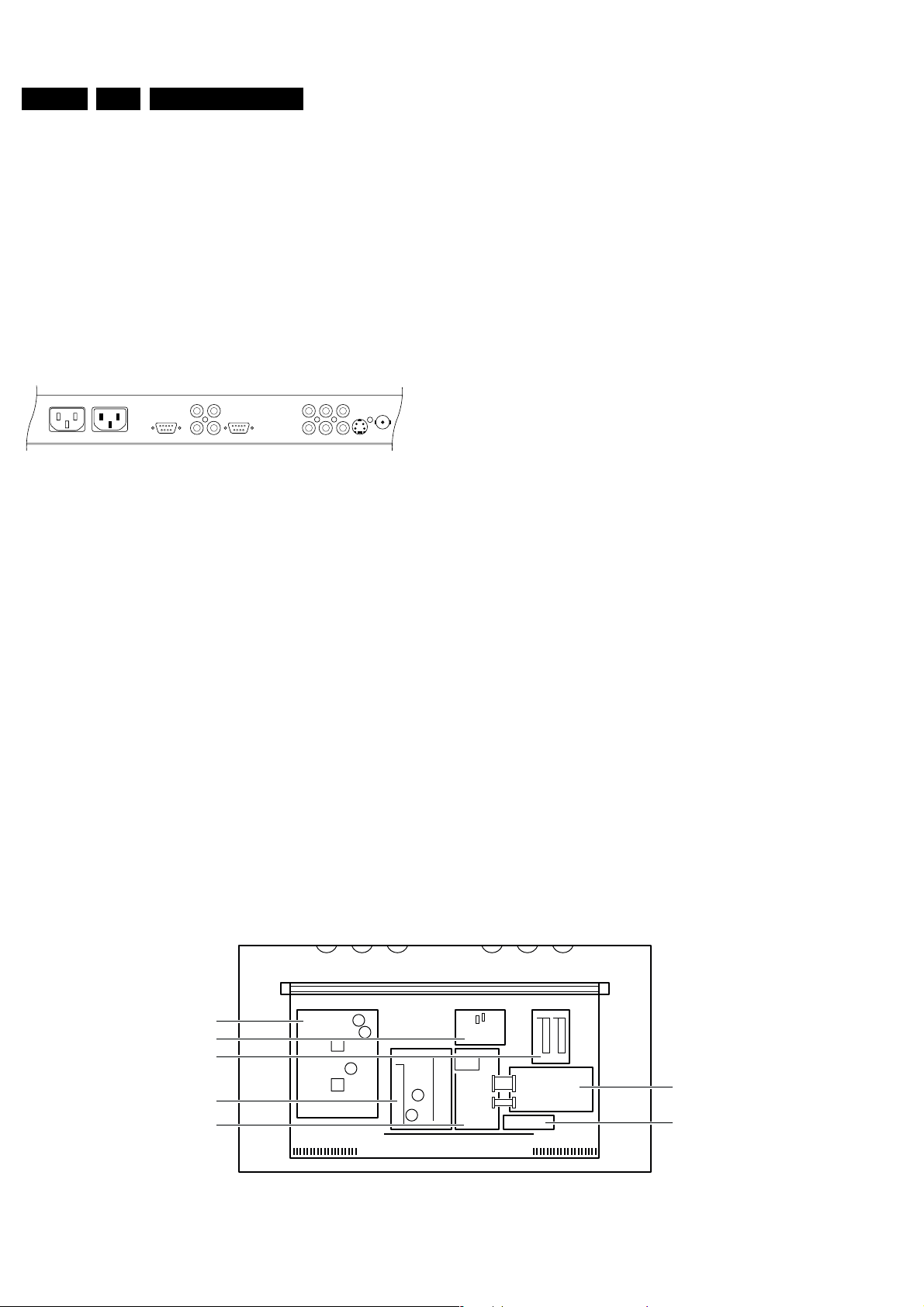
1.2 Connection facilities
1.2.1 Specification of the terminal sockets
MAINS OUTLET MAINS INLET
VGA IN VGA OUT
VGA-in
1 - R (0.7Vpp 75
2 - G (0.7Vpp 75
3 - B (0.7Vpp 75
4 - Reserved
5 - Bus-gnd
6 - R-gnd
7 - G-gnd
8 - B-gnd
9 - RC5
10- GND
11- Config_Ident
12- Bus1 (TxD/
Rxd or SDA)
13- Hsync
14- Vsync
15- Bus2 (TxD/
RxD or SDA)
VGA-out
1 - R (0.7Vpp 75
L
AUDIO IN AUDIO OUT
R
Figure 1-1
Ω)
Ω)
Ω)
Ω)
: 50Hz - 60Hz
LRYUCVBS
AUDIO IN
V
Y/C
CVBS
S-VHS
CL96532058_005
240899
2 - G (0.7Vpp 75
3 - B (0.7Vpp 75
Ω)
Ω)
4 - Reserved
5 - gnd
6 - R-gnd
7 - G-gnd
8 - B-gnd
H
H
H
H
9 - Reserved
10- GND
11- Reserved
12- Reserved
13- Hsync
14- Vsync
15- Reserved
Audio VGA-in
- Cinch Audio L(0.5Vrms >= 10k
- Cinch Audio R(0.5Vrms >= 10k
Ω)
Ω)
q
q
Audio VGA-out
- Cinch Audio L(0.5Vrms >= 1k
- Cinch Audio R(0.5Vrms >= 1k
Ω)
Ω)
q
q
SVHS
1-GND
2-GND
H
H
H
H
H
3 - Y (1Vpp / 75
4 - C (0.3Vpp / 75
Audio_in:
- Cinch Audio L (0.5Vrms >= 10kΩ)
- Cinch Audio R (0.5Vrms >= 10kΩ)
Ω )
Ω )
H
H
j
j
q
q
CVBS
- BNC - CVBS (1Vpp / 75
Ω)
YUV
- Y (1Vpp / 75
3 - U (1Vpp / 75
4 - V (1Vpp / 75
Ω )
Ω )
Ω )
q
q
q
1.3 Chassis overview
VS/VA Supply
PDP Discharge
Audio Amplifier
Pre-conditioner
AV Control
Figure 1-2
CL 96532069_131.EPS
120899
PDP Limesco
YUV/YC Input
Page 3

Safety instructions, warnings and notes
2. Safety instructions, warnings and notes
GB 3FTV1.9DE 2.
2.1 Safety instructions
It is not allowed to operate the FTV-set without glass plate. One
function of this glass plate is to absorb Infrared Radiation.
Without this glass plate the level of Infrared Radiation produced
by the plasma display could damage your eyes.
1. Safety regulations require that during a repair:
– the set should be connected to the mains via an
isolating transformer ( in this particular case a
transformer of ≥ 800 VA);
– safety components, indicated by the symbol h ,
should be replaced by components identical to the
original ones;
2. Safety regulations require that after a repair the set must
be returned in its original condition. In particular attention
should be paid to the following points.
– Note: The wire trees should be routed correctly and
fixed with the mounted cable clamps.
– The insulation of the mains lead should be checked for
external damage.
– The electrical DC resistance between the mains plug
and the secondary side should be checked (only for
sets that have a mains isolated power supply). This
check can be done as follows:
• unplug the mains cord and connect a wire between
the two pins of the mains plug;
• set the mains switch to the on position (keep the
mains cord unplugged!);
• measure the resistance value between the pins of
the mains plug and the metal shielding of the tuner
or the aerial connection on the set. The reading
should be between 4.5 MΩ and 12 MΩ;
• switch off the TV and remove the wire between the
two pins of the mains plug.
– The cabinet should be checked for defects to avoid
touching of any inner parts by the customer.
hhhh
4. If DST reacts with 'error 2', there is no communication
between set and DST. Note that IR-transmitter LED is
positioned at right side of IR-receiver eye of the E-box.
Take into account that receiver-LED on DST is positioned
not in the middle but at the left side. Point corresponding
LED's to each other. In case the amount of Infrared
produced by the screen pollutes the communication, the
set can be set in Standby-mode. Then still the errormessages can be retrieved.
2.2 Warnings
1. ESD
All ICs and many other semiconductors are susceptible to
electrostatic discharges (ESD w). Careless handling during
repair can reduce life drastically. When repairing, make sure
that you are connected with the same potential as the mass of
the set by a wristband with resistance. Keep components and
tools also at this same potential.
1. Available ESD protection equipment:
2. Never replace modules or other components while the unit
3. When making settings, use plastic rather than metal tools.
w
– complete kit ESD3 (combining all 6 prior products -
small table mat) 4822 310 10671
– wristband tester 4822 344 13999
is switched on.
This will prevent any short circuits and the danger of a
circuit becoming unstable.
2.3 Notes
1. A glass plate is positioned before the plasma display. This
glass plate can be cleaned with a slightly humid cloth. If
due to circumstances there is some dirt between the glass
plate and the plasma display panel it is recommended to do
some maintenance by a qualified service employee only.
2. Never disconnect the power display cable when the set is
operating
3. With DST no failures (error-codes) can be red, when the
set is in Service-mode.
Page 4

GB 4 FTV1.9DE3.
3. Directions for use
73mm /2.87"
406mm /16"
Directions for use
5
5
10
x 4x 4
a
4
x 2
b
4
Page 5

Directions for use
a
b
6
x 6
L
GB 5FTV1.9DE 3.
VGA OUT
AUDIO OUT
R
AUDIO IN
MAINS INLET
1 32 42
VGA IN
5
Page 6

GB 6 FTV1.9DE3.
15-pin D sub
(2-row)
15-pin mini D sub
(3-row)
a
VGA 640x480 31.468 kHz 60 Hz
Use of the remote control
Computer Display modes
VGA 640x400 31.468 kHz 70 Hz
VGA 640x350 31.468 kHz 70 Hz
MAC II 640x480 35.000 kHz 67 Hz
SVGA 800x600 35.156 kHz 56 Hz
XGA 1024x768 45.000 kHz 56 Hz
Directions for use
the monitor.
A green indicator lights up and the screen comes on.
When the monitor does not receive a certain VGA signal the screen remains
black.
When a VGA computer is connected, the selection is made automatically.
A message is displayed when the monitor does not support one of the above
mentioned VGA modes.
Switch your computer to a correct display mode.
Insert the mains plug 5 (see previous page for the illustration) supplied
into the mains inlet at the back of the monitor and in the wall socket.
Please, only use the supplied rim-earthed mains cord with its built-in filter.
&
Operation
Remote control: remove the cover of the battery compartment.
Insert the 2 batteries supplied (Type LR6AA-1.5V).
The batteries supplied do not contain the heavy metals mercury and cadmium.
Nevertheless in many countries batteries may not be disposed of with your
household waste. Please check on how to dispose of batteries according to local
regulations.“Switch the monitor on : Press the power button B at the right side of
é
Make sure that your PC is switched on and is in the correct display mode.
English
printed on the first pages of this instruction booklet.
Make sure that the wall mount is being fixed securely enough so that it meets
Unpacking and wall mounting instructions
For the unpacking instructions follow the illustrated steps printed on the
safety standards.The weight of the monitor (excl. packaging) is about 43 kg.
packaging (outside and inside).
For the wall mounting instructions follow the illustrated steps ‘ to §
Connect your computer
L
(right) and
AUDIO IN R
connector at the rear side of the
VGA IN
monitor.Fix the connectors firmly with the screws on the plug.
outputs of your Multimedia computer and to the
Connect one end of the VGA cable 1 supplied to the video card of the
computer and the other end to the
In case of a Multimedia computer,connect the audio cable 2 to the audio
(left) inputs of the monitor.
Daisy chaining
The Active Loop Through facility makes it possible to make a daisy chain with
a second VGA monitor.“Connect one end of another VGA cable 3 to the
&
é
inputs
R
and
connector of a
connector at
VGA IN
AUDIO IN L
VGA OUT
outputs of the monitor and to the
R
and
with the monitor.
of the second VGA monitor.
the rear side of the monitor and the other end to the
second VGA monitor.
Note: only use the VGA cables supplied or use cables that are specially delivered
In case of a Multimedia computer, also connect the audio cables 4 to the
AUDIO L
Connect your Apple Macintosh* computer
Attention: Macintosh computers with separate H and V synchronisation signals
can be used together with the supplied adaptor. Macintosh computers with
Composite Sync and Sync on Green signals may need a special (not
supplied) adaptor or cable. Contact your dealer.
‘
connector on the back of the
VGA IN
1234
off off on on
Connect the supplied switchable adaptor for Apple video connectors to one
end of a VGA cable.
Put the DIP switches on the adaptor in the following positions :
monitor.
Connect the end of the VGA cable with the adaptor to the video card of the
computer and the other end to the
2
1
Screw the connectors down firmly.
* Apple Macintosh is a registered trademark of Apple Computer, Inc.
Page 7

Directions for use
VGA OK
FRONT o
AV1 p MENU π
AV2 œ
AV3
¬
AV4
SMART
CONTROLS
PICTURE SOUND
- CH/P +-V+
B
Transport
Keep the original packaging to transport the
monitor if needed.
higher altitude, the picture becomes
unstable and the picture performance is
deteriorating. Bringing the set below 2000
m it works fine again.Transportation has
End of life directives
Philips is paying a lot of attention to
produce environmentally-friendly in green
focal areas.Your new monitor contains
materials which can be recycled and
reused.
At the end of its life specialised companies
no influence.
Control of peripheral equipment
The infrared signals of the screen may
influence the reception sensitivity of other
peripherals. Solution:replace the batteries
of the remote control or change position
of other equipment. E.g.keep away a
can dismantle the discarded monitor to
concentrate the reusable materials and to
minimise the amount of materials to be
disposed of.
Please ensure you dispose of your old
monitor according to local regulations.
How to dispose of batteries ?
The batteries supplied do not contain the
heavy metals mercury and cadmium.
wireless headphone from within a radius
of 1.5 m.
No stable or not synchronised VGA
picture
Check if you have selected the correct
VGA mode in your PC (640x480,
640x400, 640x350,MAC II, SVGA, XGA).
No picture or no sound
Are the supplied cables connected
Nevertheless in many countries batteries
may not be disposed of with your
household waste. Please ensure you dispose
of batteries according to local regulations.
properly? (The power cable to the display,
the VGA cables, the audio cables,...)
Is your PC switched on?
Do you see a black screen and the
indicator in front of the monitor lights up
Miscellaneous
. Ambient temperature: + 5~ + 45°C
. Maximum operating altitude: 2000 m
. Mains: AC 100-240V
green, this means that the display mode is
not supported.
Switch your VGA source to a correct
mode.
Display: 42.5 kg
. Power consumption: around 350W
. Standby consumption: 1 W
. Weight (excl. packaging)
Remote control
If your monitor no longer responds to the
remote control, the batteries may be
Display: 122.2 x 68.1 x 14.6 cm
. Dimensions (wxhxd):
. Wall mounting bracket included
exhausted.
If your problem is not solved:
Switch your monitor off and then on
again.
Never attempt to repair a defective
monitor yourself.
Check with your dealer or call a TV
GB 7FTV1.9DE 3.
technician.
Tips
Ambient temperature
Do not hang up the monitor above a
central heating or other heating sources.
Active Loop Through
The Active Loop Through facility makes it
possible to make a daisy chain for VGA.
Maximum 2 sets.
Care of the screen
Clean the anti-reflex coated flat glass
screen with a slightly damp soft cloth. Do
not use abrasives solvents as it can
damage the glass surface of the screen.
Plasma Display characteristics
When switching over to another picture
after having displayed the same still picture
for a long time (many hours), it may
happen that some parts from the previous
picture will remain on screen due to a
kind of memory effect.This ghost picture
will disappear after some time.To avoid
this effect change the pictures regularly or
for PC use you can turn on a screen saver
in your computer.
Philips has built in an automatic shift of
the picture every 5 minutes to avoid this
effect and to prolong the life of the
screen.
Very incidentally and after a longer period
of unuse (approx. 1 year) the screen may
display some strange colour deficiencies.
This is quite normal for plasma displays
and these effects will disappear after the
set has been turned on for some time.
A plasma display consists of more than 1,2
Million colour pixels. It is within industry
standards that very few pixels (< 0.001%)
may be defective, even for a new set.
There is however no reason to doubt
about the quality of the set.
The plasma display technology operates
with rare gases which are being influenced
by air pressure. Up to an altitude of 2000
m above sea-level, the display is
functioning fine. Operating the set at a
4
3
menu on/off
VGA
no function
menu.
to activate your choice
OK
no function
no function
no function
VGA
FRONT
to switch the
MENU
no function
B
Use of the remote control
Use of the remote control
mode, press the p or π keys to
VGA
cursor keys to select your choice and to
alter a selected adjustment
pπ Picture format
In
switch between a 4:3 or a 16:9 picture
format.
¬ Mute key
temporarily mute the sound or restore it
no function
- CH/P +
SMART CONTROLS
PICTURE/SOUND
VGA menu
menu.
VGA
key to switch on the
MENU
Press the
Select one of the symbols with the o and œ keys:
H for contrast
&
é
for colour temperature
for horizontal picture position
G for brightness,
VGA
key again to switch off the
MENU
for vertical picture position
Press the p and π keys to alter the selected adjustment.
Press the
V for volume
“
‘
AV1 , AV2, AV3,AV4
V press - or + to adjust the volume
Page 8

GB 8 FTV1.9DE4.
Mechanical instructions
4. Mechanical instructions
4.1 Introduction:
There are pre-defined service positions for the following
panels:
1. VS/VA SUPPLY panel.
2. PDP DISCHARGE panel.
3. AUDIO AMPLIFIER panel.
4. PRE-CONDITIONER panel.
5. AV CONTROL panel.
6. PDP LIMESCO panel.
7. YUV/YC INPUT panel.
8. LED DISPLAY panel.
9. SWITCH DISPLAY panel.
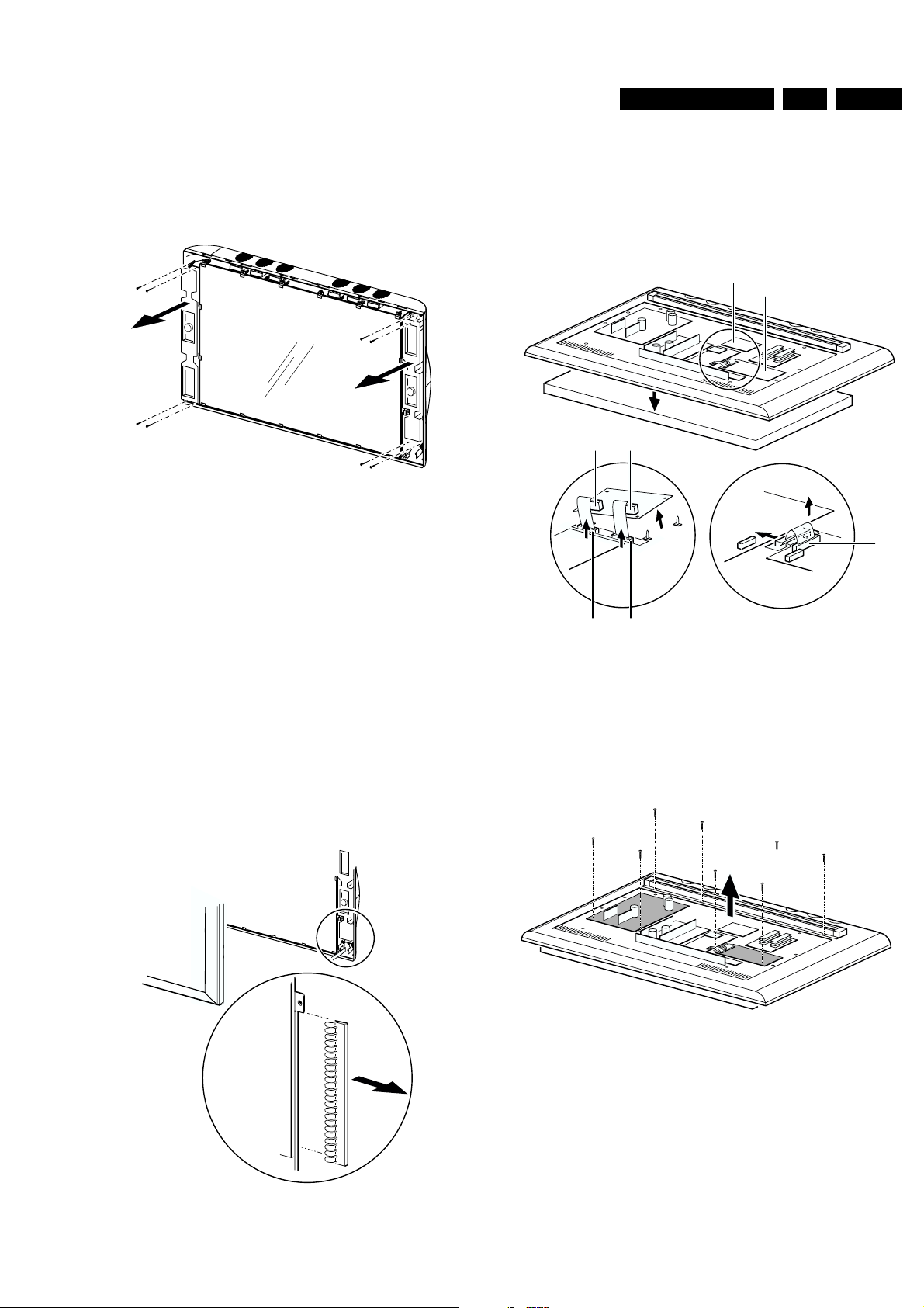
Before these panels can be accessed, the rear cover has to be
removed:
2
1
CL 96532069_130.EPS
120899
4.1.1 VS/VA SUPPLY panel.
VS/VA Supply
FD07
1
2
4
CL 96532069_132.EPS
Figure 4-3
1. Disconnect Fan Supply cable from connector FD07 in the
upper left corner [1].
2. Remove the 7 fixation screws of the panel [2].
3. Place panel on the 2 hinges, which are located near the
right corners of the panel [3].
4. Use the mechanical service part (extension cable
assembly, 12NC: 3122 785 90006) to extend the Fan
Supply cable [4].
5. The copper side is now accessible from the left.
3
120899
Figure 4-1
1. Place the Display Box in the service stand via 2 reinforced
cushions (order code: 3122 126 30181).
2. Remove the 9 fixation screws of the rear cover.
3. Remove the rear cover (during removal push it slightly
upwards).
VS/VA Supply
PDP Discharge
Audio Amplifier
Pre-conditioner
AV Control
CL 96532069_131.EPS
Figure 4-2
1. All panels are now accessible.
120899
PDP Limesco
YUV/YC Input
4.1.2 PDP DISCHARGE panel.
As in the FTV 1.5, this panel must be exchanged completely if
defective.
4.1.3 AUDIO AMPLIFIER panel.
Audio Amplifier
1
2
3
2
CL 96532069_134.EPS
120899
Figure 4-4
Page 9

Mechanical instructions
GB 9FTV1.9DE 4.
1. Some testpoints are accessible at the B-side [1].
2. If this is not sufficient, remove the 3 fixation screws of the
panel [2].
3. Panel now can be hinged on the left side to access the Aside (soldering side) [3].
4.1.4 PRECONDITIONER panel.
Pre-conditioner
3
2
2
1
5
5
1
5
CL 96532069_135.EPS
Figure 4-5
1. Disconnect the 2 grounding wires from the shielding plate
by pressing the small lever on the connector while pulling
[1].
2. Remove the 2 ferrite ring cores from their fixations [2].
3. Remove the 5 fixation screws of the panel [3].
4. Place panel on the 2 hinges, which are located, near the
left corners of the panel [4].
5. Reconnect grounding wires to the extra connectors on the
shielding plate at the left side [5].
6. The copperside becomes accessible now from the right
side.
4.1.6 PDP LIMESCO panel.
PDP Limesco
1
4
1
2
1
1
CL 96532069_137.EPS
4
120899
Figure 4-7
120899
All SMC's are located on the B-side, so all testpoints are
accessible. In case some components must be (de)soldered,
the hinge construction can be used to access the A-side.
1. Remove the 4 fixation screws of the panel [1].
2. Panel can now be hinged to access soldering side [2].
4.1.7 YUV/YC INPUT panel.
YUV/YC Input
4.1.5 AUDIO VIDEO CONTROL panel.
AV Control
CL 96532069_136.EPS
Figure 4-6
This panel has no service position for accessing the A-side,
however all service test points are accessible at the B-side (see
Service Manual).
In case some components must be (de)soldered, all fixation
screws (6 for the panel, 5 at the metal connector plate) and all
cables must be removed to access the A-side.
120899
SVHS BNC
3
2
2
1
CL 96532069_138.EPS
120899
Figure 4-8
This panel has no pre-defined service position. For access of
the A-side, the panel has to be removed:
1. Remove the 4 screws at the metal connector plate [1].
2. Remove the 2 fixation screws of the panel [2].
3. Panel can be removed now to access the A-side [3].
Page 10

GB 10 FTV1.9DE4.
Mechanical instructions
4.1.8 LED DISPLAY panel.
2
1
Figure 4-9
1. Remove 2 x 2 screws at the sides and 4 screws at the
bottom of the front cover [1].
2. Remove the front cover (it hinges at the top). During
removal unplug the cable of the LED DISPLAY panel at the
SWITCH DISPLAY panel (connector SD11) [2].
2
CL 96532069_139.EPS
120899
4.1.9 SWITCH DISPLAY panel.
1. Remove front cover (for a description see Chapter 1.1.8
'LED DISPLAY panel').
3
CL 96532069_141.EPS
Figure 4-11
1. The SWITCH DISPLAY panel can be removed now by
unscrewing 3 fixation screws [3].
4.2 Exchanging parts
120899
3
CL 96532069_140.EPS
Figure 4-10
1. The LED DISPLAY panel can be removed now by
unscrewing 1 fixation screw [3].
120899
Some parts of the FTV1.9 Display Box must be exchanged if
defective:
1. GLASS PLATE.
2. LOUDSPEAKER.
3. PLASMA DISPLAY PANEL [PDP].
4.2.1 Exchanging of the GLASS PLATE.
1. First unplug (remove Mains and VGA cable) the Display
Box .
2. Remove front cover (for a description see Chapter 1.1.8
'LED DISPLAY panel').
2
5
34
CL 96532069_142.EPS
120899
Figure 4-12
1. Now the GLASS PLATE can be removed by unscrewing all
screws [3] and removing all glass clips [4].
Page 11
Mechanical instructions
CL 96532069_145.EPS
120899
1
4
5
3
2
3
FD173 FD171
PDP Discharge
PDP Limesco
PD3
CN24
CN23
FOAM CUSHION
GB 11FTV1.9DE 4.
4.2.2 Exchanging of a LOUDSPEAKER.
1. First unplug (remove Mains and VGA cable) the Display
Box.
2. Remove front cover (for a description see Chapter 1.1.8
'LED DISPLAY panel').
3
4
3
CL 96532069_143.EPS
Figure 4-13
1. The LOUDSPEAKER can now be removed by
disconnecting its cable and removing the 4 fixation screws
at the top and bottom of the speakerbox. Be sure to remove
the correct screws, otherwise the speaker system will be
damaged (it is an airtight system).
1. Remove all copper EMC SHIELDING springs mounted
around the display [6].
2. Now flip the complete Display Box and place it with the
Plasma Display down on a foam cushion. Be 100 % sure
a large foam cushion is placed underneath the PDP, as it
will drop about 10 mm after removing its fixation screws ! !
3. Disassemble metal rear cover (for a description see
Chapter 1.1 'Introduction').
3
4
3
120899
4.2.3 Exchanging of the PDP.
1. First unplug (remove Mains and VGA cable) the Display
Box.
2. Place the rear side of the Display Box on a foam cushion
(be sure the metal rear cover is mounted in order to prevent
damaging of the electronic panels).
3. Remove front cover (for a description see Chapter 1.1.8
LED DISPLAY panel).
4. Now the GLASS PLATE can be removed by unscrewing all
screws and removing all glass clips (for a description see
Chapter 1.2.1. 'Exchanging of the GLASS PLATE').
6
Figure 4-14
CL 96532069_144.EPS
120899
Figure 4-15
1. Disconnect the following cables:
– Cables coming from connectors CN23 and CN24 of the
PDP DISPLAY panel [3] (for easiest access lift the
PDP DISCHARGE panel from its fixations [2]).
– Flat cable on connector PD3 of the PDP LIMESCO
panel [4]. Also remove the ferrite 'flat cable shield'
completely by unlocking its fixations [5].
1
2
2
1
1
3
2
2
1
CL 96532069_146.EPS
Figure 4-16
1. Now remove the 8 large screws which hold the PDP:
– 4 screws are located at the top: they also hold the
aluminium wall mount [1].
– The other 4 are located at the bottom: the 2 outer
screws are hidden behind panels. Therefor unscrew
the VS/VA SUPPLY and the PDP-LIMESCO panel
(grey panels) [2].
2. Lift encasing from PDP and replace PDP [3].
120899
Page 12

GB 12 FTV1.9DE5.
Service modes, fault finding and repair tips
5. Service modes, fault finding and repair tips
For the FTV1.9, the Monitor can be used in two applications.
• A stand-alone configuration, a separate device which can
also be sold and serviced separately.
• TV configuration, where the monitor is combined with the
E-box.
The monitor, as a stand-alone unit, can be serviced by using a
test pattern coming from the PDP-LIMESCO panel on the rear
of the monitor itself or via a PC/laptop by using ComPair via the
ComPair connector.
In this chapter the following paragraphs are included:
1. Test points
2. Dealer Service Tool (DST)
3. Service Modes
4. Error code buffer and error codes
5. The "blinking LED" procedure
6. Fault-finding tips
7. ComPair
5.1 Test points
The FTV1.9 chassis is equipped with test points in the service
printing. These test points are referring to the functional blocks:
• A1-A2-A3, etc.: Test points for the Audio amplifier (A)
• C1-C2-C3, etc.: Test points for the AV control circuit
(AVC)
• FD1-FD2-FD3, etc.: Test points for the VsVa supply (FD1FD2) and the PDP discharge panel
• L1-L2-L3, etc.: Test points for the PDP LIMESCO
(PD1-PD9)
• PR1-PR2-PR3, etc.: Test points for the Pre-conditioner
(PR1-PR3)
• Y1-Y2-Y3, etc: Test points for the Y/C YUV monitor
panel (UY1-YC4)
Measurements are performed under the following conditions:
Video: colour bar signal; Audio: 3 kHz left, 1 kHz right
5.2 Dealer Service Tool (DST)
For easy installation and diagnosis the dealer service tool
(DST) RC7150 can be used. When there is no picture (to
access the error code buffer via the OSD), DST can enable the
functionality of displaying the contents of the entire error code
buffer via the blinking LED procedure, see also paragraph 5.5.
The ordering number of the DST (RC7150) is 4822 218 21232.
5.2.1 Installation features for the dealer
The dealer can use the RC7150 for programming the TV-set
with pre-sets. 10 Different program tables can be programmed
into the DST via a GFL TV-set (downloading from the GFL to
the DST; see GFL service manuals) or by the DST-I (DST
interface; ordering code 4822 218 21277). For explanation of
the installation features of the DST, the directions for use of the
DST are recommended (For the FTV1.9 chassis, download
code 4 should be used).
Display Box (TV Configuration), please check chapter 5 in the
Training Manual of the Receiver Box.
5.3.1 Service Default Mode (SDM)
The purpose of the SDM is:
• Provide a situation with predefined settings to get the same
measurements as in this manual.
• Access to the error buffer via the blinking LED procedure.
• Inspection of the error buffer.
• Possibility to overrule software protections via the service
pins (caution: override of software protections! ).
Entering the SDM:
• By transmitting the "DEFAULT" command with the RC7150
Dealer Service Tool (this works both while the set is in
normal operation mode or in the SAM).
• By pressing on a standard RC the following sequence 0, 6,
2, 5, 9, 6 followed by the "MENU" key.
• By short-circuiting the SDM pin on the µP panel.
In the SDM the following information is displayed on the
screen:
--------------------------------------------------------------
F19DBC X.Y_12345 (1) LLLL (2) SDM (3)
ERR 02 01 14 ## ## ## ## ## ## ##
--------------------------------------------------------------
Explanation notes/references:
(1) Software identification of the main micro controller
(F19DBC X.Y_12345)
• F19D is the chassis name for FTV1.9 display
• B is the region identification
• C is the language cluster
• X = (main version number)
• Y = (subversion number)
• ##### are 5 digits of the serial number
(2) "LLLL" Normal display operation in hours
(3) "SDM" To indicate that the TV set is in the service default
mode
(4) "ERR 02 01 14 ## ## ## ## ## ## ## ##" This line shows
the contents of the error buffer (max. 10 errors). The last error
that occurred is displayed at the most left position. When less
then 10 errors have occurred the rest of the line is empty. When
the errorlist is empty " No errors" is displayed. No duplicate
errors.
Exit the SDM:
Push the "STANDBY" button on the Remote Control.
The SDM sets the following pre-defined conditions:
• Volume level is set to 25% (of the maximum volume level).
• Linear Audio and Video settings are set to 50%.
• Colour temperature is set to normal.
The following functions are "overruled" in SDM since they
interfere with diagnosing/repairing a set
• Video blanking.
• Slow demute.
• Anti-ageing.
• Automatic switch to "Standby" when H- and/or V-sync
signals are lost.
All other controls operate normally.
5.2.2 Diagnose features for service
FTV1.9 sets can be put in two service modes via the RC7150.
These are the Service Default Mode (SDM) and the Service
Alignment Mode (SAM).
5.3 Service Modes
Below described sequence is only valid for the "Monitor Only
Configuration". When a Receiver box is connected to the
5.3.2 Service Alignment Mode (SAM)
The purpose of the SAM is to align and or adjust settings.
For recognition of the SAM, "SAM" is displayed at the top of the
right side of the screen
Entering the SAM-menu:
• By pressing the "ALIGN" button on the RC7150 Dealer
Service
• Standard RC sequence 062596 followed by the "OSD"
button.
Page 13

Service modes, fault finding and repair tips
GB 13FTV1.9DE 5.
• By short-circuiting the SAM pin on the µP panel (Caution:
override of software protections ! ! )
In the SAM the following information is displayed on the screen:
--------------------------------------------------
F19DBC X.Y_12345 SAM
ERROR## ## ## ## ##
WHITE POINT
PDP TEST PATTERN [ON/OFF]
STORE
RESET ERROR BUFFER
--------------------------------------------------
The menus and submenus
White point
The white point sub menu contains the following items:
•RED
• GREEN
•BLUE
• COLOUR TEMPERATURE
PDP Test pattern
By selecting this item, all OSD disappears from the screen. The
screen now changes from light grey to dark grey in a slow
regular rhythm. One can so easily check if all pixels of the
monitor are correct.
Store
The change values are stored in the NVM.
Reset Error Buffer
This option will reset the error buffer.
Exit the SAM:
Push the "STANDBY" button on the Remote Control.
SAM menu control:
Menu items can be selected with the "UP" or "DOWN" key.
Entry into the selected items (sub menus) is done by the
"LEFT" or "RIGHT" key. The selected item will be highlighted.
With the same "LEFT/RIGHT" keys, it is possible to increase/
decrease the value of the selected item.
Return to the former screen by pushing the "MENU" button.
The item values are stored in NVM if the sub menu is left.
5.3.3 Customer Service Mode (CSM) Display
FTV1.9 monitors are equipped with the "Customer Service
Mode" (CSM). CSM is a special service mode that can be
activated and de-activated by the customer, upon request of
the service technician/dealer during a telephone conversation
in order to identify the status of the set. This CSM is a 'read
only' mode, therefore modifications in this mode are not
possible.
Entering the Customer Service Mode.
• By pressing on RC03333/01 the following sequence :
Picture, sound, cursor up, cursor down, cursor left, cursor
right followed by the “MUTE” button.
Exit the Customer Service Mode.
• pressing the "MENU" or any key on the Remote Control
handset (except "P+" or "P-")
• switching off the TV set with the mains switch.
All settings that were changed at activation of CSM are set
back to the initial values
The Customer Service Mode information screen
The following information is displayed on screen:
--------------------------------------------------
CUSTOMER SERVICE MENU
• Software version F19DBC X.Y_#####)
• Code 1: contains the last 5 error codes
• Code 2: contains the first 5 error codes with the last
received error at the most left-hand side.
• Service unfriendly modes
--------------------------------------------------
5.4 Error code buffer and error-codes
The error code buffer contains all errors detected since the last
time the buffer was erased. The buffer is written from left to
right.
In case of non-intermittent faults, clear the error buffer before
starting the repair to prevent that "old" error codes are present.
If possible check the entire content of the error buffers. In some
situations an error code is only the RESULT of another error
code (and not the actual cause).
Note: a fault in the protection detection circuitry can also lead
to a protection
The error code buffer will be cleared in the following cases:
• exiting SDM or SAM with the "Standby" command on the
remote control
• transmitting the commands "DIAGNOSE-9-9-OK" with the
DST.
Leaving SDM or SAM with the mains switch does not reset the
error buffer.
Examples:
ERROR: 0 0 0 0 0 : No errors detected
ERROR: 6 0 0 0 0 : Error code 6 is the last and only detected
error
ERROR: 5 6 0 0 0 : Error code 6 was first detected and error
code 5 is the last detected (newest) error
Error
-nr
1 +5V +5V pin at µP is low.
2 8V6 8V6 pin at µP is low.
3 Fan_prot Gives an indication that 1 or more
4Over-
5 DC_prot Audio-amplifier IC, its supply or the
6 Over_volta
7 Vrr Powersupply of the display is not
8 Power_OKEPower supply or modules that uses
9 Blocked
10 Blocked
11 TDA9860 No acknowledge of Audio controller
12 TDA4885 No acknowledge of Video controller
13 MC141585No acknowledge of OSD Generator
14 uPD93687
Type of
Error Possible defect/cause
FAN(s) does not function, or that 1
or more fan control circuits is defect
temp_prot
ge_prot
NVM IIC
bus
slow IIC
bus
GD-LBD
Temperature at the heatsink of the
VsVa supply or the Preconditioner
is too high
Audio amplifier is defect
Vs or Va supply voltage is too high
correct. Ignorance of the signal
during startup by the software.
this voltage. If this signal is NOT
activated means that all supply
voltages are available (exception
Audio supply )
NVM IIC bus is not correct
Slow IIC bus is not correct
No acknowledge of Limesco
Page 14

GB 14 FTV1.9DE5.
Service modes, fault finding and repair tips
Error
-nr
15 PCF8574ATNo acknowledge of I/O Expander
16 NVM No acknowledge of NVM
17 Communic
Type of
Error Possible defect/cause
Fault in the communication
ation
5.5 The "blinking LED" procedure
The contents of the error buffer can also be made visible
through the "blinking LED" procedure. This is especially useful
when there is no picture. There are two methods:
• When the SDM is entered, the LED will blink the contents
of the error-buffer. Error-codes = 10 are shown as followed.
A long blink of 1second which is an indication of the
decimal digit, followed by a pause, followed by n short
blinks. When all the error-codes are displayed, the
sequence is finished with a led display of about 3 seconds.
The sequence starts again.
• With the DST all error codes in the error buffer can be
made visible. Transmit the command: "DIAGNOSE x OK"
where x is the position in the error buffer to be made visible
x ranges from 1, (the last (actual) error) to 10 (the first
error). The LED will operate in the same way as in the
previous point, but now for the error code on position x.
Example:
Error code position 1 2 3 4 5
Error buffer: 12 9 5 0 0
• after entering SDM: 1 long blink of 1 sec. + 2 short blinks
- pause - 9 short blinks - pause - 5 short blinks - pause long blink of 3 sec. --etc.
• after transmitting "DIAGNOSE- 1- OK" with the DST: 1 long
blink 2 short blinks - pause - 1 long blink + 2 short blinks
- etc.
• after transmitting "DIAGNOSE- 2- OK" with the DST: blink
(9x) - pause - blink (9x) - etc.
• after transmitting "DIAGNOSE- 3- OK" with the DST: blink
(5x) - pause - blink (5x) - etc.
• after transmitting "DIAGNOSE- 4- OK" with the DST:
nothing happens
5.6 Protection structure
5.6.1 General
The protection structure of the FTV1.9 D-box is shown at figure
5.5.
The FTV1.9 monitor has one microprocessor, which is situated
on the AV-control panel and is supplied by the 5V standby
supply. The microprocessor is even active when the set is
switched to standby. The microprocessor controls the "supplyon" line which switches first relay 5680 and then relay 5690.
In de standby-mode or the protection-mode the "supply-on" line
is "low" and both relays are switched off. The preconditioner is
disconnected from the mains.
The protections of the FTV1.9 monitor can be divided into 5
subgroups:
– Fan_prot
– Over_temp_prot
– DC_prot
– Over_voltage_prot
–Vrr
For the Fan-, Over_temp, DC and the Over_voltage protections
the signals for the µP are latching, using the 5Vstby_switched
for powering the circuits permanently. The µP has sufficient
time for diagnosis and for storing the error-codes in the NVM.
Vrr, which is an indication of the powersupply of the display is
correct, is directly fed to the µP.
5.6.2 Signal line "PROTECTION STATUS" and errorcodes
When one of the protection mechanism is triggered, the
5Vstby-switched is connected via a saturated transistor and a
pre-defined resistor to signal line "protection status", which is
connected to the µP.
Signal line "protection status" is connected to ground via
resistor R3378 and 3379. For each separate fault condition
mechanism we get a pre-defined voltage at the µΠ.
This results in the following table
Protectionmode
None ----- < 0.3V none
Fan_prot 1K
Vs or
Va_prot
Temp_prot 220
DC-prot 68
Vrr ------ ------ 7
Protection signal Vrr coming from the PDP, to indicate that the
powersupply is ok or not ok ( "1" or "0" ) is directly connected
to the µP. Error-code 7 is stored in the NVM and the set is
switched to standby.
When one of the protections is activated, the power supplies of
the Vs and Va are shut down and the set is switched to
standby.
5.6.3 Fan protection
When this protection is activated, the Va- and Vs power supply
are shut down. The set is switched to the standby mode and
error-code 3 is stored in the NVM.
The fan voltage is powered by 17V, but clamped to 12V to
prevent damage. In order to be able to verify whether the fans
are running, a fault detection circuit is implemented for each of
the 6 fans. A running fan gives pulses in the same speed as the
rotation of the blades. The circuit uses these pulses to trigger
the discharge of an elcap. The elcap is continuously charged
through a resistor.
Example : Capacitor C2319 is charged through R3356 and at
every pulse discharged by T7322. When fan 6 is blocked,
C2314 is charged via D6326 en triggers thyristor 7315,
because C2319 is no longer discharged via T7322. The current
now flows from the 5Vstby-switched via resistor 3383 and 3325
driving transistor T7321 into saturation. The voltage dividing of
R3323 and resistor R3378 and 3379 now determine the
voltage "protection status". (neglect the Vce of 0.2V of T7321.).
Reset of the VsVa-supply.
Transistor T7339 is shorted now by the presence of the
"protection status" signal. T7339 connects resistor R3376 and
R3389 to ground, switching on T7338. Thyristor 7333 is now
triggered, shorting signal PROTS to ground. To follow the
signal flow, go to the right upper corner of schematic FD1.
Connecting PROTS to ground, will start a current flow through
opto-coupler diode 7103 and the opto-coupler transistor
connects supply voltage Vcc2 to the fault input ( pin 10 ) of IC
7101. When the voltage at pin 10 exceeds 1.0V, IC7101 stops
oscillating. The Va-supply stops functioning.
To continue the signal flow, go to the right upper corner of
schematic FD2. Connecting PROTS to ground also results in a
current flow through the opto-coupler diode of 7003. The optocoupler transistor connects supply voltage Vcc1 to the fault
input ( pin 10 ) of IC 7001. When the voltage at pin 10 exceeds
1.0V, IC7001 stops oscillating. The Vs-supply stops
functioning.
Series
resistor
Ω
Ω
470
Ω
Ω
Voltage at "protectionstatus" line
0.30V < Vprot < 1.90V 3
1.90V < Vprot < 2.80V 4
2.80V < Vprot < 3.75V 5
3.75V < Vprot < 4.7V 6
Errorcode
Page 15

Service modes, fault finding and repair tips
GB 15FTV1.9DE 5.
5.6.4 Vs and Va protection
Va protection
When this protection is activated, the Va- and Vs power supply
are shut down. The set is switched to the standby mode and
error-code 4 is stored in the NVM.
When the Va-supply exceeds the 68V, regulator 7112 is
triggered and will switch on T7113. Capacitor 2132 is charged
via the 5Vstby-switched and will trigger thyristor 7114, which
will switch on T7341. The voltage dividing of R3386 and
resistor R3378 and 3379 now determine the voltage "protection
status". ( neglect the Vce of 0.2V of T7341 ). See schematic
FD2.
The presence of the voltage at "protection status" line will
eventually reset the VsVa-supply. For more info see
subparagraph - Reset of the VsVa-supply.
Vs protection
When this protection is activated, the Vs power supply is shut
down. The set is switched to the standby mode and error-code
4 is stored in the NVM.
When the Vs supply exceeds the 198V, regulator 7012 is
triggered and will switch on T7016. Capacitor 2032 is charged
via the 5Vstby-switched and will trigger thyristor 7013. Thyristor
7013 is fired and connects signal Aa to ground. To follow the
signal flow, go to the right upper corner of schematic FD1.
When signal Aa is shorted to ground, T7341 is switched on.
The voltage dividing of R3386 and resistor R3378 and 3379
now determine the voltage "protection status". ( neglect the
Vce of 0.2V of T7341 ). See schematic FD2.
The presence of the voltage at "protection status" line will
eventually reset the VsVa-supply. For more info see
subparagraph - Reset of the VsVa-supply.
5.6.5 Temperature Protection
When this protection is activated, the Va- and Vs power supply
are shut down. The set is switched to the standby mode and
error-code 5 is stored in the NVM.
When the temperature of the heatsink on the Preconditioner
panel or on one of the 2 heatsink on the VsVa panel exceeds
the 110°C, the PTC resistance increases drastically. The
voltage at pin 3 of IC7330 will drop and the output of 7330 will
do the same. The current flow through opto-coupler diode 7331
results also in a current flow through the opto-coupler transistor
and will trigger thyristor 7332. The fired thyristor switches
transistor 7337 on. The voltage dividing of R3339 and resistor
R3378 and 3379 now determine the voltage "protection status".
( neglect the Vce of 0.2V of T7337 ).
The presence of the voltage at "protection status" line will
eventually reset the VsVa-supply. For more info see
subparagraph - Reset of the VsVa-supply.
5.6.6 DC Protection - Audio Amplifier
When this protection is activated, the Va- and Vs power supply
are shut down. The set is switched to the standby mode and
error-code 6 is stored in the NVM.
In case of a fault in the Audio amplifier or when a DC voltage
appears on the speaker output, a signal called DCPROT is
generated. See schematic FD2 - F7. In case of a fault,
thyristor 7314 is triggered and switches on T7340. The voltage
dividing of R3380 and resistor R3378 and 3379 now determine
the voltage "protection status". ( neglect the Vce of 0.2V of
T7340 ).
The presence of the voltage at "protection status" line will
eventually reset the VsVa-supply. For more info see
subparagraph - Reset of the VsVa-supply.
5.6.7 Vrr - PDP supplies
Vrr is a logical signal ( "high" in normal circumstances ) that
comes from the PDP. It's purpose is to trigger the switch-off of
the Pre-conditioner supply in case Vrr becomes "low" , to
trigger the shutdown of the VsVa supply and to initialise that
error-code 7 is stored in the NVM.
When signal Vrr becomes "low", see FD1 - section F13, the
output of IC7301-B becomes "high". This results in two actions.
It will trigger thyristor 7302 and short signal PROTS to ground.
This results eventually in a reset of the VsVa supply.
Switching on T7371, which again switches on T7370 via the
5Vstby-switched supply. Signal-line "supply-on" is now
grounded. This results in switching off relay 5680 and 5690,
disconnecting the mains from the pre-conditioner. The standby
supply ( 5Vstby-switched ) is still functional. (See Fig. 5-5)
5.7 Fault finding tips
5.7.1 Pre-conditioner
The Pre-conditioner delivers the following output voltages:
• 5 VSTBY
• 5 VSTBY_switched
• 380 VDC
• Internal 12 VSTBY to supply the relay, which switches the
mains input
To trouble shoot the pre-conditioner, first check the LED of the
display-box.
• No red, green or orange LED indicates the absence of the
+5Vstby_switched at the VsVa panel.
Check the +5Vstby_switched on pin 5 of connector PR08. If
this voltage is present check the presence of this voltage at the
VsVa-panel on pin 2 of connector FD04. See the wiring
diagram of the monitor for more details.
If the voltage is not present, check R3508 and fuse 1500. In
case of a defective R3508, check/replace item 7500, optocoupler 7501, regulator 7502, and diode 6501 + 6502.
In case of an open circuit of fuse 1500, check/replace bridge
6500 and capacitor C2501.
If both component are alive, measure the voltage at pin 5 of
IC7500 - Topswitch. If the waveforms resemble a burst-signal,
the output is too heavy loaded. Check the output diode D6504
and capacitor C2508 of the 12VSB and diode 6505 and
capacitor C2510 of the 5VSTBY.
• The red LED is blinking (+5Vstby is OK!), which is an
indication of a protection.
Disconnect the VGA-cable between the E-box and the Monitor.
Now the Monitor is operating as a stand-alone unit.
Switch the monitor via the DST, (command "Default") or via the
RC (special sequence) to the SDM.
Automatically the orange coloured LED of the monitor will blink
the content of the error-buffer. If the sequence contains errorcode 8, the cause could be a defective pre-conditioner. Errorcode 8 is an indication that the +5V and/or the Vs/Va of the
VsVa supply are not correct.
In case of error-code 4, switch OFF the set and check the
temperature of the heatsink. In case of a high temperature of
the heatsink, check MOSFET T7610 and the drive-circuit
around T7640, T7641 and T7608.
In case of error-code 8, remove connector PR09 from the
board. Short-circuit pin 2 of T7681 to ground, simulation of
"SUPPLY_ON". (Caution - Protections overruled!!!)
Measure voltage at C2616. Is voltage 380Vdc?
Yes, the cause was a too heavy load/short-circuit at the VsVapanel.
No, measure the voltage at C2606/C2607. Is this voltage a DCvoltage of approx. 300V with a strong ripple at a mains-input of
230Vac? If NO, check if relay 5690 is activated via the
transistors T7684 + T7690. Check also PTC's 3600, 3601 and
3602 at their resistor-value.
Page 16

GB 16 FTV1.9DE5.
Service modes, fault finding and repair tips
Voltage is present at C2606. Check/replace NFR 3663 and
3668, if one of them is an open-circuit. In case R3663 is an
open circuit, check/replace diode 6660, 6661 and capacitor
C2664 plus IC 7660. If IC7660 is defect, check/replace IC 7650
and C2262. In case of an open circuit of NFR 3668, replace IC
7650.
NFR 3663 and NFR 3668 are not defect. Measure waveform at
base of T7608. Is a square waveform present at gate of T7610?
Check/replace MOSFET T7610 and the drive-circuit around
T7640, T7641 and T7608.
5.7.2 VsVa-supply
The red LED is blinking (+5Vstby is OK!), which is an indication
of a protection.
Disconnect the VGA-cable between the E-box and the Monitor.
The Monitor is now operating as a stand-alone unit.
Switch the monitor via the DST, (command "Default") or via the
RC (special sequence) to the SDM.
• Error-code 1, check the +5V supply
Check fuse 1103. If the fuse is an open circuit, check/replace
IC 7201. If fuse 1103 is OK, check the presence of the 17V. I
this voltage is not present check fuse 1102 + 1104 and D6121
+ D6122. If the 17V is present, then remove connector FD05.
The reason could be a too heavy load or a short-circuit of the
+5V supply. If after disconnection of connector FD05 the set
still goes into protection, check D6203, NFR 3205 and the
circuit around IC 7201.
• Error-code 2, check the 8V6 supply
Check regulator IC 7203, NFR 3099 and D6204.
• Error-code 8 there is something wrong with the
POWER_OKE signal. When the POWER_OKE signal is
low, the Vs and Va and the +5V are available.
Measure the voltage Va at C2120. Is the voltage between 55V
and 65V? If not check fuse 1105 and D6120. If both
components are OK, the cause could be a too heavy load.
Measure the voltage Vs at C2020. Is the voltage between 165V
and 185V? If not check D6020. If D6020 is OK, the cause could
be a too heavy load.
If both voltage are not present, check fuse 1004 at the input.
If fuse 1004 is an open circuit, check the MOSFET's 7005 and
7006 for a short-circuit. In case of short-circuit use the repairkit.
If fuse 1004 is OK, check the voltage at pin 15 of IC 7001. Is the
voltage at pin 15 approx. 16-17V? If NO, check NFR 3002 and
D6002 + D6030. If YES, check the waveforms FD49 and FD50
at pin 14 and 12. If they are present, check pulse transformer
5001 and the driver-circuits around MOSFET 7005 and 7006.
If the waveforms FD49 and FD50 are not present, replace
IC7001.
• Error-code 5, check the audio-supply or the Audio amplifier
IC.
Check/replace fuse 1201 + 1202 and diode 6201 + 6202. If the
components are OK, check the audio-amplifier IC.
• Error-code 6, check the Vs and/or the Va supply voltage.
The regulation-circuit of one of these voltages is not working
correctly.
For the Va supply check opto-coupler 7102 and IC 7110.
For the Vs supply check opto-coupler 7002 and IC 7010
5.8 ComPair
5.8.1 ComPair mode
The figure below shows how to do it.
ComPair
TOPVIEW B-SIDE
AVC39
5
6
7
8
DEFAULT MODE
4
3
2
1
Figure 5-1
After switching ON the set, the red LED will blink as an
indication that the monitor is in the ComPair mode.
5.8.2 Introduction
ComPair (Computer Aided Repair) is a service tool for Philips
Consumer Electronics products. ComPair is a further
development on the DST service remote control allowing faster
and more accurate diagnostics. ComPair has three big
advantages:
• ComPair helps you to quickly get an understanding how to
repair the FTV1.9 in short time by guiding you step by step
through the repair procedures.
• ComPair allows very detailed diagnostics (on I2C level)
and is therefore capable of accurately indicating problem
areas. You do not have to know anything about I2C
commands yourself; ComPair takes care of this.
• ComPair speeds up the repair time since it can
automatically communicate with the FTV1.9 (when the
microprocessor is working) and all repair information is
directly available. When ComPair is installed together with
the SearchMan FTV1.9 electronic manual, schematics and
PCBs are only a mouse-click away.
ComPair consists of a Windows based faultfinding program
and an interface box between PC and the (defective) product.
The ComPair interface box is connected to the PC via a serial
or RS232 cable. In case of the FTV1.9 chassis, the ComPair
interface box and the FTV1.9 communicate via an I2C cable
(bi-directional) The ComPair fault finding program is able to
determine the problem of the defective television. ComPair can
gather diagnostic information in 2 ways:
1. Communication to the television (automatic)
2. Asking questions to you (manually)
ComPair combines this information with the repair information
in its database to find out how to repair the FTV1.9.
Automatic information gathering
Reading out the error buffer, ComPair can automatically read
out the contents of the entire error buffer.
Diagnosis on I2C level. ComPair can access the I2C bus of the
television. ComPair can send and receive I2C commands to
the micro controller of the television. In this way it is possible for
ComPair to communicate (read and write) to devices on the
I2C busses of the FTV1.9.
AVC39
5
6
7
8
ComPair MODE
CL 96532069_149.eps
4
3
2
1
190899
The monitor, as a stand-alone unit, can be diagnosed via a PC/
laptop by using ComPair via the ComPair connector. Before
connecting the ComPair-cable at the AV Control panel on
connector AVC34, the monitor must be put in the "ComPair Mode ". This can be done by changing the jumpers at
connector AVC39. Connector AVC39 is situated under the uP
panel.
Manual information gathering
Automatic diagnosis is only possible if the micro controller of
the television is working correctly and only to a certain extend.
When this is not the case, ComPair will guide you through the
faultfinding tree by asking you questions and showing you
examples. You can answer by clicking on a link (e.g. text or an
Page 17

Service modes, fault finding and repair tips
86532027_003.EPS
050898
PC VCR I2CPower
9V DC
GB 17FTV1.9DE 5.
waveform pictures) that will bring you to the next step in the
faultfinding process.
A question could be: Do you see snow? (Click on the correct
answer)
YES / NO
An example can be: Measure testpoint I7 and click on the
correct oscillogram you see on the oscilloscope
I7 B7502
1V / div DC
10µs / div
Figure 5-2
By a combination of automatic diagnostics and an interactive
question/answer procedure, ComPair will enable you to find
most problems in a fast and effective way.
Additional features
Beside fault finding, ComPair provides some additional
features like:
• Uploading/downloading of pre-sets
• Managing of pre-set lists
• Emulation of the Dealer Service Tool
9. Plug the mains adapter in the mains outlet and switch ON
the interface. The green and red LED's light up together.
The red LED extinguishes after approx. 1 second (the
green LED remains lit).
10. Start-up Compair and select "File" menu, "Open...:; select
"FTV1.9 Fault finding" and click "OK"
11. Click on the icon (Fig. 5-3) to switch ON the communication
mode (the red LED on the Compair interface wil light up)
12. Switch on the television set with the mains switch
13. When the set is in standby. Click on "Start-up in ComPair
mode from standby" in the ComPair FTV1.9 fault finding
tree, otherwise continue.
Figure 5-3
5.8.3 Searchman (Electronic Service Manual)
If both ComPair and SearchMan are installed, all the
schematics and PCB's of the faulty set are available when
clicking on the hyper-link of a schematic or a PCB in ComPair.
Example : Measure the DC-voltage on capacitor C2568
(Schematic/Panel) at the Monocarrier.
Clicking on the PCB hyper-link, automatically shows the PCB
with a highlighted capacitor C2568. clicking on the schematic
hyper-link, automatically shows the position of a highlighted
capacitor C2568 at the schematic.
5.8.4 Connecting the ComPair interface
The ComPair Browser software should be installed and setup
before connecting ComPair to the FTV1.9. (See the ComPair
Browser Quick Reference Card for installation instructions):
1. Connect the RS232 interface cable to a free serial (COMM)
port on the PC and the ComPair interface PC connector
(connector marked with "PC").
2. Place the ComPair interface box straight in front of the
television with the infrared window (marked "IR") directed
to the television LED. The distance between ComPair
interface and television should be between 0.3 and 0.6
meter. (Note: make sure that (also) in the service position,
the ComPair interface infra red window is pointed to the
standby LED of the television set (no objects should block
the infra red beam)
3. Connect the mains adapter to the connector marked
"POWER 9V DC" on the ComPair interface
4. Switch the ComPair interface OFF
5. Switch the television set OFF with the mains switch
6. Remove the rear cover of the television set
7. Connect the interface cable (4822 727 21641) to the
connector on the rear side of the ComPair interface that is
marked "I2C" (See Figure 5-4)
8. Connect the other end of the interface cable to the
ComPair connector AVC34 (0334) at the right/bottom side
of the AV-Control panel.
Figure 5-4
The set has now started up in ComPair mode. Follow the
instruction in the FTV1.9 fault finding tree to diagnose the set.
Note that the OSD works but that the actual user control is
disabled
5.8.5 Preset installation
Presets can be installed in 2 ways with the FTV1.9.
• Via infra red
– only sending TO the television
– the rearcover does NOT have to be removed
Click on "File" "Open" and select "TV - use ComPair as DST"
to use infra red
• Via cable
– sending TO the television and reading FROM the
television
– the rearcover has to be removed
Click on "File" "Open" and select "FTV1.9 fault finding" to use
the cable
Presets can be installed via menu "Tools", "Installation",
"Presets".
5.8.6 Ordering ComPair
ComPair order codes:
• Starterkit ComPair + SearchMan software + ComPair
interface (excluding transformer): 4822 727 21629
• ComPair interface (excluding transformer): 4822 727
21631
• ComPair transformer (continental) Europe: 4822 727
21632
• ComPair transformer United Kingdom: 4822 727 21633
• Starterkit ComPair software: 4822 727 21634
Page 18
GB 18 FTV1.9DE5.
Service modes, fault finding and repair tips
• Starterkit SearchMan software: 4822 727 21635
• Starterkit ComPair + SearchMan software: 4822 727
21636
• ComPair CD (update): 4822 727 21637
2032
5VSTBY-SWITCHED
VS
3036
3035
3033
3384
7016
3058
7341
7012
3385
3037
2037
3034
7114
FD1
3394
[C-14]
AA
21352132
7013
2038
3038
PROT-FAN 1-6
5VSTBY-SWITCHED
17V
7321
7340
• SearchMan CD (update): 4822 727 21638
• ComPair interface cable (for FTV1.9): 4822 727 21641
280999
7316-7321
7103
3139
7315
3039
6371
DC
7314
5VSTBY-SWITCHED
7003 7103
PROTS
7338
3111
3011
7333
7339
CL 96532058_086.eps
7101-PIN10
7001-PIN10
5VSTBY-SWITCHED
VA
5VSTBY-SWITCHED
VCC
3136
3135
SUPPLY-ON
7371
7113
3133
[PR3]
7301
7112
7302
3137
7370
3134
2134
3138
3386
CONNECTOR
FD06-12
3323
5VSTBY-SWITCHED
CONNECTOR
D09
3380
3379 3378
7331
3332
3339
7330-A
8
3
7332
PROTECTION-STATUS
4
2
3333
7337
17V
45
3331
Figure 5-5
Page 19

Block diagrams
6. Block diagrams
Block diagram (Part 1)
19FTV1.9DE 6.
RGB INPUT RGB OUTPUT VIDEO CONTROL
AVC1
H
V
H
V
YC1
CVBS
BNC
CVBS
CINCH
SVHS
Y
U
V
L
R
15P "D" SHELL
CONNECTOR
6
CONFIG_IDENT
UART-IN-DDC
HS-SYNC
VS-SYNC
H-SYNC_OUT
V-SYNC_OUT
11
7
12
8
13
9
14
10
15
15P "D" SHELL
CONNECTOR
6
11
7
12
8
13
9
14
10
15
1
2
3
4
5
UART-OUT-DDC
1
2
3
4
5
INPUT CONNECTORS
+ RGB MATRIX
CVBS
CVBS
7008
7005
7002
Y
3
C
4
EF
EF
EF
AUDIO L
AUDIO R
2
1
R-IN-VGA
G-IN-VGA
B-IN-VGA
R
G
B
10
7810, 7811
7820, 7821
7830, 7831
7000 : 7007
R
MATRIX
G
MATRIX
B
MATRIX
7414, C+D
13
YC2
AVC2
C1
C2 C3
D15_RC5
R
G
B
7414, A+B
C11
H
1
4
7414, C+D
C12
V
5
8
HV
COMB FILTER + I/O EXPANDER
7012
12
13
R-IN
G-IN
B-IN
TDA9181
1416Y
SDA
SCL
13
12
C
1
2
15
14
COMB
FILTER
R
G
B
R
G
B
7010, A+B
7HHCT4053D
7009
PCF8574AT
I/O
EXPANDER
AVC3
R-YC
G-YC
B-YC
14
15
7330
R
7345
7340
G
7335
7350
B
7355
H-SYNC BUFF
H-SYNC
H-YC
V-SYNC
V-YC
7360
74AC4053V
3
5
1
2
13
12
7370
74HCT4053D
2
1
5
3
RGB OUTPUT MATRIX
YC3
7013
TDA8854
YC21
PAL/NTSC
SECAM
20
DECODER
SYNC. PROC. +
YC4
OUTPUT CONNECTOR
7017-A
12
13
B
7023
7300
TDA4885
C55
4
6
C54
3
CLAMPING
CONTRAST
C53
10
H-SYNC
V-SYNC
RGB/YUV
MATRIX
42 43
41
RGB
7017-B
2
1
A
H+V
6
SYNC
SEPARATOR
7024, BA7046F
BLANKING
LIMITING
CLIPPING
INPUT
LIMITING
CLAMPING
51715 11
EAB D
40
45
U
46
V
15
H
2
V
4
15
14
15
4
YY
R-Y
B-Y
14
OUTPUT
GAIN
AMPLIFIER
OUTPUT
IIC
CLAMPING
16
C47
39
47
48
B
C48
C
RGB
MATRIX
7026
65
PULSE
A
FORMER
7025
1
5
INTERCONNECT
PD1
AVC02 PD02
7311,7320
C37
C40
C43
C51
2
5
8
10
12
13
15
16
18
20
30
R
7308,7322
G
25
7306,7324
B
20
A
SDA
B
SCL
C
D
E
C52
0312
ON
0312
AVC3
7018
R
33
32
31
1
7020
G
3
7022
B
5
CONTRAST
R-YC
G-YC
B-YC
L2
L5
L7
L8
SDA
SCL
L13
L14
AVC5
B
H-YC
HD
8
HD
4
V-YC
VD
VD
8
9
RED GAMMA + ADC
PD2
GAMMA
CORR.
GREEN GAMMA + ADC
PD3
GAMMA
CORR.
BLUE GAMMA + ADC
PD4
GAMMA
CORR.
LOGIC CONTROL + I/O
PD7
7350
EPF6016
EPLD
26
H/V SYNC
POLARITY
3
CONVERTER
CONTROL
STANDBY
SCL1 DDC
SDA1 DDC
UART-IN
UART-OUT
LED-RED
LED-GREEN
SCL2
SDA2
37
36
39
38
35
41
20
21
72
114
only socket
8
1
2
3
4
5
8
9
13
14
7123
TDA8714T/6
LPF ADC
7173
LPF ADC
7223 7214
LPF
L106
7357
EPC1441
7307
7355
3
4
ADC
EEPROM
EEPROM
BUFFER
L107
42 PIN
1
6
2
7
22
10
23
11
24
12
SDA NVM
SCL NVM
18
17
DATA
CLOCK
REQ
SDA
SCL
7400
M24C16-BN6
INPUT
PD9
BUFFER
7212
8x
BUFFER
7213
8x
BUFFER
8x
BUFFER
7351
PCF8574AT
I/O
EXPANDER
HSYNC_PDP
VSYNC_PDP
NVM
56
C76
C75
TO
AVC6
MONITOR µP PANEL
1
2
3
4
5
PD5
8x
8x
8x
SDA
SCL
STANDBY
RESET
SCL1 DDC
SDA1 DDC
SCL2
SDA2
SCAN CONVERTER + OSD
7320 µPD93687GD-LBD
SCAN
CONVERTER
(LIMESCO)
OSD
7327, MC141585
4 MHz
CLOCK
7353, 74LVU040
7001
P87C695
1
9
1000
10
13
14
15
18
19
PD8
8x
8x
8x
PD6
5
41
40
61
62
57
58
59
55
56
7316
BUFFER
7317
BUFFER
7318
BUFFER
SDA NVM
SCL NVM
UART_IN
UART_OUT
DATA
CLOCK
REQ
LED RED
LED GREEN
OUTPUT
BUFFER
8x
8x
8x
PLL's
PLL-A
PLL-B
L139
L138
PD03
8x
R
8x
G
8x
PDP
Plasma
B
Display
Panel
19
17
MUP37
0437
1
3015
2
3
6
SAM
7
SDM
8
CSM
6
7
8
9
10
3017
3016
11
12
13
14
AUDIO PROCESSING
AVC6
REQ
CLOCK
DATA
22
L
C42
REQ
CLOCK
DATA
22
R
C43
7910
M65830P
4
5
6
7920
M65830P
4
5
6
DELAY
DELAY
AUDIO CONTROL
AVC7
7940
SDA
SCL
28
30
32
TDA9860
3
1
5
INPUT
SELECTION
17 16
SOUND
ENABLE
24
9
26
7
ENABLE
7970-A
LM833D
15
1
1332
C46
7970-B
LM833D
15
7
1345
C49
23
10
SOUND
VOLUME
BASS
TREBLE
BALANS
C51
C52
7968:
7972
8V6
3940
C101
6
18
15
L_OUT
R_OUT
AUDIO FILTER + DBE
AVC8
C102
L
C107
R
TO
FD20
FD2
7250-A
LM833N
2
7200-A+B
2
7250-B
6
7220, A+B
2
A20
1
2
3
4
5
C54
1
L-MID-LOW
C55
7
L-HIGH
C57
7
R-HIGH
C58
7
R-MID-LOW
1101
3.15AT
1102
3.15AT
A
OUTPUT AMPLIFIER
2
3
5
6
A6
A5
A8
A7
-V5ND
+V5ND
7540
TDA2616Q
9
1
2
7550
TDA2616Q
9
1
2
DC
PROT.
7560 : 7561
LED PANEL DISPLAY
A40
A2
1
6
4
A41
6
A4
4
L-HIGH
2
3
L-MID-LOW
4
1
R-HIGH
2
3
R-MID-LOW
4
LD
6002
TSOP1736
6001
TLMV3100
1
4
+5V_SWITCHED
2
3
1
2
3
LD11 SD11
GREEN
RED
D15_RC5
SD
1
2
3
4
5
SWITCH PANEL
DISPLAY
1002
SD10
1
2
3
4
5
6
7
CONNECTOR DIAGRAM
1601
T200mA
+5VSTBY-SWITCHED
+5VSTBY-SWITCHED-RELAIS
+5VSTBY
C70
SDA
DISREG
SCL
LED-GREEN
LED-RED
C71
AVC34
1
2
3
COMPAIR
CONNECTION
+5VSTBY-SWITCHED
STANDBY
POWER OK
VRR
SOUNDENABLE
+5VSTBY
POR
PROTECTION
STATUS
CL 96532058_17A.eps
VC04AVC4
2
3
4
6
8V6
7
9
10
11
12
260899
Page 20

Block diagrams
20FTV1.9DE 6.
Block diagram (Part 2)
2
1
STBY-
SWITCHED
5680
CONTROL
VOLTAGE
SUSTAINING
1400
6.3A
1401
6.3A
PR2
4
3
6
5
VS
6021
6022
VS:
MAINS FILTER
PR1
AC
INLET
42
31
PR2
PRECONDITIONER
PR3
A
B
VS-SUPPLY
FD2
1004
T2A
7001
MC34067P
FD1
1004
PR30
+5V
5400:
5402
MAINS
FILTER
AB
3600 3601
+t +t
42
31
+12VSB
6
5
AB
1005
1A
3026
+VS Adj.
+5V
7684
7690
DELAY
AUX
7311
7313
FAN
SUPPLY
STANDBY SUPPLY
PR2
1500
500mA
43
41
3602
-t
7681
ACTIVATING
CIRCUIT
6020
FD7
FD68
1
1
2
7500
TOP210
CONTROL
2021
6500
2
3
5
4
6600
SUPPLY_ON
+VS
+VS
+VA
TO 6x
FANS
PR6
2505
5605
FD55
3508
6503
7501
TCDT1102G
FD57
5500
2
3
1
4
5605
16
4
7650
MC33368
CONTROL
CIRCUIT
FD171 FD171
1
3
7
I2C bus interconnection diagram
Serivce JMP's:
Normal operation: A in, B out.
Slow bus to NVM bus: A out, B in.
AVC-5
SDA
NVM
SCL
7400
ERR:16
IIC BUS NVM
M24C16
UART
OR
DDC
3401 3402
3460
A
A
3461
BB
SDA
SCL
3463
AVC-5
µP
83C380
7401
5500
2508
2510
1
PR8
PR9
3
7502
TL431CLP
+12VSB
+5VSTBY
3505
3504
+5V
Adj.
6504
9
8
6505
7
6
CLOCK
REQ
DATA
AUDIO
DELAY
IC-RIGHT
7920
M65830
3462
+5V STANDBY SWITCHED
5610
15
1
6
2
6611
+380V
2616
PR12
PRO9
1
2
3
ACV34
SERVICE
PLUG
TO: AVC-4
SLOW IIC BOX
+5V STANDBY SWITCHED
3438 3437
AVC02 - PD02
11
PR17
7610
STY34NB50
3942 3941 3306 3305 3375 3374 3386 33873372 3371
AVC-7 AVC-3 PD-5 PD-7PD-5
PDP-DISCHARGE
FD
DISCHARGE
CIRCUIT
7200
7201
7203
FD172
10
8
4
7940
AUDIO CONTROL
TDA9860
ERR: 11
7300
VIDEO CONTROL
TDA4885
ERR: 12
SCAN RATE
CONVERTER
LIMESCO
uPD93687
7320
ERR: 14
AVC-6AVC-6
DELAY
IC-LEFT
M65830
AUDIO
7910
OSD GENERATOR
MC141585
7327
ERR:13
I/O EXPANDER
PCF8574AT
7351
ERR:15
CL96532058_002
220999
FD09
VA-SUPPLY
FD1
1106
1
2
3
1101
T2A
7101
MC34067P
VA
CONTROL
VA:
VOLTAGE
ADDRESSING
1201
1202
1102
1104
4A
4A
4A
4A
3126
+VA Adj.
6201
6202
6121
6122
FD41
FD20
2220
2221
FD30
2122
4A
4
TO
AUDIO
2
PANEL
A
+17V
1103
4A
+5V
6120
FD57
+VA
FD15
2120
Vrs
FD16
Vra
FD17
Vrr
7201
L4977A
97
5V
CONTROL
FD14
FD173
FD173
1
1
2
2
3
3
4
4
5
5
6
6
7
7
8
8
9
9
+5V
FD177
1
2
3
4
5
6
7
8
9
CL 96532058_17B.eps
PDP
Plasma
Display
Panel
280999
Page 21

Block diagrams
21FTV1.9DE 6.
Testpoint overview AV Control
C71C70
C21 C22
C53
C55
4
151413
10
554224
C19C18C17 C3C98 C2C99 C1C100
1514
C54
C37
C43
11
6
1
1
2
5
C40
8
22
23
6 3 11 15
C96
11 5
610
C9
Testpoint overview Limesco
L56
L55
L58
L54
L53
11 9 82241198
L57
L52
L41
L45
L42
L46
L40
L44
L43
L28
41198
22
L27
L31
L30
L32
4
22
L26
L29
C109
C103
L96
14
L97
13
L92
14
L124
C93C92
2223
7
C108
6
5
C104
3
2
1
12
C65
CL 96532058_019.EPS
240899
L93
13
17 19 21 23
L139L138
L140
L141
L9
1323
1820 12 10
L8L13 L9L14 L2L4
L7
CL 96532058_020.EPS
L6
7
51
L6
L1L5L10
248
270899
Page 22

Block diagrams
Testpoint overview Preconditioner
22FTV1.9DE 6.
PR19
PR20
PR21
PR22
1
2
5
6
7
12 11
2508
PR8
PR17PR16
PR9
PR18
PR6
PR15
5
4
PR14
3
2
1
PR12
CL 965320058_021.EPS
270899
Page 23

Block diagrams
Testpoint overview VsVa Supply
23FTV1.9DE 6.
FD4
5
FD3
4
FD5
1
FD1
FD6
4
11
12
FD7
FD11
FD10
FD8
FD48
FD50
FD46
12 14
FD49
FD52
FD51
12 4
FD43
FD12
FD13
FD21
12
FD22
FD13
11
FD28
FD35
4
FD29
FD45
FD36
FD17
FD53
64 7 3
8
FD16FD37 FD38 FD40
FD15 FD55
FD57
FD54
CL 96532058_037.EPS
240899
Page 24

Block diagrams
Oscillograms
24FTV1.9DE 6.
A1 PIN4-7540
0.1V / div
0.2ms / div
A2 HIGH_L
50mV / div
0.2ms / div
A3
0.1V / div
0.2ms / div
A4 HIGH_R
50mV / div
0.5ms / div
A11 +4V DC
A12 +4V DC
A14 +4V DC
A15 +4V DC
C3 Bin VGA
1V / div DC
10µs / div
C7 +5V DC
C9
CONFIG_IDENT
1V / div DC
0.1s / div
C17 R-out
1V / div DC
10µs / div
C18 G-out
C40 G VIDEO
1V / div DC
10µs / div
C43 B VIDEO
1V / div DC
10µs / div
C53 B
1V / div DC
10µs / div
C54 G
1V / div DC
10µs / div
C55 R
C98 R_Aud.-in
1V / div DC
1ms / div
C103 +4V DC
C104 +4V DC
C108 +4V DC
C109 +4V DC
C110 CLK2
0.5V / div DC
2ms / div
C111 CLK1
0.5V / div DC
2ms / div
FD1 +380V DC
FD3 +10V DC
FD4 +19V DC
FD5 +18V DC
FD12 +2V5 DC
FD13 +2V5 DC
FD18 +5V DC
FD22 0V2 DC
FD23 +5V DC
FD24 0V
FD25 +8V6 DC
FD28 +5V DC
FD31 +4V6 DC
FD32 +5V DC
FD34 +13V DC
FD36 +7V DC
FD37
DC_PROT
0.2V / div DC
10µs / div
FD38 -18V DC
FD39 +4V8 DC
FD40 +18V DC
FD41 +5V DC
FD46 +17V DC
FD47 7005-G
FD53 +2V5 DC
FD54 +2V5 DC
FD55 +180V DC
FD57 +65V DC
FD58 +5V5 DC
PROT_FAN1
FD60
1V / div DC
5ms / div
PROT_FAN2
FD61
1V / div DC
5ms / div
FD62
PROT_FAN3
1V / div DC
5ms / div
PROT_FAN4
FD63
L1
R_BLACK FEED
1V / div DC
10µs / div
L2 R_VIDEO
1V / div DC
10µs / div
L4 G
_BLACK FEED
0.5V / div DC
20µs / div
L5 G_VIDEO
1V / div DC
10µs / div
L6 B
_BLACK FEED
L26 +0V1 DC
L27 +3V6 DC
L28 VI
0.5V / div DC
10µs / div
L29 7115-C
0.5V / div DC
10µs / div
L30 7111-B
0.5V / div DC
10µs / div
L31 01UF
L45 01UF
0.5V / div DC
10µs / div
L46 +1V5 DC
L52 +0V1 DC
L53 +3V6 DC
L54 VI
0.5V / div DC
10µs / div
L55 7215-E
0.5V / div DC
10µs / div
L56 7211-B
H_sync_PDP
L139
0.5V / div DC
10µs / div
L140 BLANK
0.5V / div DC
10µs / div
L141 DIS CLK
0.5V / div DC
10µs / div
Neutral_IN
PR2
5V / div AC
5ms / div
PR3
PIN3-5400
0.1kV / div AC
5ms / div
PR6 +300V DC
PR8 +11V DC
PR9 +5V2 DC
PR12 +380V DC
PR14 +15V DC
PR15 +15V DC
PR16 +15V DC
PR 17 SIG2
2V / div DC
1µs / div
PR18 +0V2 DC
PR19 +4V7 DC
PR20 +5V DC
PR21 +5V DC
C1 Rin VGA
1V /div DC
10µs / div
1V / div DC
10µs / div
C19 B-out
1V / div DC
10µs / div
H_SYNC-ou
C21
1V / div DC
10µs / div
_SYNC-ou
C22 V
1V / div DC
5ms / div
C37 R VIDEOC2 Gin VGA
C70 SDA
t
C71 SCL
t
C93 DATA
C96 L_Aud.-in
1V / div DC
10µs / div
1V / div DC
0.5s / div
1V / div DC
0.5s / div
1V / div DC
0.5s / div
FD6
PIN14-7101
5V / div DC
5µs / div
FD7
PIN12-7101
5V / div DC
5µs / div
FD10
PIN11-5101
50V / div DC
5µs / div
FD48
PIN11-5001
50V / div DC
5µs / div
PIN14-7001
FD49
2V / div DC
2µs / div
FD50
PIN12-7001
2V / div DC
2µs / div
FD52 7006-G
1V / div DC
5ms / div
FD64
PROT_FAN5
1V / div DC
5ms / div
FD65
PIN8-7101
1V / div DC
5ms / div
FD66 +5V DC
FD67 +2V5 DC
1V / div DC
10µs / div
L7 B_VIDEO
1V / div DC
10µs / div
L8 +4V5 DC
L9 +5V DC
L10 +5V DC
L13 H
1V / div DC
10µs / div
L14 V
0.5V / div DC
50µs / div
L32 +1V5 DC
L40 +0V1 DC
L41 +3V6 DC
L42 VI
0.5V / div DC
10µs / div
L43 7165-E
0.5V / div DC
10µs / div
L44 7161-B
0.5V / div DC
10µs / div
L57 01UF
0.5V / div DC
10µs / div
L58 +1V5 DC
L92 +1V1 DC
L93 +1V8 DC
L96 +1V8 DC
L97 +1V9 DC
L124 NOISE
0.1V / div DC
5µs / div
L138
V_sync_PDP
1V /div DC
10µs / div
1V / div DC
10µs / div
1V / div DC
0.2ms / div
50mV / div
5µs / div
2V / div DC
5µs / div
1V / div DC
10µs / div
0.5V / div DC
10µs / div
0.5V / div DC
10ms / div
= 0V
CL 96532058_016.eps
300999
Page 25

Block diagrams
Supply voltage diagram
PR 31
PRECON 1
MAINS
INPUT
MAINS
OUTPUT
PR 30
PR 1 PR 3 PR 3
MAINS
FILTER
VAC 1
&
VAC 2
PRECON 3
RELAY
5680
5690
TEMP
7650
MC33368
PRECONDITIONER
3606
PTC
A
PREC
25FTV1.9DE 6.
FD
380V
FAN SUPPLY
VS SUPPLY
FD
B
5V
VA SUPPLY
OVER TEMP
DETECTION
5V DOWN
CONVERTER
PROTECTION
CIRCUITS
POWER OKE
DETECTION
FAN
CONTROL
VRR DELAY
VS
VRS
VA
VRA
+/- AUDIO
GND AUDIO
8V6
5V
POWER OKE
FAN SUPPLY
GND FAN SUPPLY
FAN PROT
DC PROT
PROTECTION STATUS
VRR
5V
AVC-2
RGB-OUT
AVC-3
VIDEO CONTROL
7300
TDA4885
7360
74HC4053N
3304
+8Vc
2302
I2C
+8Vb
2313
2360
8V6
3810
+8Vb
+8Vb
+8Vb
+8Vb
+8Vb
+5V
+5V
+5Vc
+5Va
+5Vb
PD1
5320
1400
5321
1401
PD-4
BLUE-GAMMA + ADC
3293
5201
2212
3395
3360
3388
7358
MC33269D
7218
74HCT4053D
7223
TDA8714/T6
2350
2351
2367
+5Vc
+5Vb
+5Va
+5Vd
ADC
+3V3+5V
PD-5
SCAN-CONVECTOR + OSD
7320
5309
5308
+3V3a
+3V3b
I2C
+3V3
+3V3a
+3V3b
MAINS
SWITCH
PR 2
STANDBY
SUPPLY
"HOT" "COLD"
+5V
STANDBY
SUPPLY ON
STANDBY
+5Vstby-switched
+5Vstby
POR
8V6
+8Va
3940
2940 2952
+8VA
AVC-6
AUDIO PROCESSING
7970-A&B
LM833D
AVC-7
+8Va
+8Va
AVC-8
AUDIO FILTER + DBE
3240
A
AUDIO AMPLIFIER
+VSND
-VSND
AUDIO CONTROL
7940
TDA9860
3561
RES
3569
RES
6568 2568
6569 2569
22403241
OND.PROC
I2C
+4Va
3491
5493
5441
3400
3406
3411
6925
3967
6465
2400
3407
+5Vstby
+5Vstby
AVC-1
RGB-INPUT
AVC-5
CONTROL
7400
H24C16-BNG
7401
P87C380AER
5422
AVC-6
AUDIO PROCESSING
0335-A
YKC21-3706
AVC-7
AUDIO CONTROL
NVM
µP
I2C
I2C
Vdd-stby
+5Vc
+5Va
+5Vb
+5Vc
+5Va
+5Vb
+5Vb
5V
5V
+5V
+5V
PD-3
GREEN-GAMMA + ADC
3189
5151
PD-2
RED-GAMMA + ADC
3139
5101
2112
AVC-6
AUDIO PROCESSING
5900
5920
7168
74HCT4053D
7173
TDA8714/T6
7118
74HCT4053D
7123
TDA8714/T6
7910
M6583OP
2903
7920
M6583OP
2923
AVC-4
CONNECTOR DIAGRAM
AVC-3
VIDEO CONTROL
3312
1600
T200mA
23112312
ADC
ADC
PD-5
SCAN-CONVECTOR + OSD
5323
+5Vd
7327
MC141585
PD-6
+3V3
I2C
I2C
5V
+5VA
PLL'S
5314
5315
5305
5335
CL 96532058_003.eps
2372
3393
2353
3418
I2C
230999
Page 26

Block diagrams
Wiring diagram
26FTV1.9DE 6.
Vs Va Supply
pos. 1029
SUPPLY_ON
RES
RES
1234567
FD08
0314
7 Fold
PR08
0311
1234567
RES
RES
SUPPLY_ON
Preconditioner
pos. 1060
0312
GROUND
+5VStby_switched
+5VStby
140 mm
3104 301 09771
pos 8008
+5VStby
GROUND
+5VStby_switched
1180 mm
3104 301 09183
pos 8007
FD07
1234567
GND
PROT-FAN1
FAN-SUPPLY
POR
JST-EH-A
JST-EH-A
POR
PROT-FAN2
0310
0314
8 Fold
PROT-FAN3
0313
PR31
PROT-FAN4
380V
1
FD09
5 Fold
PR09
1
380V
AMP
LIVE_IN
GROUND_IN
123
0375
8
JST-EH-A
PROT-FAN6
PROT-FAN5
HOT_GROUND
NC
TEMP Precon B
TEMP Precon A
345
2
JST-VH
340 mm
3104 301 09781
pos 8009
2
345
HOT_GROUND
TEMP Precon A
JST-VH
TEMP Precon B
NC
POST 0314 - 3104 311 00371
NEUTRAL_IN
px0580/pc
MAINS_IN
FD176
123
GND
3 Fold
V-Start
7 Fold
I
MT7
MTA100
DCPROT
SND_ENABLE
JST-EH
+5VStby_switched
+5VStby
GND_SND
+5VStby_switched
POWER_OKE
SND-ENABLE
+5VStby
PROTECTION_STATUS
SD
Switch panel
Display
pos. 1049
Led panel
Display
pos. 1048
GREEN
RED
I
FD20
1
2
-VSND
3
4
+VSND
5
6
JST-EH-A
FD171
1
GND
2
NC
3
VS
4
VS
VS
5
NC
6
7
VA
NC
8
9
GND
GND
10
JST-VH
FD173
1
Vcc
2
Vcc
3
GND
4
Vrs
5
GND
Vra
6
7
GND
8
Vrr
9
S-GND
JST-VH
FD04
1
RES
2
3
Stby
4
5
RES
6
Vrr
7
8V6
8
GND
9
10
11
POR
12
RES
13
JST-EH-A
FD05
1
+5V
2
+5V
3
GND
4
GND
5
RES
JST-VH
SD10
0310
1234567
+5VStby_switched
RC5
RES
0311
0311
+5VStby
SD11
LD11
0315
0317
0319
0309
0310
1
1
+5VStby_switched
GND
2
2
1250 mm
3104 311 00241
pos 8110
7 Fold
DIS_RC5
LED_RED
LED_GREEN
345
5 Fold
3
4
GND
LED RED
LED GREEN
3 Fold
3 Fold
480 mm
3104 301 09761
pos 8004
13 Fold
480 mm
3104 301 09252
pos 8005
5 Fold
B07B-EDM
JST-EH-A
400 mm
3104 301 09971
pos 8111
5
JST-EH-A
DIS_RC5
6 Fold
I
MTA100
480 mm
3104 311 01121
pos ????
820 mm
3104 301 09792
pos 8020
6 Fold
480 mm
3104 301 09233
pos 8171
10 Fold
480 mm
3104 301 09243
pos 8173
9 Fold
MT7
0304
0305
0310
AVC32
0332
I
AVC04
B13B-EH-A
AVC05
B5P-VH
AVC10
B07B-EDM
B_IN_VGA
G_IN_VGA
R_IN_VGA
345
1
2
SP 172
JST-VH
SP 177
JST-VH
1
RES
2
+5VStby_switched
3
Stby
4
POWER_OKE
5
RES
6
Vrr
7
8V6
8
GND
9
SND-ENABLE
+5VStby
10
11
POR
12
PROTECTION_STATUS
RES
13
1
+5V
2
+5V
3
GND
4
GND
5
RES
1
+5VStby_switched
2
RES
3
+5VStby
4
GND
5
DIS_RC5
6
LED_GREEN
7
LED_RED
UART_GND
GND_VGA
GND_VGA
RES
6
8
7
5 Fold 4 Fold
I
3 Fold
MTA100 MT7
1
GND
2
NC
3
VS
0375
SP 176
123
GND
PDP Discharge
OR
PDP SEQUENCE
Panel SP
pos. 1030
SYNC_GND
UART_IN/DDC
HS_SYNC
VS_SYNC
CONFIG_IDENT
UART_OUT/DDC
1112131415
V-Start
GND_VGA
4
VS
5
VS
NC
6
7
VA
8
NC
9
GND
GND
10
1
Vcc
2
Vcc
3
GND
4
Vrs
5
GND
6
Vra
7
GND
8
Vrr
9
S-GND
DIS_RC5
9
10
VGA_IN C_OUT
I
JST-EH
+5VStby
Vcc
Vcc
GND
Vrs
GND
Vra
GND
Vrr
S-GND
SCL
GND
SDA
123
AVC34
sub-D con 15 pins
0334
2
I
Service
I
3 Fold
II
FERRITE
SP 171
1
GND
2
NC
3
VS
4
VS
5
VS
6
NC
7
VA
8
NC
9
GND
10
GND
JST-VH
SP 173
1
2
3
4
5
6
7
8
9
JST-VH
AV Control
pos. 1040
R_AUDIO_OUT
L_AUDIO_OUT
GND
R_AUDIO_IN
L_AUDIO_IN
345
1
2
AVC35
con BM H3PM 2.50 EHB
0335
SND_IN/OUT
I
FAN-SUPPLY
GND
PROT-FAN1/2/3/4/5/6
150 mm
3104 301 07282
pos 8174
10 Fold
150 mm
3104 301 07292
pos 8175
9 Fold
GND
6
R_OUT
1
G_OUT
2
B_OUT
345
AVC36
CINCH YKC21-3587 B15B EDM
0336
VGA_OUT
RES
GND
GND_VGA
6
CABLE
CABLE
PDP CN23
PDP CN24
JST-VH
0306
AVC89
GND_VGA
789
1
2
3
4
5
6
7
8
9
10
JST-VH
1
2
3
4
5
6
7
8
9
12345
GND
L-HIGH
L-MID-LOW
SYNC_GND
RES
GND_VGA
10
I
3 Fold
= From 1 to 1
= From 1 to n
GND
NC
VS
VS
VS
NC
VA
NC
GND
GND
Vcc
Vcc
GND
Vrs
GND
Vra
GND
Vrr
S-GND
6
GND
R-HIGH
R-MID-LOW
RES
H_SYNC_OUT
V_SYNC_OUT
RES
1112131415
3 Fold
SPEAKERS
LEFT
7
B07B-EDM
A-figuur
GND
OUTPUT_CLAMP
INPUT_CLAMP
RES
sub-D con 15 pins
I
0340
A40
1
2
3
4
AMP-MTA
GND
GND
RES
R_black_feed
R_VIDEO
GND_R
G_black_feed
G_VIDEO
GND_G
B_black_feed
B_VIDEO
GND_B
CONTRAST
GND
SDA
SCL
GND
RES
GND
RES
RES
RES
R_YC
G_YC
B_YC
H_YC
V_YC
L_AUDIO_YC
R_AUDIO_YC
HIGH_L
GND_INT
MID_LOW_L
GND_INT
AVC01
1
+5V
2
+5V
3
4
5
B5P-VH
AVC02
1
2
3
4
5
6
7
8
9
10
11
12
13
14
15
16
17
18
H
19
20
V
21
22
23
B23B EDM
B-figuur
AVC12
1
GND
2
3
4
GND
5
5V
6
8V6
7
8
9
10
SDA
11
SCL
12
GND
13
GND
14
15
0312
220 mm
3104 301 09801
pos 8089
7 Fold
0301
0302
I
820 mm
3104 301 09224
pos 8140
4 Fold
??? mm
3104 301 0????
pos 81??
15 Fold
I
0320
0340
0341
0389
3104 301 09352
pos 2001 (6X)
A20
1
DCPROT
2
-VSND
3
SND_ENABLE
+VSND
4
5
+5VStby_switched
6
GND_SND
JST-EH-A
A40
1
HIGH_L
2
GND_INT
3
MID_LOW_L
4
GND_INT
JST-EH-BK
A41
1
HIGH_R
2
GND_INT
3
MID_LOW_R
4
GND_INT
JST-EH-A
A89
1
GND
2
L-HIGH
3
L-MID-LOW
4
GND
5
R-HIGH
6
R-MID-LOW
7
GND
ECO-DUO-MINI
B-figuur
140 mm
3104 301 09262
pos 8101
5 Fold
100 mm
3104 301 09812
pos 8102
23 Fold
0312
YC12
1
2
3
4
5
6
7
8
9
10
11
12
13
14
15
FTV_1.9
Audio_Amp
pos. 1050
1350 mm
3104 301 09214
pos 8141
R_YC
GND
G_YC
GND
B_YC
5V
8V6
H_YC
V_YC
SDA
SCL
GND
L_AUDIO_YC
GND
R_AUDIO_YC
4 Fold
PD01
0301
B5P-VH
PD02
0300
Y/C YUV
Monitor Input
pos. 1048
4
C
1
+5V
2
+5V
3
GND
4
GND
5
RES
1
R_black_feed
2
R_VIDEO
3
GND_R
4
G_black_feed
5
G_VIDEO
6
GND_G
7
B_black_feed
8
B_VIDEO
9
GND_B
10
CONTRAST
11
GND
12
SDA
13
SCL
14
GND
15
OUTPUT_CLAMP
16
INPUT_CLAMP
17
RES
18
H
19
GND
20
V
21
RES
22
RES
23
RES
GND
3
2
Y
GND
GND
1
0341
A41
HIGH_R
GND_INT
MID_LOW_R
GND_INT
AMP-MTA
CNI
68
PDP
140 mm
3104 301 09553
pos 8068
68 Fold
68
HIROSE
C1572-0906-2 con 68p
PDP
Limesco
pos. 1063
B23B EDM A-figuur
0301
2
GND
3
1
5
6
4
8
9
7
GND
1
2
0303
0302
GND
CVBS
CL96532058_091.eps
1
2
SPEAKERS
3
RIGHT
4
1
0302
PD03
1
Cb
CVBS
Cr
Y
R
L
280999
Page 27

Electrical diagrams and print layouts
7. Electrical diagrams and print layouts
VsVa supply (FD)
27FTV1.9DE 7.
A
B
C
D
E
F
G
H
0309 G15
0310 E15
0313 A1
0314 H15
0315 D10
0319 C15
0324 A9
0333 G10
1101 A3
1102 B9
1103 G6
1104 C9
1105 A10
1201 D8
1202 E8
2101 A7
2102 A6
From
PR09
(Preconditioner)
2103 A5
2104 A1
2105 B2
2106 B2
2107 D2
2108 E4
2109 D3
2110 D4
2111 C9
2112 C8
2113 A8
2114 C5
2115 C4
2116 C2
2117 C3
2118 C4
2120 A11
2122 C10
2123 B10
2124 B11
2125 A12
2126 F3
2127 E3
2128 A10
2129 C10
2130 E6
2131 C10
2132 C14
2133 A6
2134 B13
2135 B14
2201 F8
2202 F7
2203 G7
2204 G7
2205 G8
2206 H8
2207 H8
2208 G8
2209 F9
2210 F9
2211 G10
2212 F11
2213 F11
2214 H7
2215 E8
2216 E8
2220 E8
2221 E8
2222 D7
2223 G9
2224 G9
2302 E11
2316 H4
2320 G9
2324 G15
3099 F10
3100 D6
3101 A4
3102 A5
3103 A2
3104 B1
3105 B2
3106 B2
3107 C2
3108 C2
3109 D2
3110 B5
3111 B5
3112 E3
3113 E4
3114 A7
3115 A7
3116 B7
3117 C7
3118 C7
3119 C7
3120 C3
3121 D5
3122 B11
3123 B11
3124 A12
3125 C12
3126 D11
3127 A12
3128 C12
3129 B12
3130 B12
3131 B12
3132 C13
3133 A13
3134 B13
3135 A13
3136 A14
3137 B14
3138 C14
3139 A14
3140 C3
3157 B10
3164 E3
3165 D2
3166 D3
3170 D3
3171 A8
3172 B8
3173 C8
3174 C8
3175 E4
3176 E3
3177 D5
3180 C3
3181 C4
3182 C5
3201 F7
3202 G7
3203 H8
3204 G8
3205 G9
3206 F8
3207 H7
3210 E7
3211 G9
3212 G8
3213 G7
3214 G9
3215 H6
3216 H7
3217 H8
3301 E12
3302 E12
3303 E12
3304 E13
3305 F12
3306 F12
3307 G13
3308 F13
3331 F1
3332 G1
3333 H1
3334 G2
3335 H2
3336 G3
3337 H4
3338 G4
3339 G5
3360 G11
3361 H11
3362 G11
3363 H11
3364 G12
3365 H12
3366 G12
3370 G14
3371 E14
3372 G4
3373 G4
3379 B15
3384 A15
3385 B15
3386 B15
3387 H15
3390 E13
3391 F13
3392 G13
3393 F9
3999 H10
5101 B6
5102 C9
5103 A4
5104 A7
5201 F10
5202 G6
5203 D9
5204 E9
5205 E9
5206 G9
5207 F11
5208 G10
6101 A7
6102 A6
6104 B5
6105 B5
6107 A7
6108 C7
6109 C4
6110 D4
6111 D4
6112 C4
6120 A10
6121 B10
6122 C10
6123 B12
6127 B7
6128 C7
6130 A8
6131 B8
6132 C8
6133 D8
6134 E5
6135 C2
6201 E8
6202 E8
6203 G9
6204 F10
6205 G10
6207 G9
6306 E12
6330 H11
6331 G11
6332 G12
6333 G12
6370 G14
6372 H14
6373 H13
7101 A2
7102 B11
7103 B15
7105 A8
7106 B8
7107 B7
7108 D7
7109 C3
7110 C11
7111 B12
7112 B13
7113 A13
7114 B14
7117 E3
7118 E2
7120 B8
7121 C8
7122 E5
7201 F7
7202 H6
7203 F11
7204 H7
7205 H8
7301-A E13
7301-B F13
7302 F13
7330-A G2
7330-B F3
7331 G4
7332 H4
7335 H12
7336 G13
7337 G5
7341 B15
7370 H14
7371 F14
7372 G7
12345678
VS-VA SUPPLY
FD09
1
2
3
4
5
2104
GNDA
22K
3104
GNDA
FD4
FD3
1K
1K
GNDA
3331
PTH9M
10K
+t +t
3332
PTH9M
3333
10K
2K7
FD1
FD2
680p
GNDA
130p
GNDA
3108
3109
GNDA
GNDA
47K
2105
GNDA
3107
10K
GNDA
3334
3335
2107
1101
*
15V8
4V3
2V8
GNDA
330n
GNDA
3165
8
4
0V
7101
MC34067P
EN|UA
9
OSCC
1
OSCR
2
3
OSCCC
OS
16
EAO
61V9
I+
85V6
I-
7
SOST
11
2116
7109
BC547B
0V9
GNDA
10K
10n
2127
7330-A
LM393N
ERROR
1K
2109
3166
5V
FD8
5
6
GNDA
GNDB
T 2A/250V
19V2
1
20V8
VCC UVLO/
ENABLE
VARIABLE
FREQUENCY
OSCILLATOR
ONE-SHOT
2.5V CLAMP
3180
1K
3140
0V5
2u2
GNDA
1V4
BC557B
7117
0V
10K
3164
2n2
2126
GNDA
19V2
7330-B
8
LM393N
4
GNDA
3336
1K5
5Vstby-switched
GNDA
GNDB
3170
7V
3120
56K
22K
GNDA
7
REFERENCE
SOFT-START
GND
GNDA
2117
10n
10n
GNDA
3112
4K7
GNDA
3176
4K7
19V
1K
380
3103
15K
3105
3V0
10K
3106
5V5
5V
1n
2106
6135
1N4148
5V
100n
1K
7118
BC547B
3218V
9V6
GNDA
68K
3101
*
5.0 V
VREF UVLO
4
2118
6109
1N4148
2110
10n
2108
GNDA
3175
10K
47K
3338
7331
TCDT1102G
FD44
3337
STEERING
FLIP-FLOP
FAULT DET/
0V4
3181
100n
GNDA
0V7
1N4148
10K
100n
330u
5103
17V5
LATCH
6111
3113
7332
2316
1N4148
10K
1N4148
GNDA
3373
3372
FD5
3102
OA
OB
3182
1K
19V2
FI
12R
GNDA
10K
6134
2103
GNDA
5
7V3
14 7V3
FD7
7V3
12
0V
13
0V9
10
560R
GNDA
3121
220R
3339
22R
470u
5V06
FD6
Vcc2
15
VCC
VREF
PGND
0V9
6112
0V
2115
10n
6110
3177
5V
1N4148
7V2
7122
0V
BC557B
5V
1K
BC557B
7337
0V
0V
680R
BT169
GNDB
1N4148
1N4148
3111
6104
6105
*
3110
12K
2114
2n2
18V5
6102
BYD33D
0V
GNDA
1103
4A
MP
FD43
19V2
2102
GNDA
4
2
3100
10R
GNDA
5101
CE136H
5202
19V
19V2
47u
2u2
2133
GNDA
10
11
14
13
2130
220p
GNDB
GNDB
10u
*
7202
BT151X-500R
0V
BYV27-200
0V
GNDB
3215
10K
5V1
6101
6107
1N4148
3116
1K
6108
1N4148
3119
1K
GNDB
2202
2u2
2u2
2203
3213
10K
2214
5104
0V
83R
2101
22u
GNDA
260V
3114
100R
47R
1N4148
6127
260V
BC557B
7107
FD10
FD11
3117
6V7
100R
47R
1N4148
6128
6V
BC557B
7108
GNDA
10n
2222
3210
560R
GNDB
GNDB
7201
L4977A
15K
3201
11V8
15
VST
3
6V9
5V1
100n
10K
6V5
BC557B
BC557B
7204
3216
0V
2204
100u
10K
100R
7372
14
3202
RESI
VREF
3207
5V1
7V4
0V
252V
0V
0V
FD9
3115
250V
3118
6V4
GNDA
1m
GNDB
3217
7105
STP7NB60FP
6131
BZX79-C15
7106
STP7NB60FP
6V5
BC547B
6133
GNDA
1201
T5A
19372
1202
T5A
19372
2201
19V
9
VI
RESD
SST
12
5V5
2u2
2205
BC547B
7205
0V
10K
280V
7120
BC547B
250V
7121
0V
BZX79-C15
BYW29EX
*
*
-19V
BYW29EX
13
SYNC
GND
FRC
815
10
2V5
2206
0V
*
3204
2113
6201
220p
2215
220p
2216
6202
4
RESO
ROSC
4V2
390p
GNDA
2112
0V
3206
4K7
2n2
39K
2207
1K
GNDB
BZT03-C
1n5
3171
3172
1n5
20V
*
6
BTS
OUT
COSC
211
2208
2n7
3203
6130
200V
47K
4K7
250V
6132
BZT03-C
47K
3173
RES
4K7
3174
RES
2220
1m
1m
2221
0V
70V
FDBI
5V1
3212 10K
9 1011121314
GNDA
6
4
1
2
E-42/21/15
5102
2111
19V3
5204
39u
GND_Audio
5205
39u
1K 3393
2223
5V1
6207
3V6
2224
0324
39n
5203
2209 100n
3211
100n
3214
1N4148
100n
39u
100K
470K
MECHPART
13
12
16
15
14
11
10
9
19V1
GND_Audio
1
83R
5206
5V3
6203
1n
PBYR745F
2320
0V
245
1n
15R
1105
0V
19V
4A
1104
FD37
4A
MP
*
GNDB
4A
MP
6121
1102
BYW29EX
220p
2129
*
MP
220p
2131
*
6122
BYW29EX
5201
CU20v
10
5V2
BYD33D
2210
3205
0333
GNDB
3999
2128
470p
GNDB
2123
GNDB
0V
17V
FD38
FD39
FD40
FD41
FD42
13
6204
GNDB
MECHPART
1K
2211
47u
2122
GNDB
DCPROT
9V9
6120
330R
1m
FD20
1
2
3
4
5
6
3099
1m
BZX55-C6V2
5208
3157
D4SBL20U
65V
3122
330R
15
7102
TCDT1102G
42
1
9V5
TL431CLP
3
2V5
2
GNDB
To
A20
(Audio Amplifier)
5207
3u3
*
7203
L4940
9V7
1R
2212
100u
GNDB
GNDB
6205
3360
220K
100u
FD36
7V1
8K2
3361
3123
8K2
7110
Vs
FD45
1N4148
6330
2213
2120
GNDB
8V4
68K
10K
FD12
100u
8V4
2m2
3362
3363
2124
39n
1N4148
6331
12V4
1N4148
12V4
Va
75K
2K2
3126
2302
GNDB
3305
15K
3124
3129
15K
6123
2V5
1N4148
3125
1K
GNDB
3301
6306
FD34
100u
10K
GNDB
10K
3364
7V5
6332
BZX79-C6V8
0V7
4K7
3365
GNDB
390K
10K
1n
1K
GNDB
3306
FD13
3132
1
0V1
7
0V1
5V2
BC547B
0V
100n
4K7
1K
7336
2V4
261K
2134
GNDB
3304
3391
1K
3308
3133
3
10K3134
5V
7302
GNDB
220R
5V
1
2
TL431CLP
7112
BT169
1N4148
3135
BC557B
2u2
3390
10K
BC557B
7113
3392
6373
7371
5Vstby
100R
1K
2132
GNDB
1K
1K
1K
3136
0V
0V
3137
3138
3371
5V
0V
1N4148
BC547B
0V
6370
7370
FD32
FD33
12V
7114
GNDB
FD26
5V
0V
GNDB
6372
1N4148
3127
2125
1K
3130
3131
10K
7111
0V
TL431CLP
1
3V
3
2V5
2
0V
3128
10K
10K
3302
12V4
3
8
2
7301-A
4
LM393N
6V2
10K
3303
GNDB
12V4
2V0
7301-B
5
8
LM393N
3V0
6
4
GNDB
3307
2K2
6333
1N4148
FD35
10K
3366
0V
7335
BC547B
330R
BT169
100n
FD14
FD16
FD17
5V
3139
7103
TCDT1102G
2135
FD15
Vrs
Vra
Vrr
FD18
FD20
FD23
FD24
FD25
1K
33700.15V
GNDB
GNDB
3385
680R
prots
GNDB
GNDB
GNDB
GNDB
FD19
GNDB
FD21
FD22
GNDB
FD27
FD28
FD29
FD30
100n
2324
FD31
4V7
1K
3387
"supply-on"
3384
680R
5V
13
12
11
10
1K
3394
1
2
3
4
5
6
7
8
9
1
2
3
4
5
9
8
7
6
5
4
3
2
1
1
2
3
4
5
6
7
15
FD173
5V
BC557B
7341
0V
3386
FD05
FD04
FD08
(Preconditioner)
470R
Aa
To CN24
of
Plasma Panel
To
AVC05
(Connector
Diagram)
To
AVC04
(Connector
Diagram)
To
PR08
A
B
C
D
E
F
G
H
123456789101112131415
CL 96532058_034.EPS
240899
Page 28

Electrical diagrams and print layouts
VsVa supply (FD)
28FTV1.9DE 7.
380V
2013
BZT03-C
3075
3076
GNDA
6317
47K
4K7
GNDA
6319
3077
3078
GNDA
GNDA
-1V
5V
7315 H9
7315 H9
7316 D12
7316 D12
7317 E12
7317 E12
7318 F12
7318 F12
7319 G12
7319 G12
7320 H12
7320 H12
7321 G9
7321 G9
7322 H14
7322 H14
7333 H5
7333 H5
7338 H6
7338 H6
7339 H6
7339 H6
7340 F8
7340 F8
0322
6
4
1
2
BZT03-C
2011
47K
GNDA
4K7
2030
220p
5V
5002
47n
1K
680R
7315
GNDB
MECHPART
13
12
16
GNDB
15
14
11
10
9
GNDB
BC557B
7321
3383
3325
BT169
0V
5V
0V
100n
*
3323
2023
GNDB
6021
BYD33D
220p
2029
1K
1K
2314
GNDB
3355
100n
19V5
47p
*
1005
94V
6020
2028
GNDB
3057
330R
42
1A
MP
470u
2022
GNDB
6311
-0V3
0V
1N4148
6312
-0V3
1N4148
6313
-0V3
1N4148
6314
-0V4
1N4148
6315
-0V4
1N4148
D4SBL20U
330R
15
11V3
1
2
GNDB
6321
BZX79-C8V2
6322
BZX79-C8V2
6323
BZX79-C8V2
6324
BZX79-C8V2
6325
BZX79-C8V2
2020
3022
12V4
7002
TCDT1102G
3023
8K2
7010
TL431CLP
3
2V5
17V
2304
GNDB
-0V3
2306
GNDB
4V
0V6
2308
GNDB
2310
GNDB
2312
GNDB
GNDB
FD53
1m5
220u
GNDB
220u
GNDB
220u
GNDB
0V
220u
GNDB
0V
220u
GNDB
2021
2024
100n
0V
BC547B
7316
BC547B
7317
BC547B
7318
BC547B
7319
BC547B
7320
4K7
3340
4K7
3343
4K7
3346
4K7
3349
4K7
3352
1m5
1%
3024
150K
3029
15K
6023
2V5
1N4148
1K8
3025
3026
470R
GNDB
3341
2305
3V8
330n
6340
1N4148
GNDB
3344
2307
4V
330n
6341
1N4148
GNDB
3347
2309
3V9
330n
6342
1N4148
GNDB
3350
2311
3V9
330n
6343
1N4148
GNDB
3353
2313
3V9
330n
6344
1N4148
GNDB
HEATSINK
1%
3040
2025
1%
3041
6K8
6K8
6K8
6K8
6K8
0339
220K
GNDB
180n
1K
3030
3031
10K
3V5
TL431CLP
0V
1
2
33K
Vrs
3033
750K
33K
2V3
FD54
1%
10K
1%
7011
3
1%
10K
3032
6316
1N4148
3035
220R
5V
1
3058
3
100n
2
2037
3034
GNDB
1K
3037
6374
1N4148
1K
2u2
2032
PROT-FAN1
PROT-FAN2
PROT-FAN3
PROT-FAN4
FAN-SUPPLY
PROT-FAN5
6326
-0V4 0V
BZX79-C8V2
GNDB
7016
BC557B
7012
TL431CLP
330R
42
BT169
3038
7013
GNDB
GNDB
BC547B
7322
220u
2319
GNDB
3036
100R
5V0
0V
3039
5V
15
7003
TCDT1102G
FD56
5V
GNDB
100n
2038
Va
5Vstby
3356
4K7
GNDB
FD55
A
A
FD171
1
2
GNDB
3
FD57
FD58
FD59
FD60
FD61
FD62
FD63
FD64
FD65
3V9
1N4148
3357
2317
330n
6345
GNDB
6K8
4
5
6
7
8
9
10
GNDB
1203
1
2
3
1
2
3
4
5
6
7
8
To
CN23 of
Plasma Panel
EH-B
FD07
To
FAN4
Vs
Aa
CL 96532058_035.EPS
240899
B
B
C
C
D
D
E
E
F
F
G
G
H
H
0312 E15
0312 E15
0317 B15
0317 B15
0318 D15
0318 D15
0322 A9
0322 A9
0331 F5
0331 F5
0339 A13
0339 A13
1004 A2
1004 A2
1005 B10
1005 B10
2001 A6
2001 A6
2002 B6
2002 B6
2003 B5
2003 B5
2004 C1
2004 C1
2005 C1
2005 C1
2006 C2
2006 C2
2007 E2
2007 E2
2008 E4
2008 E4
2009 D5
2009 D5
2010 D4
2010 D4
2011 D9
2011 D9
2012 C8
2012 C8
2013 B8
2013 B8
2014 D5
2014 D5
2015 D5
2015 D5
2016 D2
2016 D2
2017 F3
2017 F3
2018 F4
2018 F4
2020 A11
2020 A11
2021 A12
2021 A12
2022 C10
2022 C10
2023 A10
2023 A10
2024 B12
2024 B12
2025 A12
2025 A12
2026 E3
2026 E3
2027 E2
2027 E2
2028 A10
2028 A10
2029 B10
2029 B10
2030 F9
2030 F9
2032 C14
2032 C14
2033 D1
2033 D1
2034 D1
2034 D1
2035 E1
2035 E1
2036 C2
2036 C2
2037 B13
2037 B13
2038 C14
2038 C14
2303 G2
2303 G2
2304 D11
2304 D11
2305 D12
2305 D12
2306 E11
2306 E11
2307 E12
2307 E12
2308 F11
2308 F11
2309 F12
2309 F12
2310 G11
2310 G11
2311 G12
2311 G12
2312 H11
2312 H11
2313 H12
2313 H12
2314 H10
2314 H10
2315 G7
2315 G7
2317 H15
2317 H15
2318 H5
2318 H5
2319 H14
2319 H14
2321 H7
2321 H7
2322 H6
2322 H6
2323 H5
2323 H5
3001 A5
3001 A5
3002 A5
3002 A5
3003 C2
3003 C2
3004 C1
3004 C1
3005 C2
3005 C2
3006 C2
3006 C2
3007 E2
3007 E2
3008 E2
3008 E2
3009 E2
3009 E2
3010 C6
3010 C6
3011 D5
3011 D5
3012 E3
3012 E3
3013 E4
3013 E4
3014 B8
3014 B8
3015 B8
3015 B8
3016 B7
3016 B7
3017 C8
3017 C8
3018 D8
3018 D8
3019 D7
3019 D7
3020 D4
3020 D4
3021 D5
3021 D5
3022 A11
3022 A11
3023 B11
3023 B11
3024 A12
3024 A12
3025 C12
3025 C12
3026 C12
3026 C12
3027 E3
3027 E3
3029 B12
3029 B12
3030 B13
3030 B13
3031 B13
3031 B13
3032 C13
3032 C13
3033 A13
3033 A13
3034 B13
3034 B13
3035 A14
3035 A14
3036 A14
3036 A14
3037 C13
3037 C13
3038 C14
3038 C14
3039 B14
3039 B14
3040 A12
3040 A12
3041 C12
3041 C12
3042 D1
3042 D1
3043 C1
3043 C1
3044 D1
3044 D1
3045 D1
3045 D1
3046 E1
3046 E1
3047 E2
3047 E2
3048 D1
3048 D1
3049 D2
3049 D2
3050 E7
3050 E7
3056 D3
3056 D3
3057 A11
3057 A11
3058 A13
3058 A13
3059 A5
3059 A5
3060 A3
3060 A3
3061 B3
3061 B3
3062 A4
3062 A4
3063 A4
3063 A4
3064 E3
3064 E3
3065 E2
3065 E2
3066 D2
3066 D2
3067 D3
3067 D3
3068 D7
3068 D7
3069 D6
3069 D6
3070 D6
3070 D6
3071 E5
3071 E5
3072 F2
3072 F2
3073 F4
3073 F4
3074 E5
3074 E5
3075 B9
3075 B9
3076 C9
3076 C9
3077 D9
3077 D9
3078 D9
3078 D9
3310 G1
3310 G1
3311 H1
3311 H1
3312 G1
3312 G1
3313 H1
3313 H1
3314 G2
3314 G2
3315 G2
3315 G2
3316 G3
3316 G3
3317 G4
3317 G4
3318 G5
3318 G5
3320 G6
3320 G6
3321 G6
3321 G6
3322 G7
3322 G7
3323 G10
3323 G10
3324 G8
3324 G8
3325 H9
3325 H9
3340 D12
3340 D12
3341 D12
3341 D12
3343 E12
3343 E12
3344 E12
3344 E12
3346 F12
3346 F12
3347 F12
3347 F12
3349 G12
3349 G12
3350 G12
3350 G12
3352 H12
3352 H12
3353 H12
3353 H12
3355 H10
3355 H10
3356 H14
3356 H14
3357 H15
3357 H15
3374 H6
3374 H6
3375 H6
3375 H6
3376 H6
3376 H6
3377 H7
3377 H7
3378 H7
3378 H7
3379 H7
3379 H7
3380 F8
3380 F8
3381 F8
3381 F8
3382 F8
3382 F8
3383 G9
3383 G9
3388 H7
3388 H7
3389 H6
3389 H6
5001 C6
5001 C6
5002 C9
5002 C9
5003 A5
5003 A5
5004 A7
5004 A7
6001 A6
6001 A6
6002 A6
6002 A6
6004 C5
6004 C5
6005 C5
6005 C5
6007 B7
6007 B7
6008 C7
6008 C7
6009 D4
6009 D4
6010 D4
6010 D4
6011 E4
6011 E4
6012 D7
6012 D7
6020 A11
6020 A11
6021 B10
6021 B10
6023 B12
6023 B12
6024 A3
6024 A3
6025 A4
6025 A4
6026 A4
6026 A4
6027 B8
6027 B8
6028 D8
6028 D8
6029 F4
6029 F4
6030 A7
6030 A7
6031 D2
6031 D2
6032 D2
6032 D2
6033 E1
6033 E1
6034 C2
6034 C2
6301 G2
6301 G2
6302 G4
6302 G4
6303 G4
6303 G4
6304 G6
6304 G6
6305 G7
6305 G7
6311 D11
6311 D11
6312 E11
6312 E11
6313 F11
6313 F11
6314 G11
6314 G11
6315 H11
6315 H11
6316 H13
6316 H13
6317 B9
6317 B9
6318 C8
6318 C8
6319 C9
6319 C9
6320 D8
6320 D8
6321 D11
6321 D11
6322 E11
6322 E11
6323 F11
6323 F11
6324 G11
6324 G11
6325 H11
6325 H11
6326 H14
6326 H14
6340 D12
6340 D12
6341 E12
6341 E12
6342 F12
6342 F12
6343 G12
6343 G12
6344 H12
6344 H12
6345 H15
6345 H15
6371 F8
6371 F8
6374 C14
6374 C14
7001 B2
7001 B2
7002 B11
7002 B11
7003 C14
7003 C14
7005 B8
7005 B8
7006 C8
7006 C8
7007 C8
7007 C8
7008 D8
7008 D8
7009 D3
7009 D3
4567
3062
220R
REFERENCE
GND
4
0V
GNDA
0V4 0V2
56K
10n
15K
GNDA
0V4
10K
2008
GNDA
0V
10K
3073
22K
5V0
BZX79-C12
GNDB
GNDB
17V1
17V
7015
BC547B
GNDA
5.0 V
1N4148
1N4148
2018
3317
6303
6026
1N4148
6025
1N4148
3063
VREF UVLO
STEERING
FLIP-FLOP
FAULT DET/
6009
2010
GNDA
1N4148
6011
3013
6029
RES
GNDA
16V6
16V7
LATCH
1N4148
5V0
6
5V4
5
Vcc2
3059
*
22K
FD46
*
1m
2003
GNDA
15
VCC
VREF
PGND
2015
10n
6R8
6010
GNDA
0V2
3071
10K
3074
1K
0V
4
GNDB
18V2
7
LM358N
8
7311-B
19V
2323
OA
OB
FI
GNDA
*
0331
3021
100n
3001
22K
3002
22R
5
14
12
13
10
7V1
3318
prots
*
17V7
FD49
FD50
7V1
0V8
2u2
GNDA
2014
1n5
HEATSINK
1K
5V
BT169
0V
5003
150u
6002
18V5 18V9 18V9
BYD33D
2002
GNDA
5V0
6004
1N4148
6005
GNDA
1N4148
3010
12K
3011
2009
560R
*
5R6
7313
BD140-16
5V
BC557B
7338
3375
7333
3374
100n
2318
GNDA
0V
GNDA
3320
1K
1K
2001
47u
3070
7339
BC547B
47u
*
6001
BYV27-200
10K
5V1
0V
*
56R
3321
6304
BZX79-C2V4
1K
3389
5V
3376
4
2
*
1K
5001
CE136H
3069
BC557B
7019
-0V5
2322
3050
3R9
10K
100n
5004
3068
18V4
1N4148
5V0
3322
0V
3388
6u8
10
11
14
13
10K
6012
1K
22K
2321
0V
-0V4
100n
0V18V4
1N4148
1N4148
3377
10K
6007
3016
1K
6008
3019
1K
1N4148
1N4148
6030
DCPROT
6305
3378
*
STW15NB50
FD47
3014
33R
10R
6027
1N4148
BC557B
7007
FD48
STW15NB50
FD52
1N4148
100n
470R
3017
33R
6028
2315
-0V7
0V
3379
GNDA
1N4148
1K
GNDB
4K7
5V
6371
3324
7006
10R
7314
GNDB
6V2
BC557B
7008
3382
3381
6V5
5V9
VS-VA SUPPLY
380
A
A
B
B
3003
2004
200p
100K
GNDA
GNDA
Dead time
C
C
D
D
2034
E
E
F
F
G
G
H
H
100p
3046
5M6
3042
FD67
GNDA
3043
4K7
470R
3044
10K
3045
1K
2035
GNDA
5V
t
2322640
GNDB
15K
55V
1n
10K
3004
GNDA
3048
5V1
5V1
BZX79-C47
3310
3311
100p
4K7
5V1
BZX79-C5V6
6033
GNDA
47K
47K
GNDB
2005
GNDA
100n
2033
GNDA
6031
BZX79-C5V6
8V9
1K
1K
GNDA
5V1
2303
3312
3314
1K
3313
1n
6032
3047
150K
3008
3009
2V9
3007
220u
2006
6034
1N4148
5V4
5V6
4K7
2007
2V6
100n
10K
3005
39K
1K
4V9
GNDA
2
3
1004
*
T 2A/250V
GNDA
MC34067P
Fmin
3V0
Fmax 1V8
3006
2036
100n
330n
GNDA
3049
10K
10K
3065
15n
2027
7018
BC547B
3072
RES
FD66
6301
1N4148
10K
3315
4
8
17V
7001
15V
4V3
5V4
5V4
4V9
3066
5V0
FD51
LM358N
7311-A
2M2
56K
9
1
2
3
16
6
8
7
11
2016
7017
BC557B
6V4
GNDA
1
3060
*
6024
BZX55-C6V2
3061
EN|UA
OSCC
OSCR
OSCCC
OS
EAO
ERROR
I+
I-
SOST
7009
BC547B
0V8
0V3
0V
10K
0V
0V
2n2
GNDB
3316
2V4
470R
7014
BC547B
0V6
GNDA
VCC UVLO/
ENABLE
VARIABLE
FREQUENCY
OSCILLATOR
ONE-SHOT
2.5V CLAMP
3056
330R
18V4
3012
3064
47K
3027
2026
2017
RES
5Vstby-switched
0V
GNDA
4K7
GNDA
GNDA
GNDB
47K
0V
0V
3067
10n
6302
1N4148
SOFT-START
3020
GNDA
7010 B11
7010 B11
7011 B13
7011 B13
7012 A14
7012 A14
7013 C14
7013 C14
7014 A3
7014 A3
7015 B4
7015 B4
7016 A14
7016 A14
7017 D3
7017 D3
7018 E3
7018 E3
7019 E6
7019 E6
7020 B8
7020 B8
7021 D8
7021 D8
7311-A H2
7311-A H2
7311-B G5
7311-B G5
7313 G5
7313 G5
7314 F8
7314 F8
8 9 10 11 12 13 14 151 2 3 4 5 6 7
8 9 10 11 12 13 14 15123
7005
330p
100V
7020
BC547B
3015
6318
BZX79-C15
2012
330p
3018
7021
BC547B
6V3
6320
BZX79-C15
GNDA
GNDA
5V
1K
BC557B
7340
0V
680R
68R
3380
BT169
PROTECTION_STATUS
1
2
GNDB
1000
Hole 4.0 mm
1
2
GNDB
1001
Hole 4.0 mm
1
2
GNDB
8 9 10 11 12 13 14 151234567
8
1002
Hole 4.0 mm
GNDB
1
2
1003
9 10 11 12 13 14 151 2 3 4 5 6 7
Hole 4.0 mm
Page 29

Electrical diagrams and print layouts
VsVa supply (FD) component side
29FTV1.9DE 7.
96532058_060.eps
271099
Page 30

Electrical diagrams and print layouts
VsVa supply (FD) copper side
30FTV1.9DE 7.
96532058_061.eps
250899
Page 31

Electrical diagrams and print layouts
Pre conditioner (PR)
31FTV1.9DE 7.
123
MAINS FILTER
A
AC inlet
B
C
D
0314
1
2
3
LIVE_IN
GROUND_IN
NEUTRAL_IN
PR31
1
PR1
PR2
1004
42
31
PR30
4M7
I206
4M7
3403 3402
GNDEARTH2
2345
1M
3401
1000
1
2
GNDEARTH2
Hole 4.0 mm
5400
1
3
45678
2
4
PR3
1001
1
2
GNDEARTH2
470p
2402
GNDEARTH2
Hole 4.0 mm
1401
1400
PR4
2400
470p
2403
GNDEARTH2
3999
1402
DSP
2404
47p
5401
CU28D3
V
3400
470n
2322595
PR5
1K
3404
220R
2406
47p
5402
CU28D3
RES
GNDEARTH2
34
RES
2407
12
34
220n
2401
12
2405
CL 96532058_031.EPS
678
240899
A
B
C
D
0314 B1
1000 D3
1001 D4
1004 B2
1400 B4
1401 B4
1402 A6
2400 B5
2401 B6
2402 C4
2403 C5
2404 B6
2405 C6
2406 B7
2407 B7
3400 B5
3401 B3
3402 C2
3403 C2
3404 A6
3999 C5
5400 B4
5401 B6
5402 B7
F200 B2
F201 C2
F202 C4
F203 C2
F204 A2
F205 D5
F206 D5
F207 B2
F208 B2
F209 B2
F210 C2
F211 B2
F212 C2
I200 A6
I201 B4
I202 B5
I203 B6
I204 B4
I205 B6
I206 C2
Pre conditioner (PR)
1
STANDBY SUPPLY
A
B
C
1500
D
E
GNDHOT1
F
1
23
9520
7520
MC34064P
1
9521
+5VSTBY
DF06M
2500
3506
10R
2512
470p
23
RESET_
PR6
312V
3
2501
6500
12
RES
4
RES
GND
45
+5VSTBY_SWITCHED
1K
39K
3520
2520
BZT03-C
BZT03-C
7500
TOP210
5
6
7
SOURCE
8
DRAIN
N/C
N/C
4
3521
CTRL
SOURCE
7521
BC547B
N/C
N/C
5V75
4
3
2
1
2513
6503
9V16
BYD33D
4u7
2506
2505
100p
GNDHOT1
GNDHOT1
7501
TCDT1102G
9667
3500
8V05
470R
0V
47u
9668
2504
100n
TL431CLP
GNDHOT1
5
2
IN
3
3508
1R
22u
2503
PR7
6501
128V
6502
GNDHOT1
67
5500
CE165T
6
5
4
3
2
1
8V3
1
7V2
3
7502
2
68
2507
8
100p
6504
3501
470R
BYD33D
6505
BYV27-200
2509
100p
3504
3503
11V
4u7
PR10
2508
5V2
1m
PR11
2510
3K9
1K
7
7
9
33K
3502
33n
2511
2V5
8
PR8
PR9
4K7
3505
CL 96532058_033.EPS
+12VSB
+5VSTBY
300999
1500 C1
2500 C2
2501 C3
2503 C3
2504 E5
2505 C5
2506 C5
A
2507 C7
2508 C7 I324 C4
2509 D7
2510 D7
2511 E6
2512 E2
2513 E5
2520 B4
3500 E5
B
3501 D7
3502 E6
3503 E7
3504 F7
3505 E8
3506 D2
3508 C4
3520 A4
3521 A4
C
5500 C6
6500 C3
6501 E3
6502 E3
6503 B5
6504 C7
6505 D7
7500 D4
7501 E6
7502 E5
D
7520 A4
7521 B4
9520 A2
9521 B2
9667 E5
9668 E5
F300 C3
F301 C8
F302 D8
E
F303 C7
F304 D7
F305 C3
I300 A3
I301 A4
I303 C4
I304 C6
I306 C2
I307 C4
F
I308 C1
I309 B6
I310 D7
I311 E3
I312 D6
I314 D5
I316 E5
I317 E5
I318 E6
I319 E7
I320 F7
I321 D1
I322 D3
I323 D2
I325 C3
I326 D2
I327 D8
Page 32

Electrical diagrams and print layouts
Pre conditioner (PR)
32FTV1.9DE 7.
A
B
C
D
+5VSTBY_SWITCHED
E
SUPPLY_ON
F
+12VSB
2601
3654
1N4148
5V
47u
3
6605
1N5406
6606
1N5406
2
41
6600
1n
GBU8
3
0315
HEATSINK
1
2345
10K
BC557B
7654
2600
45
5605
4
3
14
CU20
21
5610
CE423D
2
1n
312V
2605
1u
2604
1u
2606
1u
1u
2607
0316
HEATSINK
12345
Vref
Vref
1M
3650
3651
1M3
10K
2651
2652
10n
3652
RES
6651
2656
100n
SIG1
RES
5V
1
4V7
2
5V0
3
2V15
3V7
0V
1V75
0V16
4
5
6
7
8
26551u
15
1
67
16
12
13
5612
7610
3610
1K
16
15
14
13
12
11
10
3R3
I440
380V
1V5
15V2
9
STY34NB50
0V9
I407
6609
BZT03-C18
I448
3663
1R
3668
Vref
3665
PR17
2V5
2V5
0R1
I449
10K
SIG2
2608
0V
3613
2663
100u
2665
470p
100p
I434
VREF
RD
VFB
COMP
MULT
CS
ZC
AGND
F409
3653
SIG1
4
I409
0V8
I446
1K
6
3608
SIG3
6608
1N4148
BC369
7608
I445
12R
I447
F414
0V9
0V
I414
7650
MC33368
LINE
NC1
NC2
FC
VCC
GATE
PGND
LEB
I441
100MHZ
I438
I410
0R1
I450
BYD33D
3667
2610
0R1
3614
6661
0V
BYD33D
10K
25V4
6611
BYV29F-500
2611
1n5
3n3
I408
0R1
3616
3615
1N4148
6663
I451
IN1OUT
2664
100u
6660
PR16
6662
res
89
380V
330u
2615
I460
15V2
3
GND
2
7660
L7815
6665
1m
2662
1
PRECONDITIONER
9610
G4W
2
1
4
3
56
5680
2
3600
+t
10R
G4W
4
3
56
5690
3601
+t
10R
2
1
3602
t
B57464
1R
5V
6654
I439
2654
3666
3680
4K7
7681
STD12NE06L
1
3V2
10K
3681
6681
BYD33D
0V4 0.8V
6680
BYD33D
0V
2
3
3682
10K
2683
100u
3683
10K
3684
4V3
10K
0V8
5V
BC557B
7684
5V
3685
3690
4K7
BC547B
10K
0V2
7690
11V
6691
6690
BYD33D
0V5
BYD33D
PR18
2653
330p
BYV10-40
6652
1002
1
2
Hole 4.0 mm
1003
1
2
Hole 4.0 mm
6664
BYV10-40
10K
3671
3664
+5VSTBY_SWITCHED
2666
1n5
330K
100R
SUPPLY_ON
+5VSTBY
12345678
2616
BYV10-40
330u
3670
PR19
PR20
PR21
PR22
3606
2V5
750K
0V
PR12
PR13
PR14
+t
PR15
3641
0.6V
470R
1N4148
6640
BYV10-40
470p
2640
I452
3640
330R
1
2
3
4
5
6
7
9606
SIG2
6641
7640
BSN304
1
PR08
0311
PR09
0310-1
1
2
3
4
5
9
380V
HOT_GROUND
TEMP_PREC_A
TEMP_PREC_B
15V2
7641
BC337-25
6642
SIG3
1V
0V5
BYV10-40
3642
100R
0V6
2
3
0V
CL 96532058_032.EPS
240899
A
B
C
D
E
F
0310-1 A9
0311 E9
0315 B3
0316 B5
1002 F6
1003 F6
2600 A4
2601 B3
2604 B5
2605 B4
2606 B5
2607 B5
2608 D7
2610 A7
2611 A8
2615 A8
2616 A8
2640 E9
2651 D4
2652 C4
2653 E5
2654 D3
2655 D5
2656 C5
2662 D8
2663 B7
2664 C8
2665 D7
2666 E8
2683 E2
3600 A2
3601 A2
3602 B3
3606 C9
3608 B6
3610 A7
3613 B7
3614 B7
3615 B8
3616 B8
3640 E9
3641 C9
3642 D9
3650 C4
3651 D4
3652 C4
3653 C6
3654 C3
3663 B7
3664 E8
3665 C7
3666 D8
3667 D7
3668 C7
3670 E9
3671 E7
3680 F1
3681 F1
3682 F2
3683 E2
3684 E2
3685 F3
3690 F3
5605 A5
5610 A5
5612 A7
5680 B1
5690 B2
6600 B3
6605 A4
6606 A4
6608 A6
6609 B7
6611 A8
6640 D9
6641 D9
6642 D9
6651 D5
6652 E6
6654 C3
6660 C8
6661 B8
6662 D8
6663 B8
6664 E7
6665 C8
6680 E1
6681 E1
6690 E3
6691 E3
7608 B6
7610 A7
7640 E9
7641 D9
7650 C6
7654 C3
7660 C8
7681 F1
7684 E3
7690 F3
9606 C9
9610 A1
Page 33

Electrical diagrams and print layouts
33FTV1.9DE 7.
Pre conditioner (PR) component side
Pre conditioner (PR) copper side
96532058_051.eps
250899
96532058_052.eps
250899
Page 34

Electrical diagrams and print layouts
34FTV1.9DE 7.
LED panel
A
B
1234
LED PANEL DISPLAY
47u
5001
A
5V0
10K
3006
100R
2001
5V1
3007
5V1
100u
2
3
1
6002
TSOP1736
VS
OUT
GND
B
3002
220R
1
2
3
4
5
3003 5V1
1K
BC857B
5V2
7001
1V5
7002
1V1
330R
5V1
3001
BC857B
LED panel (component side)
0311 B1
2001 B4
3002 A3
3004 C3
3005 C3
3006 A3
3007 A4
3008 B2
3009 A2
5001 A4
6001 C2
6001 C3
6002 B4
7001 B2
7002 B3
C
2
6001-A
TLMV3100
1
12
1K
3004
3005
3
470R
C
6001-B
4
CL 96532058_029.EPS
240899
34
96532058_045.eps
250899
Page 35

Electrical diagrams and print layouts
Audio amplifier A1
35FTV1.9DE 7.
19V3
0V
19V3
0V
19V3
0V
0V
5V
5V
5V
0V
0V7
5V
0V6
19V3
0V
19V3
0V
19V3
19V3
0V
0V
0V
0V
0V1
CL 96532058_036.EPS
240899
Page 36

Electrical diagrams and print layouts
Audio amplifier A2
36FTV1.9DE 7.
96532058_062.EPS
260899
Page 37

Electrical diagrams and print layouts
37FTV1.9DE 7.
Audio amplifier (component side)
Audio amplifier (copper side)
96532058_053.eps
250899
96532058_054.eps
250899
Page 38

Electrical diagrams and print layouts
Switch panel
38FTV1.9DE 7.
A
B
1
SWITCH PANEL DISPLAY
SPUL
1
2
3
4
5
6
7
1
2
3
1002
32
0310 A1
0311 A3
1002 A2
4
5
6
1
2
3
4
5
A
B
96532058_082.EPS
260899
1
Switch panel (component side)
23
96532058_055.eps
250899
Page 39

Electrical diagrams and print layouts
Monitor microprocessor panel
39FTV1.9DE 7.
A
B
C
D
E
0437 D1
1000 C2
2000 A2
2001 D2
2002 A3
2003 A3
2004 A3
2005 C3
2006 D6
2007 C2
2008 C2
2009 D3
2011 E6
2012 C1
2013 B3
2014 C2 3007 B6
2015 E32010 B4
2016 E3
2017 E3
2018 E4
2020 E5
2021 A1
2022 D2
2023 E4
2024 E4
2025 E6
2026 E6
2027 C4
123
SAM
SDM
CSM
Vdd_stby
MUP37
0437
1
2
3
4
5
6
7
8
MODU II
2021
3002
3008
100u
22K
33K
2012
7003
MC33269D
4
IN
5
NC
8
3013
2K2
100n
1K
3001
GND-ADJ
1
4004
2007
15p
2008
15p
100n
2022
OUT
7004
BC847B
1000
BAS216
3016
1K
2
3
6
7
6000
DSX151
3.3V
3000
2001
3017
270R
3015
4K7
3.3V
2000
3.3VB
3011
8M
8K2
15u
Vdd_stby
15u
1K
2014
3.3VC
2009
100n
100n
5003
6u8
5001
6u8
5002
6u8
2002
2003
2004
3.3VB
-DDC
-DDC
FBOX_MI_OUT
FBOX_MI_IN
2015
100u
100u
100u
100n
3010
100p
2016
3000 D2
3001 D12019 E6
3002 C1
3003 B4
3004 B6
3.3VA
3.3VB
3.3VC
2013
100n
2005
2017
100p
22K
2027
100n
100p
2018
3006 B6
3008 C1
3009 C4
3010 C3
3011 C2
3012 B6
3013 B1
3015 E2
3016 E2
3017 E2
4001 C6
4002 D6
4004 C2
5001 A3
5002 A3
5003 A3
6000 D2
7000 B8
7001 B4
7003 A1
7004 B2
4567
3.3VB
Vdd_stby
2010
33K
2023
100p
3003
3009
2024
2K2
100n
100n
7001
P87C695
1
P3.7|ADC7
2
P3.6|ADC6
3
P3.5|ADC5
4
P3.4|ADC4
5
P3.3|ADC3
6
P3.2|ADC2
7
P3.1|ADC1
8
P3.0|ADC0|INTO_
9
XTAL2
10
XTAL1
11
VDDA
12
VSSA
13
RESET_
14
P1.1|SCL1
15
P1.0|SDA1
16
VDDD
17
VSSD
18
P2.7|SCL2
19
P2.6|SDA2
20
P2.5|PO4_|PWM5
21
P2.4|PO3_|PWM4
22
P2.3|PO2_|PWM3
23
P2.2|OC4_|PWM2
24
P2.1|OC3_|PWM1
25
P2.0|OC2_|PWM0
26
OC1_
27
PO1_
28
VDDU
29
DM4
30
DP4
31
DM3
32
DP3
100n
P4.0|T2|T2-CLK
P4.1|T2EX
P4.2|TXD
P4.3|RXD
P0.0
P0.1
P0.2
P0.3
P0.4
P0.5
P0.6
P0.7
INT2_|VPP
VDDP
VSSP
VSYNC-OUT
VSYNC-IN|OE
HSYNC-IN|PROG_
HSYNC-OUT
P1.7|CSYNC-IN
P1.6|CLAMP-OUT
P1.5|BLANK-OUT
P1.4|PATTERN-OUT
P1.3|HSYNC2-OUT|PWM7
P1.2|VSYNC2-OUT|PWM6
UPM
UPP
VSSU
DM1
DP1
DM2
DP2
64
63
62
61
60
59
58
57
56
55
54
53
52
51
50
49
48
47
46
45
44
43
42
41
40
39
38
37
36
35
34
33
Vdd_stby
2020
3006
2019
2K2
100p
3007
2011
100p
Vdd_stby
2K2
3004
4001
4002
2026
100n
100p
2025
2K2
Vdd_stby
3012
2006
100n
100p
2K2
EBOX_PRESENT
VGA_YC_MODE
UART_OUT
UART_IN
REQ
CLOCK
DATA
LED_GREEN
LED_RED
P0.6
CONFIG_IDENT
3.3VA
SDA_NVM
SCL_NVM
Vdd_stby
SDA_NVM
SCL_NVM
CONFIG_IDENT
P0.6
LED_RED
LED_GREEN
89
7000
P87C380AER
1
PWM7|P2-7
2
PWM6|P2-6
3
PWM5|P2-5
4
PWM4|P2-4
5
PWM3|P2-3
6
PWM2|P2-2
7
PWM1|P2-1
8
PWM0|P2-0
9
XTAL1
10
XTAL2
11
VDD
12
VSS
13
HSYNCI|PROG_
14
HSYNCO|P1-5
15
CSYNCI|P1-6
16
VSYNCI|OE_
17
VSYNCO|P1-4
18
P0-7
19
P0-6
20
P0-5
21
P0-4
PWM8|CLAMP|P3-0
PWM9|PATOUT|P3-1
PWM10|P1-7
SCL|P1-0
SDA|P1-1
SCL1|P1-2
SDA1|P1-3
INT1_|VPP
ADC1|P3-3
ADC0|P3-2
VDDA
VSSA
DAC3
DAC2
DAC1
DAC0
RESET
P0-0
P0-1
P0-2
P0-3
42
41
40
39
38
37
36
35
34
33
32
31
30
29
28
27
26
25
24
23
22
UART_OUT
EBOX_PRESENT
UART_IN
FBOX_MI_IN
FBOX_MI_OUT
VGA_YC_MODE
REQ
CLOCK
DATA
10
-DDC
-DDC
A
B
C
D
E
CL96532058_089.eps
1
2
3456
7
8910
280999
Page 40

Electrical diagrams and print layouts
40FTV1.9DE 7.
Monitor microprocessor panel
(component side)
Monitor microprocessor panel (copper
side)
96532058_058.eps
250899
96532058_059.eps
250899
Page 41

Electrical diagrams and print layouts
AV control
41FTV1.9DE 7.
12
RGB INPUT
A
C1
C2
B
C3
AVC32
0332
1
2
3
C
D
E
4
5
6
7
8
9
10
11
12
13
14
15
R_IN_VGA
G_IN_VGA
B_IN_VGA
FBOX_MI_IN
DIS_RC5
CONFIG_IDENT
UART_IN_DDC
HS_SYNC
VS_SYNC
UART_OUT_DDC
1617
GND
C4
C5
C6
C8
3809
100R
BZX284-C33
6971
6806
C7
C9
C10
34
1-AVC5
BZX284-C33
C11
C12
3800
C13
6482
6481
2-AVC2
6801
BZX284-C33
75R
6800
BZX284-C33
6484
BZX284-C33
BZX284-C33
6483
BZX284-C33
BZX284-C33
3802
3781
75R
1K
3-AVC2
6803
6802
6780
6781
BZX284-C33
75R
3804
BZX284-C33
3780
4K7
BZX284-C33
3783
BZX284-C33
4-AVC2
6805
6804
1K
3806
100R
3807
100R
3808
100R
BZX284-C33 BZX284-C33
3784
6784
BZX284-C33
6783
BZX284-C33
56
5-AVC3
2800
4K7
2780
2783
2802
6-AVC3
6491
6490
7-AVC3
+5Vstby_switched
2804
3490
100R
3481
470R
3482
100R
BZX284-C33
BZX284-C33
14-AVC5
3491
7491
13-AVC2
12-AVC2
789
AVC2+AVC3+AVC5
+5Vstby_switched
6u8
5493
8-AVC2
2493
11-AVC5
2494
3492
4491
100n
6480
BZX284-C5V6
100R
100n
RES
14
7
3480
10-AVC5
2495
7414-E
74HCT14D
1110
C14
7414-F
74HCT14D
14
7
1312
9-AVC4
0332 B1
2493 C9
2494 D7
2495 C9
2780 E5
2783 E5
2800 C5
A
2802 C6
2804 C6
3480 D8
3481 D6
3482 E6
3490 D6
3491 C7
3492 C8
3780 D4
B
3781 E4
3783 E4
3784 E5
3800 C3
3802 C4
3804 C4
3806 B5
3807 B5
3808 B5
C
3809 B2
4491 D7
5493 C8
6480 D8
6481 E3
6482 E3
6483 E3
6484 E3
6490 E6
6491 E6
D
6780 E4
6781 E4
6783 E5
6784 E5
6800 C3
6801 C3
6802 C4
6803 C4
6804 C5
E
6805 C5
6806 C3
6971 C2
7414-E D8
7414-F D9
7491 C7
F
96532058_063.EPS
1
23
4 9
56
78
F
260899
Page 42

Electrical diagrams and print layouts
AV control
42FTV1.9DE 7.
1
2
3
4567
89
0336 B8
2810 A6
2811 A6
RGB OUTPUT
2812 B4
2822 C2
2832 E2
A
+8VC
C15 C16
12-AVC1
8-AVC1
8-AVC1
16-AVC3 ,16-AVC5
17-AVC5
AVC1+AVC3+AVC5
4R7
3810
3812
100K
2-AVC1
B
2812
10u
22K
3816
330R
7811
BC847B
150R
3811
3815
3814
150R
BC557B
7810
3813
75R
22n
2811
470u
2810
+8VC
C
330R
7821
BC847B
150R
3821
3825
3824
150R
BC557B
7820
3823
75R
3822
100K
3-AVC1
2822
10u
D
22K
3826
8V6
3818
3817
7414-A
74HCT14D
6831
BZX284-C33
6830
BZX284-C33
14
12
7
6821
BZX284-C33
6820
BZX284-C33
34
7414-B
74HCT14D
6811
BZX284-C33
6810
BZX284-C33
14
7
3495
100R
3827
100R
C21
C22
C17
6812
BZX284-C33
6813
BZX284-C33
C18
C19
C20
0336
16 17
1
2
3
4
5
6
7
8
VGA
9
OUT
10
11
12
13
14
15
+8VC
A
B
C
D
3495 D7
3497 E7
3810 A5
3811 A5
3812 A4
3813 B6
3814 B5
3815 B5
3816 B4
3817 D5
3818 D5
3819 E5
3820 E5
3821 B3
3822 B3
3823 C4
3824 C3
3825 C3
3826 C3
3827 B7
3831 D2
3832 D2
3833 E3
3834 E3
3835 E3
3836 E2
6494 F7
6495 E7
6496 F7
6497 E7
6810 C6
6811 C6
6812 C7
6813 C7
6820 C6
7414-C
74HCT14D
3832
E
4-AVC1
100K
2832
10u
GND
22K
3836
330R
7831
BC847B
150R
3831
3835
3834
150R
BC557B
7830
3833
75R
3820
3819
14
56
7
7414-D
74HCT14D
14
98
7
3497
100R
6497
BZX284-C33
6496
BZX284-C33
6495
BZX284-C33
6494
BZX284-C33
F
6821 C6
6830 C6
6831 C6
7414-A D5
E
7414-B D6
7414-C E5
7414-D E6
7810 B5
7811 B5
7820 C4
7821 C3
7830 E3
7831 E2
F
123
13-AVC1
8-AVC1
15-AVC5
15-AVC3,
456
96532058_064.EPS
7
89
260899
Page 43

Electrical diagrams and print layouts
AV control
43FTV1.9DE 7.
12345
6
7
8910
VIDEO CONTROL
A
11 12 13
A
0302 B12
0312 B2
2300 B5
2301 C5
2302 C4
2303 C5
2304 E7
2305 B5
2307 D8
7340 F4
7345 H3
7350 E4
7355 E3
7360 F6
7361 H6
7370-A G11
7370-B G9
7370-C H9
2308 B5
2310 B8
B
C
D
E
F
G
H
2311 A10
2312 A10
2313 C5
2314 D7
2330 H3
2340 F3
2350 E3
2360 E5
2370 G10
2963 B5
3300 B8
3301 C7
3302 E8
3304 B4
3305 D5
3306 D5
3307 E10
3309 D10
3311 B10
3312 A11
3313 D6
3314 D7
3315 B9
3316 C9
3317 D9
3320 B8
3321 A9
3322 D8
3323 C9
3324 E8
3325 D9
3330 G4
3331 H4
3335 G3
3336 G3
3340 F4
3341 G4
3345 H3
3346 H3
3347 G6
3348 F6
3349 F6
3350 E4
3351 E4
3355 E3
3356 F3
3360 F6
3361 I5
3362 H5
4335 E6
4340 E6
4350 E6
4370 G9
4371 I9
7300 B6
7305 D10
242322
B
C
D
18-AVC7
19-AVC7
E
F
20-AVC5
21-AVC5
22
7-AVC1
23
AVC12
0312
1
2
3
4
5
6
7
8
9
10
11
12
13
14
15
G
6-AVC1
24
H
5-AVC1
GND
C23
C24
C25
SDA
SCL
L_AUDIO_YC
GND
R_AUDIO_YC
3355
5K6
4K7
3356
3335
5K6
4K7
3336
3345
5K6
4K7
3346
C26
C27
C28
C29
C30
+8VB
7355
BFS20
2350
47u
+8VB
7335
BFS20
2340
47u
+8VB
7345
BFS20
2330
47u
C31
8V6
C32
29
30
+8VB
+8VB
7350
BFS20
+8VB
7340
BFS20
+8VB
7330
BFS20
3304
4R7
2302
5V
8V6
C33
3350
5K6
4K7
3351
3340
5K6
4K7
3341
3330
5K6
4K7
3331
100n
3305
100R
2313
C34
RES
74HC4053N
272625
3306
100R
2360
100n
7360
12
13
2
1
5
3
22K
3362
VEE
7
+8VB
16
VCC
1y0
1y1
2y0
2y1
3y0
3y1
3361
AVC1+AVC2+AVC5+AVC7
2963
2308
6
14
11
15
10
4
9
100n
4K7
3360
7361
PMBT2369
100n
2300
10n
2301
10n
2303
10n
C55
2305
100n
G3
MUXDX
GND
8
10K
3347
C54
C35
3323
1K
3316
47R
3325
1K
3317
47R
3321
1K
3315
47R
+5VA
+5VA
+5VA
100n
7311
7308
7305
BF199
BF199
BF199
2370
3309
3307
Y0
12
Y1
13
Y0
2
Y1
1
Y0
5
Y1
3
3311
180R
gnd_r
180R
gnd_g
180R
gnd_b
74HCT4053D
7370-A
Vee7Vss
8
6
4370
74HCT4053D
7370-B
Vee8Vss
6
7
4371
74HCT4053D
7370-C
Vee7Vss
6
8
gnd_r
16
Vdd
E
16
Vdd
E
16
Vdd
E
C37
gnd_g
gnd_b
CONTRAST
OUTPUT_CLAMP
INPUT_CLAMP
S
11
Z
14
S
10
Z
15
S
9
Z
4
C38
C39
C40
SDA
SCL
C41
C42
C43
C36
R_BLACK_FEED
R_VIDEO
G_BLACK_FEED
G_VIDEO
B_BLACK_FEED
B_VIDEO
C44
C45
C46
C47
C49
C50
C51
C52
C48
H
V
AVC02
0302
1
2
3
4
5
6
7
8
PDP LIMESCO
9
10
11
12
13
14
15
16
17
18
19
20
21
22
23
TO
PD02
+8VB
7300
TDA4885
1
FBL
2
OSD1
3
OSD2
4
OSD3
5
CLI
6
VI1
7
VP
8
VI2
9
GND
10
VI3
11
HFB
12
GM1
13
GM2
GM3
15
SDA
16
SCL
+8VB
C53
3348
1K
3313
270K
1K
3349
1K
4340
4335
4350
REF1
FB1
VO1
VP1
GND1
REF2
FB2
VO2
VP2
GND2
REF3
FB3
VO3
VP3
GND3
LIM
3314
390K
32
31
30
29
28
27
gnd_r
26
25
24
23
22
gnd_g
21
20
220n
1914
2304
18
17
gnd_b
4u7
2314
+5V
3300
220n
2310
gnd_r
3301
220n
2307
gnd_g
3302
gnd_b
4R7
3312
47u
2311
2312
1K
2K2
3320
1K
2K2
3322
1K
2K2
3324
100n
BF550
7322
BF550
7324
BF550
7320
7308 C10
I
123
24
5-AVC1
6-AVC1
4
56
7-AVC1
252627
8-AVC1
78910
29
16-AVC2
30
15-AVC2
11
24,24-AVC5
96532058_065.EPS
260899
12
13
7311 B10
I
7320 B8
7322 C8
7324 D8
7330 H4
7335 G3
Page 44

Electrical diagrams and print layouts
AV control
44FTV1.9DE 7.
1
CONNECTOR DIAGRAM
A
0305
VS/VA SUPPLY
FROM
1
2
3
4
5
2345678
5V
C56
2456
+5V
100n
1600
T200mA
19372
0301
FD05
B
0304
1
2
11
10
12
13
3
4
5
6
7
8
9
1
2
3
4
5
6
7
0310
C67
C68
VS/VA SUPPLY
C
FROM
FD04
D
LED PANEL
E
FROM
SD10
C69
2450
C57
100n
C58
C62
2451
C59
C63
100n
C60
C64
C66
C61
C65
1601
T200mA
19372
8V6
+5Vstby
+5Vstby_switched
20-AVC5
21-AVC5
31-AVC5
32-AVC5
33-AVC5
2-AVC5
34-AVC5
35-AVC5
9-AVC1,9-AVC5
37-AVC5
36-AVC5
AVC1+AVC5
3450
100R
3451
100R
C70
C71
6453
6452
6451
BZX284-C33
6450
BZX284-C33
0334
BZX284-C33
BZX284-C33
GND
9
1
PDP LIMESCO
2
3
4
5
TO
PD01
1
2
COMPAIR
3
A
B
C
D
E
0301 A9
0304 B2
0305 A2
0310 E2
0334 C9
1600 A7
1601 E4
2450 D3
2451 D3
2452 F3
2453 F3
2454 F3
2456 A5
3450 C7
3451 D7
3999 F2
6450 E8
6451 D8
6452 E8
6453 D8
C73
F
1234567
3999
1K
C72
2452
2453
2454
F
96532058_066.EPS
260899
8
9
Page 45

Electrical diagrams and print layouts
AV control
45FTV1.9DE 7.
1
234567 89
10
CONTROL
A
21
20
C74
7400
8
M24C16-BN6
10K
3409
C90
5
3408
100R
3410
10K
3473
4K7
2473
100n
3405
3K3
2407
2420
NVM
SDA
VSS
4
VCC
3461
100R
100n
B
AVC39
0360
C75
1
2
3
2
I C
C
D
E
F
G
H
I
32-AVC4
33-AVC4
31-AVC4
16AVC2
15-AVC2
10-AVC1
2-AVC5,
2-AVC7
32-AVC4
4
5
6
7
8
41
74HCT126D
GND
12
7420-C
9
10
C76
Vdd_stby
Vdd_stby
Vdd_ic
3460
100R
14
8
7
1
E0
2
E1
3
E2
6
SCL
7
WC_
C78
C79
3403
8V6
5K6
2402
2403
2404
4402
4403
3411
4K7
7411
BC857B
6465
BAT254
RES
2423
34
4400
3404
10K
5441
6u8
+5Vstby_switched
2K2
3402
3401
4401
2401
+5Vstby_switched
+5Vstby_switched
2400
2K2
C81
C82
3400
470R
100n
5422
6u8
2K2
3415
C80
+5Vstby_switched
680R
+5Vstby_switched
C77
100n
2422
2421
100u
7401
P87C380AER
1
PWM7|P2-742PWM8|CLAMP|P3-0
2
PWM6|P2-6
3
PWM5|P2-5
4
PWM4|P2-4
5
PWM3|P2-3
6
PWM2|P2-2
7
PWM1|P2-1
8
PWM0|P2-0
9
XTAL1
10
XTAL2
11 32
VDD
12
VSS
13
HSYNCI|PROG_
14
HSYNCO|P1-5
15
CSYNCI|P1-6
16
VSYNCI|OE_
17
VSYNCO|P1-4
18
P0-7
19
P0-6
20
P0-5
21
P0-4
+5Vstby_switched
680R
3407
3406
36-AVC4
37-AVC4
56
PWM9|PATOUT|P3-1
uP
Vdd_stby
PWM10|P1-7
SDA1|P1-3
INT1_|VPP
ADC1|P3-3
ADC0|P3-2
Vdd_stby
SCL|P1-0
SDA|P1-1
SCL1|P1-2
VDDA
VSSA
DAC3
DAC2
DAC1
DAC0
RESET
P0-0
P0-1
P0-2
P0-3
3414
4K7
3413
4K7
3412
4K7
C93
41
40
39
38
37
36
35
34
33
31
30
29
28
27
26
25
24
23
22
C92
38-AVC6
39-AVC6
Vdd_ic
7420-A
74HCT126D
2K2
3440
2416
C83
C84
C85
C86
C88
C89
10K
3444
C94
C91
24AVC3
40-AVC6
78910
C87
3442
5K6
Vdd_stby
3439
5V
Vdd_stby
2410
3420
2
2K2
10u
8K2
34-AVC4
17-AVC2
1
14
7
2424
1-AVC1
3
100n
100R
35-AVC5
21,21-AVC3,
21-AVC4,21AVC7
3462
3438
100R
7420-D
74HCT126D
3443
Vdd_stby
2K2
11
2K2
3437
Vdd_ic
14
7
74HCT86D
9-AVC4
20,20-AVC3,
3463
3468
7460
BC847B
74HCT126D
12
13
Vdd_ic
7440-A
1
2
41
20-AVC4,20AVC7
100R
3467
10K
4410
Vdd_ic
14
6
7420-B
7
3466
4K7
3433
10K
2440
100n
14
3
7440-B
7
74HCT86D
7440-C
74HCT86D
7440-D
74HCT86D
Vdd_stby
10K
3469
Vdd_stby
2413
5
7430
BC847B
14
7
14
7
14
7
3434
4K7
6
8
11
4
4
5
9
10
12
13
3471
10K
3472
4411
3423
11
3470
7461
BC847B
7462
BC847B
1K
3465
Vdd_stby
11-AVC4
11
Vdd_stby
Vdd_stby
100R
3436
6463
3426
100R
12 13
14-AVC1
2415
Vdd_stby
4K7
BAT254
3425
1K
4K7
3435
3464
100R
6464
BAT254
2414
3424
4K7
12 13
AVC1+AVC2+AVC3+AVC4
+AVC5+AVC6+AVD7
AVC37
(RES)
0361
1
2
SERVICE
3
4
CSM
5
SDM
6
SAM
7
8
MODES
96532058_067.EPS
260899
0360 B2
0361 D12
2400 B5
2401 D4
2402 D3
2403 D3
2404 E3
A
2407 F3
2410 G8
2413 E11
2414 D12
2415 C12
2416 C7
2420 H3
2421 C6
2422 C5
B
2423 H3
2424 G8
2440 F10
2473 E3
3400 B5
3401 C4
3402 C4
3403 D3
3404 D4
3405 F3
C
3406 G5
3407 G5
3408 D3
3409 G2
3410 E3
3411 G4
3412 F6
3413 G6
3414 G6
D
3415 C5
3420 G8
3423 E11
3424 E12
3425 E12
3426 E12
3433 F10
3434 E11
3435 C12
E
3436 C12
3437 C9
3438 C9
3439 C8
3440 B8
3442 F7
3443 G9
3444 F7
3460 C2
3461 C3
F
3462 C9
3463 C9
3464 D12
3465 E11
3466 E10
3467 C10
3468 C10
3469 C10
3470 B11
G
3471 B11
3472 D11
3473 E3
4400 C4
4401 C4
4402 E3
4403 F3
4410 D10
4411 D11
H
5422 B5
5441 G4
6463 D12
6464 D12
6465 G3
7400 B3
7401 C5
7411 G3
7420-A B8
7420-B E10
I
7420-C G2
7420-D E9
7430 F10
7440-A F9
7440-B G10
7440-C G10
7440-D H10
7460 D9
7461 C11
7462 C11
Page 46

Electrical diagrams and print layouts
AV control
46FTV1.9DE 7.
1
456723 89
10
AUDIO PROCESSING
A
42
5900
6u8
5920
6u8
+5VB
2924
47u
2904
47u
C95
C97
2902
2903
100u
2922
2923
100u
M65830P
M65830P7920
3904
47n
2914
2912
47n
2934
2932
470p
22R
8K2
3906
470p
22R
2905
47n
3924
8K2
3926
2925
47n
10K
3917
3937
10K
3905
12K
3925
12K
1n5
2913
3903
12K
3923
12K
2933
1n5
2991
1u
2971
1u
3916
2908
47n
3936
12K
2929
47n
2909
47n
3971
6K8
2972
2n7
2928
47n
3991
6K8
2992
2n7
24
23
22
21
20
19
18
17
16
15
14
24
23
22
21
20
19
18
17
16
15
14
13
3910
22R
5K6
3913
3930
22R
5K6
3933
B
5V
3907
3914
3908
100R
4910
RES
3909
100R
1210
7910
1
2
3
4
5
6
7
8
9
10
11
12 13
2911
RES
C
40-AVC5
39-AVC5
38-AVC5
RES
2910
RES
100R
D
E
F
42
40-AVC5
G
39-AVC5
38-AVC5
2931
RES
RES
2930
1M
4920
3934
3927
100R
3928
100R
CST
2M
3929
100R
H
GND
5V
1220
1
2
3
4
5
6
7
8
9
10
11
12
I
2901
680n
2921
680n
3973
100R
3974
4K7
3993
100R
3994
4K7
220K
3975
6K8
3995
6K8
43-AVC7
3901
150R12K
3902
3922
220K
2973
3921
150R
2993
15p
15p
3
2
5
6
3976
6K8
3996
6K8
330p
330p
+8VA
+8VA
8
4
2920
8
4
3900
330R
2900
7970-A
LM833D
2975
470p
+5Vstby
7970-B
LM833D
2995
470p
3920
330R
1
7
6900
BZX284-C33
6901
BZX284-C33
BYD33D
6925
C98
6920
BZX284-C33
6921
BZX284-C33
C96
0335-A
YKC21-3706
3
1
2
11
12
AVC5+AVC7
0335-A E12
1210 B2
1220 F2
2900 A8
2901 A8
2902 A4
A
2903 A4
2904 C4
2905 B6
2908 B7
2909 B7
2910 C3
2911 C1
2912 B6
B
2913 B6
2914 A6
2920 F8
3993 G11
3994 H11
3995 H11
3996 H11
4910 B1
4920 G3
5900 A3
5920 E4
6900 A9
6901 B9
6920 F9
6921 F9
6925 E11
7910 A4
7920 F4
7970-A C11
7970-B G11
2921 E8
2922 E5
2923 E4
2924 G4
2925 G6
C
2928 G7
2929 F7
2930 G3
2931 G1
2932 F6
2933 F7
2934 F6
D
2971 C10
2972 D10
2973 C11
2975 D11
44-AVC7
2991 H10
2992 I10
2993 H11
2995 H11
E
3900 A8
3901 A8
3902 A8
3903 A7
45-AVC7
3904 A6
3905 B6
3906 B6
3907 B3
F
3908 B3
3909 B3
3910 B6
3913 C6
3914 C2
3916 A7
3917 C6
3920 E8
G
3921 E8
3922 F8
3923 E7
3924 E6
3925 F6
3926 F6
3927 F3
H
46-AVC7
3928 F3
3929 F3
3930 G6
3933 G6
3934 G2
3936 E7
3937 G6
3971 C10
I
3973 C11
3974 C11
3975 D11
3976 D11
3991 H10
1234567
89
10 11 12
96532058_068.EPS
260899
Page 47

Electrical diagrams and print layouts
AV control
47FTV1.9DE 7.
A
B
C
D
E
F
44-AVC6
46-AVC6
43-AVC6
45-AVC6
19-AVC3
18-AVC3
1
2
AUDIO CONTROL
TDA9860
7940
26 7 20 13
4931
+8VA
2915
470n
2935
470n
2948
470n
2949
470n
2950
470n
2951
470n
2940
RES
(RES)
(RES)
C101
2952
4930
3940
8V6
4R7
GND
12
28
30
1
32
3
5
6
10u
2941
100u
2982
10u
L
L
AUX
R
L
SCART
R
L
MAIN
R
REFERENCE
VOLTAGE
3982
8K2
3
1n
2955
3955
470R
1n
2960
R
INPUT SELECTOR
3950
470R
headphone
channel
volume
2956
2961
2u2
2u2
4
3952
330R
3951
220K
3957
330R
3956
220K
33n
2947
22 21
R
L
R
L
R
9
231024
3K9
3981
2984
10u
3 9
3983
3984
3K9
8K2
VOLUME
STEREO
SPATIAL
STEREO
PSEUDO
STEREO
FORCED
MONO
15n
2942
4
2943
15n
BASS
11 1229 274
33n
2944
5
20-AVC5
21-AVC5
2957
330p
3942
+8VA
25
IIC - BUS
CONTROL
TREBLE
3941
3n3
2946
19
148
3n3
2945
5678
100R
1617
SCLSDAMAD
BALANCE
100R
31
2
18
15
6
AVC3+AVC5+AVC6+AVC8
2962
+5Vstby
3967
100R
BC857B
100K
48-AVC8
2-AVC5
47AVC8
330p
7965
3965
6967
BAS216
6969
BAS216
6970
BAS216
6968
BAS216
7
3966
3978
3968
100K
3970
100K
100K
100K
6951
BZX284-C33
7968
BSH103
BSH103
7969
7972
BSH103
BSH103
7971
8
C99
3953
150R
6950
BZX284-C33
3958
150R
6960
BZX284-C33
6961
BZX284-C33
C100
0335-B
6
4
5
YKC21-3706
9
96532058_069.EPS
260899
0335-B A9
2915 C2
2935 C2
2940 E2
2941 E2
2942 E4
2943 E4
2944 E4
A
2945 E5
2946 B5
2947 B4
2948 C2
2949 D2
2950 D2
2951 D2
2952 E2
2955 A3
B
2956 A4
2957 A5
2960 B3
2961 B4
2962 B8
2982 F2
2984 F3
3940 D1
3941 B5
C
3942 B6
3950 A3
3951 A4
3952 A5
3953 A7
3955 B3
3956 B4
3957 B5
3958 B8
3965 B6
D
3966 C7
3967 B6
3968 B7
3970 D7
3978 E7
3981 E3
3982 F3
3983 E3
3984 F3
E
4930 C1
4931 C1
6950 A8
6951 A8
6960 B8
6961 C8
6967 B7
6968 D7
6969 C7
F
6970 D7
7940 B2
7965 C6
7968 C7
7969 C7
7971 D7
7972 D7
Page 48

Electrical diagrams and print layouts
AV control
48FTV1.9DE 7.
123456 789101112
0306 D11
2200 C3
2201 C4
2202 C5
AUDIO FILTER + DBE
2203 B4
2204 C6
A
+4VA
15p
3202
1K
15p
3222
1K
2206
2u2
3
2
2238
47p
2u2
5
6
2248
47p
6220
BAS216
+8VA
8
4
2204
6200
BAS216
+8VA
8
4
2224
7250-A
LM833N
3238
33K
7250-B
LM833N
3248
33K
100n 100n
6228
2247
1
2237
6208
7
BAS216
10u
3207
1K
10u
3242
BAS216
3227
1K
3244
10K
10K
3239
100R
3249
100R
2225
3228
4K7
2205
3208
4K7
15p
15p
C103
+8VA
7200-B
5
8
LM833N
7
6
4
3206
1K
2234
47p
2215
2u2
C108
+8VA
7220-B
5
8
LM833N
7
6
4
3226
2244
1K
47p
2235
2u2
3205
100R
3225
100R
C109
C104
0306
1
2
TO
3
4
5
A89
6
7
3236
C102
B
48-AVC7
3216
100R
2200
680n
2201
680n
C
10u
2207
+8VA
2212
4K7
3240
3241
4K7
C106
2240
+4VA
100u
D
E
F
47-AVC7
3218
100R
2220
680n
G
GND
H
3211
3210
2227
3231
3230
4K7
330K
C107
10u
4K7
330K
+4VA
2232
7203
BC847B
7223
BC847B
10u
10u
3213
390R
3212
1K
3220
39K
2221
680n
3233
390R
3232
1K
+4VA
3200
2203
10n
2223
10n
39K
+8VA
+8VA
2202
7202
BC847B
2222
7222
BC847B
15p
15p
3
2
3
2
2241
47p
2231
47p
+8VA
+8VA
8
4
8
4
3237
3K9
7200-A
LM833N
3201
1K
3247
3K9
7220-A
LM833N
3221
1K
3229
100K
3209
100K
2236
1
C105
+4VA
3246
2246
1
C110
2226
A
B
C
D
E
F
G
H
2205 C7
2206 D6
2207 C3
2212 D4
2215 D8
2220 F3
2221 F4
2222 F5
2223 E4
2224 G6
2225 F7
2226 H6
2227 G3
2231 C5
2232 G4
2234 D8
2235 H8
2236 B6
2237 D7
2238 B6
2240 D2
2241 G5
2244 G8
2246 E6
2247 G7
2248 F6
3200 B4
3201 C5
3202 C6
3205 C9
3206 C8
3207 C7
3208 D8
3209 D5
3210 D3
3211 D3
3212 C4
3213 C4
3216 C2
3218 F2
3220 F4
3221 G5
3222 F6
3225 F9
3226 G8
3227 G7
3228 H7
3229 H5
3230 H3
3231 G3
3232 G4
3233 F4
3236 A6
3237 B5
3238 B6
3239 B7
3240 D1
3248 E7
3249 E7
6200 D6
6208 D7
6220 H6
6228 H6
7200-A C5
7200-B C8
7202 D5
7203 E4
7220-A F5
7220-B F8
7222 H5
7223 H4
7250-A A6
7250-B E6
3241 D1
AVC7
123456 78
910
11 12
96532058_070.EPS
260899
3242 D7
3244 H7
3246 E6
3247 E5
Page 49

Electrical diagrams and print layouts
AV control (component side)
49FTV1.9DE 7.
96532058_041.eps
271099
Page 50

Electrical diagrams and print layouts
AV control (copper side)
50FTV1.9DE 7.
96532058_042.eps
250899
Page 51

Electrical diagrams and print layouts
PDP limesco
51FTV1.9DE 7.
A
B
C
D
E
F
123 67
TO
AVC02
(VIDEO
CONTROL)
TO
AVC01
(CONNECTOR
DIAGRAM)
INTERCONNECT
PD02
1
2
3
4
5
6
7
8
9
10
11
12
13
14
15
16
17
18
19
20
21
22
23
PD01
1
2
3
4
5
L1
L2
L3
L4
L5
L6
L7
L8
L9
L10
L11
L12
L13
L14
L15
L16
L17
L18
1-PD2
2-PD2
3-PD3
4-PD3
5-PD4
6-PD4
7-PD7
8-PD2
9-PD7
10-PD7
3400
BC847B
BC847B
BC847B
10K
3402
10K
45
PD2+PD3+PD4
+PD5+PD7
+5Vd
1K
3398
7363
11-PD5,11-PD7
7364
+5Vd
1K
3399
12-PD5,12-PD7
7365
3401
10K
+5Vd
1000
Hole 4.0 mm
1
GND
2
1
2
1001
Hole 4.0 mm
+5V
+5V
+5V
1401
T315mA
5320
10u
5321
10u
7358
MC33269D
4
IN
5
NC
8
GND-ADJ
1400
F1A
19370
8
9
A
L19
2
3
OUT
6
100u
2367
7
1
B
1000 E5
1001 F5
1400 E7
1401 B6
2350 D7
2351 E8
2367 C7
3360 D7
3395 D7
3398 C4
3399 D4
3400 C3
3401 E4
3402 D4
5320 D6
5321 E6
7358 B7
7363 C4
7364 D4
7365 E4
C
470u
L20
L21
D
L22
3395
2R2
3360
2R2
2350
E
2351
470u
F
96532058_073.EPS
270899
12
3456789
Page 52

Electrical diagrams and print layouts
PDP limesco
52FTV1.9DE 7.
12345678910111213
RED GAMMA + ADC
A
L25
7
VCCA
CLOCK DRIVER
OVERFLOW
UNDERFLOW
LATCH
DGND
17 3 5 10
6
L32
+5Va
1K
680R
20-PD6
16
CLK
LATCHES
NC
B
+5Va
7118-C
3119
E
6
5
3
1K
3410
180R
L29
3120
150R
+5Va
16
Vdd
S
10
Z
15
19-PD5,19-PD7
74HCT4053D
Y0
Y1
470R
2114
10p
1n
7104
BC847B
220n
BF824
L23
3111
22R
2018
3127
1K
7108
L34
BF824
3108
3K3
3112
3444
7117-B
TS922
7
100R
7109
270R
2106
100n
1K
2K2
3118
3116
BF824
BC857B
220n
2
1
7115
7111
BF824
7118-B
74HCT4053D
Y0
Y1
Vee7Vss
8
7110
L30
2103
15p
22K
3115
3113
330R
+5Va
+5Va
2K2
8
4
3128
5
6
5K6
3129
2117
3124
1K8
+5Va
14
2
1
7121-A
7
74HCT04D
3139
+5Vc
2R2
2115
470u
68p
3102
220n
10K
3110
2101
3101
7101
2K2
2116
2100
3106
22R
C
3100
100R
BF824
D
BF824
7100
E
F
8-PD1
7121-D
74HCT04D
14-PD7
G
2-PD1
+5Va
14
9
8
7
4K7
3458
7102
3141
120R
BC847B
7124
BC858B
H
2122
68p
3105
330R
3107
2K7
Vee8Vss
7
2104
76-PD7
21-PD7
16-PD7
17-PD7
6p8
E
6
2102
3p9
4K7
16
Vdd
S
Z
7112
BC847B
3125
15-PD7
1-PD1
18-PD7
9
4
2111
100n
3126
1M
1M
2107
7127
BC847B
+5Va
7118-A
74HCT4053D
Vee7Vss
E
6
5105
0u47
18p
8
39p
2105
7128
BC847B
2373
220n
Y0
12
Y1
13
2108
5100
0u68
3144
4K7
3130
4K7
2120
3145
4K7
10K
33p
3146
16
Vdd
S
11
Z
14
3131
100p
3147
2110
220n
3136
3133
6K8
3K3
3137
680R
12K
3138
1K
3122
1M
4p7
2121
12K
3134
22R
3135
+5Va
+5Va
3121
3
2
7120
BC847B
BC847B
7116
1K
2109
47n
+5Va
3123
8
4
+5Vb
+5Va
7117-A
TS922
5101
6u8
2112
220n
7123
TDA8714T/6
L27
VRT
9
L28
8
4
1K
1
L33
VI
VRB
OGND
CONVERTER
AGND
20
3403
1K2
AD
3411
3406
7122
BC847B
3117
L26
18
VCCD
TTL OUTPUT
+5Va
100R
PD1+PD3+PD5+PD7
L24
2113
220n
1K
3143
22
CEn
D7
D6
D5
D4
TTL
OUTPUTS
D3
D2
D1
D0
VCCO1
VCCO2
O|UF
5102
6u8
+5Vd
10R
3439
12
13
14
15
23
24
1
2
19
21
L31
11
2K2
3447
2018 G3
2100 D2
2101 D3
2102 D6
2103 E4
2104 E6
2105 E8
2106 G4
2107 E8
2108 G8
2109 H9
A
2110 G9
2111 C8
2112 C10
2113 C12
2114 C3
2115 C3
2116 C2
2117 G5
2120 E7
2121 E9
2122 H2
2373 G8
B
3100 C2
3101 E2
3102 D3
3105 H3
3106 E2
3107 H3
3108 H4
3110 E3
3111 E3
3112 D4
3113 E5
3115 E5
C
3116 D5
3117 G11
3118 D5
3119 D6
3120 D6
3121 E9
3122 D9
3123 E9
3124 G5
3125 E6
3126 D7
D
3127 F4
3128 F5
3129 G5
3130 G7
3131 H8
3133 G9
3134 F9
3135 G9
3136 G9
3137 C9
3138 C9
3139 C2
E
3140 I1
3141 H2
3143 C11
3144 E7
3145 F7
3146 E8
3147 E9
3403 G10
3406 G10
3410 D6
3411 G10
3439 C12
F
3444 F4
3447 E12
3458 G2
5100 D7
5101 C10
5102 C12
5105 D8
7100 D2
7101 D2
7102 G2
7104 G3
G
7108 D4
7109 E4
7110 E5
7111 E5
7112 D7
7115 D5
7116 D10
7117-A G10
7117-B F4
7118-A G8
7118-B F5
7118-C B6
H
7120 C9
7121-A H5
7121-D G2
7122 G11
7123 C10
7124 F3
7127 E8
7128 F8
I
GND
L36 L35
3140
1R
1234567891011
12 13
96532058_074.EPS
270899
I
Page 53

Electrical diagrams and print layouts
PDP limesco
53FTV1.9DE 7.
12
A
GREEN GAMMA + ADC
B
3189
+5Vc
C
2R2
BF824
3150
100R
BF824
2166
470u
7151
2165
220n
2150
D
7150
3151
2K2
3156
22R
E
F
7121-E
74HCT04D
14-PD7
G
4-PD1
H
GND
+5Va
14
11
10
7
7152
4K7
3459
2172
BC847B
68p
3191
120R
34567891011
20-PD6
68p
2164
220n
3152
3155
L37
10K
3160
330R
2151
470R
7174
BC858B
10p
BF824
1n
7154
BC847B
3161
2168
22R
3157
3159
1K
2K7
7158
L48
3158
3K3
BF824
3162
3445
7167-B
TS922
7
100R
7159
270R
2156
100n
7168-C
74HCT4053D
Y0
5
Y1
3
Vee7Vss
8
1K
2K2
3166
3168
BF824
2167
L44
22K
220n
BC857B
7161
BF824
74HCT4053D
Y0
2
Y1
1
8
7165
7168-B
Vee7Vss
7160
2153
15p
3165
3163
330R
+5Va
+5Va
8
4
+5Va
14
4
7
5
6
2K2
3178
5K6
3179
3174
1K8
3
7121-B
74HCT04D
3169
E
6
1K
3413
180R
L43
16
Vdd
S
10
Z
15
22-PD5,22-PD7
3170
150R
76-PD7
21-PD7
+5Va
16-PD7
17-PD7
2154
+5Va
16
Vdd
S
9
Z
4
E
6
2152
3p9
6p8
BC847B
4K7
15-PD7
3-PD1
18-PD7
7153
3153
3194
4K7
5150
0u68
3180
4K7
3154
1M
2170
3195
4K7
10K
11
14
33p
Vdd
S
Z
3181
1M
3196
7177
BC847B
+5Va
16
74HCT4053D
E
6
2157
7168-A
Vee
7
Vss
18p
5155
0u47
Y0
Y1
8
12
13
2155
7178
BC847B
2374
39p
220n
2158
3197
2160
220n
100p
2161
3186
6K8
3183
3K3
+5Va
3187
680R
12K
3188
100n
1K
3172
BC847B
7166
1M
4p7
3171
2171
+5Va
12K
3184
22R
3185
+5Va
+5Vb
5151
8
4
1K
+5Va
7167-A
TS922
L41
L42
L47
6u8
7173
TDA8714T/6
9
VRT
8
VI
4
VRB
OGND
1
2162
220n
7
VCCA
AD
CONVERTER
AGND
6
20
3404
1K2
L39
16
CLK
CLOCK DRIVER
OVERFLOW
UNDERFLOW
LATCH
DGND
17
3510
L46
+5Va
1K
3412
3407
680R
LATCHES
NC
18
VCCD
7172
BC847B
3167
7170
BC847B
1K
3173
3
2
2159
47n
PD1+PD2+PD5+PD6+PD7
L38
1K
3193
L40
22
CEn
TTL
OUTPUTS
TTL OUTPUT
+5Va
100R
12 13
5152
6u8
10R
3440
220n
2163
12
D7
13
D6
14
D5
15
D4
23
D3
24
D2
1
D1
2
D0
19
VCCO1
21
VCCO2
L45
11
O|UF
3442
+5Vd
2K2
2150 D2
2151 D3
2152 D7
2153 E5
2154 D6
2155 D8
2156 G4
2157 D8
2158 G8
A
2159 G9
2160 F9
2161 C9
2162 C10
2163 C12
2164 C3
2165 C2
2166 C2
2167 F5
2168 G3
2170 D7
2171 D9
B
2172 H2
2374 F8
3150 C2
3151 D2
3152 D3
3153 D7
3154 D7
3155 H3
3156 E2
3157 H3
3158 G4
3159 F4
C
3160 E3
3161 E4
3162 D4
3163 E5
3165 E5
3166 D5
3167 G11
3168 D5
3169 D6
3170 D6
3171 D9
D
3172 D9
3173 D9
3174 G5
3178 F5
3179 F5
3180 G7
3181 G8
3183 G9
3184 F9
3185 G9
3186 G9
3187 B9
E
3188 C9
3189 C2
3191 G2
3193 C11
3194 E7
3195 E8
3196 D8
3197 D9
3404 G10
3407 G10
3412 G10
3413 D6
F
3440 C12
3442 E12
3445 E4
3459 G2
5150 D7
5151 B10
5152 B12
5155 D8
7121-B H5
7121-E G2
7150 D2
G
7151 D2
7152 G2
7153 D7
7154 G3
7158 D4
7159 E4
7160 D5
7161 E5
7165 D5
7166 D9
7167-A G10
7167-B F4
H
7168-A F8
7168-B G6
7168-C B6
7170 C9
7172 G11
7173 C10
7174 F3
7177 E8
7178 E8
I
96532058_075.EPS
270899
1
2345
678910
11 12 13
I
Page 54

Electrical diagrams and print layouts
PDP limesco
54FTV1.9DE 7.
1
234567
8 9 10 11 12 13
BLUE GAMMA + ADC
A
20-PD6
7218-C
74HCT4053D
B
+5Vc
C
3239
2R2
3200
100R
BF824
BF824
7200
2216
3201
470u
7201
2K2
2215
220n
2200
D
3206
22R
E
14-PD7
7121-F
74HCT04D
+5Va
14
13
12
7
F
4K7
3460
BC847B
6-PD1
3241
120R
68p
2214
7202
220n
3202
10K
3210
L49
2201
470R
7224
BC857B
10p
7204
BC847B
BF824
1n
2218
3211
22R
3227
1K
L60
3208
3K3
7208
BF824
7217-B
TS922
7
3212
3446
2206
100n
100R
7209
270R
Y0
5
Y1
3
Vee8Vss
7
1K
3219
3414
180R
1K
2K2
3218
3216
BF824
2203
15p
+5Va
+5Va
3228
5
8
6
4
3229
3224
1K8
+5Va
14
6
7
7210
3213
330R
2K2
5K6
2217
5
7121-C
74HCT04D
3215
220n
L56
22K
2
1
BC857B
7211
BF824
7218-B
74HCT4053D
Y0
Y1
Vee7Vss
8
E
6
7215
L55 L54
3220
150R
2204
76-PD7
21-PD7
+5Va
16
Vdd
S
10
Z
15
16-PD7
17-PD7
E
6
2202
3p9
6p8
15-PD7
5-PD1
18-PD7
16
4K7
Vdd
+5Va
S
9
Z
4
7205
BC847B
3226
3244
4K7
5200
0u68
3230
4K7
3225
1M
3245
4K7
2220
11
14
10K
33p
Vdd
S
Z
3231
3389
16
5205
0u47
1M
18p
2207
7227
BC847B
+5Va
7218-A
74HCT4053D
E
Vee8Vss
7
6
2211
39p
3246
2205
7228
BC847B
2375
220n
Y0
12
Y1
13
2208
2210
220n
3236
6K8
3233
3K3
100p
100n
1M
3222
2221
3237
3238
1K
4p7
3234
3235
+5Va
680R
12K
3221
G
68p
2222
H
GND
3205
330R
3207
2K7
23-PD5,23-PD7
+5Va
12K
22R
BC847B
7216
1K
3223
3
2
+5Va
7220
BC847B
1K
2209
47n
+5Vb
L53
8
4
+5Va
7217-A
TS922
9
8
4
L59
5201
6u8
2212
7223
TDA8714T/6
VRT
VI
CONVERTER
VRB
OGND
20
3405
1
AGND
1K2
220n
AD
7
VCCA
6
L51
16
CLK
CLOCK DRIVER
OVERFLOW
UNDERFLOW
LATCH
DGND
17
3510
L58
+5Va
1K
3415
3408
680R
LATCHES
NC
18
VCCD
7222
BC847B
3217
PD1+PD5+PD6+PD7
L50
1K
3243
L52
TTL
OUTPUTS
TTL OUTPUT
+5Va
100R
22
CEn
2213
VCCO1
VCCO2
O|UF
220n
D7
D6
D5
D4
D3
D2
D1
D0
5202
6u8
+5Vd
10R
3441
12
13
14
15
23
24
1
2
19
21
11
L57
2K2
3443
2200 C2
2201 C3
2202 C7
2203 D5
2204 D6
2205 D8
2206 F4
2207 D8
2208 G8
2209 G9
2210 F9
2211 B8
2212 B10
2213 B11
A
2214 C3
2215 C2
2216 C2
2217 F5
2218 F3
2220 D7
2221 D9
2222 G2
2375 F8
3200 C2
3201 D2
3202 C3
B
3205 G3
3206 D3
3207 G3
3208 G4
3210 E3
3211 D4
3212 C4
3213 D5
3215 D5
3216 C5
3217 G11
3218 C5
C
3219 C6
3220 D6
3221 D9
3222 C9
3223 D9
3224 F5
3225 C7
3226 D7
3227 F4
3228 E5
3229 F5
D
3230 F7
3231 G8
3233 F9
3234 F9
3235 G9
3236 F9
3237 B9
3238 B9
3239 B2
3241 G2
3243 B11
3244 D7
E
3245 E8
3246 D8
3389 D8
3405 F10
3408 G10
3414 C6
3415 F10
3441 B12
3443 E12
3446 E4
3460 F2
5200 D7
F
5201 B10
5202 B12
5205 D8
7121-C G5
7121-F E2
7200 D2
7201 C2
7202 F3
7204 G3
7205 C7
7208 D4
G
7209 D4
7210 D5
7211 D5
7215 D6
7216 C9
7217-A F10
7217-B E4
7218-A F8
7218-B F5
7218-C B6
7220 B9
7222 F11
H
7223 C10
7224 E3
7227 D8
7228 E8
123456
789101112
96532058_076.EPS
270899
13
Page 55

Electrical diagrams and print layouts
PDP limesco
55FTV1.9DE 7.
1234
5 10 11 12 13
6789
SCAN CONVERTER + OSD
11-PD1
A
L61
+3V3a
L62
+3V3b
FBKG 12
B13
G14
R15
COLOUR DECODER
5325
100MHZ
+5Vd
220n
L65
7360
BC847B
3377
3418
100K
7361
10K
87-PD6
86-PD6
85-PD6
88-PD6
87-PD6
3378
L82
L83
L84
7320
uPD93687GD-LBD
+3V3a
L66
1
VDD0
L67
2
LG0
L68
3
LG1
L69
4
LG2
L70
5
LG3
6
LG4
L71
7
GND1
L72
8
LG5
L73
9
LG6
10
L74
LG7
11
L75
LB0
12
LB1
L76
13
GND2
14
L77
LB2
L78
15
LB3
L79
16
LB4
17
L80
LB5
L81
18
LB6
19
LB7
2334
220n
2335
20
21
22
23
24
25
26
27
28
29
30
31
32
33
34
35
36
37
38
39
40
220n
VDD1
GND3
CKS
GND4
OFR
OFG
OFB
PWL
HPLLA
HCMPA
VGA
GND5
CKA
HEXT
REFCLK
FREERUN
HBLKA
HCLMPA
VSYNC
HSYNC
VDD2
+3V3a
103
98
+3V3a
1K
160
GND23
GND6
41 42
159
GND22
GND7
158
LR7
C1HA43C2HA
L85
157
LR6
VSYNC
HSYNC
44
156
LR5
PLLA
IDENT
45
L86
155
LR4
FIELD
46
L87
154
LR3
VSI
L88
152
153
LR1
LR2
RGBIN
PWL
OSD & BLEND
VGRAB
HGRAB
4947
48
151
LR0
GND8
50
L89
220n
100MHZ
100MHZ
L63
5309
5308
+3V3
B
5323
100MHZ
2372
+5Vd
10u
3393
10K
2353
C
7327
MC141585
SDA7
SCL8
RESET_6
VSYNC_10
NC3
PIX-IN2
HSYNC_5
91-PD7
92-PD7
93-PD7
3371
100R
3372
100R
11-PD1
12-PD1
D
4
VDD19VDD2
2
CI
DATA RCVR
RESET
VERTIC CTRL
HORIZONTAL
CONTROL
VSS11VSS2
VDD3
SYSTEM LOGIC
16
11
E
F
G
H
19-PD2
22-PD3
23-PD4
GND
94-PD7
95-PD7
96-PD7
97-PD7
3390
1M
CST
4M
3391
7352
1K
7353
74LVU04D
VCC
1A
1
2A
3
3A
5
4A
9
5A
11
6A126Y
13
GND
L64
14
2355
1Y
2
2Y
4
3Y
6
4Y
8
5Y
10
7
BC847B
12-PD1
3375
100R
+3V3a
3374
149
148
150
SCL
VDD8
GND21
SKIPPER
OSR051OSR152OSR2
53
103
2341
100R
147
146
145
A0
SDA
POR
RGB
INPUT
SYNC
REFCLK
OSR354OSR4
OSG056OSG157OSG258OSG359OSG4
55
PD1+PD2+PD3+PD4+
PD6+PD7+PD8
2342
220n
2340
220n
143
144 140
142
SEL0
SEL1
TMC2
LINE TIME
CONVERTER
141
TMC1
220n
137
138139
TC
TST4
TST5
TST6
RGB
MEDIATOR
MIXER
MIRROR BLANKER
RGB
SETTINGS
II2C
CNT
II2C
OSB0
OSB1
OSB263OSB364OSB4
61 62
60
75-PD8
+3V3b
136
134
135
RR7
TST3
GND20
RGB
POR
BLN066BLN167BLN268BLN369BLN4
65
74-PD8
133
RR6
72-PD8
73-PD8
132
RR4
RR5
OUTPUT
SYNC
70
71-PD8
70-PD8
+3V3a
129
127
128131
130
RR2
RR3
VDD7
GND19
TEST PICTURE
RGBOUT
CONTROL
RBLN
GND9
GBLN
BBLN
72
71
73
74
69-PD8
126
RR1
PLLD
HDISP
VDISP
FBKG
75
68-PD8
124
125
RR0
RG7
TST177TST2
PWMCK
76
67-PD8
123
RG6
78
66-PD8
121
122
GND17
GND18
VDD6
RG5
RG4
RG3
RG2
RG1
RG0
RB7
RB6
RB5
RB4
GND15
VDD5
RB3
RB2
RB1
RB0
CLMPD
VDISPI
GND14
VDD4
VDISP
HDISP
GND13
CKD
GND16
HCMPD
VGD
GND12
TTB2
TTB1
TTB0
TTG2
TTG1
TTG0
TTR2
TTR1
TTR0
VDD3
GND1079GND11
80
120
+3V3a
119
118
117
116
115
114
113
112
111
110
109
108
107
106
105
104
103
102
101
100
99
98
97
96
95
94
93
92
HD
91
90
89
88
87
86
85
84
83
82
81
2336
65-PD8
64-PD8
63-PD8
62-PD8
61-PD8
60-PD8
59-PD8
58-PD8
57-PD8
56-PD8
+3V3a
55-PD8
54-PD8
53-PD8
52-PD8
+3V3a
80-PD7
79-PD7
98
83-PD7
84-PD7
+3V3a
220n
2334 F6
2335 I6
2336 I12
2340 B9
2341 B8
2342 B9
2353 C3
2355 G3
2372 C2
3371 C2
A
3372 D2
3374 B8
3375 B8
3377 I4
3378 I5
3390 G2
3391 H2
3393 C2
3418 C4
5308 B3
5309 B3
B
5323 B2
5325 G4
7320 B6
7327 C2
7352 G3
7353 G3
7360 H4
7361 H4
C
D
E
F
G
H
I
82-PD7
89-PD6
12
90-PD6
345678910111213
22-PD6
99
100
101
102
96532058_077.EPS
270899
I
Page 56

Electrical diagrams and print layouts
PDP limesco
56FTV1.9DE 7.
123456
78
9 10111213
PLL’S
+3V3
3449
10K
22-PD5
3450
7310
BC847B
1K8
3448
90-PD5
2370
220n
74LVU04D
1
3
5
9
11
13
74LCV125D
7304-A
74LCV125D
7304-B
74LCV125D
7304-C
74LCV125D
7304-D
L94
7330
14
VCC
1A
2A
3A
4A
5A
6A126Y
GND
7
100n
2376
2
1
5
4
9
10
12
13
100MHZ
1Y
2
2Y
4
3Y
6
4Y
8
5Y
10
14
7
14
7
14
7
14
7
5315
PD2+PD3+
PD4+PD5+
PD7+PD8
+3V3
3330
47R
+3V3
5335
100MHZ
3438
3
22R
6
8
11
24-PD8
23-PD7,23-PD8
20-PD2,20-PD3,20-PD4
77-PD7
A
16
VCC
PC1O|PCPO
PC2O
PLL
DEMO
VCOO
GND
18
L95
2366
16
PC2O
DEMO
VCOO
L90
220n
2322
2
13
10
4
2
13
10
4
+5Va
330n
220n
330n
100MHZ
3306
2306
3320
5300
470R
330n
2303
L97
470R
330n
PMBF170
2307
2305
2304
2316
7303
47n
L93
220n
3307
3361
7362
BC847B
22R
BC857B
1M
7302
2324
7312
PMBF170
47n
3310
220R
2308
8p2
3321
BC857B
7301
8p2
2310
22R
BC857B
3311
2311
7315
8p2
2328
22R
3312
7306-A
74LVCU04D
7306-B
74LVCU04D
7306-C
74LVCU04D
8p2
7306-D
74LVCU04D
7306-E
74LVCU04D
7306-F
74LVCU04D
2329
3322
220R
27K
1
3
5
9
11
13
L96
8p2
2330
7319
BC857B
74LVCU04D
74LVCU04D
74LVCU04D
8p2
74LVCU04D
74LVCU04D
74LVCU04D
14
7
14
7
14
7
14
7
14
7
14
7
150p
2302
2
4
6
8
10
12
7313-A
7313-B
7313-C
7313-D
7313-E
7313-F
3323
1
3
5
9
11
13
18K
22R
3324
14
7
14
7
14
7
14
7
14
7
14
7
2312 68p
68p2313
2315 68p
4
6
8
10
12
2
3313
L91
5314
L92
2333
150p
2326
2327
68p
L98
2365
220n
1
7308-A
74LVCU04D
3
7308-B
74LVCU04D
5
7308-C
74LVCU04D
9
3315
1M
74LVCU04D
74LVCU04D
74LVCU04D
7308-D
11
7308-E
13
7308-F
1M
1M
3314
3326
1M
7314-A
74LVCU04D
7314-B
74LVCU04D
7314-C
74LVCU04D
7314-D
74LVCU04D
7314-E
74LVCU04D
7314-F
74LVCU04D
5305
100MHZ
14
2
7
14
4
7
14
6
7
14
8
7
14
10
7
14
12
7
100MHZ
220n
14
14
14
+3V3
87-PD5
88-PD5
2
7
4
7
6
7
14
8
7
14
10
7
14
12
7
7309
BC847B
1K8
89-PD5
1
3
5
9
11
13
5306
100MHZ
+5Va
B
67-PD7
68-PD7
C
56K
3318
69-PD7
7311
74HCT9046AD
3
COMPI
14
SIGI
6
C1A
7
C1B
11
R1
12
R2
15
RB
9
VCOI
5
INH
D
5304
100MHZ
+5Va
E
85-PD5
86-PD5
71-PD7
7331
F
72-PD7
PMBF170
7359
PMBF170
3309
100K
3308
100K
3305
56K
74HCT9046AD
3
COMPI
14
SIGI
6
C1A
7
C1B
11
R1
12
R2
15
RB
9
VCOI
5
INH
7305
VCC
PC1O|PCPO
PLL
GND
18
G
GND
H
A
B
C
D
G
H
2302 E7
2303 C4
2304 C4
2305 F4
2306 F4
2307 F4
2308 G5
2310 G6
2311 G6
2312 F7
2313 F7
2315 G7
2316 E4
2322 B4
2324 C5
2326 B8
2327 C8
2328 D6
2329 D6
2330 D6
2333 B9
2365 E8
2366 E4
2370 C11
2376 F11
3305 F2
3306 F4
3307 E5
3308 F2
3309 F2
3310 E5
3311 E6
3312 E6
3313 G7
3314 G8
3315 G8
3318 C3
3320 C4
3321 B6
3322 B6
3323 B7
3324 B7
3326 C9
3330 D12
3361 C5
3438 F12
3448 G11
3449 G10
3450 G10
4000 G11
5300 D4
5304 D3
5305 E9
5306 A3
5314 B10
5315 C12
5335 E12
7301 E6
7302 E5
7303 E5
7304-A F11
E
7304-B F11
7304-C G11
7304-D G11
7305 E3
7306-A F6
7306-B F6
7306-C G6
7306-D G6
7306-E H6
7306-F H6
7308-A F8
7308-B F8
F
7308-C G8
7308-D G8
7308-E H8
7308-F H8
7309 F10
7310 F11
7311 B3
7312 B5
7313-A C7
7313-B C7
7313-C D7
7313-D D7
7313-E E7
7313-F E7
7314-A C9
7314-B C9
7314-C D9
7314-D D9
7314-E E9
7314-F E9
7315 B6
7319 B7
7330 C11
7331 F2
7359 F2
7362 C5
1234567891011
12 13
96532058_078.EPS
270899
Page 57

Electrical diagrams and print layouts
PDP limesco
57FTV1.9DE 7.
1
234
56
7 8 9 1011121314
LOGIC CONTROL + I/O
PD1+PD2+PD3+
2301
100n
3303
1M
PD4+PD6+PD8
23-PD6
15-PD2
15-PD3
15-PD4
7-PD1
+5Vd
76-PD2,76-PD3,
76PD4
A
7307
EPC1441
2
DCLK
10
CS_
7
OE
1
3
B
4
5
6
NC
8
9
14 15 16
11 13
C
L103
D
23-PD6
23-PD8
L106
L107
E
PCF8574AT
13
INT_
1
A0
2
A1
3
2356
L118
220n
10
14
15
16
PD04
1
2
3
4
5
6
7
8
9
MODU II
A2
SCL
SDA
VDD
8
VSS
F
12-PD1
11-PD1
+5Vd
3386
100R
3387
100R
5331
100MHZ
G
L120
L119
+5Vd
H
L121
L122
L123
VCC123VCC2
17 18 19 20 21 22
7355-A
N74F574D
VCC
1
EN
GND
11
C1
2
1D
VCC
1
EN
GND
11
C1
3
1D
VCC
1
EN
GND
11
C1
4
1D
7351
INPUT
FILTER
POWER-ON
RESET
27
20
10
19
20
10
18
20
10
17
CONTROL
I2C BUS
GND
DATA
NC
GND
12
7355-B
N74F574D
7355-C
N74F574D
3369
47R
INTERRUPT
LOGIC
31
32
30
29
28
26
25
24
L102
5326
100MHZ
220n
2377
14-PD2,14-PD3,14-PD4
18-PD2,18-PD3,18-PD4
21-PD2,21-PD3,21-PD4
27-PD8
16-PD2,16-PD3,16-PD4
17-PD2,17-PD3,17-PD4
SHIFT
REGISTER
+5Vd
3367
47R
3368
47R
LP FILTER
8BIT
I/O
PORTS
2358
220n
10-PD1
72-PD6
71-PD6
77-PD6
9-PD1
P0
P1
P2
P3
P4
P5
P6
P7
10
11
12
8
7
6
5
4
5
6
7
9
L99
VCC1
VCC2
CASC_
GND
25-PD8
26-PD8
L114
L115
100MHZ
5327
EPC1441
DATA
DCLK
L108
L109
L110
L111
7357
OE
CS_
L112
+5Vd
L113
78-PD5
1
2
3
4
79-PD5
92-PD5
1K
3416
+5Vd
+5Vd
3392
95-PD5
1K
L104
L116
5329
6u8
2360
220n
1K
+5Vd
L105
L117
2364
3451
EPF6016
10
11
15
16
17
18
19
20
21
22
23
24
25
26
27
28
29
30
31
32
33
34
220n
35
36
7350
1
2
3
5
8
9
93-PD7
L100
13813914140141142143144
+5Vd
+5Vd
3380
1K
3382
220n
2361
50 51 52 53 54 55 56 57 58 59660 61 62 63 6437 38 39440 41 42 43 44 45 46 47 48 49
1K
12312412512612712812913130131132133134135136137
3384
1K
3381
1K
+5Vd
+5Vd
11011111211311411511611711811912120121122
65 66 67 68 69770 71 72
109
108
107
106
105
104
103
102
101
100
99
98
97
96
95
94
93
92
91
90
89
88
87
86
85
84
83
82
81
80
79
78
77
76
75
74
73
3373
68K
3379
68K
3385
68K
2363
220n
91-PD5
L101
3383
1K
2362
220n
3409
10K
68p
+5Vd
2300
3417
80-PD5
81-PD5
1K
22K
7300
BC847B
3301
L124
390R
96-PD5
97-PD5
94-PD7
3302
I
2300 H12
2301 H14
2356 G2
2358 A4
2360 B6
2361 B9
2362 C12
2363 G12
2364 G6
2377 C4
3301 H13
3302 I13
3303 H14
A
3367 C4
3368 D4
3369 E4
3373 H12
3379 H12
3380 B8
3381 B10
3382 H8
3383 C12
3384 H10
3385 H12
B
3386 F2
3387 F2
3392 C6
3409 F12
3416 G5
3417 F13
3451 G6
5326 C4
5327 A5
5329 B6
5331 G2
7300 H13
C
7307 A2
7350 B6
7351 E2
7355-A C3
7355-B D3
7355-C E3
7357 A5
D
E
F
G
H
I
82-PD5
67-PD6
19-PD2
22-PD3
23-PD4
96532058_079.EPS
83-PD5
69-PD6
68-PD6
84-PD6
1 2 3 4 5 6 7 8 9 10 11 12 13 14
270899
Page 58

Electrical diagrams and print layouts
PDP limesco
58FTV1.9DE 7.
12 4
3 1356789101112
OUTPUT BUFFER PDP-CONNECTOR
A
1
11
N74F574D
7316-A
75-PD5
B
74-PD5
C
73-PD5
D
72-PD5
71-PD5
E
70-PD5
F
69-PD5
G
68-PD5
2
1
11
N74F574D
7316-B
3
1
11
N74F574D
7316-C
4
1
11
N74F574D
7316-D
5
1
11
N74F574D
7316-E
6
1
11
N74F574D
7316-F
7
1
11
N74F574D
7316-G
8
1
11
N74F574D
7316-H
9
20
VCC
EN
GND
10
C1
19
1D
20
VCC
EN
GND
10
C1
18
1D
20
VCC
EN
GND
10
C1
17
1D
20
VCC
EN
GND
10
C1
16
1D
20
VCC
EN
GND
10
C1
15
1D
20
VCC
EN
GND
10
C1
14
1D
20
VCC
EN
GND
10
C1
13
1D
20
VCC
EN
GND
10
C1
12
1D
3350
47R
3351
47R
3352
47R
3353
47R
3354
47R
3355
47R
3356
47R
3357
47R
2345
36
37
38
39
40
41
42
43
5311
100MHZ
220n
+5Vd
27-PD7
26-PD7
25-PD7
67-PD5
66-PD5
65-PD5
64-PD5
63-PD5
62-PD5
61-PD5
60-PD5
24-PD6
N74F574D
7317-A
N74F574D
7317-B
N74F574D
7317-C
N74F574D
7317-D
N74F574D
7317-E
N74F574D
7317-F
N74F574D
7317-G
N74F574D
7317-H
20
VCC
1
EN
GND
11
2
1
11
3
1
11
4
1
11
5
1
11
6
1
11
7
1
11
8
1
11
9
10
C1
1D
20
VCC
EN
GND
10
C1
1D
20
VCC
EN
GND
10
C1
1D
20
VCC
EN
GND
10
C1
1D
20
VCC
EN
GND
10
C1
1D
20
VCC
EN
GND
10
C1
1D
20
VCC
EN
GND
10
C1
1D
20
VCC
EN
GND
10
C1
1D
L126L125
19
18
17
16
15
14
13
12
3340
47R
3341
47R
3342
47R
3343
47R
3344
47R
3345
47R
3346
47R
3347
47R
2346
44
45
46
47
48
49
50
51
5312
100MHZ
220n
+5Vd
59-PD5
58-PD5
57-PD5
56-PD5
55-PD5
54-PD5
53-PD5
52-PD5
1
11
7318-A
2
1
11
N74F574D
7318-B
3
1
11
N74F574D
7318-C
4
1
11
N74F574D
7318-D
5
1
11
N74F574D
7318-E
6
1
11
N74F574D
7318-F
7
1
11
N74F574D
7318-G
8
1
11
N74F574D
7318-H
9
20
VCC
EN
GND
10
C1
19
1D
20
VCC
EN
GND
10
C1
18
1D
20
VCC
EN
GND
10
C1
17
1D
20
VCC
EN
GND
10
C1
16
1D
20
VCC
EN
GND
10
C1
15
1D
20
VCC
EN
GND
10
C1
14
1D
20
VCC
EN
GND
10
C1
13
1D
20
VCC
EN
GND
10
C1
12
1D
PD5+PD6+PD7
L127
3331
47R
3332
47R
3334
47R
3335
47R
3336
47R
3337
47R
3338
47R
3339
47R
2347
220n
28
29
30
31
31
33
34
35
5313
100MHZ
+5Vd
2345 B5
2346 B8
2347 B13
3331 B12
3332 C12
3334 C12
3335 D12
3336 E12
3337 F12
3338 G12
3339 G12
3340 B8
3341 C8
A
3342 C8
3343 D8
3344 E8
3345 F8
3346 G8
3347 G8
3350 B4
3351 C4
3352 C4
3353 D4
3354 E4
3355 F4
B
3356 G4
3357 G4
3362 I6
3363 I6
3364 I7
3376 I7
5311 A5
5312 A9
5313 A13
7316-A B3
7316-B C3
C
7316-C C3
7316-D D3
7316-E E3
7316-F F3
7316-G G3
7316-H G3
7317-A B7
7317-B C7
7317-C C7
7317-D D7
7317-E E7
7317-F F7
D
7317-G G7
7317-H G7
7318-A B11
7318-B C11
7318-C C11
7318-D D11
7318-E E11
7318-F F11
7318-G G11
7318-H G11
E
F
G
29
30
31
28
H
GND
L128
L129
L130
L131
L132
L133
I
PD03
2
1
123
32
33
L134
L135
789
101112131415161718
4 5 6 7 8 9 10 11 12 13
L136
34
L137
35
L138
L139
19
L140
L141
2021222324
+5Vd
+5Vd
4K7
3362
3364
1K
L145
L144
L146
1K
3363
L143
L142
2526272829330313233343536
3376
1K
+5Vd
L147
36
37
38
39
41
40
43
42
45
46
47
44
48
50
49
51
H
L148
L150
L149
38
37
L151
394404142434445464748
L152
L153
L154
49550
L155
51
L157
L156
52535455565758
L158
L159
L161
L160
59660616263646566
L162
TO
67
68
(to plasmapanel )
96532058_080.EPS
270899
I
Page 59

Electrical diagrams and print layouts
PDP limesco
59FTV1.9DE 7.
12345
6 7 8 9 10 11 12 13
BUFFER 2
A
1
11
2
1
11
3
1
11
4
1
11
5
1
11
6
1
11
7
1
11
8
1
11
9
7213-A
N74F574D
VCC
EN
GND
C1
1D
VCC
EN
GND
C1
1D
VCC
EN
GND
C1
1D
VCC
EN
GND
C1
1D
VCC
EN
GND
C1
1D
VCC
EN
GND
C1
1D
VCC
EN
GND
C1
1D
VCC
EN
GND
C1
1D
20
10
20
10
20
10
20
10
20
10
20
10
20
10
20
10
19
18
17
16
15
14
13
12
2379
7213-B
N74F574D
7213-C
N74F574D
7213-D
N74F574D
7213-E
N74F574D
7213-F
N74F574D
7213-G
N74F574D
7213-H
N74F574D
5333
100MHZ
220n
+5Vd
L179
L180
L181
L182
L183
L184L176
L185
L186
7212-A
B
L163
C
L164
D
L165
L166
E
F
L168
G
L169
L170
H
1
11
2
1
11
3
1
11
4
1
11
5
1
11
6
1
11
7
1
11
8
1
11
9
N74F574D
VCC
EN
GND
C1
1D
VCC
EN
GND
C1
1D
VCC
EN
GND
C1
1D
VCC
EN
GND
C1
1D
VCC
EN
GND
C1
1D
VCC
EN
GND
C1
1D
VCC
EN
GND
C1
1D
VCC
EN
GND
C1
1D
20
10
20
10
20
10
20
10
20
10
20
10
20
10
20
10
19
18
17
16
15
14
13
12
7212-B
N74F574D
7212-C
N74F574D
7212-D
N74F574D
7212-E
N74F574D
7212-F
N74F574D
7212-G
N74F574D
7212-H
N74F574D
2378
5332
100MHZ
220n
+5Vd
L171
L172
L173
L174
L175L167
L177
L178
1
11
2
1
11
3
1
11
4
1
11
5
1
11
6
1
11
7
1
11
8
1
11
9
7214-A
N74F574D
VCC
EN
GND
C1
1D
VCC
EN
GND
C1
1D
VCC
EN
GND
C1
1D
VCC
EN
GND
C1
1D
VCC
EN
GND
C1
1D
VCC
EN
GND
C1
1D
VCC
EN
GND
C1
1D
VCC
EN
GND
C1
1D
20
10
20
10
20
10
20
10
20
10
20
10
20
10
20
10
19
18
17
16
15
14
13
12
2380
7214-B
N74F574D
7214-C
N74F574D
7214-D
N74F574D
7214-E
N74F574D
7214-F
N74F574D
7214-G
N74F574D
7214-H
N74F574D
100MHZ
220n
5334
+5Vd
2378 B4
2379 B8
2380 B11
5332 B5
5333 B8
5334 B12
7212-A B4
7212-B C4
7212-C D4
7212-D E4
7212-E E4
A
7212-F F4
7212-G G4
7212-H H4
7213-A B7
7213-B C8
7213-C D8
7213-D E8
7213-E E8
7213-F F8
7213-G G8
7213-H H8
B
7214-A B11
7214-B C11
7214-C D11
7214-D E11
7214-E E11
7214-F F11
7214-G G11
7214-H H11
C
D
E
F
G
H
GND
I
123456789
CL96532058_090.eps
10 11 12 13
280999
I
Page 60

Electrical diagrams and print layouts
PDP limesco (component side)
60FTV1.9DE 7.
96532058_049.eps
271099
Page 61

Electrical diagrams and print layouts
PDP limesco (copper side)
61FTV1.9DE 7.
96532058_050.eps
250899
Page 62

Electrical diagrams and print layouts
62FTV1.9DE 7.
Personal notes:
Personal notes:
Page 63

Alignments
8. Alignments
General: the Service Default Mode (SDM) and Service
Alignment Mode (SAM) are described in chapter 5 'Service
modes, faultfinding and repair tips'.
8.1 Alignment conditions
All electrical adjustments should be performed under the
following conditions:
• Supply voltage : 220 - 240 VAC (+/- 10 %)
• Warm-up time: 10 minutes
• The voltages and oscillograms are measured in relation to
the tuner earth.
• Test probe: Ri > 10MΩ Ci < 2,5 pF.
8.1.1 Selection of the SAM-menu
– By transmitting the "ALIGN" command with the RC7150
Dealer Service Tool, followed by password "3140" and <
OK > button.
– Standard RC sequence 062596 (within OSD time-out)
OSD
– By shorting test-point M28 and M29 on the AV Control
panel on the monitor while switching on the set.
63FTV1.9DE 8.
8.2 Adjustments on the D-box
8.2.1 Electrical Alignments
Pre-conditioner +5Vstby (PR3)
Connect a voltmeter to capacitor C2510 (PR2). With the aid of
R3504 adjust the voltage to 5.2 V +/- 50 mV.
VsVa supply (FD)
Va-supply (Addressing of the PDP - FD1)
De-activated the PDP.
Connect a voltmeter to capacitor C2120 (FD1). With the aid of
R3126 adjust the voltage to 55 V +/- 0.5 V.
Vs-supply (Sustain pulses - FD2)
De-activated the PDP.
Connect a voltmeter to capacitor C2020 (FD2). With the aid of
R3026 adjust the voltage to 165 V +/- 0.5 V.
8.2.2 Software Alignments
White point
• Select the item "PDP test pattern" of the Service Alignment
menu and set it to "ON.
• Select item " White point" of the Service Alignment menu.
• Enter the "white point" menu and adjust the value of one of
the 4 submenu if necessary. Only the selected menu-item
including its value remain on the screen when selected.
The value has to changed within 5 seconds otherwise the
main menu reappears again.
The 4 sub menu-items of the White point menu:
– "RED"
–"GREEN"
–"BLUE"
– "COLOUR TEMPERATURE"
• Leave the sub-menu by pressing "cursor up", "cursor
down", "OK" or the "MenuOnOff" button and return to the
main menu.
• Select the item "PDP test pattern" of the Service Alignment
menu and set it to "OFF.
Page 64

64 FTV1.9DE9.
Circuit description and list of abbreviations
9. Circuit description and list of abbreviations
9.1 Circuit description
For a detailed description of the circuits see Training Manual
FTV1.9 Display Box (3122 785 10036).
9.2 List of abbreviations
µ
P Micro Processor
1FH One time the line frequency for normal
2FH Twice the line frequency for a better
2CS 2 Carrier Sound (sound system using
AARA Automatic Aspect Ratio Adaptation
ADC Analogue Digital Converter
ADJ Adjust AFC (S1) Automatic Frequency Control.
AGC Automatic Gain Control
AM Amplitude Modulation
AMV Automatic Multi Voltage
ANT Antenna
AP Asian Pacific region (Covering Hong
APC Automatic Power Control
ASP Aspect Ratio 4:3 or 14:9 or 16:9
AUD Audio - GFL
AVB Audio Video Buffer or Audio Video
BC Beam current - GFL
BNC Professional connector for higher
C Centre
CINCH Common connector for several kinds
COMP COMB-filter
CRT Cathode Ray Tube
CVBS Composite Video Blanking
DAC Digital Analogue Converter
DEC Decoder
DFB Double Window Fast Blanking
DU Double Window - U_signal
DV Double Window - V_signal
DW Double Window
DY Double Window - Y_signal
E-Box Electronic Box
EHT Extra High Tension - GFL
ELPS Eco Low Power Supply - GFL
EWD East West Drive - GFL
EXT External
FBL Fast Blinking
FBX Feature Box
FE FrontEnd
FM Frequency Modulation
FMS Functional Module Specification
FRNT Front
FRS Functional Requirement Specification
FTV Flat TeleVision
GFL Global Feature Line (high end TV
GFL-FL GFL Feature (up)Lift
GND Ground
HFB Horizontal FlyBack (display system
HP Headphone
picture quality
picture with less field flicker
two separate FM carriers at 5.5 MHz)
Automatic fine-tuning circuit for signal
reception.
Kong, Australia, Singapore etc.)
Blanking
frequencies
of signals
Synchronisation, video signal
chassis)
sync. pulse)
HSI Hardware Software Interface
HW HardWare
I/O Input / Output
I2C IC bus, Inter Integrated circuit, on-
board communication line
IF Intermediate Frequency
IRQ Interrupt ReQuest.
L Left
L_CL VL Left_Constant_Level Variable_Level
L_REC SEL Left_Record_Select
LED Light Emitting Diode
LP Low Pass
LTP Luminance Transient Processor
MAC (Apple) MACintosh
MAC13 or MACII (Apple) MACintosh format for
13" monitors
MACP Motion Adaptive Colour Plus
ML-2 Media Line 2
Monitor PDP Display with all the electronic
boards (incl. self developed boards).
MU Main U_signal
MV Main V_signal
MY Main Y_signal
NICAM Near Instantaneous Companding
Audio Multiplex (digital terrestrial
sound
NTSC National TV Standard Committee
OE (AQ) Output Enable
PAL Phase Alternating Lines (Colour video
standard)
PDP Plasma Display Panel
PIP Picture In Picture
PLL Phase Locked Loop
POR Power On Reset / Power Off Reset
(depending on context)
QPSK Quadruple Phase Shift Keying
R Right
RAM Random Access Memory
RC5 Remote Control 5 (infrared signal
transmission protocol)
RECEI-RC5 Received RC5-code
REF Reference
RES Resistor
RGB Red Green Blue, video signals
SC-1FH Sandcastle 1FH
SCL Serial Clock Line of the IC bus
SDA Serial Data Line of the IC bus
SECAM SEquential Couleur A Memoire
(Colour video standard)
SIF Second Intermediate frequency
SND Sound
SOG Sync On Green
SP_GAIN Splitter GAIN
SPHsync Splitter Horizontal Sync
SPVsync Splitter Vertical Sync
SSP Small Signal Panel (of the GFL
chassis)
STBY Standby
SW SoftWare / SubWoofer (depending on
context)
SYNC Synchronisation
SYS System
Terr Terrestrial
TP Testpoint
TRASN (AQ)
TSD Terrestrial Sound Decoder
(combination of 2CS and NICAM
decoder)
TUN Tuner
Page 65

Circuit description and list of abbreviations
TXT TeleteXT
TXT-KILL Teletext killer (Signal to disable
Teletext)
U-VIDCONTR U-VideoContrast
VCO Voltage Controlled Oscillator
VD Vertical Drive
VGA Video Graphics Array. In this
document, the term VGA is used for all
VGA
WE Write Enable
Xtal Crystal (Oscillator)
Y/C Luminance (Y) signal / Chrominance
signal (C)
YUV Combination of colour difference
signals
65FTV1.9DE 9.
Page 66

66 FTV1.9DE10.
10. Spare parts list
Various
3122 126 30181 SERVICE CUSHION
3122 357 20541 COLOURED FRAME -
3122 357 20551 COLOURED FRAME - BLUE
3122 357 20561 COLOURED FRAME -
3122 357 20571 COLOURED FRAME -
3122 358 75921 VGA CABLE - 2M
3122 358 75932 VGA CABLE - 5M
3122 358 76021 VGA CABLE - 10M
Audio Amplifier [A]
Various
0034 3122 121 24785 SPRING FOR BRACKET
0036 3122 121 24785 SPRING FOR BRACKET
0313 4822 265 41462 CON 7P
0320 2422 025 12482 CON 6P
0340 4822 267 10565 CON 4P
0341 4822 267 10565 CON 4P
4822 252 51121 Fuse (3,15A)
1101
h
4822 252 51121 Fuse (3,15A)
1102
h
g
2500 4822 124 40248 10µF 20% 63V
2501 4822 122 32614 1.2nF 10% 50V
2502 4822 124 40248 10µF 20% 63V
2503 4822 122 32614 1.2nF 10% 50V
2505 4822 122 32614 1.2nF 10% 50V
2506 4822 124 40248 10µF 20% 63V
2507 4822 122 32614 1.2nF 10% 50V
2508 4822 124 40248 10µF 20% 63V
2543 4822 122 33837 1nF 10% 50V
2544 4822 126 13751 47nF 10% 63V
2545 4822 126 14076 220nF 25V. 20%
2546 4822 126 13751 47nF 10% 63V
2547 4822 126 14076 220nF 25V 20%
2549 4822 122 33837 1nF 10% 50V
2553 4822 126 13838 100nF 50V 20%
2554 4822 126 13751 47nF 10% 63V
2555 4822 126 14076 220nF 25V 20%
2556 4822 126 13751 47nF 10% 63V
2557 4822 126 14076 220nF 25V 20%
2559 4822 122 33837 1nF 10% 50V
2561 4822 124 41584 100µF 20% 10V
2562 4822 124 40248 10µF 20% 63V
2563 4822 124 81151 22µF 50V
2566 4822 123 14026 470µF 35V 20%
2567 4822 123 14026 470µF 35V 20%
2574 4822 126 13751 47nF 10% 63V
2576 4822 126 13751 47nF 10% 63V
2584 4822 126 13751 47nF 10% 63V
2586 4822 126 13751 47nF 10% 63V
f
3500 4822 051 20562 5k6 5% 0.1W 0805
3501 4822 051 20332 3k3 5% 0.1W
3502 4822 116 52289 5k6 5% 0.5W
3503 4822 051 20332 3k3 5% 0.1W
3504 4822 051 20562 5k6 5% 0.1W 0805
3505 4822 051 20332 3k3 5% 0.1W
3506 4822 051 20562 5k6 5% 0.1W 0805
3507 4822 051 20332 3k3 5% 0.1W
3541 4822 117 10834 47k 1% 0.1W
3542 4822 116 83961 6k8 5%
3543 4822 116 52234 100k 5% 0.5W
4822 052 10828 8Ω2 5% 0.33W
3544
h
3545 4822 116 52234 100k 5% 0.5W
4822 052 10828 8Ω2 5% 0.33W
3546
h
3547 4822 116 52234 100k 5% 0.5W
3548 4822 117 10833 10k 1% 0.1W
3552 4822 116 83961 6k8 5%
3553 4822 116 52234 100k 5% 0.5W
4822 052 10828 8Ω2 5% 0.33W
3554
h
3555 4822 116 52234 100k 5% 0.5W
PURPLE
GREEN
CHAMPAGNE
Spare parts list
3556
4822 052 10828 8Ω2 5% 0.33W
h
3557 4822 051 20223 22k 5% 0.1W
3558 4822 051 20472 4k7 5% 0.1W
3560 4822 117 10834 47k 1% 0.1W
3561 4822 117 10834 47k 1% 0.1W
3562 4822 051 20471 470Ω 5% 0.1W
3563 4822 117 10837 100k 1% 0.1W
3564 4822 116 83883 470Ω 5% 0.5W
3565 4822 117 10837 100k 1% 0.1W
ce
7540 4822 209 32641 TDA2616Q
7550 4822 209 32641 TDA2616Q
7560 4822 130 60511 BC847B
7561 4822 130 60511 BC847B
7562 4822 130 60373 BC856B
7567 4822 130 60511 BC847B
7568 4822 130 60511 BC847B
AV Control [AVC]
Various
0301 4822 265 31001 CON 5P
0302 2422 025 16007 CON 23P
0304 2422 025 08334 CON 13P
0305 4822 265 31001 CON 5P
0306 4822 265 41462 CON 7P
0310 2422 025 16187 CON 7P
0312 2422 025 16188 CON 15P
0315 5322 255 40958 CON 8P
0316 2422 486 80838 CON 42P
0332 4822 267 51477 CON 15P
0334 4822 267 10735 CON 3P (COMPAIR)
0335 4822 265 11151 CINCH SOCKET (4)
0336 4822 267 51477 CON SUB D 15P
0360 2422 025 16405 CON 8P
1210 4822 242 10808 X-TAL 10MHz
1220 4822 242 81525 X-TAL 2.00MHz
4822 071 52001 FUSE (200MA)
1600
h
1601
4822 071 52001 FUSE (200MA)
h
g
2200 5322 121 42498 680nF 5% 63V
2201 5322 121 42498 680nF 5% 63V
2202 4822 126 13486 15pF 2% 63V
2203 4822 121 41857 10nF 5% 250V
2204 5322 121 42386 100nF 5% 63V
2205 4822 126 13486 15pF 2% 63V
2206 4822 124 22652 2.2µF 20% 50V
2207 4822 124 40248 10µF 20% 63V
2212 4822 124 40248 10µF 20% 63V
2215 4822 124 22652 2.2µF 20% 50V
2220 5322 121 42498 680nF 5% 63V
2221 5322 121 42498 680nF 5% 63V
2222 4822 126 13486 15pF 2% 63V
2223 4822 121 41857 10nF 5% 250V
2224 5322 121 42386 100nF 5% 63V
2225 4822 126 13486 15pF 2% 63V
2226 4822 124 22652 2.2µF 20% 50V
2227 4822 124 40248 10µF 20% 63V
2231 4822 126 13692 47pF 1% 63V
2232 4822 124 40248 10µF 20% 63V
2234 4822 126 13692 47pF 1% 63V
2235 4822 124 22652 2.2µF 20% 50V
2236 4822 126 13486 15pF 2% 63V
2237 4822 124 40248 10µF 20% 63V
2238 4822 126 13692 47pF 1% 63V
2240 4822 124 41584 100µF 20% 10V
2241 4822 126 13692 47pF 1% 63V
2244 4822 126 13692 47pF 1% 63V
2246 4822 126 13486 15pF 2% 63V
2247 4822 124 40248 10µF 20% 63V
2248 4822 126 13692 47pF 1% 63V
2300 4822 122 33177 10nF 20% 50V
2301 4822 122 33177 10nF 20% 50V
2302 4822 126 14585 100nF 10% 50V
2303 4822 122 33177 10nF 20% 50V
2304 4822 126 13849 220nF 10% 16V
2305 4822 126 14585 100nF 10% 50V
2307 4822 126 13849 220nF 10% 16V
2308 4822 126 14585 100nF 10% 50V
2310 4822 126 13849 220nF 10% 16V
2311 4822 126 14585 100nF 10% 50V
2312 4822 124 40433 47µF 20% 25V
2313 4822 124 40433 47µF 20% 25V
2314 4822 124 40769 4.7µF 20% 100V
2330 4822 124 40433 47µF 20% 25V
2340 4822 124 40433 47µF 20% 25V
2350 4822 124 40433 47µF 20% 25V
2360 4822 126 14585 100nF 10% 50V
2370 4822 126 14585 100nF 10% 50V
2400 4822 126 14585 100nF 10% 50V
2401 4822 126 14585 100nF 10% 50V
2402 4822 126 14585 100nF 10% 50V
2403 4822 126 14585 100nF 10% 50V
2404 4822 126 14585 100nF 10% 50V
2407 4822 126 14585 100nF 10% 50V
2413 4822 126 14585 100nF 10% 50V
2414 4822 126 14585 100nF 10% 50V
2415 4822 126 14585 100nF 10% 50V
2416 4822 126 14585 100nF 10% 50V
2420 4822 126 14585 100nF 10% 50V
2421 4822 124 41584 100µF 20% 10V
2422 4822 126 14585 100nF 10% 50V
2423 4822 126 14585 100nF 10% 50V
2424 4822 126 14585 100nF 10% 50V
2440 4822 126 14585 100nF 10% 50V
2450 4822 126 14585 100nF 10% 50V
2451 4822 126 14585 100nF 10% 50V
2452 4822 126 14585 100nF 10% 50V
2453 4822 126 14585 100nF 10% 50V
2454 4822 126 14585 100nF 10% 50V
2456 4822 126 14585 100nF 10% 50V
2473 4822 126 14585 100nF 10% 50V
2493 4822 126 14585 100nF 10% 50V
2494 4822 126 14585 100nF 10% 50V
2495 4822 126 14585 100nF 10% 50V
2780 4822 126 14585 100nF 10% 50V
2783 4822 126 14585 100nF 10% 50V
2800 4822 126 14585 100nF 10% 50V
2802 4822 126 14585 100nF 10% 50V
2804 4822 126 14585 100nF 10% 50V
2810 4822 124 80791 470µF 16V 20%
2811 5322 122 32654 22nF 10% 63V
2812 4822 124 40248 10µF 20% 63V
2822 4822 124 40248 10µF 20% 63V
2832 4822 124 40248 10µF 20% 63V
2900 5322 122 31863 63V 330pF
2901 4822 124 21913 1µF 20% 63V
2902 4822 126 14585 100nF 10% 50V
2903 4822 124 40207 100µF 20% 25V
2904 4822 124 40433 47µF 20% 25V
2905 4822 126 13751 47nF 10% 63V
2908 4822 126 13751 47nF 10% 63V
2909 4822 126 13751 47nF 10% 63V
2910 4822 126 14585 100nF 10% 50V
2911 4822 126 14585 100nF 10% 50V
2912 4822 126 13751 47nF 10% 63V
2913 5322 122 31865 1.5nF 10% 63V
2914 5322 122 32268 470pF 10% 50V
2915 4822 121 51252 470nF 5% 63V
2920 5322 122 31863 63V 330pF PM5
2921 4822 124 21913 1µF 20% 63V
2922 4822 126 14585 100nF 10% 50V
2923 4822 124 40207 100µF 20% 25V
2924 4822 124 40433 47µF 20% 25V
2925 4822 126 13751 47nF 10% 63V
2928 4822 126 13751 47nF 10% 63V
2929 4822 126 13751 47nF 10% 63V
2930 4822 122 33575 220pF 5% 63V
2931 4822 122 33575 220pF 5% 63V
2932 4822 126 13751 47nF 10% 63V
2933 5322 122 31865 1.5nF 10% 63V
2934 5322 122 32268 470pF 10% 50V
2935 4822 121 51252 470nF 5% 63V
2940 4822 126 14585 100nF 10% 50V
2941 4822 124 40207 100µF 20% 25V
2942 4822 126 13188 15nF 5% 63V
2943 4822 126 13188 15nF 5% 63V
2944 4822 126 12105 50V 33nF
2945 4822 122 32646 5.6nF 10% 50V
2946 4822 122 32646 5.6nF 10% 50V
2947 4822 126 12105 50V 33nF
2948 4822 121 51252 470nF 5% 63V
2949 4822 121 51252 470nF 5% 63V
2950 4822 121 51252 470nF 5% 63V
2951 4822 121 51252 470nF 5% 63V
Page 67

Spare parts list
67FTV1.9DE 10.
2952 4822 124 40248 10µF 20% 63V
2955 5322 122 31647 1nF 10% 63V
2956 4822 124 22652 2.2µF 20% 50V
2957 5322 122 31863 63V 330pF
2960 5322 122 31647 1nF 10% 63V
2961 4822 124 22652 2.2µF 20% 50V
2962 5322 122 31863 63V 330pF
2963 4822 126 14585 100nF 10% 50V
2971 4822 124 21913 1µF 20% 63V
2972 4822 122 32627 2.7nF 10% 50V
2973 4822 126 13486 15pF 2% 63V
2975 5322 122 32268 470pF 10% 50V
2982 4822 124 40248 10µF 20% 63V
2984 4822 124 40248 10µF 20% 63V
2991 4822 124 21913 1µF 20% 63V
2992 4822 122 32627 2.7nF 10% 50V
2993 4822 126 13486 15pF 2% 63V
2995 5322 122 32268 470pF 10% 50V
f
3200 4822 051 20393 39k 5% 0.1W
3201 4822 051 10102 1k 2% 0.25W
3202 4822 051 10102 1k 2% 0.25W
3205 4822 051 20101 100Ω 5% 0.1W
3206 4822 051 10102 1k 2% 0.25W
3207 4822 051 10102 1k 2% 0.25W
3208 4822 051 20472 4k7 5% 0.1W
3209 4822 117 10837 100k 1% 0.1W
3210 4822 051 20334 330k 5% 0.1W
3211 4822 051 20472 4k7 5% 0.1W
3212 4822 051 10102 1k 2% 0.25W
3213 4822 051 20391 390Ω 5% 0.1W
3216 4822 051 20101 100Ω 5% 0.1W
3218 4822 051 20101 100Ω 5% 0.1W
3220 4822 051 20393 39k 5% 0.1W
3221 4822 051 10102 1k 2% 0.25W
3222 4822 051 10102 1k 2% 0.25W
3225 4822 051 20101 100Ω 5% 0.1W
3226 4822 051 10102 1k 2% 0.25W
3227 4822 051 10102 1k 2% 0.25W
3228 4822 051 20472 4k7 5% 0.1W
3229 4822 117 10837 100k 1% 0.1W
3230 4822 051 20334 330k 5% 0.1W
3231 4822 051 20472 4k7 5% 0.1W
3232 4822 051 10102 1k 2% 0.25W
3233 4822 051 20391 390Ω 5% 0.1W
3236 4822 051 20008 0Ω jumper . (0805)
3237 4822 051 20392 3k9 5% 0.1W
3238 4822 051 20333 33k 5% 0.1W
3239 4822 051 20101 100Ω 5% 0.1W
3240 4822 051 20472 4k7 5% 0.1W
3241 4822 051 20472 4k7 5% 0.1W
3242 4822 117 10833 10k 1% 0.1W
3244 4822 117 10833 10k 1% 0.1W
3246 4822 051 20008 0Ω jumper . (0805)
3247 4822 051 20392 3k9 5% 0.1W
3248 4822 051 20333 33k 5% 0.1W
3249 4822 051 20101 100Ω 5% 0.1W
3300 4822 051 10102 1k 2% 0.25W
3301 4822 051 10102 1k 2% 0.25W
3302 4822 051 10102 1k 2% 0.25W
4822 052 10478 4Ω7 5% 0.33W
3304
h
3305 4822 051 20101 100Ω 5% 0.1W
3306 4822 051 20101 100Ω 5% 0.1W
3307 4822 117 11448 180Ω 1% 0.1W
3309 4822 117 11448 180Ω 1% 0.1W
3311 4822 117 11448 180Ω 1% 0.1W
4822 052 10478 4Ω7 5% 0.33W
3312
h
3313 4822 051 20274 270k 5% 0.1W
3314 4822 051 20394 390k 5% 0.1W
3315 4822 051 20479 47Ω 5% 0.1W
3316 4822 051 20479 47Ω 5% 0.1W
3317 4822 051 20479 47Ω 5% 0.1W
3320 4822 117 11449 2k2 1% 0.1W
3321 4822 051 10102 1k 2% 0.25W
3322 4822 117 11449 2k2 1% 0.1W
3323 4822 051 10102 1k 2% 0.25W
3324 4822 117 11449 2k2 1% 0.1W
3325 4822 051 10102 1k 2% 0.25W
3330 4822 051 20562 5k6 5% 0.1W
3331 4822 051 20472 4k7 5% 0.1W
3335 4822 051 20562 5k6 5% 0.1W
3336 4822 051 20472 4k7 5% 0.1W
3340 4822 051 20562 5k6 5% 0.1W
3341 4822 051 20472 4k7 5% 0.1W
3345 4822 051 20562 5k6 5% 0.1W
3346 4822 051 20472 4k7 5% 0.1W
3347 4822 051 10102 1k 2% 0.25W
3348 4822 051 10102 1k 2% 0.25W
3349 4822 051 10102 1k 2% 0.25W
3350 4822 051 20562 5k6 5% 0.1W
3351 4822 051 20472 4k7 5% 0.1W
3355 4822 051 20562 5k6 5% 0.1W
3356 4822 051 20472 4k7 5% 0.1W
3360 4822 051 20472 4k7 5% 0.1W
3361 4822 117 10833 10k 1% 0.1W
3362 4822 051 20223 22k 5% 0.1W
3400 4822 051 20471 470Ω 5% 0.1W
3401 4822 117 11449 2k2 1% 0.1W
3402 4822 117 11449 2k2 1% 0.1W
3403 4822 051 20562 5k6 5% 0.1W
3404 4822 117 10833 10k 1% 0.1W
3405 4822 051 20332 3k3 5% 0.1W
3406 4822 117 10361 680Ω 1% 0.1W
3407 4822 117 10361 680Ω 1% 0.1W
3408 4822 051 20101 100Ω 5% 0.1W
3409 4822 117 10833 10k 1% 0.1W
3410 4822 117 10833 10k 1% 0.1W
3411 4822 051 20472 4k7 5% 0.1W
3412 4822 051 20472 4k7 5% 0.1W
3413 4822 051 20472 4k7 5% 0.1W
3414 4822 051 20472 4k7 5% 0.1W
3415 4822 117 11449 2k2 1% 0.1W
3433 4822 117 10833 10k 1% 0.1W
3434 4822 051 20472 4k7 5% 0.1W
3435 4822 051 20472 4k7 5% 0.1W
3436 4822 051 20472 4k7 5% 0.1W
3437 4822 117 11449 2k2 1% 0.1W
3438 4822 117 11449 2k2 1% 0.1W
3439 4822 117 11449 2k2 1% 0.1W
3440 4822 117 11449 2k2 1% 0.1W
3442 4822 051 20562 5k6 5% 0.1W
3443 4822 051 20101 100Ω 5% 0.1W
3444 4822 117 10833 10k 1% 0.1W
3450 4822 051 20101 100Ω 5% 0.1W
3451 4822 051 20101 100Ω 5% 0.1W
3460 4822 051 20101 100Ω 5% 0.1W
3461 4822 051 20101 100Ω 5% 0.1W
3462 4822 051 20101 100Ω 5% 0.1W
3463 4822 051 20101 100Ω 5% 0.1W
3464 4822 051 20101 100Ω 5% 0.1W
3465 4822 051 20101 100Ω 5% 0.1W
3466 4822 051 20472 4k7 5% 0.1W
3467 4822 117 10833 10k 1% 0.1W
3469 4822 117 10833 10k 1% 0.1W
3471 4822 117 10833 10k 1% 0.1W
3473 4822 117 10833 10k 1% 0.1W
3480 4822 051 20101 100Ω 5% 0.1W
3481 4822 051 20471 470Ω 5% 0.1W
3482 4822 051 20101 100Ω 5% 0.1W
3490 4822 051 20101 100Ω 5% 0.1W
3491 4822 051 20101 100Ω 5% 0.1W
3492 4822 051 20101 100Ω 5% 0.1W
3495 4822 051 20101 100Ω 5% 0.1W
3497 4822 051 20101 100Ω 5% 0.1W
3780 4822 051 20472 4k7 5% 0.1W
3781 4822 051 10102 1k 2% 0.25W
3783 4822 051 10102 1k 2% 0.25W
3784 4822 051 20472 4k7 5% 0.1W
3800 4822 116 52201 75Ω 5% 0.5W
3802 4822 116 52201 75Ω 5% 0.5W
3804 4822 116 52201 75Ω 5% 0.5W
3806 4822 051 20101 100Ω 5% 0.1W
3807 4822 051 20101 100Ω 5% 0.1W
3808 4822 051 20101 100Ω 5% 0.1W
3809 4822 051 20101 100Ω 5% 0.1W
4822 052 10478 4Ω7 5% 0.33W
3810
h
3811 4822 117 13577 330Ω 1% RC12H
3812 4822 117 10837 100k 1% 0.1W
3813 4822 116 52201 75Ω 5% 0.5W
3814 4822 117 10353 150Ω 1% 0.1W
3815 4822 117 10353 150Ω 1% 0.1W
3816 4822 051 20223 22k 5% 0.1W
3821 4822 117 13577 330Ω 1% RC12H
3822 4822 117 10837 100k 1% 0.1W
3823 4822 116 52201 75Ω 5% 0.5W
3824 4822 117 10353 150Ω 1% 0.1W
3825 4822 117 10353 150Ω 1% 0.1W
3826 4822 051 20223 22k 5% 0.1W
3827 4822 051 20101 100Ω 5% 0.1W
3831 4822 117 13577 330Ω 1% RC12H
3832 4822 117 10837 100k 1% 0.1W
3833 4822 116 52201 75Ω 5% 0.5W
3834 4822 117 10353 150Ω 1% 0.1W
3835 4822 117 10353 150Ω 1% 0.1W
3836 4822 051 20223 22k 5% 0.1W
3900 4822 116 52219 330Ω 5% 0.5W
3901 4822 117 10353 150Ω 1% 0.1W
3902 4822 117 13579 220k 1% RC12H
3903 4822 117 11383 12k 1% 0.1W
3904 4822 051 20822 8k2 5% 0.1W
3905 4822 117 11383 12k 1% 0.1W
3906 4822 051 20229 22Ω 5% 0.1W
3907 4822 051 20101 100Ω 5% 0.1W
3908 4822 051 20101 100Ω 5% 0.1W
3909 4822 051 20101 100Ω 5% 0.1W
3910 4822 051 20229 22Ω 5% 0.1W
3913 4822 051 20562 5k6 5% 0.1W
3916 4822 117 11383 12k 1% 0.1W
3917 4822 117 10833 10k 1% 0.1W
3920 4822 116 52219 330Ω 5% 0.5W
3921 4822 117 10353 150Ω 1% 0.1W
3922 4822 117 13579 220k 1% RC12H
3923 4822 117 11383 12k 1% 0.1W
3924 4822 051 20822 8k2 5% 0.1W
3925 4822 117 11383 12k 1% 0.1W
3926 4822 051 20229 22Ω 5% 0.1W
3927 4822 051 20101 100Ω 5% 0.1W
3928 4822 051 20101 100Ω 5% 0.1W
3929 4822 051 20101 100Ω 5% 0.1W
3930 4822 051 20229 22Ω 5% 0.1W
3933 4822 051 20562 5k6 5% 0.1W
3934 4822 051 20105 1M 5% 0.1W
3936 4822 117 11383 12k 1% 0.1W
3937 4822 117 10833 10k 1% 0.1W
4822 052 10478 4Ω7 5% 0.33W
3940
h
3941 4822 051 20101 100Ω 5% 0.1W
3942 4822 051 20101 100Ω 5% 0.1W
3950 4822 051 20471 470Ω 5% 0.1W
3951 4822 117 13579 220k 1% RC12H
3952 4822 117 13577 330Ω 1% RC12H
3953 4822 116 83868 150Ω 5% 0.5W
3955 4822 051 20471 470Ω 5% 0.1W
3956 4822 117 13579 220k 1% RC12H
3957 4822 117 13577 330Ω 1% RC12H
3958 4822 116 83868 150Ω 5% 0.5W
3965 4822 117 10837 100k 1% 0.1W
3966 4822 117 10837 100k 1% 0.1W
3967 4822 116 52175 100Ω 5% 0.5W
3968 4822 117 10837 100k 1% 0.1W
3970 4822 117 10837 100k 1% 0.1W
3971 4822 117 11507 6k8 1% 0.1W
3973 4822 051 20101 100Ω 5% 0.1W
3974 4822 051 20472 4k7 5% 0.1W
3975 4822 117 11507 6k8 1% 0.1W
3976 4822 117 11507 6k8 1% 0.1W
3978 4822 117 10837 100k 1% 0.1W
3981 4822 051 20392 3k9 5% 0.1W
3982 4822 051 20822 8k2 5% 0.1W
3983 4822 051 20392 3k9 5% 0.1W
3984 4822 051 20822 8k2 5% 0.1W
3991 4822 117 11507 6k8 1% 0.1W
3993 4822 051 20101 100Ω 5% 0.1W
3994 4822 051 20472 4k7 5% 0.1W
3995 4822 117 11507 6k8 1% 0.1W
3996 4822 117 11507 6k8 1% 0.1W
3999 4822 051 10102 1k 2% 0.25W
4xxx 4822 051 10008 0Ω 5% 0.25W (1206)
4xxx 4822 051 20008 0Ω 5% 0.25W (0805)
b
5422 4822 158 10604 6.8 µH
5441 4822 158 10604 6.8 µH
5493 4822 158 10604 6.8 µH
5900 4822 158 10604 6.8 µH
5920 4822 158 10604 6.8 µH
d
6200 4822 130 83757 BAS216
6208 4822 130 83757 BAS216
6220 4822 130 83757 BAS216
6228 4822 130 83757 BAS216
6450 4822 130 11027 BZX284-C33
6451 4822 130 11027 BZX284-C33
6452 4822 130 11027 BZX284-C33
6453 4822 130 11027 BZX284-C33
6464 4822 130 10654 BAT254
6465 4822 130 10654 BAT254
6481 4822 130 11027 BZX284-C33
6482 4822 130 11027 BZX284-C33
6483 4822 130 11027 BZX284-C33
6484 4822 130 11027 BZX284-C33
6490 4822 130 11027 BZX284-C33
6491 4822 130 11027 BZX284-C33
6494 4822 130 11027 BZX284-C33
6495 4822 130 11027 BZX284-C33
6496 4822 130 11027 BZX284-C33
6497 4822 130 11027 BZX284-C33
Page 68

68 FTV1.9DE10.
Spare parts list
6780 4822 130 11027 BZX284-C33
6781 4822 130 11027 BZX284-C33
6783 4822 130 11027 BZX284-C33
6784 4822 130 11027 BZX284-C33
6800 4822 130 11027 BZX284-C33
6801 4822 130 11027 BZX284-C33
6802 4822 130 11027 BZX284-C33
6803 4822 130 11027 BZX284-C33
6804 4822 130 11027 BZX284-C33
6805 4822 130 11027 BZX284-C33
6806 4822 130 11027 BZX284-C33
6810 4822 130 11027 BZX284-C33
6811 4822 130 11027 BZX284-C33
6812 4822 130 11027 BZX284-C33
6813 4822 130 11027 BZX284-C33
6820 4822 130 11027 BZX284-C33
6821 4822 130 11027 BZX284-C33
6830 4822 130 11027 BZX284-C33
6831 4822 130 11027 BZX284-C33
6900 4822 130 11027 BZX284-C33
6901 4822 130 11027 BZX284-C33
6920 4822 130 11027 BZX284-C33
6921 4822 130 11027 BZX284-C33
6925 4822 130 42488 BYD33D
6950 4822 130 11027 BZX284-C33
6951 4822 130 11027 BZX284-C33
6960 4822 130 11027 BZX284-C33
6961 4822 130 11027 BZX284-C33
6967 4822 130 83757 BAS216
6968 4822 130 83757 BAS216
6969 4822 130 83757 BAS216
6970 4822 130 83757 BAS216
6971 4822 130 11027 BZX284-C33
ce
7200 4822 209 83163 LM833N
7202 4822 130 60511 BC847B
7203 4822 130 60511 BC847B
7220 4822 209 83163 LM833N
7222 4822 130 60511 BC847B
7223 4822 130 60511 BC847B
7250 4822 209 83163 LM833N
7300 4822 209 16248 TDA4885/V2
7305 4822 130 44154 BF199
7308 4822 130 44154 BF199
7311 4822 130 44154 BF199
7320 4822 130 42131 BF550
7322 4822 130 42131 BF550
7324 4822 130 42131 BF550
7330 5322 130 42718 BFS20
7335 5322 130 42718 BFS20
7340 5322 130 42718 BFS20
7345 5322 130 42718 BFS20
7350 5322 130 42718 BFS20
7355 5322 130 42718 BFS20
7360 5322 209 11296 74HC4053N
7361 4822 209 73852 PMBT2369
7370 5322 209 11598 PC74HCT4538T
7411 4822 130 60373 BC856B
7414 5322 209 71568 PC74HCT14T
7420 9337 570 50653 74HCT126D
7430 4822 130 60511 BC847B
7440 5322 209 11473 74HCT86N
7460 4822 130 60511 BC847B
7461 4822 130 60511 BC847B
7462 4822 130 60511 BC847B
7491 4822 130 60511 BC847B
7810 4822 130 44568 BC557B
7811 4822 130 60511 BC847B
7820 4822 130 44568 BC557B
7821 4822 130 60511 BC847B
7830 4822 130 44568 BC557B
7831 4822 130 60511 BC847B
7910 4822 209 90023 NJU9702D
7920 4822 209 90023 NJU9702D
7940 4822 209 33293 TDA9860/V2
7965 4822 130 60373 BC856B
7968 9340 547 13215 FET BSH103
7969 9340 547 13215 FET BSH103
7970 4822 209 30095 LM833D
7971 9340 547 13215 FET BSH103
7972 9340 547 13215 FET BSH103
PDP discharge [FD]
Various
0010 2422 025 11143 CON 3P
0011 4822 265 20582 CON 2P
0012 2422 025 09014 CON 6P
0013 2422 025 12827 CON 9P
0014 2422 025 12827 CON 9P
0015 2422 025 15085 CON 10P
0016 2422 025 15085 CON 10P
g
2201 4822 124 40248 10µF 20% 63V
2202 5322 122 31647 1nF 10% 63V
2203 2020 021 90111 100µF 10V 20%
2204 4822 124 40248 10µF 20% 63V
2205 4822 124 80791 470µF 16V 20%
2206 4822 124 22466 1µF 20% 50V
f
3200 4822 117 10834 47k 1% 0.1W
3201 2120 109 09275 2M7 5% 0805
3202 2322 257 41102 1k 5% 5W
3203 2322 257 41103 10k 5% 5W
3204 2322 662 96201 PTC 26Ω 265V
3205 4822 117 12063 NTC 10k 5% 5W
3207 4822 117 10833 10k 1% 0.1W
3208 4822 051 20223 22k 5% 0.1W
3209 4822 117 11504 270Ω 1% 0.1W
3211 4822 050 21003 10k 1% 0.6W
3212 4822 050 25602 5k6 1% 0.6W
3213 4822 116 52245 150k 5% 0.5W
3214 4822 050 21003 10k 1% 0.6W
3215 4822 117 10833 10k 1% 0.1W
3216 4822 117 10833 10k 1% 0.1W
3217 4822 051 20223 22k 5% 0.1W
3218 4822 117 10833 10k 1% 0.1W
3219 4822 050 22202 2k2 1% 0.6W
3220 4822 051 20333 33k 5% 0.1W
3221 4822 050 27503 75k 1% 0.6W
3222 4822 051 10102 1k 2% 0.25W
d
6202 4822 130 81637 PMLL4148L
6203 4822 130 81637 PMLL4148L
ce
7200 4822 130 60373 BC856B
7201 4822 130 63798 IRFIBC40G
7202 4822 130 60511 BC847B
7203 4822 130 63798 IRFIBC40G
7204 4822 209 32126 SOC1012T
7205 4822 130 11336 STP16NE06FP
7206 4822 209 70672 LM358N
7211 4822 130 60511 BC847B
VsVa supply [FD]
Various
0111h4822 265 11253 FUSE HOLDER
0309 2422 025 08334 CON 13P
0310 4822 265 31001 CON 5P
0312 4822 267 10574 CON 8P
0313 4822 265 31001 CON 5P
0314 4822 265 41392 CON 7P
0315 2422 025 12482 CON 6P
0317 2422 025 15085 CON 10P
0319 2422 025 12827 CON 9P
4822 265 11253 FUSE HOLDER
0320
h
0326 3122 421 60171 SPRING
0327 3122 421 60171 SPRING
0328 3122 121 24785 SPRING
0329 3122 421 60171 SPRING
0330 3122 421 60171 SPRING
0335 3104 304 90271 INSULATING PLATE
0336 3104 304 90271 INSULATING PLATE
0337 3111 101 04822 HEATSINK CLIP
0338 3111 101 04822 HEATSINK CLIP
0340 3122 121 24785 SPRING
0341 3122 421 60171 SPRING
4822 070 32002 FUSE (2A)
1004
h
4822 252 51173 FUSE (1,0A)
1005
h
2422 086 10908 FUSE 1,0A
1101
h
1102
4822 252 11169 FUSE (4,0A)
h
4822 252 11169 FUSE (4,0A)
1103
h
4822 252 11169 FUSE (4,0A)
1104
h
4822 252 11169 FUSE (4,0A)
1105
h
1201
4822 071 55002 FUSE (5A)
h
4822 071 55002 FUSE (5A)
1202
h
g
2001 4822 124 11561 47µF 20% 400V
2002 4822 124 41751 47µF 20% 50V
2003 4822 124 80061 1000µF 20% 25V
2004 2222 464 90017 200P 630V 1%
2005 4822 121 51288 100pF 630V
2006 5322 122 32331 1nF 10% 100V
2007 5322 121 42386 100nF 5% 63V
2008 4822 121 70162 10nF 5% 400V
2009 4822 124 22652 2.2µF 20% 50V
2010 4822 121 70162 10nF 5% 400V
2011 2222 375 90442 47nF 1KV 5%
2012 4822 126 13864 330pF 10% 2KV
2013 4822 126 13864 330pF 10% 2KV
2014 4822 126 13862 1.5nF 10% 2KV
2015 4822 121 41857 10nF 5% 250V
2016 5322 121 42661 330nF 5% 63V
2018 5322 121 42386 100nF 5% 63V
2020 2222 157 52152 1500µF 200V 20%
2021 2222 157 52152 1500µF 200V 20%
2022 4822 123 14026 35V 470µF 20%
2023 5322 121 42386 100nF 5% 63V
2024 4822 121 51319 1µF 10% 63V
2025 2022 333 00077 180nF 250V 5%
2026 5322 122 32818 2.2nF 10% 100V
2027 4822 121 51305 15nF 10% 50V
2028 4822 126 14126 47pF 5% 2KV
2029 4822 126 13337 220pF 10% 1KV
4822 126 14208 220pF 20% 250V
2030
h
2032 4822 124 22652 2.2µF 20% 50V
2033 5322 121 42386 100nF 5% 63V
2034 4822 126 11979 27pF 5% 2KV
2035 5322 122 32331 1nF 10% 100V
2036 4822 121 43179 18nF 5% 100V
2037 5322 121 42386 100nF 5% 63V
2038 5322 121 42386 100nF 5% 63V
2101 2222 151 90002 22µF 400V 20%
2102 4822 124 41751 47µF 20% 50V
2103 4822 124 11767 470µF 20% 25V
2104 5322 121 51214 680pF 1% 400V
2105 2222 464 90004 130P 630V 1%
2106 5322 122 32331 1nF 10% 100V
2107 5322 121 42386 100nF 5% 63V
2108 4822 121 41857 10nF 5% 250V
2109 4822 124 22652 2.2µF 20% 50V
2110 4822 121 70162 10nF 5% 400V
2111 2222 375 90224 39nF 1KV 5%
2112 4822 126 13862 1.5nF 10% 2KV
2113 4822 126 13862 1.5nF 10% 2KV
2114 4822 126 13451 2.2nF 10% 2KV
2115 4822 121 41857 10nF 5% 250V
2116 5322 121 42661 330nF 5% 63V
2117 4822 121 41857 10nF 5% 250V
2118 5322 121 42386 100nF 5% 63V
2120 2222 056 59222 2200µF 100V
2122 4822 124 12056 1000µF 20% 35V
2123 4822 124 41751 47µF 20% 50V
2124 4822 121 51472 39nF 5% 250V
2125 4822 122 33968 1nF 5% 500V
2126 5322 122 32818 2.2nF 10% 100V
2127 4822 121 41857 10nF 5% 250V
2128 4822 122 50116 470pF 10% 1KV
2129 4822 126 13337 220pF 10% 1KV
4822 126 14208 220pF 20% 250V
2130
h
2131 4822 126 13337 220pF 10% 1KV
2132 4822 124 22652 2.2µF 20% 50V
2133 4822 124 22652 2.2µF 20% 50V
2134 5322 121 42386 100nF 5% 63V
2135 5322 121 42386 100nF 5% 63V
2201 2020 021 91411 1000µF 35V 20%
2202 4822 124 22652 2.2µF 20% 50V
2203 4822 124 22652 2.2µF 20% 50V
2204 4822 124 23432 100µF 20% 10V
2205 4822 124 22652 2.2µF 20% 50V
2206 4822 121 10766 390pF 1% 630V
2207 2020 300 90565 2N7 50V 10%
2208 4822 121 70654 2N2 10% 50V
2209 5322 121 42386 100nF 5% 63V
2210 4822 121 43897 1nF 5% 400V
2211 4822 124 81145 1000µF 16V 20%
2212 4822 124 41584 100µF 20% 10V
2213 4822 124 40207 100µF 20% 25V
2214 5322 121 42386 100nF 5% 63V
2215 4822 126 13337 220pF 10% 1KV
2216 4822 126 13337 220pF 10% 1KV
Page 69

Spare parts list
69FTV1.9DE 10.
2220 2020 021 91354 1000µF 50V 20%
2221 2020 021 91354 1000µF 50V 20%
2222 4822 122 30043 10nF 20% 63V
2223 5322 121 42386 100nF 5% 63V
2224 5322 121 42386 100nF 5% 63V
2302 4822 124 40207 100µF 20% 25V
2303 4822 124 40196 220µF 20% 16V
2304 4822 124 40433 47µF 20% 25V
2305 5322 121 42661 330nF 5% 63V
2306 4822 124 40433 47µF 20% 25V
2307 5322 121 42661 330nF 5% 63V
2308 4822 124 40433 47µF 20% 25V
2309 5322 121 42661 330nF 5% 63V
2310 4822 124 40433 47µF 20% 25V
2311 5322 121 42661 330nF 5% 63V
2312 4822 124 40433 47µF 20% 25V
2313 5322 121 42661 330nF 5% 63V
2314 5322 121 42386 100nF 5% 63V
2315 5322 121 42386 100nF 5% 63V
2316 5322 121 42386 100nF 5% 63V
2317 5322 121 42386 100nF 5% 63V
2318 5322 121 42386 100nF 5% 63V
2319 4822 124 40433 47µF 20% 25V
2320 5322 122 32331 1nF 10% 100V
2321 5322 121 42386 100nF 5% 63V
2322 5322 121 42386 100nF 5% 63V
2323 5322 121 42386 100nF 5% 63V
2324 5322 121 42386 100nF 5% 63V
f
3001 4822 117 13473 22k 5% 2.5W PR03
4822 052 10229 22Ω 5% 0.33W
3002
h
3003 4822 116 52234 100k 5% 0.5W
3004 4822 116 52244 15k 5% 0.5W
3005 4822 116 83882 39k 5% 0.5W
3006 4822 050 21003 10k 1% 0.6W
3007 4822 116 52283 4k7 5% 0.5W
3008 4822 050 11002 1k 1% 0.4W
3009 4822 050 11002 1k 1% 0.4W
3010 4822 116 52238 12k 5% 0.5W
3011 4822 116 52226 560Ω 5% 0.5W
3012 4822 116 52283 4k7 5% 0.5W
3013 4822 050 21003 10k 1% 0.6W
3014 4822 116 52191 33Ω 5% 0.5W
3015 4822 116 52176 10Ω 5% 0.5W
3016 4822 050 11002 1k 1% 0.4W
3017 4822 116 52191 33Ω 5% 0.5W
3018 4822 116 52176 10Ω 5% 0.5W
3019 4822 050 11002 1k 1% 0.4W
3020 4822 116 52291 56k 5% 0.5W
3021 4822 053 11682 6k8 5% 2W
3022 4822 116 52219 330Ω 5% 0.5W
3023 4822 116 52303 8k2 5% 0.5W
3024 4822 050 21504 150k 1% 0.6W
3025 4822 116 52249 1k8 5% 0.5W
3026 4822 101 11383 470Ω 30% LIN
3027 4822 116 83884 47k 5% 0.5W
3029 4822 050 21503 15k 1% 0.6W
3030 4822 050 11002 1k 1% 0.4W
3031 4822 050 21003 10k 1% 0.6W
3032 4822 050 21003 10k 1% 0.6W
3033 4822 050 27504 750k 1% 0.6W
3034 4822 050 21003 10k 1% 0.6W
3035 4822 116 83872 220Ω 5% 0.5W
3036 4822 116 52175 100Ω 5% 0.5W
3037 4822 050 11002 1k 1% 0.4W
3038 4822 050 11002 1k 1% 0.4W
3039 4822 116 52219 330Ω 5% 0.5W
3040 4822 116 83874 220k 5% 0.5W
3041 4822 050 23303 33k 1% 0.6W
3042 4822 116 83883 470Ω 5% 0.5W
3043 4822 116 52283 4k7 5% 0.5W
3044 4822 050 11002 1k 1% 0.4W
3045 4822 050 11002 1k 1% 0.4W
3046 4822 053 20565 5M6 5% 0.25W
3047 4822 116 52245 150k 5% 0.5W
3048 4822 116 52283 4k7 5% 0.5W
3049 4822 050 21003 10k 1% 0.6W
4822 052 10398 3Ω9 5% 0.33W
3050
h
3056 4822 116 52219 330Ω 5% 0.5W
3057 4822 116 52219 330Ω 5% 0.5W
3058 4822 050 23303 33k 1% 0.6W
3059 4822 117 13473 22k 5% 2.5W PR03
3060 4822 053 20225 2M2 5% 0.25W
3061 4822 116 52291 56k 5% 0.5W
3062 4822 116 83884 47k 5% 0.5W
3063 4822 116 83872 220Ω 5% 0.5W
3064 4822 050 21003 10k 1% 0.6W
3065 4822 050 11002 1k 1% 0.4W
3066 4822 050 21003 10k 1% 0.6W
3067 4822 116 52244 15k 5% 0.5W
3068 4822 050 21003 10k 1% 0.6W
3069 4822 050 21003 10k 1% 0.6W
3070 4822 050 21003 10k 1% 0.6W
3071 4822 050 21003 10k 1% 0.6W
3072 4822 050 11002 1k 1% 0.4W
3073 4822 050 21003 10k 1% 0.6W
3074 4822 050 11002 1k 1% 0.4W
3075 4822 116 83884 47k 5% 0.5W
3076 4822 116 52283 4k7 5% 0.5W
3077 4822 116 83884 47k 5% 0.5W
3078 4822 116 52283 4k7 5% 0.5W
4822 052 10108 1Ω 5% 0.33W
3099
h
4822 052 10109 10Ω 5% 0.33W
3100
h
3101 4822 116 82107 68k 5% 3W
3102
4822 052 10229 22Ω 5% 0.33W
h
3103 4822 116 83884 47k 5% 0.5W
3104 4822 116 52257 22k 5% 0.5W
3105 4822 116 52244 15k 5% 0.5W
3106 4822 050 21003 10k 1% 0.6W
3107 4822 050 21003 10k 1% 0.6W
3108 4822 050 11002 1k 1% 0.4W
3109 4822 050 11002 1k 1% 0.4W
3110 4822 116 52238 12k 5% 0.5W
3111 4822 116 52226 560Ω 5% 0.5W
3112 4822 116 52283 4k7 5% 0.5W
3113 4822 050 21003 10k 1% 0.6W
3114 4822 116 52175 100Ω 5% 0.5W
3115 4822 116 52195 47Ω 5% 0.5W
3116 4822 050 11002 1k 1% 0.4W
3117 4822 116 52175 100Ω 5% 0.5W
3118 4822 116 52195 47Ω 5% 0.5W
3119 4822 050 11002 1k 1% 0.4W
3120 4822 116 52291 56k 5% 0.5W
3121 4822 053 11129 12Ω 5% 2W
3123 4822 116 52303 8k2 5% 0.5W
3124 4822 050 27503 75k 1% 0.6W
3125 4822 116 52256 2k2 5% 0.5W
3126 4822 101 11187 1k 30% LIN 0.1W
3127 4822 050 21003 10k 1% 0.6W
3128 4822 050 11002 1k 1% 0.4W
3129 4822 050 21503 15k 1% 0.6W
3130 4822 050 11002 1k 1% 0.4W
3131 4822 050 21003 10k 1% 0.6W
3132 4822 050 21003 10k 1% 0.6W
3133 4822 050 22614 261k 1% 0.6W
3134 4822 050 21003 10k 1% 0.6W
3135 4822 116 83872 220Ω 5% 0.5W
3136 4822 116 52175 100Ω 5% 0.5W
3137 4822 050 11002 1k 1% 0.4W
3138 4822 050 11002 1k 1% 0.4W
3139 4822 116 52219 330Ω 5% 0.5W
3140 4822 050 11002 1k 1% 0.4W
3157 4822 116 52219 330Ω 5% 0.5W
3164 4822 050 21003 10k 1% 0.6W
3165 4822 050 11002 1k 1% 0.4W
3166 4822 050 21003 10k 1% 0.6W
3170 4822 116 52257 22k 5% 0.5W
3171 4822 116 83884 47k 5% 0.5W
3172 4822 116 52283 4k7 5% 0.5W
3173 4822 116 83884 47k 5% 0.5W
3174 4822 116 52283 4k7 5% 0.5W
3175 4822 050 21003 10k 1% 0.6W
3176 4822 116 83884 47k 5% 0.5W
3177 4822 050 21003 10k 1% 0.6W
3179 4822 116 52228 680Ω 5% 0.5W
3180 4822 050 11002 1k 1% 0.4W
3181 4822 050 21003 10k 1% 0.6W
3182 4822 050 11002 1k 1% 0.4W
3201 4822 116 52244 15k 5% 0.5W
3202 4822 050 21003 10k 1% 0.6W
3203 4822 050 11002 1k 1% 0.4W
3204 4822 116 83882 39k 5% 0.5W
4822 052 10159 15Ω 5% 0.33W
3205
h
3206 4822 116 52283 4k7 5% 0.5W
3207 4822 116 52175 100Ω 5% 0.5W
3210 4822 116 52226 560Ω 5% 0.5W
3211 4822 116 52234 100k 5% 0.5W
3212 4822 050 21003 10k 1% 0.6W
3213 4822 050 21003 10k 1% 0.6W
3214 4822 116 52285 470k 5% 0.5W
3215 4822 050 21003 10k 1% 0.6W
3216 4822 050 21003 10k 1% 0.6W
3217 4822 050 21003 10k 1% 0.6W
3301 4822 050 13904 390k 1% 0.4W
3302 4822 050 21003 10k 1% 0.6W
3303 4822 050 21003 10k 1% 0.6W
3304 4822 116 52283 4k7 5% 0.5W
3305 4822 116 52244 15k 5% 0.5W
3306 4822 050 21003 10k 1% 0.6W
3307 4822 116 52256 2k2 5% 0.5W
3308 4822 050 11002 1k 1% 0.4W
3310 4822 050 21003 10k 1% 0.6W
3311 4822 117 12063 NTC 5W 10k 5%
3312 4822 116 83884 47k 5% 0.5W
3313 4822 116 83884 47k 5% 0.5W
3314 4822 050 11002 1k 1% 0.4W
3315 4822 050 21003 10k 1% 0.6W
3316 4822 116 83883 470Ω 5% 0.5W
3317 4822 116 52257 22k 5% 0.5W
3318 4822 050 11002 1k 1% 0.4W
3320 5322 117 11071 5Ω6 5% 3W
3321 2322 251 41569 56Ω 5W 5%
3322 4822 050 11002 1k 1% 0.4W
3323 4822 050 11002 1k 1% 0.4W
3324 4822 050 11002 1k 1% 0.4W
3325 4822 116 52228 680Ω 5% 0.5W
3331 2120 660 90042 PTC 330Ω 16V
3332 2120 660 90042 PTC 330Ω 16V
3333 4822 116 52263 2k7 5% 0.5W
3334 4822 050 21003 10k 1% 0.6W
3335 4822 050 21003 10k 1% 0.6W
3336 4822 116 52243 1k5 5% 0.5W
3337 4822 050 11002 1k 1% 0.4W
3338 4822 116 52283 4k7 5% 0.5W
3339 4822 116 83872 220Ω 5% 0.5W
3340 4822 116 52283 4k7 5% 0.5W
3343 4822 116 52283 4k7 5% 0.5W
3346 4822 116 52283 4k7 5% 0.5W
3349 4822 116 52283 4k7 5% 0.5W
3352 4822 116 52283 4k7 5% 0.5W
3355 4822 050 11002 1k 1% 0.4W
3356 4822 116 52283 4k7 5% 0.5W
3360 4822 116 83874 220k 5% 0.5W
3361 4822 116 52303 8k2 5% 0.5W
3362 4822 116 52297 68k 5% 0.5W
3363 4822 050 21003 10k 1% 0.6W
3364 4822 050 21003 10k 1% 0.6W
3365 4822 116 52283 4k7 5% 0.5W
3366 4822 050 21003 10k 1% 0.6W
3370 4822 050 11002 1k 1% 0.4W
3371 4822 050 11002 1k 1% 0.4W
3372 4822 116 52228 680Ω 5% 0.5W
3373 4822 050 11002 1k 1% 0.4W
3374 4822 050 11002 1k 1% 0.4W
3375 4822 050 11002 1k 1% 0.4W
3376 4822 050 11002 1k 1% 0.4W
3377 4822 050 21003 10k 1% 0.6W
3378 4822 116 83883 470Ω 5% 0.5W
3379 4822 116 52283 4k7 5% 0.5W
3380 4822 116 52199 68Ω 5% 0.5W
3381 4822 116 52228 680Ω 5% 0.5W
3382 4822 050 11002 1k 1% 0.4W
3383 4822 050 11002 1k 1% 0.4W
3384 4822 050 11002 1k 1% 0.4W
3385 4822 116 52228 680Ω 5% 0.5W
3386 4822 116 83883 470Ω 5% 0.5W
3387 4822 050 11002 1k 1% 0.4W
3388 4822 116 52257 22k 5% 0.5W
3389 4822 050 11002 1k 1% 0.4W
3390 4822 050 21003 10k 1% 0.6W
3391 4822 050 11002 1k 1% 0.4W
3392 4822 050 11002 1k 1% 0.4W
3393 4822 050 11002 1k 1% 0.4W
3999 4822 050 11002 1k 1% 0.4W
b
5001 3128 138 38561 DRIVER TRANSF.
5002
3128 138 38731 RESONANT TRANSF
h
5003 4822 157 71442 150µH 10%
5004 4822 158 10604 6.8 µH
5101 3128 138 38561 DRIVER TRANSF.
3128 138 38721 LLC TRANSFORMER
5102
h
5103 4822 157 11017 330µH 10%
5104 4822 157 11411 BEAD 100MHz
5201 3128 138 38771 LLC TRANSFORMER
5202 4822 157 10452 10µH 10%
5203 4822 157 71467 39U 10%
5204 4822 157 71467 39U 10%
5205 4822 157 71467 39U 10%
5206 4822 157 11411 BEAD 100MHz
5207 3198 018 73380 3U3 20%
5208 4822 157 71404
d
6001 5322 130 31938 BYV27-200
6002 4822 130 42488 BYD33D
6004 4822 130 30621 1N4148
Page 70

70 FTV1.9DE10.
Spare parts list
6005 4822 130 30621 1N4148
6007 4822 130 30621 1N4148
6008 4822 130 30621 1N4148
6009 4822 130 30621 1N4148
6010 4822 130 30621 1N4148
6011 4822 130 30621 1N4148
6012 4822 130 30621 1N4148
6020 4822 130 82158 D3SBA60
6021 4822 130 42488 BYD33D
6023 4822 130 30621 1N4148
6024 4822 130 34167 BZX79-B6V2
6025 4822 130 30621 1N4148
6026 4822 130 30621 1N4148
6027 4822 130 30621 1N4148
6028 4822 130 30621 1N4148
6029 4822 130 30621 1N4148
6030 4822 130 30621 1N4148
6031 4822 130 34173 BZX79-B5V6
6032 4822 130 34173 BZX79-B5V6
6033 4822 130 34383 BZX79-B47
6035 4822 130 30621 1N4148
6101 5322 130 31938 BYV27-200
6102 4822 130 42488 BYD33D
6104 4822 130 30621 1N4148
6105 4822 130 30621 1N4148
6107 4822 130 30621 1N4148
6108 4822 130 30621 1N4148
6109 4822 130 30621 1N4148
6110 4822 130 30621 1N4148
6111 4822 130 30621 1N4148
6112 4822 130 30621 1N4148
6120 4822 130 82158 D3SBA60
6121 4822 130 11596 BYW29EX-200
6122 4822 130 11596 BYW29EX-200
6123 4822 130 30621 1N4148
6127 4822 130 30621 1N4148
6128 4822 130 30621 1N4148
6130 9336 018 60133 BZT03-C300
6131 4822 130 34281 BZX79-B15
6132 9336 018 60133 BZT03-C300
6133 4822 130 34281 BZX79-B15
6134 4822 130 30621 1N4148
6135 4822 130 30621 1N4148
6201 4822 130 11596 BYW29EX-200
6202 4822 130 11596 BYW29EX-200
6203 4822 130 83801 PBYR745F
6204 4822 130 42488 BYD33D
6205 4822 130 34167 BZX79-B6V2
6207 4822 130 30621 1N4148
6301 4822 130 30621 1N4148
6302 4822 130 30621 1N4148
6303 4822 130 34197 BZX79-B12
6304 9337 129 20673
6305 4822 130 30621 1N4148
6306 4822 130 30621 1N4148
6311 4822 130 30621 1N4148
6312 4822 130 30621 1N4148
6313 4822 130 30621 1N4148
6314 4822 130 30621 1N4148
6315 4822 130 30621 1N4148
6316 4822 130 30621 1N4148
6317 9336 018 60133 BZT03-C300
6318 4822 130 34281 BZX79-B15
6319 9336 018 60133 BZT03-C300
6320 4822 130 34281 BZX79-B15
6321 4822 130 34382 BZX79-B8V2
6322 4822 130 34382 BZX79-B8V2
6323 4822 130 34382 BZX79-B8V2
6324 4822 130 34382 BZX79-B8V2
6325 4822 130 34382 BZX79-B8V2
6326 4822 130 34382 BZX79-B8V2
6330 4822 130 30621 1N4148
6331 4822 130 30621 1N4148
6332 4822 130 34278 BZX79-B6V8
6333 4822 130 30621 1N4148
6340 4822 130 30621 1N4148
6341 4822 130 30621 1N4148
6342 4822 130 30621 1N4148
6343 4822 130 30621 1N4148
6344 4822 130 30621 1N4148
6345 4822 130 30621 1N4148
6370 4822 130 30621 1N4148
6371 4822 130 30621 1N4148
6372 4822 130 30621 1N4148
6373 4822 130 30621 1N4148
6374 4822 130 30621 1N4148
ce
7001 9322 108 21682 MC34067P
4822 130 11418 TCDT1102G
7002
h
7003
4822 130 11418 TCDT1102G
h
7005 4822 130 10745 STW15NA50
7006 4822 130 10745 STW15NA50
7007 4822 130 44568 BC557B
7008 4822 130 44568 BC557B
7009 4822 130 40959 BC547B
7010 4822 209 81397 TL431CLPST
7011 4822 209 81397 TL431CLPST
7012 4822 209 81397 TL431CLPST
7013 4822 130 20297 BT169B
7014 4822 130 40959 BC547B
7015 4822 130 40959 BC547B
7016 4822 130 44568 BC557B
7017 4822 130 44568 BC557B
7018 4822 130 40959 BC547B
7019 4822 130 44568 BC557B
7020 4822 130 40959 BC547B
7021 4822 130 40959 BC547B
7101 9322 108 21682 MC34067P
4822 130 11418 TCDT1102G
7102
h
4822 130 11418 TCDT1102G
7103
h
7105 4822 130 63625 STP7NA60
7106 4822 130 63625 STP7NA60
7107 4822 130 44568 BC557B
7108 4822 130 44568 BC557B
7109 4822 130 40959 BC547B
7110 4822 209 81397 TL431CLPST
7111 4822 209 81397 TL431CLPST
7112 4822 209 81397 TL431CLPST
7113 4822 130 44568 BC557B
7114 4822 130 20297 BT169B
7117 4822 130 44568 BC557B
7118 4822 130 40959 BC547B
7120 4822 130 40959 BC547B
7121 4822 130 40959 BC547B
7122 4822 130 44568 BC557B
7201 9322 129 22687 L4977A
7202 4822 130 11421 BT151X-500R
7203 4822 209 12334 L4940V85
7204 4822 130 44568 BC557B
7205 4822 130 40959 BC547B
7301 4822 209 80797 LM393N
7302 4822 130 20297 BT169B
7311 4822 209 70672 LM358N
7313 5322 130 41888 BD140-16
7314 4822 130 20297 BT169B
7315 4822 130 20297 BT169B
7316 4822 130 40959 BC547B
7317 4822 130 40959 BC547B
7318 4822 130 40959 BC547B
7319 4822 130 40959 BC547B
7320 4822 130 40959 BC547B
7321 4822 130 44568 BC557B
7322 4822 130 40959 BC547B
7330 4822 209 80797 LM393N
4822 130 11418 TCDT1102G
7331
h
7332 4822 130 20297 BT169B
7333 4822 130 20297 BT169B
7335 4822 130 40959 BC547B
7336 4822 130 40959 BC547B
7337 4822 130 44568 BC557B
7338 4822 130 44568 BC557B
7339 4822 130 40959 BC547B
7340 4822 130 44568 BC557B
7341 4822 130 44568 BC557B
7370 4822 130 40959 BC547B
7371 4822 130 44568 BC557B
7372 4822 130 44568 BC557B
Led panel [LD]
Various
0311 4822 267 10734 CON 5P
g
2001 4822 124 12095 100µF 20% 16V
f
3001 4822 117 13577 330Ω 1% RC12H
3002 4822 117 11503 220Ω 1% 0.1W
3003 4822 051 10102 1k 2% 0.25W
3004 4822 051 10102 1k 2% 0.25W
3005 4822 051 20471 470Ω 5% 0.1W
3006 4822 117 10833 10k 1% 0.1W
3007 4822 051 20101 100Ω 5% 0.1W
b
5001 4822 157 10548 47µH 5%
d
6001 4822 130 83915 TLMV3100
6002 9322 113 17667 TSOP1736TB1
ce
7001 4822 130 60373 BC856B
7002 4822 130 60373 BC856B
PDP Limesco [PD]
Various
0300 2422 025 16007 CON 23P
0301 4822 265 31001 CON 5P
0302 2422 025 15924 CON 68P
0303 5322 255 40958 CON 8P
4822 071 31002 FUSE (1A)
1400
h
1401
4822 071 53151 FUSE (315MA)
h
g
2018 5322 126 10511 1nF 5% 50V
2100 4822 126 13694 68pF 1% 63V
2101 5322 122 32448 10pF 5% 63V
2104 5322 122 32269 6.8pF 5% 50V
2106 4822 126 14585 100nF 10% 50V
2108 5322 122 32531 100pF 5% 50V
2109 4822 126 13751 47nF 10% 63V
2110 4822 126 14076 220nF 25V 20%
2111 4822 126 14585 100nF 10% 50V
2112 4822 126 14076 220nF 25V 20%
2113 4822 126 14076 220nF 25V 20%
2114 4822 126 14076 220nF 25V 20%
2115 4822 126 14076 220nF 25V 20%
2116 4822 124 80195 470µF 20% 10V
2117 4822 126 14076 220nF 25V 20%
2120 5322 122 32659 33pF 5% 50V
2121 5322 122 32287 4.7pF 5% 50V
2122 4822 126 13694 68pF 1% 63V
2150 4822 126 13694 68pF 1% 63V
2151 5322 122 32448 10pF 5% 63V
2154 5322 122 32269 6.8pF 5% 50V
2156 4822 126 14585 100nF 10% 50V
2158 5322 122 32531 100pF 5% 50V
2159 4822 126 13751 47nF 10% 63V
2160 4822 126 14076 220nF 25V 20%
2161 4822 126 14585 100nF 10% 50V
2162 4822 126 14076 220nF 25V 20%
2163 4822 126 14076 220nF 25V 20%
2164 4822 126 14076 220nF 25V 20%
2165 4822 126 14076 220nF 25V 20%
2166 4822 124 80195 470µF 20% 10V
2167 4822 126 14076 220nF 25V 20%
2168 5322 126 10511 1nF 5% 50V
2170 5322 122 32659 33pF 5% 50V
2171 5322 122 32287 4.7pF 5% 50V
2172 4822 126 13694 68pF 1% 63V
2200 4822 126 13694 68pF 1% 63V
2201 5322 122 32448 10pF 5% 63V
2204 5322 122 32269 6.8pF 5% 50V
2206 4822 126 14585 100nF 10% 50V
2208 5322 122 32531 100pF 5% 50V
2209 4822 126 13751 47nF 10% 63V
2210 4822 126 14076 220nF 25V 20%
2211 4822 126 14585 100nF 10% 50V
2212 4822 126 14076 220nF 25V 20%
2213 4822 126 14076 220nF 25V 20%
2214 4822 126 14076 220nF 25V 20%
2215 4822 126 14076 220nF 25V 20%
2216 4822 124 80195 470µF 20% 10V
2217 4822 126 14076 220nF 25V 20%
2218 5322 126 10511 1nF 5% 50V
2220 5322 122 32659 33pF 5% 50V
2221 5322 122 32287 4.7pF 5% 50V
2222 4822 126 13694 68pF 1% 63V
2300 4822 126 13694 68pF 1% 63V
2301 4822 126 14585 100nF 10% 50V
2302 5322 122 33538 150pF 2% 63V
2303 4822 126 12102 330nF 10% 16V
Page 71

Spare parts list
71FTV1.9DE 10.
2304 4822 126 12102 330nF 10% 16V
2305 4822 126 12102 330nF 10% 16V
2306 4822 126 12102 330nF 10% 16V
2307 4822 126 13751 47nF 10% 63V
2308 5322 122 33244 8.2pF 5% 50V
2310 5322 122 33244 8.2pF 5% 50V
2311 5322 122 33244 8.2pF 5% 50V
2312 4822 126 13694 68pF 1% 63V
2313 4822 126 13694 68pF 1% 63V
2315 4822 126 13694 68pF 1% 63V
2316 4822 126 14076 220nF 25V 20%
2322 4822 126 14076 220nF 25V 20%
2324 4822 126 13751 47nF 10% 63V
2326 5322 122 33538 150pF 2% 63V
2327 4822 126 13694 68pF 1% 63V
2328 5322 122 33244 8.2pF 5% 50V
2329 5322 122 33244 8.2pF 5% 50V
2330 5322 122 33244 8.2pF 5% 50V
2333 4822 126 14076 220nF 25V 20%
2334 4822 126 14076 220nF 25V 20%
2335 4822 126 14076 220nF 25V 20%
2336 4822 126 14076 220nF 25V 20%
2340 4822 126 14076 220nF 25V 20%
2341 4822 126 14076 220nF 25V 20%
2342 4822 126 14076 220nF 25V 20%
2345 4822 126 14076 220nF 25V 20%
2346 4822 126 14076 220nF 25V 20%
2347 4822 126 14076 220nF 25V 20%
2350 4822 124 80195 470µF 20% 10V
2351 4822 124 80195 470µF 20% 10V
2353 4822 126 14076 220nF 25V 20%
2355 4822 126 14076 220nF 25V 20%
2356 4822 126 14076 220nF 25V 20%
2358 4822 126 14076 220nF 25V 20%
2360 4822 126 14076 220nF 25V 20%
2361 4822 126 14076 220nF 25V 20%
2362 4822 126 14076 220nF 25V 20%
2363 4822 126 14076 220nF 25V 20%
2364 4822 126 14076 220nF 25V 20%
2365 4822 126 14076 220nF 25V 20%
2366 4822 126 14076 220nF 25V 20%
2367 4822 124 23432 100µF 20% 10V
2370 4822 126 14076 220nF 25V 20%
2372 4822 124 11947 10µF 20% 16V
2373 4822 126 14076 220nF 25V 20%
2374 4822 126 14076 220nF 25V 20%
2375 4822 126 14076 220nF 25V 20%
2376 4822 126 14585 100nF 10% 50V
2377 4822 126 14076 220nF 25V 20%
2378 4822 126 14076 220nF 25V 20%
2379 4822 126 14076 220nF 25V 20%
2380 4822 126 14076 220nF 25V 20%
f
3100 4822 051 20101 100Ω 5% 0.1W
3101 4822 117 11449 2k2 1% 0.1W
3102 4822 117 10833 10k 1% 0.1W
3105 4822 117 13577 330Ω 1% RC12H
3106 2322 734 62209 22Ω 1% RC12H
3107 4822 117 12955 2k7 1% 0.1W 0805
3108 4822 051 20332 3k3 5% 0.1W
3110 4822 051 20471 470Ω 5% 0.1W
3111 2322 734 62209 22Ω 1% RC12H
3112 4822 051 20101 100Ω 5% 0.1W
3113 4822 051 20471 470Ω 5% 0.1W
3115 4822 051 20223 22k 5% 0.1W
3116 4822 051 20332 3k3 5% 0.1W
3117 4822 051 20101 100Ω 5% 0.1W
3118 4822 051 10102 1k 2% 0.25W
3119 4822 117 11448 180Ω 1% 0.1W
3120 4822 117 10353 150Ω 1% 0.1W
3121 4822 051 20122 1k2 5% 0.1W
3122 4822 051 10102 1k 2% 0.25W
3123 4822 051 10102 1k 2% 0.25W
3124 4822 051 20182 1k8 5% 0.1W
3125 4822 051 20472 4k7 5% 0.1W
3126 4822 051 20105 1M 5% 0.1W
3127 4822 051 10102 1k 2% 0.25W
3128 4822 051 20122 1k2 5% 0.1W
3129 4822 051 20562 5k6 5% 0.1W 0805
3130 4822 051 20472 4k7 5% 0.1W
3131 4822 117 10833 10k 1% 0.1W
3133 4822 051 20332 3k3 5% 0.1W
3134 4822 117 11383 12k 1% 0.1W
3135 4822 051 20229 22Ω 5% 0.1W
3136 4822 117 11507 6k8 1% 0.1W
3137 4822 117 10361 680Ω 1% 0.1W
3138 4822 117 13085 5k6 1% RC12H
4822 052 10228 2Ω2 5% 0.33W
3139
h
3140 4822 051 20108 1Ω 5% 0.1W
3141 4822 051 20121 120Ω 5% 0.1W
3143 4822 051 10102 1k 2% 0.25W
3150 4822 051 20101 100Ω 5% 0.1W
3151 4822 117 11449 2k2 1% 0.1W
3152 4822 117 10833 10k 1% 0.1W
3155 4822 117 13577 330Ω 1% RC12H
3156 2322 734 62209 22Ω 1% RC12H
3157 4822 117 12955 2k7 1% 0.1W 0805
3158 4822 051 20332 3k3 5% 0.1W
3159 4822 051 10102 1k 2% 0.25W
3160 4822 051 20471 470Ω 5% 0.1W
3161 2322 734 62209 22Ω 1% RC12H
3162 4822 051 20101 100Ω 5% 0.1W
3163 4822 051 20471 470Ω 5% 0.1W
3165 4822 051 20223 22k 5% 0.1W
3166 4822 051 20332 3k3 5% 0.1W
3167 4822 051 20101 100Ω 5% 0.1W
3168 4822 051 10102 1k 2% 0.25W
3169 4822 117 11448 180Ω 1% 0.1W
3170 4822 117 10353 150Ω 1% 0.1W
3171 4822 051 20122 1k2 5% 0.1W
3172 4822 051 10102 1k 2% 0.25W
3173 4822 051 10102 1k 2% 0.25W
3174 4822 051 20182 1k8 5% 0.1W
3178 4822 051 20122 1k2 5% 0.1W
3179 4822 051 20562 5k6 5% 0.1W 0805
3180 4822 051 20472 4k7 5% 0.1W
3181 4822 117 10833 10k 1% 0.1W
3183 4822 051 20332 3k3 5% 0.1W
3184 4822 117 11383 12k 1% 0.1W
3185 4822 051 20229 22Ω 5% 0.1W
3186 4822 117 11507 6k8 1% 0.1W
3187 4822 117 10361 680Ω 1% 0.1W
3188 4822 117 13085 5k6 1% RC12H
4822 052 10228 2Ω2 5% 0.33W
3189
h
3191 4822 051 20121 120Ω 5% 0.1W
3193 4822 051 10102 1k 2% 0.25W
3200 4822 051 20101 100Ω 5% 0.1W
3201 4822 117 11449 2k2 1% 0.1W
3202 4822 117 10833 10k 1% 0.1W
3205 4822 117 13577 330Ω 1% RC12H
3206 2322 734 62209 22Ω 1% RC12H
3207 4822 117 12955 2k7 1% 0.1W 0805
3208 4822 051 20332 3k3 5% 0.1W
3210 4822 051 20471 470Ω 5% 0.1W
3211 2322 734 62209 22Ω 1% RC12H
3212 4822 051 20101 100Ω 5% 0.1W
3213 4822 051 20471 470Ω 5% 0.1W
3215 4822 051 20223 22k 5% 0.1W
3216 4822 051 20332 3k3 5% 0.1W
3217 4822 051 20101 100Ω 5% 0.1W
3218 4822 051 10102 1k 2% 0.25W
3219 4822 117 11448 180Ω 1% 0.1W
3220 4822 117 10353 150Ω 1% 0.1W
3221 4822 051 20122 1k2 5% 0.1W
3222 4822 117 11449 2k2 1% 0.1W
3223 4822 051 10102 1k 2% 0.25W
3224 4822 051 20182 1k8 5% 0.1W
3227 4822 051 10102 1k 2% 0.25W
3228 4822 051 20122 1k2 5% 0.1W
3229 4822 051 20562 5k6 5% 0.1W 0805
3230 4822 051 20472 4k7 5% 0.1W
3231 4822 117 10833 10k 1% 0.1W
3233 4822 051 20332 3k3 5% 0.1W
3234 4822 117 11383 12k 1% 0.1W
3235 4822 051 20229 22Ω 5% 0.1W
3236 4822 117 11507 6k8 1% 0.1W
3237 4822 117 10361 680Ω 1% 0.1W
3238 4822 117 13085 5k6 1% RC12H
4822 052 10228 2Ω2 5% 0.33W
3239
h
3241 4822 051 20121 120Ω 5% 0.1W
3243 4822 051 10102 1k 2% 0.25W
3301 4822 051 20223 22k 5% 0.1W
3302 4822 117 10361 680Ω 1% 0.1W
3303 4822 051 20105 1M 5% 0.1W
3305 4822 117 11148 56k 1% 0.1W
3306 4822 051 20471 470Ω 5% 0.1W
3307 4822 051 20229 22Ω 5% 0.1W
3308 4822 117 10837 100k 1% 0.1W
3309 4822 117 10837 100k 1% 0.1W
3310 4822 117 11503 220Ω 1% 0.1W
3311 4822 051 20229 22Ω 5% 0.1W
3312 4822 051 20273 27k 5% 0.1W
3313 4822 051 20105 1M 5% 0.1W
3314 4822 051 20105 1M 5% 0.1W
3315 4822 051 20105 1M 5% 0.1W
3318 4822 117 11148 56k 1% 0.1W
3320 4822 051 20471 470Ω 5% 0.1W
3321 4822 051 20229 22Ω 5% 0.1W
3322 4822 117 11503 220Ω 1% 0.1W
3323 4822 051 20229 22Ω 5% 0.1W
3324 4822 117 10965 18k 1% 0.1W
3326 4822 051 20105 1M 5% 0.1W
3330 4822 051 20479 47Ω 5% 0.1W
3331 4822 051 20479 47Ω 5% 0.1W
3332 4822 051 20479 47Ω 5% 0.1W
3334 4822 051 20479 47Ω 5% 0.1W
3335 4822 051 20479 47Ω 5% 0.1W
3336 4822 051 20479 47Ω 5% 0.1W
3337 4822 051 20479 47Ω 5% 0.1W
3338 4822 051 20479 47Ω 5% 0.1W
3339 4822 051 20479 47Ω 5% 0.1W
3340 4822 051 20479 47Ω 5% 0.1W
3341 4822 051 20479 47Ω 5% 0.1W
3342 4822 051 20479 47Ω 5% 0.1W
3343 4822 051 20479 47Ω 5% 0.1W
3344 4822 051 20479 47Ω 5% 0.1W
3345 4822 051 20479 47Ω 5% 0.1W
3346 4822 051 20479 47Ω 5% 0.1W
3347 4822 051 20479 47Ω 5% 0.1W
3350 4822 051 20479 47Ω 5% 0.1W
3351 4822 051 20479 47Ω 5% 0.1W
3352 4822 051 20479 47Ω 5% 0.1W
3353 4822 051 20479 47Ω 5% 0.1W
3354 4822 051 20479 47Ω 5% 0.1W
3355 4822 051 20479 47Ω 5% 0.1W
3356 4822 051 20479 47Ω 5% 0.1W
3357 4822 051 20479 47Ω 5% 0.1W
4822 052 10228 2Ω2 5% 0.33W
3360
h
3361 4822 051 20105 1M 5% 0.1W
3362 4822 051 10102 1k 2% 0.25W
3363 4822 051 10102 1k 2% 0.25W
3364 4822 051 20472 4k7 5% 0.1W
3367 4822 051 20479 47Ω 5% 0.1W
3368 4822 051 20479 47Ω 5% 0.1W
3369 4822 051 20479 47Ω 5% 0.1W
3371 4822 051 20101 100Ω 5% 0.1W
3372 4822 051 20101 100Ω 5% 0.1W
3374 4822 051 20101 100Ω 5% 0.1W
3375 4822 051 20101 100Ω 5% 0.1W
3376 4822 051 10102 1k 2% 0.25W
3377 4822 117 10833 10k 1% 0.1W
3378 4822 051 10102 1k 2% 0.25W
3379 4822 051 20333 33k 5% 0.1W
3380 4822 051 10102 1k 2% 0.25W
3381 4822 051 10102 1k 2% 0.25W
3382 4822 051 10102 1k 2% 0.25W
3383 4822 051 10102 1k 2% 0.25W
3384 4822 051 10102 1k 2% 0.25W
3386 4822 051 20101 100Ω 5% 0.1W
3387 4822 051 20101 100Ω 5% 0.1W
3390 4822 051 20105 1M 5% 0.1W
3391 4822 051 10102 1k 2% 0.25W
3392 4822 051 10102 1k 2% 0.25W
3393 4822 117 10833 10k 1% 0.1W
4822 052 10228 2Ω2 5% 0.33W
3395
h
3398 4822 051 10102 1k 2% 0.25W
3399 4822 051 10102 1k 2% 0.25W
3400 4822 117 10833 10k 1% 0.1W
3401 4822 117 10833 10k 1% 0.1W
3402 4822 117 10833 10k 1% 0.1W
3403 4822 051 20122 1k2 5% 0.1W
3404 4822 051 20122 1k2 5% 0.1W
3405 4822 051 20122 1k2 5% 0.1W
3406 4822 117 10361 680Ω 1% 0.1W
3407 4822 117 10361 680Ω 1% 0.1W
3408 4822 117 10361 680Ω 1% 0.1W
3409 4822 117 10833 10k 1% 0.1W
3411 4822 051 10102 1k 2% 0.25W
3412 4822 051 10102 1k 2% 0.25W
3414 4822 051 10102 1k 2% 0.25W
3415 4822 051 10102 1k 2% 0.25W
3416 4822 051 10102 1k 2% 0.25W
3417 4822 051 10102 1k 2% 0.25W
3418 4822 117 10837 100k 1% 0.1W
3438 4822 051 20229 22Ω 5% 0.1W
3439 4822 051 20109 10Ω 5% 0.1W
3440 4822 051 20109 10Ω 5% 0.1W
3441 4822 051 20109 10Ω 5% 0.1W
3442 4822 117 11449 2k2 1% 0.1W
3443 4822 117 11449 2k2 1% 0.1W
3444 4822 117 11504 270Ω 1% 0.1W
3445 4822 117 11504 270Ω 1% 0.1W
3446 4822 117 11504 270Ω 1% 0.1W
3447 4822 117 11449 2k2 1% 0.1W
3448 4822 051 20182 1k8 5% 0.1W
3449 4822 051 20182 1k8 5% 0.1W
3450 4822 117 10833 10k 1% 0.1W
3451 4822 051 10102 1k 2% 0.25W
3458 4822 051 20472 4k7 5% 0.1W
3459 4822 051 20472 4k7 5% 0.1W
Page 72

72 FTV1.9DE10.
Spare parts list
3460 4822 051 20472 4k7 5% 0.1W
b
5100 3198 018 36870 0U68 10%
5101 4822 157 11775 6.8µH 5%
5102 4822 157 11775 6.8µH 5%
5105 3198 018 34770 0U47 10%
5150 3198 018 36870 0U68 10%
5151 4822 157 11775 6.8µH 5%
5152 4822 157 11775 6.8µH 5%
5155 3198 018 34770 0U47 10%
5200 3198 018 36870 0U68 10%
5201 4822 157 11775 6.8µH 5%
5202 4822 157 11775 6.8µH 5%
5205 3198 018 34770 0U47 10%
5300 2422 549 43062 BEAD 100MHz 600R
5304 2422 549 43062 BEAD 100MHz 600R
5305 2422 549 43062 BEAD 100MHz 600R
5306 2422 549 43062 BEAD 100MHz 600R
5308 2422 549 43062 BEAD 100MHz 600R
5309 2422 549 43062 BEAD 100MHz 600R
5311 2422 549 43062 BEAD 100MHz 600R
5312 2422 549 43062 BEAD 100MHz 600R
5313 2422 549 43062 BEAD 100MHz 600R
5314 2422 549 43062 BEAD 100MHz 600R
5315 2422 549 43062 BEAD 100MHz 600R
5320 4822 157 11329 10µH 10%
5321 4822 157 11329 10µH 10%
5323 2422 549 43062 BEAD 100MHz 600R
5325 2422 549 43062 BEAD 100MHz 600R
5326 2422 549 43062 BEAD 100MHz 600R
5327 2422 549 43062 BEAD 100MHz 600R
5329 4822 157 11775 6.8µH 5%
5331 2422 549 43062 BEAD 100MHz 600R
5332 2422 549 43062 BEAD 100MHz 600R
5333 2422 549 43062 BEAD 100MHz 600R
5334 2422 549 43062 BEAD 100MHz 600R
5335 2422 549 43062 BEAD 100MHz 600R
ce
7100 4822 130 60383 BF824
7101 4822 130 60383 BF824
7102 4822 130 60511 BC847B
7104 4822 130 60511 BC847B
7108 4822 130 60383 BF824
7109 4822 130 60383 BF824
7110 4822 130 60383 BF824
7111 4822 130 60383 BF824
7115 4822 130 60373 BC856B
7116 4822 130 60511 BC847B
7117 9322 136 31668 TS922ID
7118 5322 209 11598 PC74HCT4538T
7120 4822 130 60511 BC847B
7121 4822 209 90752 74HCT04D
7122 4822 130 60511 BC847B
7123 4822 209 16257 TDA8714T/6
7124 4822 130 60373 BC856B
7150 4822 130 60383 BF824
7151 4822 130 60383 BF824
7152 4822 130 60511 BC847B
7154 4822 130 60511 BC847B
7158 4822 130 60383 BF824
7159 4822 130 60383 BF824
7160 4822 130 60383 BF824
7161 4822 130 60383 BF824
7165 4822 130 60373 BC856B
7166 4822 130 60511 BC847B
7167 9322 136 31668 TS922ID
7168 5322 209 11598 PC74HCT4538T
7170 4822 130 60511 BC847B
7172 4822 130 60511 BC847B
7173 4822 209 16257 TDA8714T/6
7174 4822 130 60373 BC856B
7200 4822 130 60383 BF824
7201 4822 130 60383 BF824
7202 4822 130 60511 BC847B
7204 4822 130 60511 BC847B
7208 4822 130 60383 BF824
7209 4822 130 60383 BF824
7210 4822 130 60383 BF824
7211 4822 130 60383 BF824
7212 9339 117 20623 N74F574D
7213 9339 117 20623 N74F574D
7214 9339 117 20623 N74F574D
7215 4822 130 60373 BC856B
7216 4822 130 60511 BC847B
7217 9322 136 31668 TS922ID
7218 5322 209 11598 PC74HCT4538T
7220 4822 130 60511 BC847B
7222 4822 130 60511 BC847B
7223 4822 209 16257 TDA8714T/6
7224 4822 130 60373 BC856B
7300 4822 130 60511 BC847B
7301 4822 130 60373 BC856B
7302 4822 130 60373 BC856B
7303 4822 130 10629 PMBF170
7304 9352 317 00118 74LVU04D
7305 5322 209 16384 PC74HCT9046AD
7306 4822 209 15885 74LVCU04D
7308 4822 209 15885 74LVCU04D
7309 4822 130 60511 BC847B
7310 4822 130 60511 BC847B
7311 5322 209 16384 PC74HCT9046AD
7312 4822 130 10629 PMBF170
7313 4822 209 15885 74LVCU04D
7314 4822 209 15885 74LVCU04D
7315 4822 130 60373 BC856B
7316 9339 117 20623 N74F574D
7317 9339 117 20623 N74F574D
7318 9339 117 20623 N74F574D
7319 4822 130 60373 BC856B
7320 3122 438 71001 CON.UPD93687GD
7327 9322 132 62682 MC141585DW
7330 4822 209 17235 74LVU04D
7331 4822 130 10629 PMBF170
7350 8204 000 72391 EPFG016TC144-3
7351 9338 516 60118 PCF8574AT (PHSE) R
7352 4822 242 72527 CST4,00MGW-TF01
7353 4822 209 17235 74LVU04D
7355 9339 117 20623 N74F574D
7357 8204 000 72401 EPC1441
7358 4822 209 15882 MC33269D
7359 4822 130 10629 PMBF170
7360 4822 130 60511 BC847B
7361 4822 130 60511 BC847B
7362 4822 130 60511 BC847B
7363 4822 130 60511 BC847B
7364 4822 130 60511 BC847B
7365 4822 130 60511 BC847B
Preconditioner [PR]
Various
0009h4822 265 11253 FUSE HOLDER
0010
4822 265 11253 FUSE HOLDER
h
4822 265 31001 CON 5P
0310
h
0311 4822 265 41392 CON 7P
0314
3104 311 00372 MAINS INLET
h
0319 3122 421 60171 SPRING
0321 3122 421 60171 SPRING
0322 3122 421 60171 SPRING
0323 3104 304 90271 INSULATING PLATE
4822 253 30467 FUSE (6,3A)
1400
h
1401
2422 086 10853 FUSE 10A
h
4822 252 60151 SPARKGAP
1402
h
4822 070 35001 FUSE (500MA)
1500
h
g
2400h4822 126 13589 470nF 275V
4822 121 10512 275V 220nF 20%
2401
h
2402
2020 554 90148 470P 250V 20%
h
2020 554 90148 470P 250V 20%
2403
h
2404 4822 126 11308 47pF 5% 500V
2405
2020 554 90148 470P 250V 20%
h
2406 4822 126 11308 47pF 5% 500V
2020 554 90148 470P 250V 20%
2407
h
2500 4822 122 33799 1nF 10% 1KV
2501 4822 122 33799 1nF 10% 1KV
2503 2222 151 90002 22µF 400V 20%
2504 4822 124 40433 47µF 20% 25V
2505 4822 124 40769 4.7µF 20% 100V
2506 4822 122 33293 100pF 5% 50V
2507 4822 122 33293 100pF 5% 50V
2508 4822 124 40769 4.7µF 20% 100V
2509 4822 122 33293 100pF 5% 50V
2510 4822 124 81144 1000µF 16V
2511 4822 121 42476 33nF 10% 50V
2020 554 90148 470P 250V 20%
2512
h
2513 5322 121 42386 100nF 5% 63V
2520 4822 124 81151 22µF 50V
2600 4822 122 33799 1nF 10% 1KV
2601 4822 122 33799 1nF 10% 1KV
2604 2222 479 90086 1µF 400V 5%
2605 2222 479 90086 1µF 400V 5%
2606 2222 479 90086 1µF 400V 5%
2607 2222 479 90086 1µF 400V 5%
2608 4822 122 33293 100pF 5% 50V
2610 2222 375 90141 3N3 1K6V 5%
2611 4822 121 70581 1.5nF 5% 2KV
2615 2222 157 57331 330µF 450V
2616 2222 157 57331 330µF 450V
2640 5322 122 32311 470pF 10% 100V
2651 4822 121 41857 10nF 5% 250V
2652 4822 124 22652 2.2µF 20% 50V
2653 5322 122 32331 1nF 10% 100V
2654 4822 124 40433 47µF 20% 25V
2655 4822 121 51319 1µF 10% 63V
2656 5322 121 42386 100nF 5% 63V
2662 4822 124 11767 470µF 20% 25V
2663 4822 124 40207 100µF 20% 25V
2664 4822 124 40207 100µF 20% 25V
2665 5322 122 32311 470pF 10% 100V
2666 4822 122 33293 100pF 5% 50V
2683 4822 124 40207 100µF 20% 25V
f
3400h2322 595 90021 VDR 1M
3401
4822 117 10118 1M 5% 0.5W
h
4822 053 21475 4M7 5% 0.5W
3402
h
4822 053 21475 4M7 5% 0.5W
3403
h
3404
4822 116 83872 220Ω 5% 0.5W
h
3500 4822 116 83883 470Ω 5% 0.5W
3501 4822 116 83883 470Ω 5% 0.5W
3502 4822 050 23303 33k 1% 0.6W
3503 4822 116 52276 3k9 5% 0.5W
3504 4822 101 11187 1k 30% LIN 0.1W
3505 4822 116 52283 4k7 5% 0.5W
3506 2322 329 90258 10Ω AC03 5%
4822 052 11108 1Ω 5% 0.5W
3508
h
3520 4822 116 83882 39k 5% 0.5W
3521 4822 050 11002 1k 1% 0.4W
2322 662 93131 10Ω PTC
3600
h
2322 662 93131 10Ω PTC
3601
h
3602
8204 000 72561 1Ω NTC
h
3606 2120 660 90042 PTC 16V 330
3608 4822 116 52179 12Ω 5% 0.5W
3610 5322 116 53564 3Ω3 5% 0.5W
Ω
3613 2120 106 90565 0Ω1 2W 5%
3614 2120 106 90565 0Ω1 2W 5%
3615 2120 106 90565 0Ω1 2W 5%
3616 2120 106 90565 0Ω1 2W 5%
3640 4822 116 52219 330Ω 5% 0.5W
3641 4822 116 83883 470Ω 5% 0.5W
3642 4822 116 52202 82Ω 5% 0.5W
3650 2322 156 21305 1M 3 MRS25 1%
3651 4822 050 21003 10k 1% 0.6W
3652 4822 116 83866 1M 5% 0.5W
3653 4822 050 11002 1k 1% 0.4W
3654 4822 050 21003 10k 1% 0.6W
4822 052 11108 1Ω 5% 0.5W
3663
h
3665 4822 050 21003 10k 1% 0.6W
3666 4822 116 52175 100Ω 5% 0.5W
3667 4822 050 21003 10k 1% 0.6W
4822 052 11108 1Ω 5% 0.5W
3668
h
3670 4822 050 27504 750k 1% 0.6W
3671 4822 050 21003 10k 1% 0.6W
3680 4822 116 52283 4k7 5% 0.5W
3681 4822 050 21003 10k 1% 0.6W
3682 4822 050 21003 10k 1% 0.6W
3683 4822 050 21003 10k 1% 0.6W
3684 4822 050 21003 10k 1% 0.6W
3685 4822 116 52283 4k7 5% 0.5W
3690 4822 050 21003 10k 1% 0.6W
3999 4822 050 11002 1k 1% 0.4W
b
5400h8228 001 32781 MAINS FILTER
3122 138 38901 MAINS FILTER
5401
h
3122 138 38901 MAINS FITER
5402
h
5500
8228 001 32691 STANDBY TRANSFORMER
h
5605 8228 001 32681 DIFF. MODE FILTER
5610 8228 001 32661 PRECON. TRANSFORMER
5612 4822 157 11411 BEAD 100MHz
2422 132 07396 RELAY 2P 5V
5680
h
2422 132 07388 RELAY 2P 12V
5690
h
d
6500 4822 130 83147 DF06M
6501 9336 018 60133 BZT03-C300
6502 9336 018 60133 BZT03-C300
6503 4822 130 42488 BYD33D
Page 73

Spare parts list
73FTV1.9DE 10.
6504 4822 130 42488 BYD33D
6505 5322 130 31938 BYV27-200
6600 9322 131 67679 GBU8JL-7000
6605 4822 130 80858 1N5062
6606 4822 130 80858 1N5062
6608 4822 130 30621 1N4148
6611 4822 130 83796 BYV29F-500
6640 4822 130 32245 BYV10-40
6641 4822 130 30621 1N4148
6642 4822 130 32245 BYV10-40
6651 4822 130 32245 BYV10-40
6652 4822 130 32245 BYV10-40
6654 4822 130 30621 1N4148
6660 4822 130 42488 BYD33D
6661 4822 130 42488 BYD33D
6662 4822 130 34281 BZX79-B15
6663 4822 130 30621 1N4148
6664 4822 130 32245 BYV10-40
6680 4822 130 42488 BYD33D
6681 4822 130 42488 BYD33D
6690 4822 130 42488 BYD33D
6691 4822 130 42488 BYD33D
ce
7500 9322 114 74682 TOP210PFI
7501
4822 130 11418 TCDT1102G
h
7502 4822 209 81397 TL431CLPST
7520 4822 209 33433 MC34064P-5
7521 4822 130 40959 BC547B
7608 5322 130 44593 BC369
7610 9322 130 47687 FET STY34NB50
7640 4822 130 63316 BSN304
7641 4822 130 40981 BC337-25
7650 9322 130 69682 MC33368P
7654 4822 130 44568 BC557B
7660 5322 209 71759 MCT7815CT
7681 9322 140 62687 STD12NE06L-1
7684 4822 130 44568 BC557B
7690 4822 130 40959 BC547B
3008 4822 051 20332 3k3 5% 0.1W
3009 4822 051 20332 3k3 5% 0.1W
3010 4822 117 11449 2k2 1% 0.1W
3011 4822 051 10102 1k 2% 0.25W
3012 4822 117 11449 2k2 1% 0.1W
3013 4822 117 11449 2k2 1% 0.1W
4xxx 4822 051 10008 0Ω 5% 0.25W (1206)
4xxx 4822 051 20008 0Ω 5% 0.25W (0805)
b
5001 4822 158 10604 6.8 µH
5002 4822 158 10604 6.8 µH
5003 4822 158 10604 6.8 µH
d
6000 4822 130 83757 BAS216
ce
7003 4822 209 15882 MC33269D
7004 4822 130 60373 BC856B
Switch panel [SD]
Various
0008 4822 276 13363 SPUL19C611-CP
0310 4822 265 41462 CON 7P
0311 4822 267 10734 CON 5P
uP panel
Various
0301 2422 486 80838 CON 42P
1000 2422 543 01079 XTAL 8MHz
g
2000 2020 004 90283 10µF 10V 20%
2001 2020 004 90283 10µF 16V 20%
2002 2020 004 90297 100µF 16V 20%
2003 2020 004 90297 100µF 16V 20%
2004 2020 004 90297 100µF 16V 20%
2005 4822 126 14585 100nF 10% 50V
2006 4822 126 14585 100nF 10% 50V
2007 4822 126 13486 15pF 2% 63V
2008 4822 126 13486 15pF 2% 63V
2009 4822 126 14585 100nF 10% 50V
2010 4822 126 14585 100nF 10% 50V
2011 4822 126 14585 100nF 10% 50V
2012 4822 126 14585 100nF 10% 50V
2013 4822 126 14585 100nF 10% 50V
2014 4822 126 14585 100nF 10% 50V
2021 2020 004 90297 100µF 16V 20%
2022 4822 126 14585 100nF 10% 50V
f
3000 4822 051 20822 8k2 5% 0.1W
3001 4822 117 11449 2k2 1% 0.1W
3002 4822 117 11449 2k2 1% 0.1W
3003 4822 117 11449 2k2 1% 0.1W
3004 4822 117 11449 2k2 1% 0.1W
3005 4822 051 20332 3k3 5% 0.1W
3006 4822 117 11449 2k2 1% 0.1W
3007 4822 117 11449 2k2 1% 0.1W
 Loading...