


Colour Television Chassis
CL 965320690-163.eps
020999
FTV1.9DE
AA
Contents Page
1 Introduction
2 Mechanical instructions
3. Blockdiagram
4Service modes
5 Preconditioner
6 VsVa supply
7 Audio Video control
8PDP- Limesco
9 Audio amplifier
10 LED panel
11 Switch panel
12 YUV / YC input
2
5
11
12
26
38
54
68
80
81
82
83
©
Copyright reserved 1999 Philips Consumer Electronics B.V. Eindhoven, The
Netherlands. All rights reserved. No part of this publication may be reproduced,
stored in a retrieval system or transmitted, in any form or by any means, electronic,
mechanical, photocopying, or otherwise without the prior permission of Philips.
Published by JvR 9969 Service PaCE Printed in The Netherlands Subject to modification 5 3122 785 10036
2 1. Introduction FTV1.9DE Display Box
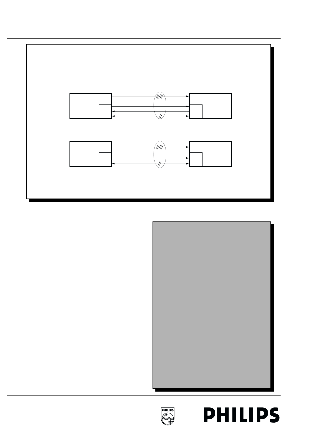
1. Introduction
CONFIGURATIONS
TV-CONFIGURATION
R, G, B, HS, VS
RECEIVER BOX
µP µP
MONITOR-CONFIGURATION
PERSONAL COMPUTER
µP µP
CONFIG_IDENT
DIS_RC_5
UART
R, G, B, H, V
CONFIG_IDENT
DDC
DISPLAY BOX
DISPLAY BOX
The successor of the FTV1.5 is the FTV1.9, which had to be
cheaper,and had to make as much as possible "re-use" of
PWB's from the FTV1.5.
It is built around an E-Box (= Receiver Box) and a 42" Monitor
(= Display Box). Within the Monitor a Fujitsu Plasma Display
panel - version 5 - is used.
For the FTV1.9, the Monitor can be used in two applications.
• Stand-alone configuration, monitor is connected to a PC or
a laptop
• TV configuration, where the monitor is connected to the Ebox.
The Monitor is a separate device, which can also be sold and
serviced separately.
The monitor, as a stand-alone unit, can be serviced by using a
test pattern coming from the PDP-LIMESCO panel on the
monitor itself or via a PC/laptop by using ComPair via the
ComPair connector.
Personal notes
CL 96532069_002.eps
240899
FTV1.9 Family has been set up for Europe, USA, Asian and
LATAM markets.
The Europe type consisting of 1 version, having no diversity.
FTV1.9DE Display Box 1. Introduction 3
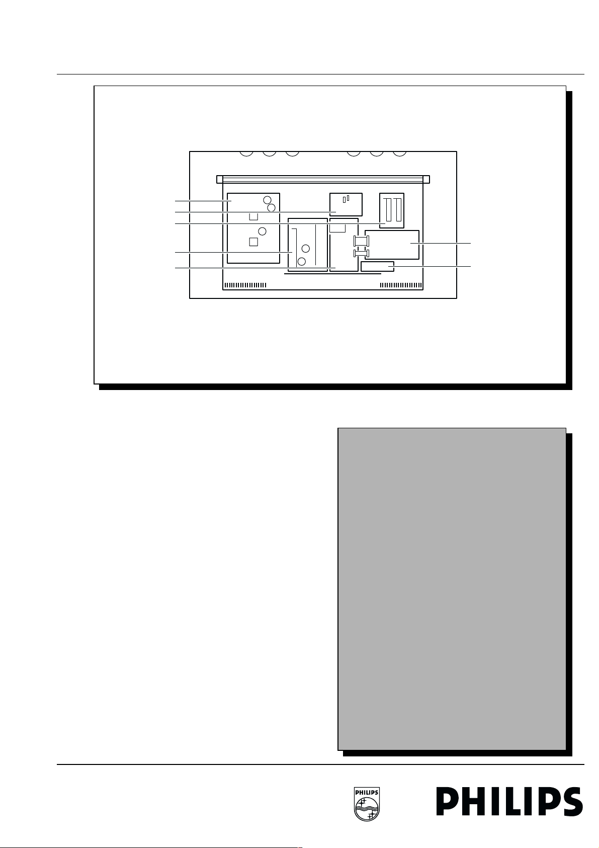
1.1 Description of used panels
1.1 Description of used panels
VS/VA Supply
PDP Discharge
Audio Amplifier
Pre-conditioner
AV Control
The panels are:
1. VsVa supply. At this panel all the supply voltages will be
generated for the display itself, the electronics of the display
and our PCB's. This panel contains also the fan control and
the protection circuits.
2. PDP Discharge Panel. Temporarily used in the DEMmodels of the FTV1.9. In the final models this panel is either
going to be integrated into the VsVa panel or is going to be
re-designed as a separate new panel. The function of this
panel is to discharge the big capacitor of the Vs-supply and
the Va-supply (minor reason). If these capacitors are not
discharged it can take up to 60 seconds before the set restarts after turning it OFF and ON again.
3. Audio amplifier. This panel is almost the same as the GFL
audio amplifier. Some small changes have been made like
other plugs, deleting a switch and external speaker
connectors and an adaptation of the outlines, just to mount
the panel at the backside of the Monitor.
4. Preconditioner. At this panel the mains input and mains
output (to connect the E-Box) is located. After the mains
input, the mains filter is placed. The panel contains also the
preconditioner. This is an auto voltage function from 95V ...
264VAC in to 380VDC out and the standby supply for the
P and the NVM.
µ
5. AV Control. At this panel the VGA, audio and control (UART
or DDC) signals enter the Monitor. These signals will be
buffered and are available at the output of this panel for
feedthrough (except the control signals). The same signals
will be fed to the Audio part (including an (optional) audio
CL 96532069_131.EPS
Personal notes
PDP Limesco
YUV/YC Input
120899

4 1. Introduction FTV1.9DE Display Box
1.1 Description of used panels
delay to correct the timing between video and audio) and to
the video control IC to control the RGB signals. Also the µP
for the panel control in the Monitor is located on this board.
The audio filters for the high and low/medium signals are
also located on the AV Control board.
6. PDP LIMESCO. This panel converts the analogue video
after gamma correction to a digital video signal, which is
connected to the PDP itself. The OSD generator is located
at the PDP LIMESCO, close to the LIMESCO IC for the
insertion of digital OSD information. The LIMESCO IC is
responsible for the scaling of the signals of the various
standard TV standards, VGA formats at this board. The H
and V position is corrected by an EPLD.
7. YUV YC input panel. This board gives the possibility to
attach several video formats to the stand-alone display. It
also has one stereo audio connection.
• Video input signals:
– YUV on three CINCHES (Y, Cb, Cr).
– YC on Hosiden connector (SVHS).
– CVBS on CINCH.
– CVBS on BNC.
• Audio input signals:
– L and R on 2 CINCHES.
• Output signal (AV Control):
– RBG-signal.
– H-sync and Vsync signal.
– L and R audio signal.
8. LED Display panel. At this panel, the LED's and the IRReceiver is located.
9. Switch Display panel. At this panel, the low power mains
switch is located. With this switch a relay is controlled to
switch ON and OFF the monitor
Personal notes
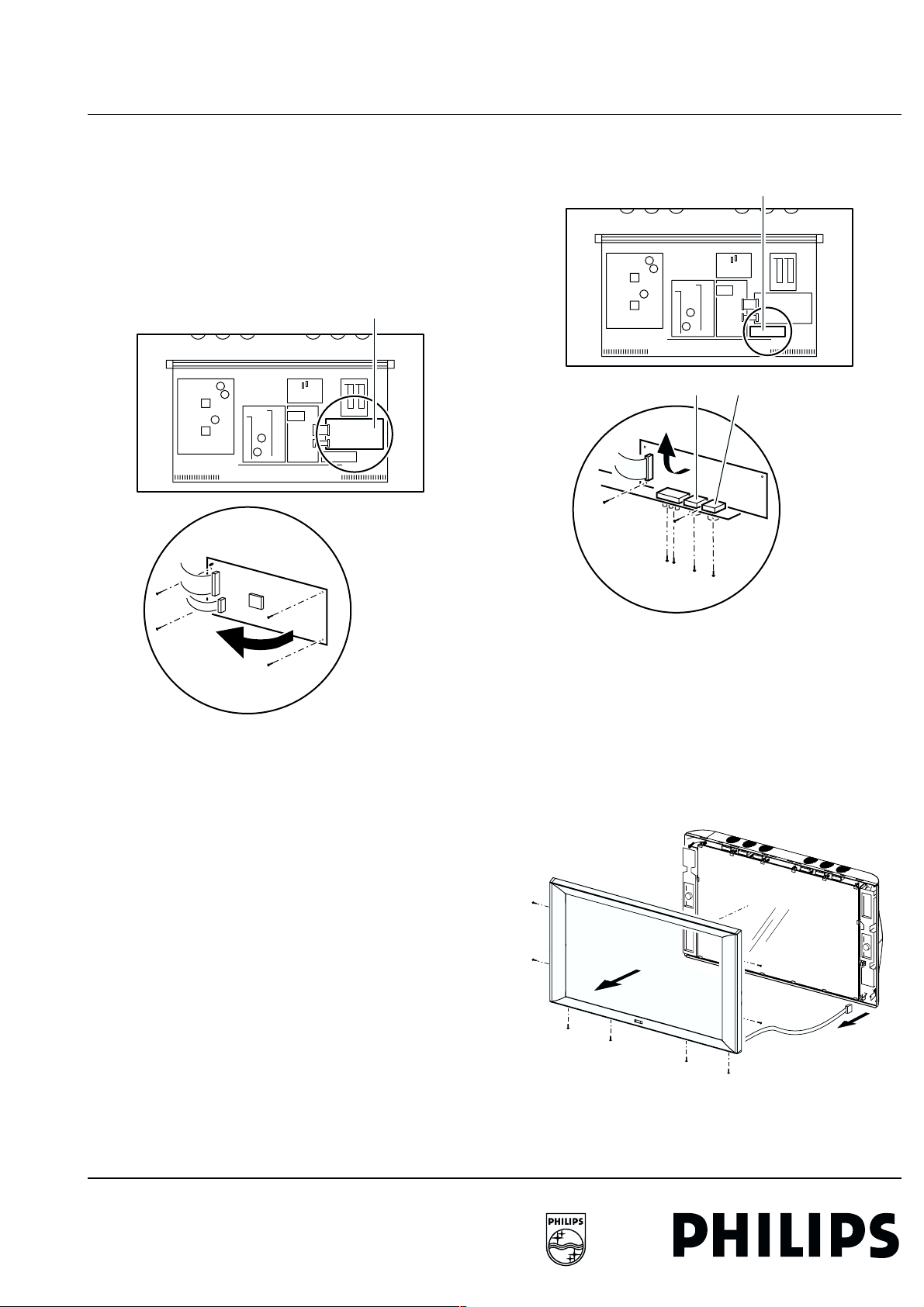
FTV1.9DE Display Box 2. Mechanical instructions 5
CL 96532069_132.EPS
120899
1
2
3
4
VS/VA Supply
FD07
2.1 Introduction:
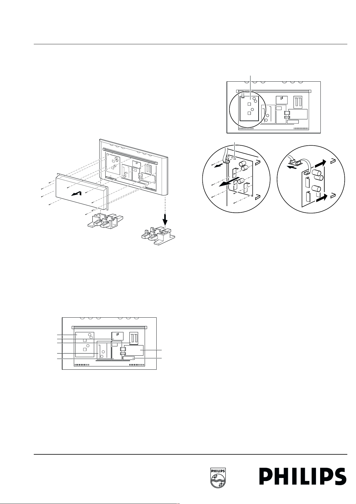
2. Mechanical instruction s2.1Introduction:
There are pre-defined service positions for the following panels:
1. VS/VA SUPPLY panel.
2. PDP DISCHARGE panel.
3. AUDIO AMPLIFIER panel.
4. PRE-CONDITIONER panel.
5. AV CONTROL panel.
6. PDP LIMESCO panel.
7. YUV/YC INPUT panel.
8. LED DISPLAY panel.
9. SWITCH DISPLAY panel.
Before these panels can be accessed, the rear cover has to be
removed:
2
VS/VA SUPPLY panel.
1
CL 96532069_130.EPS
120899
Figure 2-1
1. Place the Display Box in the service stand via 2 reinforced
cushions (order code: 3122 126 30181).
2. Remove the 9 fixation screws of the rear cover.
3. Remove the rear cover (during removal push it slightly
upwards).
VS/VA Supply
PDP Discharge
Audio Amplifier
Pre-conditioner
AV Control
CL 96532069_131.EPS
Figure 2-2
PDP Limesco
YUV/YC Input
120899
Figure 2-3
1. Disconnect Fan Supply cable from connector FD07 in the
upper left corner [1].
2. Remove the 7 fixation screws of the panel [2].
3. Place panel on the 2 hinges, which are located near the
right corners of the panel [3].
4. Use the mechanical service part (extension cable
assembly, 12NC: 3122 785 90006) to extend the Fan
Supply cable [4].
5. The copper side is now accessible from the left.
PDP DISCHARGE panel.
As in the FTV 1.5, this panel must be exchanged completely if
defective.
1. All panels are now accessible.
6 2. Mechanical instructions FTV1.9DE Display Box
2.1 Introduction:
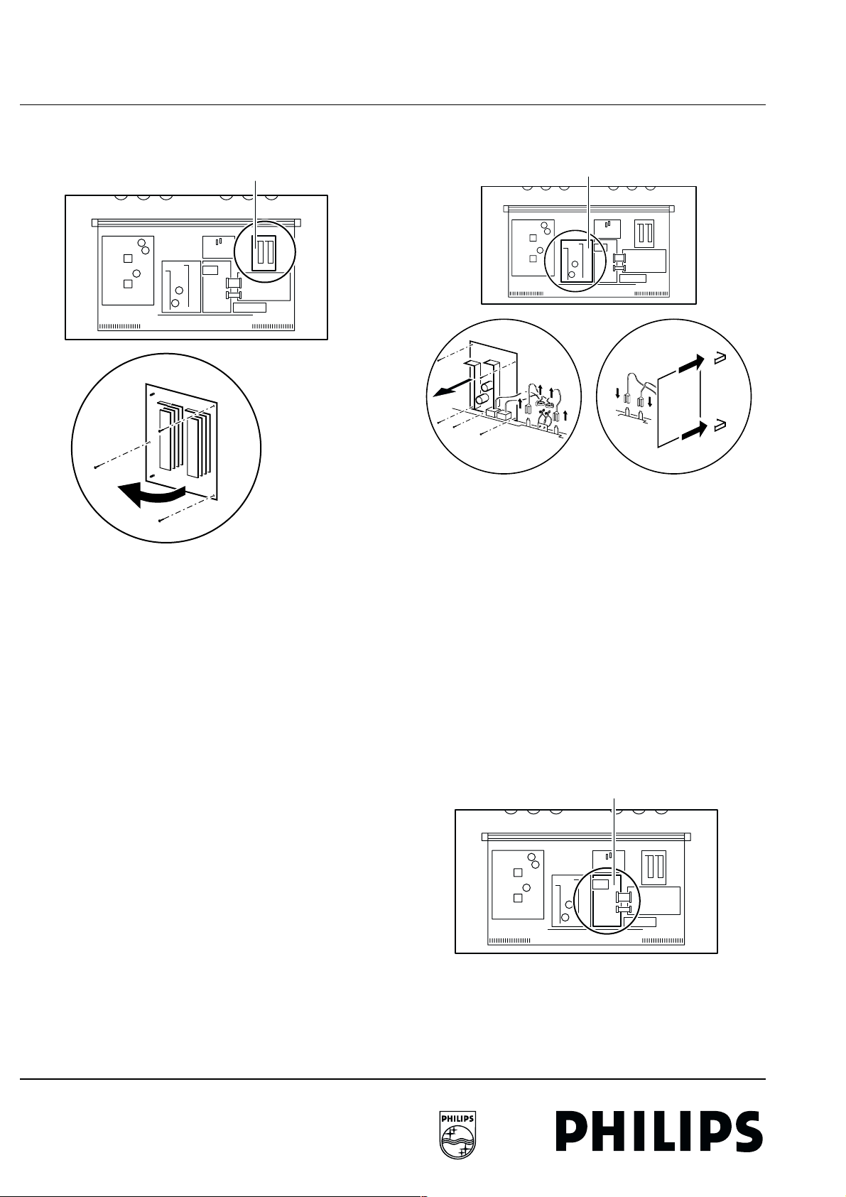
AUDIO AMPLIFIER panel.
Audio Amplifier
1
2
3
2
Figure 2-4
1. Some testpoints are accessible at the B-side [1].
2. If this is not sufficient, remove the 3 fixation screws of the
panel [2].
3. Panel now can be hinged on the left side to access the Aside (soldering side) [3].
CL 96532069_134.EPS
120899
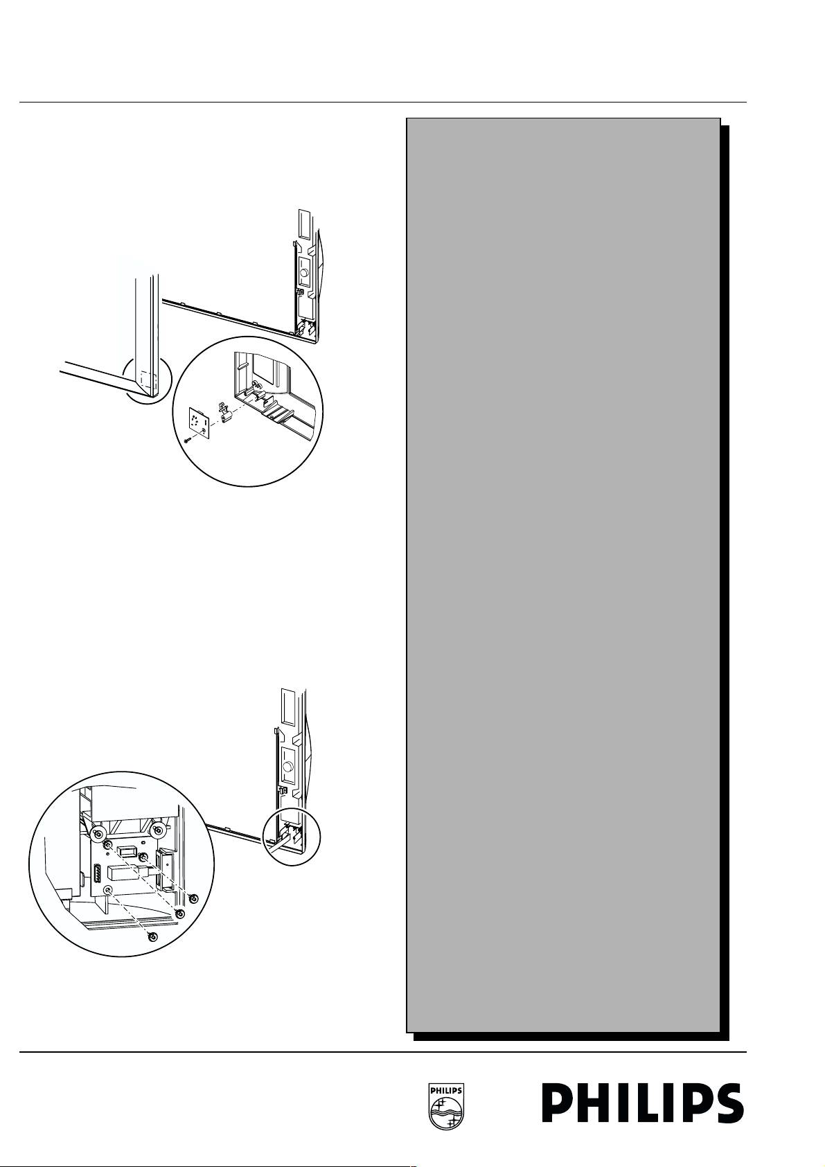
PRECONDITIONER panel.
Pre-conditioner
4
3
1
2
2
1
Figure 2-5
5
5
5
4
CL 96532069_135.EPS
120899
1. Disconnect the 2 grounding wires from the shielding plate
by pressing the small lever on the connector while pulling
[1].
2. Remove the 2 ferrite ring cores from their fixations [2].
3. Remove the 5 fixation screws of the panel [3].
4. Place panel on the 2 hinges, which are located, near the left
corners of the panel [4].
5. Reconnect grounding wires to the extra connectors on the
shielding plate at the left side [5].
6. The copperside becomes accessible now from the right
side.
AUDIO VIDEO CONTROL panel.
AV Control
Figure 2-6
CL 96532069_136.EPS
120899
FTV1.9DE Display Box 2. Mechanical instructions 7
YUV/YC Input
2
1
3
CL 96532069_138.EPS
120899
SVHS BNC
2
CL 96532069_139.EPS
120899
1
2
2
2.1 Introduction:
This panel has no service position for accessing the A-side,
however all service test points are accessible at the B-side (see
Service Manual).
In case some components must be (de)soldered, all fixation
screws (6 for the panel, 5 at the metal connector plate) and all
cables must be removed to access the A-side.
PDP LIMESCO panel.
PDP Limesco
YUV/YC INPUT panel.
1
1
1
2
1
CL 96532069_137.EPS
Figure 2-7
All SMC's are located on the B-side, so all testpoints are
accessible. In case some components must be (de)soldered,
the hinge construction can be used to access the A-side.
1. Remove the 4 fixation screws of the panel [1].
2. Panel can now be hinged to access soldering side [2].
120899
Figure 2-8
This panel has no pre-defined service position. For access of
the A-side, the panel has to be removed:
1. Remove the 4 screws at the metal connector plate [1].
2. Remove the 2 fixation screws of the panel [2].
3. Panel can be removed now to access the A-side [3].
LED DISPLAY panel.
Figure 2-9
8 2. Mechanical instructions FTV1.9DE Display Box
2.1 Introduction:
1. Remove 2 x 2 screws at the sides and 4 screws at the
bottom of the front cover [1].
2. Remove the front cover (it hinges at the top). During
removal unplug the cable of the LED DISPLAY panel at the
SWITCH DISPLAY panel (connector SD11) [2].
3
Personal notes
CL 96532069_140.EPS
Figure 2-10
120899
1. The LED DISPLAY panel can be removed now by
unscrewing 1 fixation screw [3].
SWITCH DISPLAY panel.
1. Remove front cover (for a description see Chapter 2.1.8
'LED DISPLAY panel').
3
CL 96532069_141.EPS
Figure 2-11
120899
1. The SWITCH DISPLAY panel can be removed now by
unscrewing 3 fixation screws [3].
FTV1.9DE Display Box 2. Mechanical instructions 9
CL 96532069_143.EPS
120899
3
3
3
3
4
4
2.2 Exchanging parts
2.2 Exchanging p arts
Some parts of the FTV1.9 Display Box must be exchanged if
defective:
1. GLASS PLATE.
2. LOUDSPEAKER.
3. PLASMA DISPLAY PANEL [PDP].
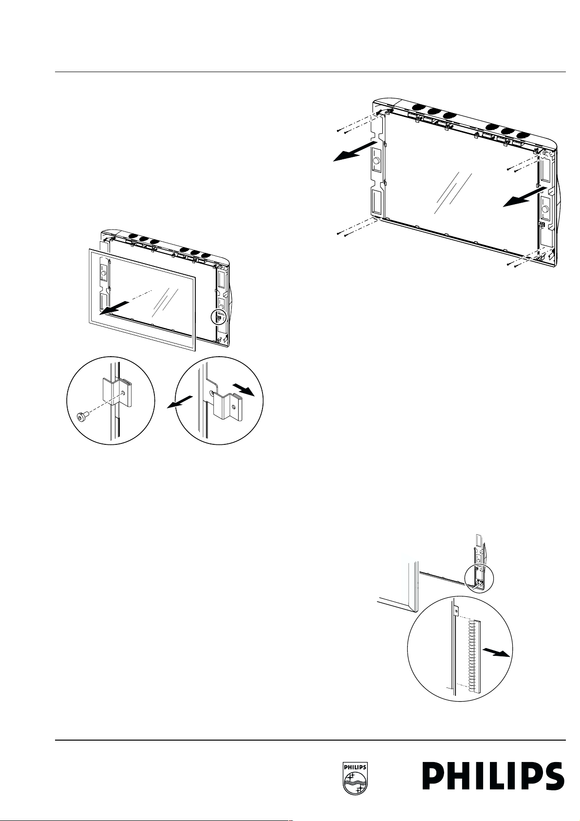
Exchanging of the GLASS PLATE.
1. First unplug (remove Mains and VGA cable) the Display
Box .
2. Remove front cover (for a description see Chapter 2.1.8
'LED DISPLAY panel').
2
5
34
CL 96532069_142.EPS
Figure 2-12
120899
1. Now the GLASS PLATE can be removed by unscrewing all
screws [3] and removing all glass clips [4].
Exchanging of a LOUDSPEAKER.
1. First unplug (remove Mains and VGA cable) the Display
Box.
2. Remove front cover (for a description see Chapter 2.1.8
'LED DISPLAY panel').
Figure 2-13
1. The LOUDSPEAKER can now be removed by
disconnecting its cable and removing the 4 fixation screws
at the top and bottom of the speakerbox. Be sure to remove
the correct screws, otherwise the speaker system will be
damaged (it is an airtight system).
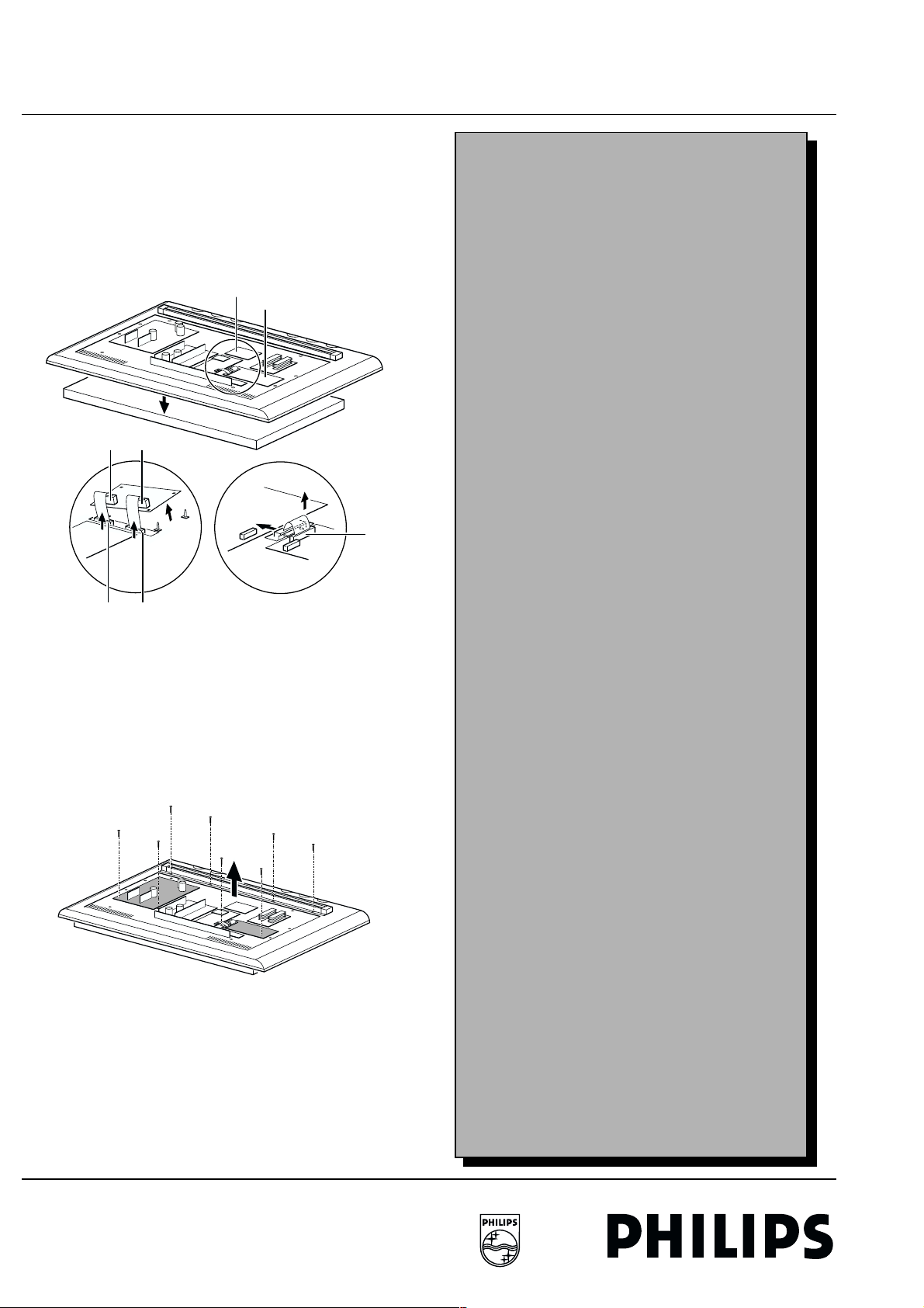
Exchanging of the PDP.
1. First unplug (remove Mains and VGA cable) the Display
Box.
2. Place the rear side of the Display Box on a foam cushion (be
sure the metal rear cover is mounted in order to prevent
damaging of the electronic panels).
3. Remove front cover (for a description see Chapter 2.1.8
LED DISPLAY panel).
4. Now the GLASS PLATE can be removed by unscrewing all
screws and removing all glass clips (for a description see
Chapter 2.2.1. 'Exchanging of the GLASS PLATE').
Figure 2-14
6
CL 96532069_144.EPS
120899
10 2. Mechanical instructions FTV1.9DE Display Box
2.2 Exchanging parts
1. Remove all copper EMC SHIELDING springs mounted
around the display [6].
2. Now flip the complete Display Box and place it with the
Plasma Display down on a foam cushion. Be 100 % sure a
large foam cushion is placed underneath the PDP, as it will
drop about 10 mm after removing its fixation screws ! !
3. Disassemble metal rear cover (for a description see
Chapter 1.1 'Introduction').
PDP Discharge
PDP Limesco
FOAM CUSHION
1
FD173 FD171
Personal notes
4
CL 96532069_145.EPS
3
CN24
2
5
3
CN23
Figure 2-15
1. Disconnect the following cables:
– Cables coming from connectors CN23 and CN24 of the
PDP DISPLAY panel [3] (for easiest access lift the PDP
DISCHARGE panel from its fixations [2]).
– Flat cable on connector PD3 of the PDP LIMESCO
panel [4]. Also remove the ferrite 'flat cable shield'
completely by unlocking its fixations [5].
1
2
2
1
1
3
2
2
1
PD3
120899
CL 96532069_146.EPS
120899
Figure 2-16
1. Now remove the 8 large screws which hold the PDP:
– 4 screws are located at the top: they also hold the
aluminium wall mount [1].
– The other 4 are located at the bottom: the 2 outer screws
are hidden behind panels. Therefor unscrew the VS/VA
SUPPLY and the PDP-LIMESCO panel (grey panels)
[2].
2. Lift encasing from PDP and replace PDP [3].

FTV1.9DE Display Box 3. Block diagram 11
3. Block diagram
For the block diagram see Service Manual chapter 6.
The power is supplied by the VsVa supply (which is an LLC
converter). The Pre-conditioner delivers the input voltage of
380 V.
The output voltages of the VsVa supply are:
• Va: 55 V + 5 * Vra (Vra varies between 0 and 2 V).
• Vs: 165 V + 10 * Vrs (Vrs varies between 0 and 2 V).
• +5 V, 8.6 V and the +/- V_audio.
The controls located on the µP panel, which is a panel on the
AV Control panel, are activated by the keyboard on the Front I/
O and RC5 signals from the remote control receiver on the LED
panel.
Audio signals coming from the YUV Y/C panel or from the AV
Control are selected and processed at IC7940 (TDA9860). The
outcoming L/R signals are filtered (HPF) and corrected for low
frequency by the DBE-circuit, before they are fed to the Audio
amplifier.
CVBS signals (BNC connector or CINCH) at the YUV Y/C panel
are first passed through a comb-filter IC7012. The output
signals (Y and C) of IC7012 and the Y/C signal from the SVHS
connector are selected by IC7010. The output Y/C are fed to
YUV/RGB matrix IC7013 (TDA8854).
The YUV signals (CINCH) are processed separately in a RGB
matrix and transferred to IC7013. The selected RGB_YC output
signals from IC7013 are fed to the AV Control panel.
RGB signals coming from the Receiver Box or PC, the normal
RGB_VGA or separate RGB_YC signals are selected by the
source select switch (IC7360). The output signals are fed to the
video control IC7300. The RGB output signals from IC7300 are
buffered and transferred to the PDP LIMESCO panel. Here the
signals are prepared and processed (gamma correction;
filtered; digitised by an ADC), buffered and fed to the display.
OSD-signals are added on the display via the PDP LIMESCO
IC.
RGB_VGA input signal are buffered and passed through to the
VGA-out connector.
Personal notes

12 4. Service modes FTV1.9DE Display Box
2.2 Exchanging parts
4. Service modes
For the FTV1.9, the Monitor can be used in two applications.
• A stand-alone configuration, a separate device which can
also be sold and serviced separately.
• TV configuration, where the monitor is combined with the Ebox.
The monitor, as a stand-alone unit, can be serviced by using a
test pattern coming from the PDP-LIMESCO panel on the rear
of the monitor itself or via a PC/laptop by using ComPair via the
ComPair connector.
In this chapter the following paragraphs are included:
1. Test points
2. Dealer Service Tool (DST)
3. Service Modes
4. Error code buffer and error codes
5. The "blinking LED" procedure
6. Fault-finding tips
7. ComPair
Personal notes

FTV1.9DE Display Box 4. Service modes 13
4.1 Test points
4.1 Test poi nts
The FTV1.9 chassis is equipped with test points in the service
printing. These test points are referring to the functional blocks:
• A1-A2-A3, etc.: Test points for the Audio amplifier (A)
• C1-C2-C3, etc.: Test points for the AV control circuit (AVC)
• FD1-FD2-FD3, etc.: Test points for the VsVa supply (FD1FD2) and the PDP discharge panel
• L1-L2-L3, etc.: Test points for the PDP LIMESCO (PD1PD9)
• PR1-PR2-PR3, etc.: Test points for the Pre-conditioner
(PR1-PR3)
• Y1-Y2-Y3, etc: Test points for the Y/C YUV monitor panel
(UY1-YC4)
Measurements are performed under the following conditions:
Video: colour bar signal; Audio: 3 kHz left, 1 kHz right
Personal notes

14 4. Service modes FTV1.9DE Display Box
4.2 Dealer Service Tool (DST)
4.2 Dealer Service Tool (DST)
For easy installation and diagnosis the dealer service tool
(DST) RC7150 can be used. When there is no picture (to
access the error code buffer via the OSD), DST can enable the
functionality of displaying the contents of the entire error code
buffer via the blinking LED procedure, see also paragraph 5.5.
The ordering number of the DST (RC7150) is 4822 218 21232.
Installation features for the dealer
The dealer can use the RC7150 for programming the TV-set
with pre-sets. 10 Different program tables can be programmed
into the DST via a GFL TV-set (downloading from the GFL to
the DST; see GFL service manuals) or by the DST-I (DST
interface; ordering code 4822 218 21277). For explanation of
the installation features of the DST, the directions for use of the
DST are recommended (For the FTV1.9 chassis, download
code 4 should be used).
Diagnose features for service
FTV1.9 sets can be put in two service modes via the RC7150.
These are the Service Default Mode (SDM) and the Service
Alignment Mode (SAM).
Personal notes

FTV1.9DE Display Box 4. Service modes 15
4.3 Service Modes
4.3 Service Modes
Below described sequence is only valid for the "Monitor Only
Configuration". When a Receiver box is connected to the
Display Box (TV Configuration), please check chapter 4 in the
Training Manual of the Receiver Box.
Service Default Mode (SDM)
The purpose of the SDM is:
• Provide a situation with predefined settings to get the same
measurements as in this manual.
• Access to the error buffer via the blinking LED procedure.
• Inspect the error buffer.
• Possibility to overrule software protections via the service
pins (caution: override of software protections! ).
Entering the SDM:
• By transmitting the "DEFAULT" command with the RC7150
Dealer Service Tool (this works both while the set is in
normal operation mode or in the SAM).
• By pressing on a standard RC the following sequence 0, 6,
2, 5, 9, 6 followed by the "MENU" key.
• By short-circuiting the SDM pin on the µP panel.
In the SDM the following information is displayed on the screen:
--------------------------------------------------------------
F19DBC X.Y_12345 (1) LLLL (2) SDM (3)
ERR 02 01 14 ## ## ## ## ## ## ##
--------------------------------------------------------------
Explanation notes/references:
(1) Software identification of the main micro controller (F19DBC
X.Y_12345)
• F19D is the chassis name for FTV1.9 display
• B is the region identification
• C is the language cluster
• X = (main version number)
• Y = (subversion number)
• ##### are 5 digits of the Serial number
(2) "LLLL" Normal display operation in hours
(3) "SDM" To indicate that the TV set is in the service default
mode
(4) "ERR 02 01 14 ## ## ## ## ## ## ##" This line shows the
contents of the error buffer (max. 10 errors). The last error that
occurred is displayed at the most left position. When less then
10 errors have occurred the rest of the line is empty. When the
errorlist is empty " No errors" is displayed. No duplicate errors.
Exit the SDM:
Push the "Standby" button on the Remote Control.
The SDM sets the following pre-defined conditions:
• Volume level is set to 25% (of the maximum volume level).
• Linear Audio and Video settings are set to 50%.
• Colour temperature is set to normal.
The following functions are "overruled" in SDM since they
interfere with diagnosing/repairing a set
• Video blanking.
• Slow demute.
• Anti-ageing.
• Automatic switch to "Standby" when H- and/or V-sync
signals are lost.
All other controls operate normally.
Service Alignment Mode (SAM)
The purpose of the SAM is to align and or adjust settings.
For recognition of the SAM, "SAM" is displayed at the top of the
right side of the screen
Entering the SAM-menu:
• By pressing the "ALIGN" button on the RC7150 Dealer
Service Tool
• Standard RC sequence 062596 followed by the "OSD"
button.
• By short-circuiting the SAM pin on the µP panel (Caution:
override of software protections ! ! )
In the SAM the following information is displayed on the screen:
--------------------------------------------------
F19DBC X.Y_12345 SAM
ERROR## ## ## ## ##
WHITE POINT
PDP TEST PATTERN [ON/OFF]
STORE
RESET ERROR BUFFER
--------------------------------------------------
The menus and submenus
White point
The white point sub menu contains the following items:
•RED
• GREEN
•BLUE
• COLOUR TEMPERATURE
PDP Test pattern
By selecting this item, all OSD disappears from the screen. The
screen now changes from light grey to dark grey in a slow
regular rhythm. One can so easily check if all pixels of the
monitor are correct.
Store
The change values are stored in the NVM.
Reset Error Buffer
This option will reset the error buffer.
Exit the SAM:
Push the "Standby" button on the Remote Control.
SAM menu control:
Menu items can be selected with the "UP" or "DOWN" key.
Entry into the selected items (sub menus) is done by the "LEFT"
or "RIGHT" key. The selected item will be highlighted.
With the same "LEFT/RIGHT" keys, it is possible to increase/
decrease the value of the selected item.
Return to the former screen by pushing the "MENU" button. The
item values are stored in NVM if the sub menu is left.

16 4. Service modes FTV1.9DE Display Box
4.3 Service Modes
Customer Service Mode (CSM) Display
FTV1.9 monitors are equipped with the "Customer Service
Mode" (CSM). CSM is a special service mode that can be
activated and de-activated by the customer, upon request of
the service technician/dealer during a telephone conversation
in order to identify the status of the set. This CSM is a 'read only'
mode, therefore modifications in this mode are not possible.
Entering the Customer Service Mode.
• By pressing on RC03333/01 the following sequence :
Picture, sound, cursor up, cursor down, cursor left, cursor
right followed by the button (MUTE)
Exit the Customer Service Mode.
• pressing the "MENU" or any key on the Remote Control
handset (except "P+" or "P-")
• switching off the TV set with the mains switch.
All settings that were changed at activation of CSM are set back
to the initial values
The Customer Service Mode information screen
Personal notes
The following information is displayed on screen:
--------------------------------------------------
CUSTOMER SERVICE MENU
• Software version F19DBC X.Y_#####)
• Code 1: contains the last 5 error codes
• Code 2: contains the first 5 error codes with the last
received error at the most left-hand side.
• Service unfriendly modes
--------------------------------------------------
FTV1.9DE Display Box 4. Service modes 17
4.4 Error code buffer and error-codes
4.4 Error code buffer and error-codes
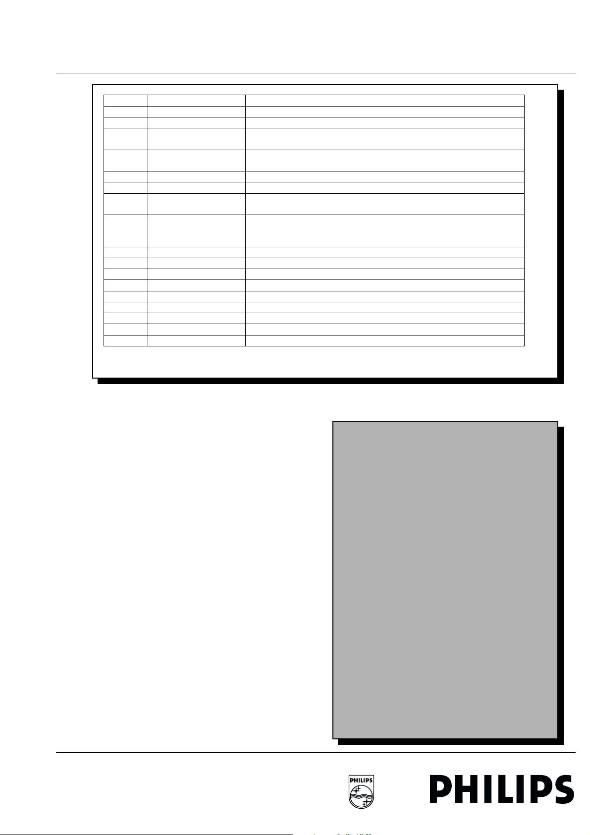
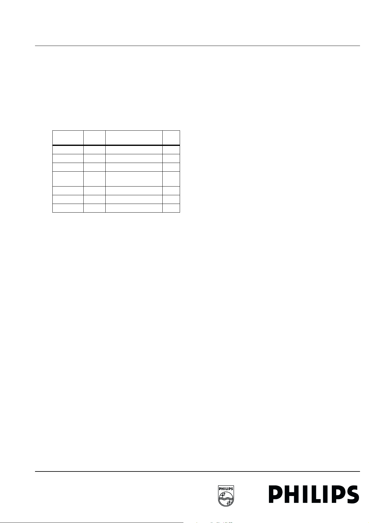
Error-nr Type of Error Possible defect/cause
1 +5V
2 8V6
3 Fan_prot Gives an indication that 1 or more FAN(s) does not function, or that 1 or
4 Over-temp_prot Temperature at the heatsink of the VsVa supply or the Preconditioner is
5 DC_prot Audio-amplifier IC, its supply or the Audio amplifier is defect
6 Over_voltage_prot Vs or Va supply voltage is too high
7 Vrr Powersupply of the display is not correct. Ignorance of the signal during
8 Power_OKE Power supply or modules that uses this voltage. If this signal is NOT
9 Blocked NVM IIC bus NVM IIC bus is not correct
10 Blocked slow IIC bus Slow IIC bus is not correct
11 TDA9860 No acknowledge of Audio controller
12 TDA4885 No acknowledge of Video controller
13 MC141585 No acknowledge of OSD Generator
14 uPD93687GD-LBD No acknowledge of Limesco
15 PCF8574AT No acknowledge of I/O Expander
16 NVM No acknowledge of NVM
17 Communication Fault in the communication
Figure 1 : Error-code list of the D-box
+5V pin at uP is low.
8V6 pin at uP is low
more fan control circuits is defect
too high
startup by the software.
activated means that all supply voltages are available (exception Audio
supply )
ch5-table1-mon.eps
041099
The error code buffer contains all errors detected since the last
time the buffer was erased. The buffer is written from left to
right.
In case of non-intermittent faults, clear the error buffer before
starting the repair to prevent that "old" error codes are present.
If possible check the entire content of the error buffers. In some
situations an error code is only the RESULT of another error
code (and not the actual cause).
Note: a fault in the protection detection circuitry can also lead to
a protection
The error code buffer will be cleared in the following cases:
• exiting SDM or SAM with the "Standby" command on the
remote control
• transmitting the commands "DIAGNOSE-9-9-OK" with the
DST.
The error buffer is not reset by leaving SDM or SAM with the
mains switch.
Examples:
ERROR: 0 0 0 0 0 : No errors detected
ERROR: 6 0 0 0 0 : Error code 6 is the last and only detected
error
ERROR: 5 6 0 0 0 : Error code 6 was first detected and error
code 5 is the last detected (newest) error
Personal notes

18 4. Service modes FTV1.9DE Display Box
4.5 The "blinking LED" procedure
4.5 The "blink ing LED" procedu re
The contents of the error buffer can also be made visible
through the "blinking LED" procedure. This is especially useful
when there is no picture.
There are two methods:
• When the SDM is entered, the LED will blink the contents of
the error-buffer. Error-codes = 10 are shown as followed. A
long blink of 1second which is an indication of the decimal
digit, followed by a pause, followed by n short blinks. When
all the error-codes are displayed, the sequence is finished
with a led display of about 3 seconds. The sequence starts
again.
• With the DST all error codes in the error buffer can be made
visible. Transmit the command: "DIAGNOSE x OK" where x
is the position in the error buffer to be made visible x ranges
from 1, (the last (actual) error) to 10 (the first error). The
LED will operate in the same way as in the previous point,
but now for the error code on position x.
Example:
Error code position 1 2 3 4 5
Error buffer: 12 9 5 0 0
• after entering SDM: 1 long blink of 1 sec. + 2 short blinks pause - 9 short blinks - pause - 5 short blinks - pause long blink of 3 sec. --etc.
• after transmitting "DIAGNOSE- 1- OK" with the DST: 1 long
blink 2 short blinks - pause - 1 long blink + 2 short blinks etc.
• after transmitting "DIAGNOSE- 2- OK" with the DST: blink
(9x) - pause - blink (9x) - etc.
• after transmitting "DIAGNOSE- 3- OK" with the DST: blink
(5x) - pause - blink (5x) - etc.
• after transmitting "DIAGNOSE- 4- OK" with the DST:
nothing happens
Personal notes
FTV1.9DE Display Box 4. Service modes 19
4.6 Protections
4.6 Protections
All protections are handled by the hardware. The SW will only
monitor the hardware to generate error codes for the service.
The hardware switches to protection when one of the following
protections becomes active: FAN_PROT,
OVER_TEMP_PROT, DC_PROT, OVER_VOLTAGE_PROT
and Vrr.
When 1 of these protections occur, the HW will switch the set
to STANDBY.
The error must be read out by the microprocessor and the error
code must be generated. The microprocessor keeps the set in
STANDBY and starts the blinking red led. It is not allowed to
start up as long as the protections are present.
For the error code generation, the following levels of the A/D
converter are defined:
Input voltage at A/D converter [V]: Sort protection:
< 0.300 V No protection
0.3 < V < 1.875 FAN_PROT
1.875 < V < 2.813 OVER_VOLTAGE_PROT
2.813 < V < 3.75 OVER_TEMP_PROT
3.75 < V < 4.688 DC_PROT
Personal notes
20 4. Service modes FTV1.9DE Display Box
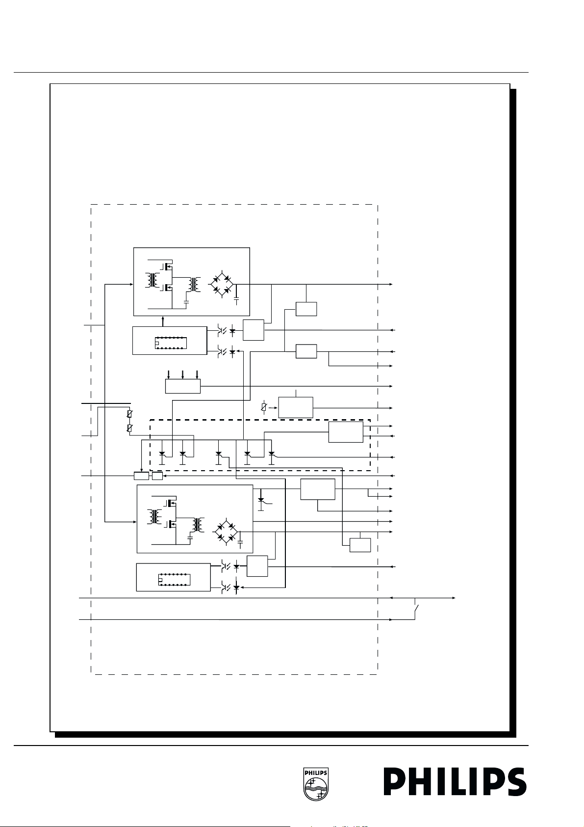
DISPLAY SUPPLY MODULE
LLC Converter
Vs
OVP
380 V
DC
LLC Control
Error
Amp.
SENSE
Vrs
TEMP
Voc
ok
Vs Va
POWER OK
ptc
ptc
Vs OVP
AND -1
Protection
Circuit
Va OVP
LLC Converter
LLC Control
ptc
Fan
Protect
Error
Amp.
5V OVP
Delay
17V
FAN
PROTECTION
17V
DC_DC
Converter
OVP
SENSE
Vrr
Vrr to µP
POWER OK
Fans (1-5)Speed Control
FAN PROT
PROT-FAN (1-5)
DC PROT (Audio)
STBY
+5V
Vcc
+8V6
+/- V Audio
Va
Vra
5VSTBY-SWITCHED
On/Off
Switch
5VSTBY
TO µP
CL 96532069_112.eps
240899

FTV1.9DE Display Box 4. Service modes 21
4.6 Protections
POWER_OKE
For ease of start-up and fault diagnosis a POWER_OKE signal
is generated. The signal is high when the voltages that are
sensed are in the right level. This signal is mixed with signals
derived from Vs and the Va. The POWER_OKE signal will be
high when simultaneously:
5V = 5V
17V >12.8V
Vs >135V
Va > 45V
In all other cases the output is low.
Personal notes
22 4. Service modes FTV1.9DE Display Box
4.6 Protections
5VSTBY-SWITCHED
VCC
VDD
+5V
7301
CONNECTOR
D09
TEMP
45
3331
3332
3333
7371
7302
8
3
7330-A
2
4
7370
CONNECTOR
FD06-12
5VSTBY-SWITCHED
17V
7331
PROTECTION-STATUS
7332
SUPPLY-ON
[PR3]
7337
2134
3339
3379 3378
5VSTBY-SWITCHED
VA
3136
3135
3133
7113
7112
3137
3134
3138
3386
3323
3380
5VSTBY-SWITCHED
5VSTBY-SWITCHED
7339
3384
7341
3385
7114
3394
21352132
7314
PROTS
7333
7321
DC
6371
3039
7003 7103
7340
7338
VS
5VSTBY-SWITCHED
3033
3058
3034
2037
FD1
[C-14]
AA
7315
3011
7001-PIN10
2038
PROT-FAN 1-6
17V
3139
7103
3111
7101-PIN10
3035
7012
7013
3038
7316-7321
CL 96532058_086.eps
3036
7016
3037
2032
280999
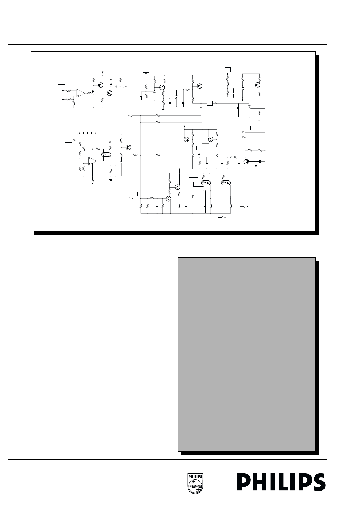
Protection structure
The protection structure of the FTV1.9 D-box is shown at figure
above.
The FTV1.9 monitor has one microprocessor, which is situated
on the AV-control panel and is supplied by the 5V standbysupply. The microprocessor is even active when the set is
switched to standby. The microprocessor controls the "supplyon" line which switches first relay 5680 and then relay 5690.
In de standby-mode or the protection-mode the "supply-on" line
is "low" and both both relays are switched off. The
preconditioner is disconnected from the mains.
The potections of the FTV1.9 monitor can be divided into 5
subgroups:
– Fan_prot
– Over_temp_prot
– DC_prot
– Over_voltage_prot
–Vrr
For the Fan-, Over_temp, DC and the Over_voltage protections
the signals for the µP are latching, using the 5Vstby_switched
for powering the circuits permanently. The µP has sufficient
time for diagnosis and for storing the error-codes in the NVM.
Vrr, which is an indication of the powersupply of the display is
correct, is directly fed to the µP.
Personal notes
FTV1.9DE Display Box 4. Service modes 23
4.6 Protections
Signal line "PROTECTION STATUS" and errorcodes
When one of the protection mechanism is triggered, the
5Vstby-switched is connected via a saturated transistor and a
pre-defined resistor to signal line "protection status", which is
connected to the µP.
Signal line "protection status" is connected to ground via
resistor R3378 and 3379. For each seperate fault condition
mechanism we get a pre-defined voltage at the
µΠ.
This results in the following table
Protectionmode
None ----- < 0.3V none
Fan_prot 1K
Vs or
Va_prot
Temp_prot 220
DC-prot 68
Vrr ------ ------ 7
Series
resistor
Ω
Ω
470
Ω
Ω
Voltage at "protectionstatus" line
0.30V < Vprot < 1.90V 3
1.90V < Vprot < 2.80V 4
2.80V < Vprot < 3.75V 5
3.75V < Vprot < 4.7V 6
Errorcode
Protection signal Vrr coming from the PDP, to indicate that the
powersupply is ok or not ok ( "1" or "0" ) is directly connected
to the µP. Error-code 7 is stored in the NVM and the set is
switched to standby.
When one of the protections is activated, the power supplies of
the Vs and Va are shut down and the set is switched to standby.
Fan protection
When this protection is activated, the Va- and Vs power supply
are shut down. The set is switched to the standby mode and
error-code 3 is stored in the NVM.
The fan voltage is powered by 17V, but clamped to 12V to
prevent damage. In order to be able to verify whether the fans
are running, a fault detection circuit is implemented for each of
the 6 fans. A running fan gives pulses in the same speed as the
rotation of the blades. The circuit uses these pulses to trigger
the discharge of an elcap. The elcap is continuously charged
through a resistor.
Example : Capacitor C2319 is charged through R3356 and at
every pulse discharged by T7322. When fan 6 is blocked,
C2314 is charged via D6326 en triggers thyristor 7315,
because C2319 is no longer discharged via T7322. The current
now flows from the 5Vstby-switched via resistor 3383 and 3325
driving transistor T7321 into saturation. The voltage "protection
status" is now determined by the voltage dividing of R3323 and
resistor R3378 and 3379. ( neglect the Vce of 0.2V of T7321. ).
Reset of the VsVa-supply.
Transistor T7339 is shorted now by the presence of the
"protection status" signal. T7339 connects resistor R3376 and
R3389 to ground, switching on T7338. Thyristor 7333 is now
triggered, shorting signal PROTS to ground. To follow the
signal flow, go to the right upper corner of schematic FD1.
Connecting PROTS to ground, will start a current flow through
opto-coupler diode 7103 and the opto-coupler transistor
connects supply voltage Vcc2 to the fault input ( pin 10 ) of IC
7101. When the voltage at pin 10 exceeds 1.0V, IC7101 stops
oscillating. The Va-supply stops functioning.
To continue the signal flow, go to the right upper corner of
schematic FD2. Connecting PROTS to ground also results in a
current flow through the opto-coupler diode of 7003. The optocoupler transistor connects supply voltage Vcc1 to the fault
input ( pin 10 ) of IC 7001. When the voltage at pin 10 exceeds
1.0V, IC7001 stops oscillating. The Vs-supply stops
functioning.
Vs and Va protection
Va protection
When this protection is activated, the Va- and Vs power supply
are shut down. The set is switched to the standby mode and
error-code 4 is stored in the NVM.
When the Va-supply exceeds the 68V, regulator 7112 is
triggered and will switch on T7113. Capacitor 2132 is charged
via the 5Vstby-switched and will trigger thyristor 7114, which
will switch on T7341. The voltage "protection status" is now
determined by the voltage dividing of R3386 and resistor
R3378 and 3379. ( neglect the Vce of 0.2V of T7341 ). See
schematic FD2.
The presence of the voltage at "protection status" line will
eventually reset the VsVa-supply. For more info see
subparagraph - Reset of the VsVa-supply.
Vs protection
When this protection is activated, the Vs power supply is shut
down. The set is switched to the standby mode and error-code
4 is stored in the NVM.
When the Vs supply exceeds the 198V, regulator 7012 is
triggered and will switch on T7016. Capacitor 2032 is charged
via the 5Vstby-switched and will trigger thyristor 7013. Thyristor
7013 is fired and connects signal Aa to ground. To follow the
signal flow, go to the right upper corner of schematic FD1.
When signal Aa is shorted to ground, T7341 is switched on. The
voltage "protection status" is now determined by the voltage
dividing of R3386 and resistor R3378 and 3379. ( neglect the
Vce of 0.2V of T7341 ). See schematic FD2.
The presence of the voltage at "protection status" line will
eventually reset the VsVa-supply. For more info see
subparagraph - Reset of the VsVa-supply.
Temperature Protection
When this protection is activated, the Va- and Vs power supply
are shut down. The set is switched to the standby mode and
error-code 5 is stored in the NVM.
When the temperture of the heatsink on the Preconditioner
panel or on one of the 2 heatsink on the VsVa panel exceeds
the 110°C, the PTC resistance increases drastically. The
voltage at pin 3 of IC7330 will drop and the output of 7330 will
do the same. The current flow through opto-coupler diode 7331
results also in a current flow through the opto-coupler transistor
and will trigger thyristor 7332. The fired thyristor switches
transistor 7337 on. The voltage "protection status" is now

24 4. Service modes FTV1.9DE Display Box
4.6 Protections
determined by the voltage dividing of R3339 and resistor
R3378 and 3379. ( neglect the Vce of 0.2V of T7337 ).
The presence of the voltage at "protection status" line will
eventually reset the VsVa-supply. For more info see
subparagraph - Reset of the VsVa-supply.
DC Protection - Audio Amplifier
When this protection is activated, the Va- and Vs power supply
are shut down. The set is switched to the standby mode and
error-code 6 is stored in the NVM.
In case of a fault in the Audio amplifier or when a DC voltage
appears on the speaker output, a signal called DCPROT is
generated. See schematic FD2 - F7. In case of a fault, thyristor
7314 is triggered and switches on T7340. The voltage
"protection status" is now determined by the voltage dividing of
R3380 and resistor R3378 and 3379. ( neglect the Vce of 0.2V
of T7340 ).
The presence of the voltage at "protection status" line will
eventually reset the VsVa-supply. For more info see
subparagraph - Reset of the VsVa-supply.
Vrr - PDP supplies
Personal notes
Vrr is a logical signal ( "high" in normal circumstances ) that
comes from the PDP. It's purpose is to trigger the switch off of
the Pre-conditioner supply in case Vrr becomes "low" , to trigger
the shutdown of the VsVa supply and to initialise that errorcode 7 is stored in the NVM.
When signal Vrr becomes "low", see FD1 - F13, the output of
IC7301-B becomes "high". This results in two actions.
It will trigger thyristor 7302 and short signal PROTS to ground.
This results eventually in a reset of the VsVa supply.
Switching on T7371, which again switches on T7370 via the
5Vstby-switched supply. Signal-line "supply-on" is now
grounded. This results in switching off relay 5680 and 5690,
disconnecting the mains from the pre-conditioner. The standby
supply( 5Vstby-switdhed ) is still functional.

FTV1.9DE Display Box 4. Service modes 25
4.7 Alignments
4.7 Alignment s
Electrical Alignments
Pre-conditioner +5Vstby (PR3)
Connect a voltmeter to capacitor C2510 (PR2). With the aid of
R3504 adjust the voltage to 5.2 V +/- 50 mV.
Va-supply (Addressing of the PDP - FD1)
De-activated the PDP.
Connect a voltmeter to capacitor C2120 (FD1). With the aid of
R3126 adjust the voltage to 55 V +/- 0.5 V.
Vs-supply (Sustain pulses - FD2)
De-activated the PDP.
Connect a voltmeter to capacitor C2020 (FD2). With the aid of
R3026 adjust the voltage to 165 V +/- 0.5 V.
Software Alignments
See chapter 4.3.2. "Service Alignment Mode (SAM)".
Personal notes

26 5. Preconditioner FTV1.9DE Display Box
5.1 Caution
5. Preconditioner5.1Caution
When repairing the Preconditioner supply the hidden mainsswitch must be used to disconnect the monitor from the mains.
The pre-conditioner and the VsVa supply remains under
tension if the mains-cable is still connected to the mains socket
and the mains switch is NOT pressed.
Personal notes
 Loading...