

Philips FTL2.4A Schematic
Colour television Chassis
FTL2.4A
AA
E_14650_000.eps
160604
Contents Page Contents Page
1. Technical Specifications, Connections, And Chassis
Overview 2
2. Safety Instructions, Warnings, And Notes 5
3. Directions For Use 6
4. Mechanical Instructions 7
5. Service Modes, Error Codes, And Fault Finding 12
6. Block Diagrams, Testpoint Overviews, and
Waveforms
Wiring Diagram 23
Block Diagram Supply 24
Block Diagram Video 25
Block Diagram Audio 26
I2C Overview 27
Supply Lines Overview 28
7. Circuit Diagrams and PWB Layouts Drawing PWB
LCD Supply Panel: Mains Filter + Standby (A1) 29 31-34
LCD Supply Panel: Supply (A2) 30 31-34
Ambi Light (One Panel) (AL) 35 36
Ambi Light (Two Panels) (AL) 37 38
SSB: IF, I/O Video Processing (B2) 39 73-84
SSB: PICNIC (B3A) 40 73-84
SSB: (FEM) Falconic Embedded Memory (B3B) 41 73-84
SSB: Eagle (B3C) 42 73-84
SSB: Columbus (B3D) 43 73-84
SSB: FBX Supply (B3E) 44 73-84
SSB: HOP (B4) 45 73-84
SSB: OTC-Flash (B5A) 46 73-84
SSB: Backlight Control (B5B) 47 73-84
SSB: OTC-Flash (B5C) 47 73-84
SSB: Audio Demodulator (B6A) 48 73-84
SSB: Dolby Digital Decoder (B6B) 49 73-84
SSB: Dolby Pro Logic Processor (B6C) 50 73-84
SSB: Audio Delay (B6D) 51 73-84
SSB: DC/DC Converter (B12) 52 73-84
©
Copyright 2005 Philips Consumer Electronics B.V. Eindhoven, The Netherlands.
All rights reserved. No part of this publication may be reproduced, stored in a
retrieval system or transmitted, in any form or by any means, electronic,
mechanical, photocopying, or otherwise without the prior permission of Philips.
SSB: Main Tuner (B13A) 53 73-84
SSB: Sub Tuner (B13B) 54 73-84
SSB: DC/DC Converter (B13C) 55 73-84
SSB: I/O 1 (B14A) 56 73-84
SSB: I/O 2 Connections (B14B) 57 73-84
SSB: I/O 3 Switch (B14C) 58 73-84
SSB: I/O 4 Audio (B14D) 59 73-84
SSB: I/O 5 (B14E) 60 73-84
SSB: I/O 6 Digital Input (B14F) 61 73-84
SSB: I/O 7 (B14G) 62 73-84
SSB: PIP HIP (B15A) 63 73-84
SSB: PIP Switch (B15B) 64 73-84
SSB: PIP Muppet (B15C) 65 73-84
SSB: HDI A/D Converter (B19A) 66 73-84
SSB: EPLD Control (B19B) 67 73-84
SSB: EPLD OSD (B19C) 68 73-84
SSB: EPLD I/O (B19D) 69 73-84
SSB: Backlight Control (B19E) 70 73-84
SSB: Screen Interface (B20) 71 73-84
SSB: Connection (B21) 72 73-84
Side I/O Panel (D) 85 86
Top Control Panel (E) 87 88
SCART 3 Panel (Only For EU) (H) 89 90
LED and Switch Panel (J) 91 92
LCD Standby & Audio Panel: Connections(SA1) 93 96-98
LCD Standby & Audio Panel: Standby (SA2) 94 96-98
LCD Standby & Audio Panel: Audio (SA3) 95 96-98
8. Alignments 99
9. Circuit Descriptions, Abbreviation List, And IC Data
Sheets 105
10. Spare Parts List 108
11. Revision List 122
Published by EL 0568 TV Service Printed in the Netherlands Subject to modification EN 3122 785 15500
EN 2 FTL2.4A AA1.
Technical Specifications, Connections, And Chassis Overview
1. Technical Specifications, Connections, And Chassis Overview
Index of this chapter:
1.1 Technical Specifications
1.2 Connections
1.3 Chassis Overview
Notes:
• Figures can deviate due to the different set executions.
• Specifications are indicative (subject to change).
1.1 Technical Specifications
1.1.1 Vision
Display type : LCD (LPL or Sharp)
Screen size : 32” (82 cm), 16:9
Resolution (HxV pixels) : 1366(*3)x768 WXGA
Min. contrast ratio : 400:1 (LPL)
Min. light output (cd/m
2
) : 400 (LPL)
Typ. LCD response time (ms) : 10 (LPL)
Typ. Viewing angle (HxV degrees) : 176 (LPL)
Tuning system : PLL
Colour systems : PAL B/G, D/K, I
Supported computer formats (60 Hz) : VGA (640x480)
Supported video formats : 640x480i - 1fH
AV (playback only) : NTSC, PAL, SECAM
Tuner bands : UHF, VHF, S, Hyper
1.1.2 Sound
Sound systems : AV stereo,
Maximum power (W
) : 2 x 15 (int.)
RMS
1.1.3 Miscellaneous
Mains voltage (V
Mains frequency : 50 / 60 Hz
) : 220 - 240
AC
Ambient temperature (°C) : +5 to +40
Maximum humidity (R.H>) : 90%
Power consumption
- Normal operation (W) : 145
- Stand-by (W) : < 2
: 600:1 (Sharp)
: 400 (Sharp)
: 15 (Sharp)
: 170 (Sharp)
:NTSC M/N
: SECAM B/G, D/K, L/L’
: SVGA (800x600)
: XVGA (1024x768)
: WXGA (1280x768)
: 720x576i - 1fH
: 640x480p - 2fH
: 720x576p - 2fH
: 1920x1080i - 2fH
: 1920x1152i - 2fH
: 1280x720p - 3fH
:FM/FM B/G
: NICAM B/G, D/K, I
1.2 Connections
Note: The following connector colour abbreviations are used
(acc. to DIN/IEC 757): Bk= Black, Bu= Blue, Gn= Green,
Gy= Grey, Rd= Red, Wh= White, Ye= Yellow.
1.2.1 Side I/O
SIDE I/O
R
AUDIO
L
CVBS
S-video
E_14620_022.eps
290705
Figure 1-1 Side I/O connections
Headphone (Output)
- Headphone 32 - 600 ohm / 10 mW ot
Cinch: Video CVBS - In, Audio - In
Rd - Audio R 0.5 V
Wh - Audio L 0.5 V
Ye - Video CVBS 1 V
S-video (Hosiden): Video Y/C - In
1 -Ground Y Gnd H
2 -Ground C Gnd H
3 -Video Y 1 V
4 -Video C 0.3 V
1.2.2 Rear Connections
MAINS
(PLASMA SETS)
AERIAL IN
AUDIO
R
L
AV2 IN
Pr/RPb/B
Y/GVS-VIDEO
AUDIOPrY
R
L
H
CVBS
Pb
S-VIDEO
AV1 IN
Figure 1-2 Rear connections
Aerial - In
- IEC-type (/79, 98) Coax, 75 ohm D
- F-type (/93) Coax, 75 ohm D
AV2 Cinch: Video CVBS/YPbPr/RGB - In, Audio - In
Wh - Audio L 0.5 V
Rd - Audio R 0.5 V
Bu - Video Pb/B 0.7 V
Rd - Video Pr/R 0.7 V
Ye - Video CVBS 1 V
Ge - Video Y/G 0.7 V
Bk - Sync H 0 - 5 V jq
Bk - Sync V 0 - 5 V jq
/ 10 kohm jq
RMS
/ 10 kohm jq
RMS
/ 75 ohm jq
PP
/ 75 ohm j
PP
P / 75 ohm j
PP
SERVICE
AUDIO
R
L
VIDEO
MONITOR
OUT
RMS
RMS
PP
PP
/ 75 ohm jq
PP
PP
AUDIO
AUDIO OUT
CENTRE IN
R
R
L
L
SUBW OUT
HDMI IN
/ 10 kohm jq
/ 10 kohm jq
/ 75 ohm jq
/ 75 ohm jq
/ 75 ohm jq
HDMI
19
18 2
1
(LCD SETS)
E_14620_144.eps
MAINS
140704

Technical Specifications, Connections, And Chassis Overview
AV2 S-Video: Y/C - In
1 -Ground Y Gnd H
2 -Ground C Gnd H
3 - Video Y 1 V
4 - Video C 0.3 V
AV1 S-Video: Y/C - In
1 - Ground Y Gnd H
2 - Ground C Gnd H
3 - Video Y 1 V
4 - Video C 0.3 V
AV1 Cinch: Video CVBS/YPbPr - In, Audio - In
Wh - Audio L 0.5 V
Rd - Audio R 0.5 V
Bu - Video Pb 0.7 V
Rd - Video Pr 0.7 V
Ge - Video Y 0.7 V
Monitor out
Ye - Video CVBS 1 V
Wh - Audio L 0.5 V
Rd - Audio R 0.5 V
Cinch: Sub woofer - Out, Centre - In
Bu - Centre 0.5 V
Bk - Sub woofer 0.5 V
/ 75 ohm j
PP
/ 75 ohm j
PP
/ 75 ohm j
PP
/ 75 ohm j
PP
/ 10 kohm jq
RMS
/ 10 kohm jq
RMS
/ 75 ohm jq
PP
/ 75 ohm jq
PP
/ 75 ohm jq
PP
/ 75 ohm kq
PP
/ 10 kohm kq
RMS
/ 10 kohm kq
RMS
/ 10 kohm jq
RMS
/ 10 kohm kq
RMS
EN 3FTL2.4A AA 1.
Cinch: Audio - Out
Rd - Audio - R 0.5 V
Wh - Audio - L 0.5 V
/ 10 kohm kq
RMS
/ 10 kohm kq
RMS
Cinch: HDMI Audio - In
Rd - Audio - R 0.5 V
Wh - Audio - L 0.5 V
Service connector (ComPair)
1 - SDA-S I
2 - SCL-S I
2
2
/ 10 kohm jq
RMS
/ 10 kohm jq
RMS
C Data (0 - 5 V) jk
C Clock (0 - 5 V) j
3 - Ground Gnd H
HDMI: Digital Video, Digital Audio - In
19
18 2
1
E_06532_017.eps
250505
Figure 1-3 HDMI (type A) connector
1 - D2+ Data channel j
2 - Shield Gnd H
3 - D2- Data channel j
4 - D1+ Data channel j
5 - Shield Gnd H
6 - D1- Data channel j
7 - D0+ Data channel j
8 - Shield Gnd H
9 - D0- Data channel j
10 - CLK+ Data channel j
11 - Shield Gnd H
12 - CLK- Data channel j
13 - n.c.
14 - n.c.
15 - DDC_SCL DDC clock j
16 - DDC_SDA DDC data jk
17 - Ground Gnd H
18 - +5V j
19 - HPD Hot Plug Detect j
20 - Ground Gnd H

EN 4 FTL2.4A AA1.
1.3 Chassis Overview
AMBI LIGHT PANEL
AL
Technical Specifications, Connections, And Chassis Overview
STANDBY SUPPLY/
SA
AUDIO PANEL
SIDE CONTROL PANEL
E
AMBI LIGHT PANEL
AL
SMALL SIGNAL
B
BOARD
LED PANEL
J
Figure 1-4 PWB locations
MAIN SUPPLY
PANEL
SIDE I/O PANEL
SCART3 PANEL
(only for Europe)
E_14620_167.eps
A
D
H
290705

Safety Instructions, Warnings, And Notes
2. Safety Instructions, Warnings, And Notes
EN 5FTL2.4A AA 2.
Index of this chapter:
2.1 Safety Instructions
2.2 Warnings
2.3 Notes
2.1 Safety Instructions
Safety regulations require the following during a repair:
• Connect the set to the Mains/AC Power via an isolation
transformer (> 800 VA).
• Replace safety components, indicated by the symbol h,
only by components identical to the original ones. Any
other component substitution (other than original type) may
increase risk of fire or electrical shock hazard.
Safety regulations require that after a repair, the set must be
returned in its original condition. Pay in particular attention to
the following points:
• Route the wire trees correctly and fix them with the
mounted cable clamps.
• Check the insulation of the Mains/AC Power lead for
external damage.
• Check the strain relief of the Mains/AC Power cord for
proper function.
• Check the electrical DC resistance between the Mains/AC
Power plug and the secondary side (only for sets that have
a Mains/AC Power isolated power supply):
1. Unplug the Mains/AC Power cord and connect a wire
between the two pins of the Mains/AC Power plug.
2. Set the Mains/AC Power switch to the "on" position
(keep the Mains/AC Power cord unplugged!).
3. Measure the resistance value between the pins of the
Mains/AC Power plug and the metal shielding of the
tuner or the aerial connection on the set. The reading
should be between 4.5 Mohm and 12 Mohm.
4. Switch "off" the set, and remove the wire between the
two pins of the Mains/AC Power plug.
• Check the cabinet for defects, to prevent touching of any
inner parts by the customer.
2.2 Warnings
Service Default Mode (see chapter 5) with a colour bar
signal and stereo sound (L: 3 kHz, R: 1 kHz unless stated
otherwise) and picture carrier at 475.25 MHz for PAL, or
61.25 MHz for NTSC (channel 3).
• Where necessary, measure the waveforms and voltages
with (D) and without (E) aerial signal. Measure the
voltages in the power supply section both in normal
operation (G) and in stand-by (F). These values are
indicated by means of the appropriate symbols.
• The semiconductors indicated in the circuit diagram and in
the parts lists, are interchangeable per position with the
semiconductors in the unit, irrespective of the type
indication on these semiconductors.
2.3.2 Schematic Notes
• All resistor values are in ohms, and the value multiplier is
often used to indicate the decimal point location (e.g. 2K2
indicates 2.2 kohm).
• Resistor values with no multiplier may be indicated with
either an "E" or an "R" (e.g. 220E or 220R indicates 220
ohm).
• All capacitor values are given in micro-farads (µ= x10
nano-farads (n= x10
• Capacitor values may also use the value multiplier as the
decimal point indication (e.g. 2p2 indicates 2.2 pF).
• An "asterisk" (*) indicates component usage varies. Refer
to the diversity tables for the correct values.
• The correct component values are listed in the Spare Parts
List. Therefore, always check this list when there is any
doubt.
2.3.3 Rework on BGA (Ball Grid Array) ICs
General
Although (LF)BGA assembly yields are very high, there may
still be a requirement for component rework. By rework, we
mean the process of removing the component from the PWB
and replacing it with a new component. If an (LF)BGA is
removed from a PWB, the solder balls of the component are
deformed drastically so the removed (LF)BGA has to be
discarded.
-9
), or pico-farads (p= x10
-12
-6
),
).
• All ICs and many other semiconductors are susceptible to
electrostatic discharges (ESD w). Careless handling
during repair can reduce life drastically. Make sure that,
during repair, you are connected with the same potential as
the mass of the set by a wristband with resistance. Keep
components and tools also at this same potential. Available
ESD protection equipment:
– Complete kit ESD3 (small tablemat, wristband,
connection box, extension cable and earth cable) 4822
310 10671.
– Wristband tester 4822 344 13999.
• Be careful during measurements in the high voltage
section.
• Never replace modules or other components while the unit
is switched "on".
• When you align the set, use plastic rather than metal tools.
This will prevent any short circuits and the danger of a
circuit becoming unstable.
2.3 Notes
2.3.1 General
• Measure the voltages and waveforms with regard to the
chassis (= tuner) ground (H), or hot ground (I), depending
on the tested area of circuitry. The voltages and waveforms
shown in the diagrams are indicative. Measure them in the
Device Removal
As is the case with any component that, is being removed, it is
essential when removing an (LF)BGA, that the board, tracks,
solder lands, or surrounding components are not damaged. To
remove an (LF)BGA, the board must be uniformly heated to a
temperature close to the reflow soldering temperature. A
uniform temperature reduces the risk of warping the PWB.
To do this, we recommend that the board is heated until it is
certain that all the joints are molten. Then carefully pull the
component off the board with a vacuum nozzle. For the
appropriate temperature profiles, see the IC data sheet.
Area Preparation
When the component has been removed, the vacant IC area
must be cleaned before replacing the (LF)BGA.
Removing an IC often leaves varying amounts of solder on the
mounting lands. This excessive solder can be removed with
either a solder sucker or solder wick. The remaining flux can be
removed with a brush and cleaning agent.
After the board is properly cleaned and inspected, apply flux on
the solder lands and on the connection balls of the (LF)BGA.
Note: Do not apply solder paste, as this has been shown to
result in problems during re-soldering.
Device Replacement
The last step in the repair process is to solder the new
component on the board. Ideally, the (LF)BGA should be
EN 6 FTL2.4A AA3.
Directions For Use
aligned under a microscope or magnifying glass. If this is not
possible, try to align the (LF)BGA with any board markers.
So as not to damage neighbouring components, it may be
necessary to reduce some temperatures and times.
More Information
For more information on how to handle BGA devices, visit this
URL: www.atyourservice.ce.philips.com (needs subscription,
not available for all regions). After login, select “Magazine”,
then go to “Workshop Information”. Here you will find
Information on how to deal with BGA-ICs.
2.3.4 Lead-free Solder
Philips CE is producing lead-free sets (PBF) from 1.1.2005
onwards.
Identification: The bottom line of a type plate gives a 14-digit
serial number. Digits 5 and 6 refer to the production year, digits
7 and 8 refer to production week (in example below it is 1991
week 18).
– To stabilise the adjusted temperature at the solder-tip.
– To exchange solder-tips for different applications.
• Adjust your solder tool so that a temperature of around
360°C - 380°C is reached and stabilised at the solder joint.
Heating time of the solder-joint should not exceed ~ 4 sec.
Avoid temperatures above 400°C, otherwise wear-out of
tips will increase drastically and flux-fluid will be destroyed.
To avoid wear-out of tips, switch “off” unused equipment or
reduce heat.
• Mix of lead-free soldering tin/parts with leaded soldering
tin/parts is possible but PHILIPS recommends strongly to
avoid mixed regimes. If this cannot be avoided, carefully
clear the solder-joint from old tin and re-solder with new tin.
• Use only original spare-parts listed in the Service-Manuals.
Not listed standard material (commodities) has to be
purchased at external companies.
• Special information for lead-free BGA ICs: these ICs will be
delivered in so-called "dry-packaging" to protect the IC
against moisture. This packaging may only be opened
shortly before it is used (soldered). Otherwise the body of
the IC gets "wet" inside and during the heating time the
structure of the IC will be destroyed due to high (steam-)
pressure inside the body. If the packaging was opened
before usage, the IC has to be heated up for some hours
(around 90°C) for drying (think of ESD-protection!).
Do not re-use BGAs at all!
• For sets produced before 1.1.2005, containing leaded
soldering tin and components, all needed spare parts will
be available till the end of the service period. For the repair
of such sets nothing changes.
E_06532_024.eps
230205
Figure 2-1 Serial number example
Regardless of the special lead-free logo (which is not always
indicated), one must treat all sets from this date onwards
according to the rules as described below.
P
b
Figure 2-2 Lead-free logo
Due to lead-free technology some rules have to be respected
by the workshop during a repair:
• Use only lead-free soldering tin Philips SAC305 with order
code 0622 149 00106. If lead-free solder paste is required,
please contact the manufacturer of your soldering
equipment. In general, use of solder paste within
workshops should be avoided because paste is not easy to
store and to handle.
• Use only adequate solder tools applicable for lead-free
soldering tin. The solder tool must be able:
– To reach a solder-tip temperature of at least 400°C.
In case of doubt whether the board is lead-free or not (or with
mixed technologies), you can use the following method:
• Always use the highest temperature to solder, when using
SAC305 (see also instructions below).
• De-solder thoroughly (clean solder joints to avoid mix of
two alloys).
Caution: For BGA-ICs, you must use the correct temperatureprofile, which is coupled to the 12NC. For an overview of these
profiles, visit the website www.atyourservice.ce.philips.com
(needs subscription, but is not available for all regions)
You will find this and more technical information within the
"Magazine", chapter "Workshop information".
For additional questions please contact your local repair help
desk.
2.3.5 Practical Service Precautions
• It makes sense to avoid exposure to electrical shock.
While some sources are expected to have a possible
dangerous impact, others of quite high potential are of
limited current and are sometimes held in less regard.
• Always respect voltages. While some may not be
dangerous in themselves, they can cause unexpected
reactions that are best avoided. Before reaching into a
powered TV set, it is best to test the high voltage insulation.
It is easy to do, and is a good service precaution.
3. Directions For Use
You can download this information from the following websites:
http://www.philips.com/support
http://www.p4c.philips.com
4. Mechanical Instructions
Mechanical Instructions
EN 7FTL2.4A AA 4.
Index of this chapter:
4.1 Cable Dressing
4.2 Service Position
4.3 Assy/PWB Removal
4.4 Display (Dis)Assembly
4.5 Set Re-assembly
4.1 Cable Dressing
4.1.1 Chassis
Notes:
• Figures below can deviate slightly from the actual situation,
due to the different set executions.
• Follow the disassemble instructions in described order.
Figure 4-1 Chassis cable dressing (photo from Europe version)
F_15490_010.eps
230605
EN 8 FTL2.4A AA4.
s
5
Mechanical Instructions
4.2 Service Position
For easy servicing of this set, there are a few possibilities
created:
• The buffers from the packaging.
• Foam bars (created for Service).
• Aluminium service stands (created for Service).
4.2.1 Foam Bars
E_06532_018.eps
Figure 4-2 Foam bars
The foam bars (order code 3122 785 90580 for two pieces) can
be used for all types and sizes of Flat TVs. By laying the TV
face down on the (ESD protective) foam bars, a stable situation
is created to perform measurements and alignments.
By placing a mirror under the TV, you can monitor the screen.
170504
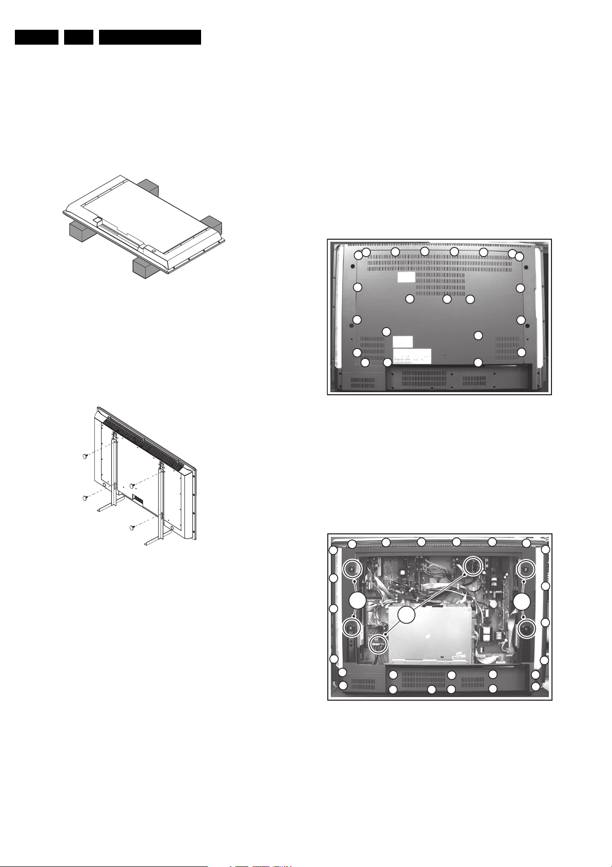
4.3 Assy/PWB Removal
4.3.1 Metal Back Plate
Caution: Disconnect the mains power cord before you remove
the metal back plate.
1. Place the TV set upside down on a table top, using the
foam bars (see part "Foam Bars").
Caution: do not put pressure on the display, but let the
monitor lean on the speakers or the Front cover.
2. Remove all T10 parker screws [1] from the top, left, and
right sides of the metal back plate.
3. Remove all T10 tapping screws [2] from the centre and
bottom of the metal back plate.
4. Lift the back plate from the TV. Make sure that wires and
flat foils are not damaged during the removal.
1
1
1
1
1
2
1
2
1
2
1
1
1
2
2
2
2
1
1
1
1
1
4.2.2 Aluminium Stands
E_06532_019.eps
170504
Figure 4-3 Aluminium stands (Mk1)
The new (Mk2) aluminium stands (order code 3122 785 90690)
can also be used to do measurements, alignments, and
duration tests. The stands can be (dis)mounted quick and easy
by means of sliding them in/out the "mushrooms".
Important: For (older) FTV sets without these "mushrooms", it
is obligatory to use the provided screws, otherwise it is possible
to damage the monitor inside!.
Figure 4-4 Metal back plate
4.3.2 Rear Cover
1. Disconnect all connectors [1] at both AmbiLight Inverters.
2. Remove all T10 parker screws [2] around the edges of the
rear cover.
3. Remove the four "mushrooms" [3] from the back plate.
4. Lift the rear cover from the TV.
2
2
2
2 2 2
2
3
2
1
2
2
2
2
2 2
2
2
F_15490_011.eps
3
2
2
F_15490_012.ep
2
230605
2
2
2
2
2
2
23060
Figure 4-5 Rear cover
4.3.3 LCD Supply Panel
1. Disconnect all cables from the LCD supply panel.
2. Remove all mounting screws from the LCD supply panel.
3. Take out the panel.
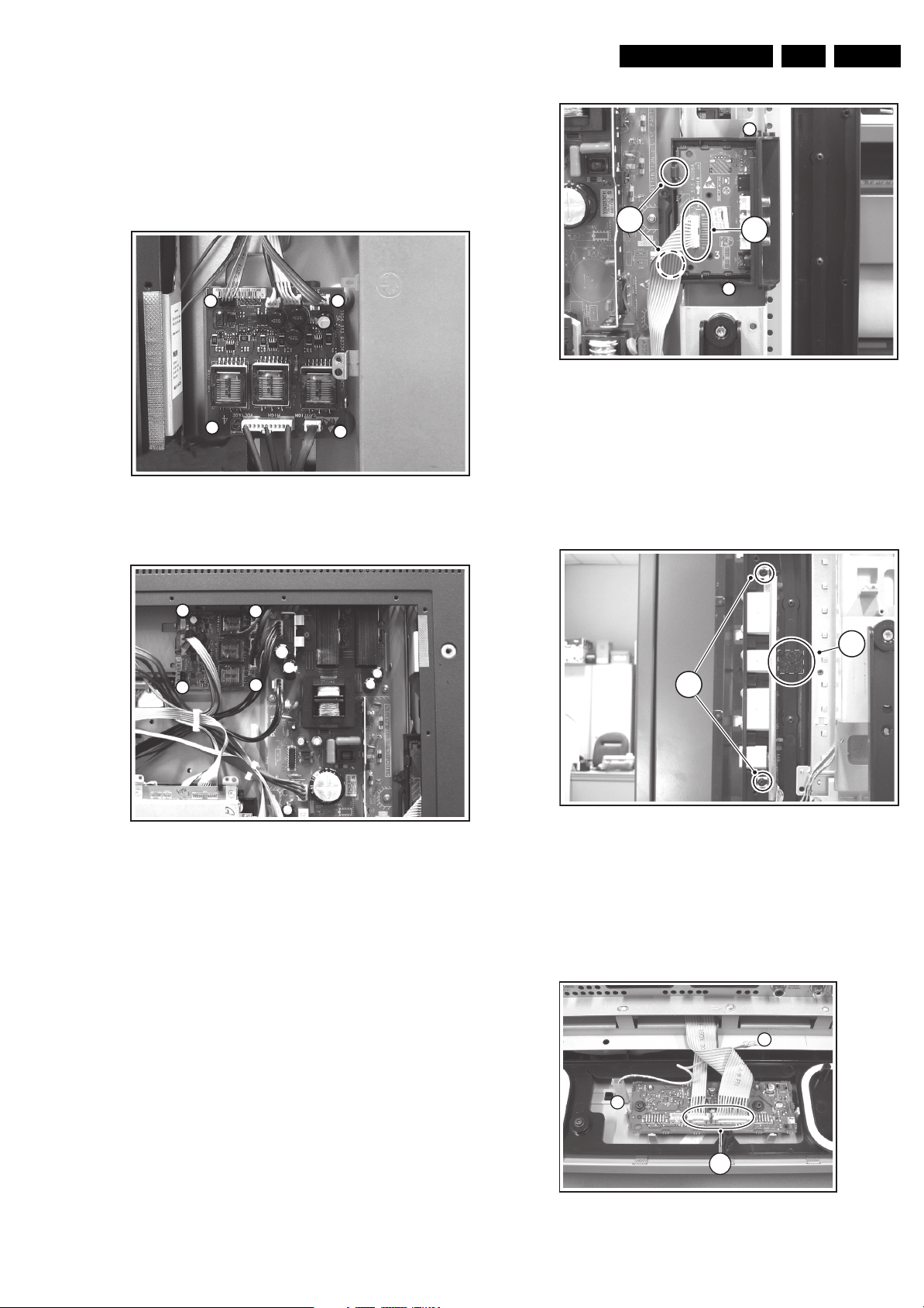
4.3.4 AmbiLight Inverter Panel
Mechanical Instructions
EN 9FTL2.4A AA 4.
These models are equipped with two AmbiLight Inverters
(however some early models can have only one inverter).
1. Disconnect all cables from the AmbiLight Inverter panel.
2. Remove all mounting screws [1] from the AmbiLight
Inverter panel.
3. Take out the panel.
1
1
1
1
F_15490_014.eps
230605
Figure 4-6 AmbiLight inverter (left lower side)
3
Figure 4-8 Side I/O panel
4.3.7 Control Panel
1. Remove the glued foam block [1].
2. Remove the assy mounting screws [2].
3. Take out the assy.
4. Release the clamps and take out the panel.
2
1
2
F_15490_024.eps
240605
1
1
1
1
Figure 4-7 AmbiLight inverter (right upper side)
4.3.5 Stand-by Supply/Audio Panel
1. Disconnect all cables from the Stand-by Supply/Audio
panel.
2. Remove all T10 mounting screws at the top of the Standby Supply/Audio panel.
3. Take out the panel (it hinges at the bottom side).
4.3.6 Side I/O Panel
F_15490_013.eps
230605
2
Figure 4-9 Local keyboard
4.3.8 LED Panel
1. Disconnect all cables [2] from the LED panel.
2. Remove the mounting screws from the LED panel.
3. Take out the panel.
1
F_15490_016.eps
240605
1
1. Disconnect the cable [1] from the Side I/O panel.
2. Remove the assy mounting screws [2].
3. Take out the assy.
4. Release the clamps [3] and take out the panel.
1
2
F_15490_025.eps
020805
Figure 4-10 LED panel & speaker grid grounding wire
EN 10 FTL2.4A AA4.
4.3.9 Speakers
1. After removal of the cover plate, you can access the
speakers.
2. Be sure that the foam that makes the unit airtight is not
damaged. Otherwise replace it.
Mechanical Instructions
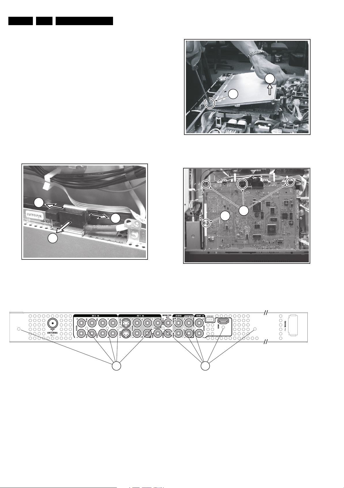
4.3.10 SSB
1. Remove the LVDS connector locking bracket [1][2].
2. Remove all shielding fixing screws.
3. Slide, and lift the shielding at the top [3]. The panel hinges
at the connector side. At the same time, use a screwdriver
to carefully prize the shielding at the bottom side [4], and
remove the shielding. The SSB is now accessible.
4. To remove the whole SSB, unscrew all fixing screws from
the connector plate [5]. See figure “Connector plate”.
5. Disconnect the LVDS cable, and all other cables.
6. Remove the mounting screw [8] from the SSB.
7. Bend the brackets [9] away (may require some force), lift
the SSB, and take it out.
1
1
2
For
PDP
4
Figure 4-12 SSB top shielding
9
8
3
F_15490_015.eps
230605
F_15490_017.eps
Figure 4-11 LVDS connector locking bracket
5 5
240605
Figure 4-14 Connector plate
Figure 4-13 SSB brackets
F_15490_027.eps
240605
F_15500_046.eps
020805
4.3.11 AmbiLight Lamp Unit
The AmbiLight lamp units are located in the TV’s rear cover.
1. Remove the cable clamps.
2. Remove all mounting AmbiLight screws.
3. Slide the AmbiLight unit to the side and take out the unit.
Mechanical Instructions
EN 11FTL2.4A AA 4.
6
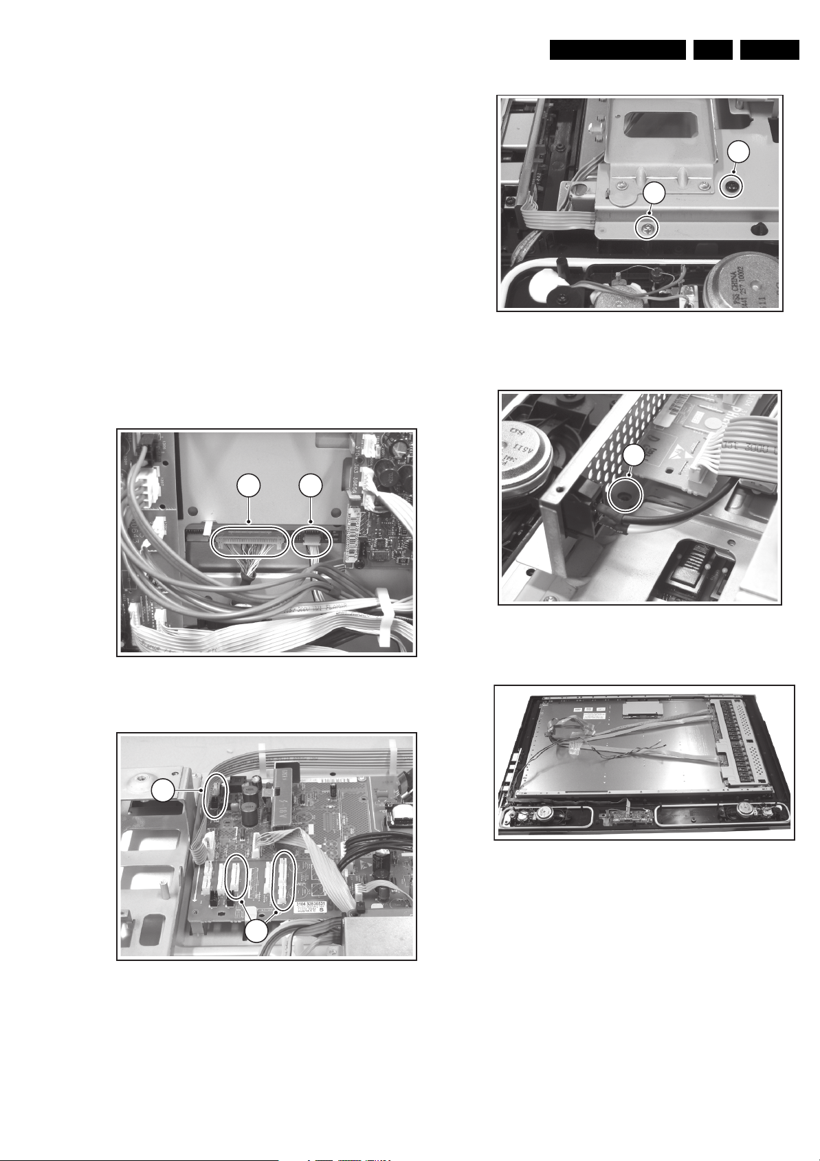
4.4 Display (Dis)Assembly
Important: Be sure to work in a dust free environment during
the following activities. In addition, the use of (fabric) hand
gloves is advised.
1. Important: Unplug the cables [1][2] at the LCD panel. Be
careful, as the LVDS connector [1] is very fragile!
2. Unplug the backlight and loudspeaker connectors [3][4].
3. Remove all T10 screws [5] from the mounting frame.
4. Remove all mounting LCD panel screws [6][7].
5. Lift the metal frame (together with all PWBs) from the LCD
panel. During lift, free the backlight and speaker cables.
6. After removal of the frame, you can lift the LCD display
from the set.
1 2
Fragile !
5
F_15490_019.eps
Figure 4-17 LCD panel disassembly (part 1)
3th SCART panel
(only for Europe)
7
240605
F_15490_018.eps
Figure 4-15 LCD panel connectors
3
4
F_15490_021.eps
Figure 4-16 Speaker and LCD backlight cables
240605
240605
Figure 4-18 LCD panel disassembly (part 2)
Figure 4-19 Bare LCD panel after frame removal
4.5 Set Re-assembly
To re-assemble the whole set, execute all processes in reverse
order.
Note: While re-assembling the TV, make sure that:
• All cables are placed and connected in their original
position (see figure “Chassis cable dressing” in the
beginning of this chapter and/or the “Wiring Diagram” in
chapter 6).
• LVDS connector (SSB) is secured with plastic clamp.
• The "grounding" wire between metal speaker grid and
frame is reconnected. See item [1] in figure “LED panel &
speaker grid grounding wire“.
F_15490_020.eps
290705
F_15490_022.eps
240605
EN 12 FTL2.4A AA5.
Service Modes, Error Codes, And Fault Finding
5. Service Modes, Error Codes, And Fault Finding
Index of this chapter:
5.1 Test Points
5.2 Service Modes
5.3 Problems And Solving Tips (Related To CSM)
5.4 Service Tools
5.5 Error Codes
5.6 The Blinking LED Procedure
5.7 Protections
5.8 Repair Tips
5.9 Software Downloading
5.1 Test Points
The chassis is equipped with test points printed on the circuit
board assemblies.
Perform measurements under the following conditions:
• Service Default Mode.
• Video: colour bar signal.
• Audio: 3 kHz left, 1 kHz right.
5.2 Service Modes
Service Default Mode (SDM) and Service Alignment Mode
(SAM) offer several features for the service technician, while
the Customer Service Mode (CSM) is used for communication
between a Philips Customer Care Centre (P3C) and a
customer.
There is also the option of using ComPair, a hardware interface
between a computer (see requirements below) and the TV
chassis. It offers the ability of structured troubleshooting, test
pattern generation, error code reading, software version readout, and software upgrading.
Minimum requirements: a Pentium processor, Windows 95/
98, and a CD-ROM drive (see also paragraph “ComPair”).
Remark: The silk screen printing is not correct for the SAM/
SDM indication. For the correct location of these pins, see
figure ”Service pads”.
5.2.1 Service Default Mode (SDM)
Purpose
• To create a pre-defined setting, to get the same
measurement results as given in this manual.
• To override SW protections.
• To start the blinking LED procedure.
– Smart modes.
– Auto store of personal presets.
– Auto user menu time-out.
How To Activate SDM
Use one of the following methods:
• Use the standard RC-transmitter and key in the code
“062596”, directly followed by the “MENU” button.
Note: It is possible that, together with the SDM, the main
menu will appear. To switch it off, push the “MENU” button
again.
SDM
SAM
SW UPGRADE
MODE
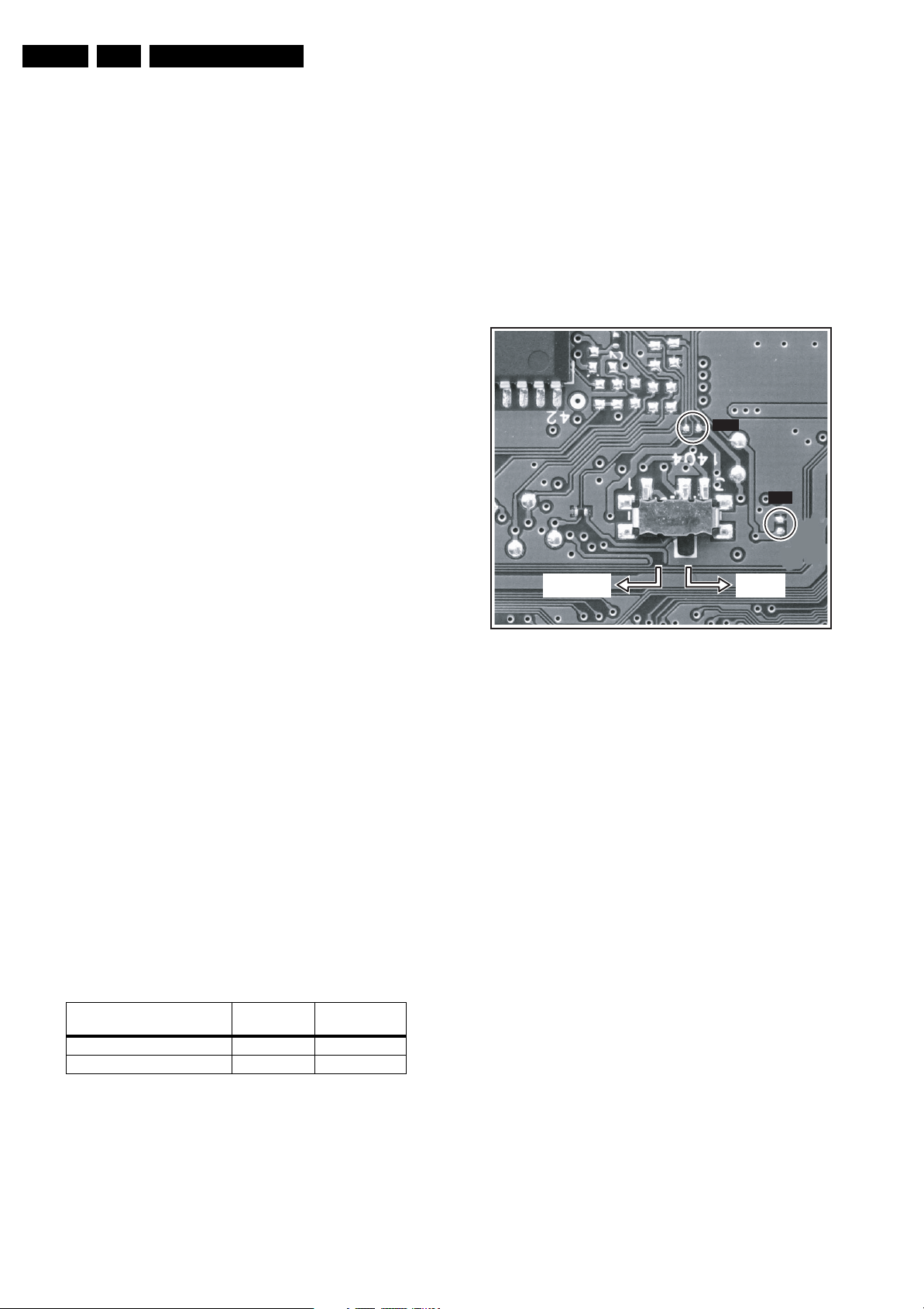
Figure 5-1 Service pads
• Short for a moment the two solder pads on the SSB, with
the indication “SDM” (see figure ”Service pads”). Activation
can be performed in all modes, except when the TV has a
problem with the main microprocessor.
Caution: If the SDM is activated via the pins, all the
software-controlled protections are de-activated.
• Use the DST-emulation feature of ComPair.
• Use the “DEFAULT” button on the Dealer Service Tool
(RC7150).
How To Navigate
When you press the “MENU” button on the RC transmitter, the
TV will toggle between the SDM and the normal user menu
(with the SDM mode still active in the background).
NORMAL
TV MODE
E_14620_151.eps
290704
Specifications
Table 5-1 SDM default settings
Default
Region Freq. (MHz)
Europe, AP-PAL/Multi 475.25 PAL B/G
NAFTA, AP-NTSC, LATAM 61.25 (ch. 3) NTSC M
• All picture settings at 50% (brightness, colour, contrast).
• All sound settings at 50%, except volume at 25%.
• All service-unfriendly modes (if present) are disabled, like:
– (Sleep) timer.
– Child/parental lock.
–Blue mute.
– Automatic volume limiter (AVL).
– Auto switch-off (when no video signal was received for
10 minutes).
– Skip/blank of non-favourite pre-sets.
system
How To Exit SDM
Use one of the following methods:
• Switch the TV to STANDBY via the RC-transmitter.
• Press the “EXIT” button on the DST.
• Via a standard customer RC-transmitter: key in “00”sequence.
5.2.2 Service Alignment Mode (SAM)
Purpose
• To perform (software) alignments.
• To change option settings.
• To easily identify the used software version.
• To view operation hours.
• To display (or clear) the error code buffer.
Specifications
• Operation hours counter.
• Software version.
Service Modes, Error Codes, And Fault Finding
EN 13FTL2.4A AA 5.
• Option settings.
• Error buffer reading and erasing.
• Software alignments.
How To Activate SAM
Use one of the following methods:
• Via a standard RC transmitter: key in the code “062596”
directly followed by the “OSD [i+]” button. After activating
SAM with this method a service warning will appear on the
screen, you can continue by pressing any digit key on the
RC.
• Short for a moment the two solder pads on the SSB with
the indication "SAM" (see figure ”Service pads”).
Depending on the software version, it is possible that a
service warning will appear. You can continue by pressing
any digit key on the RC.
• Use the DST-emulation feature of ComPair.
• Press the ALIGN button on the DST while the TV is in the
normal operation
After activating this mode, “SAM” will appear in the upper right
corner of the screen.
Contents Of SAM:
• Operation Hours. Displays the accumulated total of
operation hours (not the stand-by hours).
• Hardware Info.
– ROM Version. Displays the date of the software and
the software version of the ROM
Ex.: TX24EU_1.0_01234 = AAAABB_X.Y_NNNNN.
• AAAA= the chassis name.
• BB= the region: EU= Europe, AP= Asia Pacific
PAL/Multi, AN= Asia Pacific NTSC, US= USA, LT=
LATAM.
• X.Y= the software version, where X is the main
version number (different numbers are not
compatible with one another) and Y is the sub
version number (a higher number is always
compatible with a lower number).
• NNNNN= last five digits of 12nc code software.
– FBX Version. Displays the software version of the
FBX
– SW VERSION EPLD. Displays the software version of
the EPLD.
• Errors. (followed by maximal 10 errors). The most recent
error is displayed at the upper left (for an error explanation
see paragraph “Error Codes”).
• Defective Module. Here the module that generates the
error is displayed. If there are multiple errors in the buffer,
which are not all generated by a single module, there is
probably another defect. It will then display the message
“UNKNOWN” here.
• Reset Error Buffer. When you press the “OK” button, the
error buffer is reset.
• Alignments. This will activate the “ALIGNMENTS” submenu.
• Dealer Options. Extra features for the dealers.
• Service Options. Extra features for Service.
• Initialise NVM. The moment the processor recognises a
corrupted NVM, the “initialise NVM” line will be highlighted.
Now, you can do two things (dependent of the service
instructions at that moment):
– Save the content of the NVM via ComPair for
development analysis, before initialising. This will give
the Philips Service department an extra possibility for
diagnosis (e.g. when Development asks for this).
– Initialise the NVM (same as in the past, however now it
happens conscious).
Note: When you have a corrupted NVM, or you have replaced
the NVM, there is a high possibility that you will not have picture
any more because your display option is not correct. So, before
you can initialize your NVM via the SAM, you need to have a
picture and therefore you need the correct display option. This
code can be found on the option code sticker inside the set.
• Store. All options and alignments are stored when
pressing the “OK”-button
• Functional Test. All devices are tested via the “OK”
button. Eventual errors are displayed in the error buffer.
The error buffer is not erased, the content returns when this
test is terminated.
• Daily Menus. With the “OK” button, you can go to the
normal user menu. SAM is still active in the background.
With the “MENU” button, you return from the user menu to
SAM menu. This feature can be helpful to quickly change
some settings in the user menu.
• SW Maintenance.
• Upgrade. More info see paragraph Software
downloading.
• Events. Not useful for service purposes. In case of
specific software problems, the development
department can ask for this info.
• BDM Info. Broadcast Debug Menu info. The purpose
of this menu is to debug the broadcast, not the TV. The
menu gives an overview of what is received on the
current preset.
Following items are displayed:
P r e s e t n r : -- UTC: - - : - - : --
P r e s e t n a m e : ----- LTO: - - : - - : --
Time: - - : - - : --
C N I N V M : ---- Date: - - / - - / ----
C N I F 1 : ----
C N I F 2 : ---- Time TXT: - - : - - : --
C N I V P S : ---- Time 8/30 F1: - - : - - : --
M o r n i n g P r o g : --- Date 8/30 F1: - - / - - / ----
N a m e 8 / 3 0 F 1 : ----- LTO 8/30 F1: - - : - - : --
N a m e 8 / 3 0 F 2 : -----
N a m e T X T : ----- WSS G1: - - - -
S i g n a l S t r e n g t h :--- WSS G2: - - - -
WSS G3: - - -
E P G S e r v i c e : --- WSS G4: - - -
E_14620_050.eps
170504
Figure 5-2 Broadcast debug menu overview
Table 5-2 Broadcast debug menu explanation
Item Source Description
Presetnr Set Preset number of the current selected preset.
Presetname Set Preset name of the current selected preset.
CNI NVM Broadcaster CNI number stored in NVM for the current preset.
CNI F1 Broadcaster CNI number from transmitted Packet 8/30 Format
CNI F2 Broadcaster CNI number from transmitted Packet 8/30 Format
CNI VPS Broadcaster CNI number from transmitted VPS line.
Morning Prog Broadcaster "ARD" or "ZDF" according to dedicated bit in 8/30
Name 8/30 F1 Broadcaster Name extracted from status message of 8/30
Name 8/30 F2 Broadcaster Name extracted from status message of 8/30
Name TXT Broadcaster Name extracted from TXT header.
Signal Strength FBX Noise figure measured for selected preset.
EPG Service Set EPG Service stored in NVM for current preset
UTC Set UTC (Universal Time Code formerly known as
LTO Set LTO (Local Time Offset) used in the TV. Used by
Time Set Current time running in the TV. Was extracted at
Date Set Current date running in the TV. Was extracted at
Time TXT Broadcaster TXT header time from the selected preset.
Time 8/30 F1 Broadcaster UTC time from 8/30 Format 1.
Date 8/30 F1 Broadcaster Date from 8/30 Format 1.
LTO 8/30 F1 Broadcaster LTO from 8/30 Format 1.
WSS G1 Broadcaster WSS Group 1 (Aspect Ratio) bits 0 1 2 3
WSS G2 Broadcaster WSS Group 2 (Enhanced Services) bits 4 5 6 7
WSS G3 Broadcaster WSS Group 3 (Subtitles) bits 8 9 10
WSS G4 Broadcaster WSS Group 4 (Reserved) bits 11 12 13
1.
2.
Format 1.
Format 1.
Format 2.
displayed as "TXT", "MCP", "SCP", "OCP".
Greenwich Mean Time) used in the TV.
EPG for all NextView displays. (= Time TXT
header - Time 8/30 F1)
start-up, then maintained by software.
start-up, then maintained by software.

EN 14 FTL2.4A AA5.
Service Modes, Error Codes, And Fault Finding
How To Navigate
• In SAM, you can select the menu items with the “CURSOR
UP/DOWN” key on the RC-transmitter. The selected item
will be highlighted. When not all menu items fit on the
screen, move the “CURSOR UP/DOWN” key to display the
next/previous menu items.
• With the “CURSOR LEFT/RIGHT” keys, it is possible to:
– (De) activate the selected menu item.
– Change the value of the selected menu item.
– Activate the selected sub-menu.
How To Exit SAM
Use one of the following methods:
• Press the “MENU” button on the RC-transmitter, or
• Switch the TV to STANDBY via the RC-transmitter, or
• Press the “EXIT” button on the DST.
5.2.3 Customer Service Mode (CSM)
Purpose
When a customer is having problems with his TV-set, he can
call his dealer. The service technician can than ask the
customer to activate the CSM, in order to identify the status of
the TV. Now, the service technician can judge the severity of
the complaint. In many cases, he can advise the customer how
to solve the problem, or he can decide if it is necessary to visit
the customer.
The CSM is a read only mode; therefore, modifications in this
mode are not possible.
How To Activate CSM
Use the following method:
Key in the code “123654” via the standard RC transmitter.
Note: Activation of the CSM is only possible if there is no (user)
menu on the screen!
How To Navigate
By means of the “CURSOR-DOWN/UP” knob on the RCtransmitter, you can navigate through the menus.
Contents Of Csm
CUSTOMER SERVICE MENU 1
• Software Version (example: TX24EU_1.0_01234).
Displays the built-in software version. In case of field
problems related to software, software can be upgraded
(for more details, see paragraph Software downloading).
You will find details of the software versions in the chapter
“Software Survey” of the “Product Survey - Colour
Television” publication. This publication is generated four
times a year.
• Feature Box. The 12NC-number of the built-in Feature
Box software.
• Set Type. This information is very helpful for a help desk/
workshop as reference for further diagnosis. In this way, it
is not necessary for the customer to look at the rear of the
TV-set.
• Code 1. Gives the latest five errors of the error buffer. As
soon as the built-in diagnose software has detected an
error the buffer is adapted. The last occurred error is
displayed on the left most position. Each error code is
displayed as a 3-digit number. When less than 10 errors
occur, the rest of the buffer is empty (000). See also
paragraph Error Codes for a description.
• Code 2. Gives the first five errors of the error buffer. See
also paragraph Error Codes for a description.
• Volume. Gives the last status of the volume as set by the
customer. The value can vary from 0 (volume is minimum)
to 100 (volume is maximum). Volume values can be
changed via the volume key on the RC-transmitter.
• Brightness. Gives the last status of the brightness as set
by the customer. The value can vary from 0 (brightness is
minimum) to 100 (brightness is maximum). Brightness
values can be changed via the “CURSOR LEFT” and
“CURSOR RIGHT” keys on the RC-transmitter after
pressing the “MENU” button and selecting “PICTURE” and
“BRIGHTNESS”.
• Contrast. Gives the last status of the contrast as set by the
customer. The value can vary from 0 (contrast is minimum)
to 100 (contrast is maximum). Contrast values can be
changed via “CURSOR LEFT” and “CURSOR RIGHT”
keys on the RC-transmitter after pressing the “MENU”
button and selecting “PICTURE” and “CONTRAST”.
• Colour. Gives the last status of the colour saturation, as
set by the customer. The value can vary from 0 (colour is
minimum) to 100 (colour is maximum). Colour values can
be changed via “CURSOR LEFT” and “CURSOR RIGHT”
keys on the RC-transmitter after pressing the “MENU”
button and selecting “PICTURE” and “COLOUR”.
• Hue. Only relevant for NTSC-signals (e.g. some NTSCDVD-discs).
CUSTOMER SERVICE MENU 2
• Sharpness. Gives the sharpness value. The value can
vary from 0 (sharpness is minimum) to 7 (sharpness is
maximum). In case of bad antenna signals, a too high
value of the sharpness can result in a noisy picture.
Sharpness values can be changed via the “CURSOR
LEFT” and “CURSOR RIGHT” keys on the RC-transmitter
after pressing the “MENU” button and selecting “PICTURE”
and “SHARPNESS”.
• Headphone Volume. Gives the last status of the head
phone volume, as set by the customer. The value can vary
from 0 (volume is minimum) to 100 (volume is maximum).
Head phone volume values can be changed via the
“CURSOR LEFT” and “CURSOR RIGHT” keys on the RCtransmitter after pressing the “MENU” button and selecting
“SOUND” and “HEADPHONE VOLUME”.
• Dolby. Indicates whether the received transmitter
transmits Dolby sound (“ON”) or not (“OFF”). Attention: The
presence of Dolby can only be tested by the software on
the Dolby Signalling bit. If a Dolby transmission is received
without a Dolby Signalling bit, this indicator will show “OFF”
even though a Dolby transmission is received.
• Surround Mode. Indicates the by the customer selected
surround mode (or automatically chosen mode). Possible
values are “OFF”, “INCREDIBLE SURROUND” OR
“DOLBY VIRTUAL”. These settings can be influenced after
pressing the “MENU” button and selecting “SOUND” and
SURROUND MODE”. It can also have been selected
automatically by signalling bits (internal software).
• Tuner Frequency. Indicates the frequency the selected
transmitter is tuned to. The tuner frequency can be
changed via the “CURSOR LEFT” and “CURSOR RIGHT”
keys for fine tune after opening the installation menu and
selecting “INSTALL” and “MANUAL INSTALL”.
• Digital Option. Gives the selected digital mode,
“PROGRESSIVE SCAN”, “MOVIE PLUS” or “PIXEL
PLUS”. Change via “MENU”, “PICTURE”, “DIGITAL
OPTIONS”.
• Centre Trim. Not applicable for this set.
• TV System. Gives information about the video system of
the selected transmitter.
– BG: PAL BG signal received.
– DK: PAL DK signal received.
– I: PAL I signal received.
– L/La: SECAM L/La signals received.
– M: NTSC M signal received with video carrier on 38.9
MHz.
CUSTOMER SERVICE MENU 3
• Balance. Indicates the balance settings, between “-50”
and “+50”. Change via “MENU”, “SOUND”, and
“BALANCE”. Not applicable for Dolby Pro Logic sets.
• Centre Mode. Not applicable for this TV.

Service Modes, Error Codes, And Fault Finding
EN 15FTL2.4A AA 5.
• DNR. Gives the selected DNR setting (Dynamic Noise
Reduction), “OFF”, “MINIMUM”, “MEDIUM”, or
“MAXIMUM”. Change via “MENU”, “PICTURE”, “DNR”
• Noise Figure. Gives the noise ratio for the selected
transmitter. This value can vary from 0 (good signal) to 127
(average signal) and to 255 (bad signal). For some
software versions, the noise figure will only be valid when
“Active Control” is set to “medium” or “maximum”.
• Source. Indicates which source is used and the video/
audio signal quality of the selected source.
Example: Tuner, Video/NICAM) Source: “TUNER”,
“EXT1”, “EXT2”, “EXT3”, “EXT4”, “SIDE”, “AV1”, “AV2”,
“AV3” or “AV4”. Video signal quality: “VIDEO”, “S-VIDEO”,
“RGB 1FH”, “YPBPR 1FH 480P”, “YPBPR 1FH 576P”,
“YPBPR 1FH 1080I”, “YPBPR 2FH 480P”, “YPBPR 2FH
576P”, “YPBPR 2FH 1080I”, “RGB 2FH 480P”, “RGB 2FH
576P” or “RGB 2FH 1080I”. Audio signal quality:
“STEREO”, “SPDIF 1”, “SPDIF 2”, or “SPDIF”.
• Audio System. Gives information about the audio system
of the selected transmitter: “ANALOGUE MONO”,
“ANALOGUE STEREO”, “PCM 2/0”, “DD 1/0”, “DD 2/0
LtRt”, “DD 2/0 L0R0”, “DD 2/1”, “DD 2/2”, “DD 3/0”, “DD 3/
1”, “DD 3/2”, “DD 1+1”, “MPEG 1/0”, “MPEG 2/0”, “MPEG
2/0 LtRt”, “MPEG 2/1”, “MPEG 2/2”, “MPEG 3/0”, “MPEG
3/1”, “MPEG 3/2”, “MPEG 1+1” or “MPEG 2+2”.
• Tuned Bit. Gives information about the tuning method of
the stored pre-set. If a channel is found via “automatic
installation”, you will see the value “YES”. When you
change this (automatically found) frequency via “fine tune”
adjustment (installation menu - manual installation), the
displayed value will change to “NO”. Therefore, when you
see the value “NO” in this line, it is an indication that the
received channel is a non-standard signal (e.g. of a VCR).
• Surround Speakers. Not applicable in this set.
• On Timer. Indicates if the “On Timer” is set “ON” or “OFF”
and if the timer is “ON” also displays start time, start day
and program number. Change via “MENU”, “TV”,
“FEATURES”, and “ON TIMER”.
• Preset Lock. Indicates if the selected preset has a child
lock: “LOCKED” or “UNLOCKED”. Change via “MENU”,
“TV”, “FEATURES”, “CHILD LOCK”, and “CUSTOM
LOCK”.
CUSTOMER SERVICE MENU 4
• Child Lock. Indicates the last status of the general child
lock: “UNLOCK”, “LOCK”, or “CUSTOM LOCK”. Change
via “MENU”, “TV”, “FEATURES”, “CHILD LOCK”, and
“LOCK”.
• Age Lock. Indicates the last status of the EPG rating for
child lock: “OFF”, “4 YEARS”, “6 YEARS”, “8 YEARS”, “10
YEARS”, “12 YEARS”, “14 YEARS” or “16 YEARS”. This is
only displayed if child lock is set to “CUSTOM LOCK”
• Lock After. Indicates at what time the child lock is set:
“OFF” or e.g. “18:45” (lock time). This is only displayed if
child lock is set to “CUSTOM LOCK”
• Category Lock. Indicates the last status of the EPG theme
child lock: “MOVIES”, “NEWS”, “SHOWS”, “SPORTS”,
“CHILDREN”, “MUSIC”, “CULTURE”, or “SERIES”. This is
only displayed if child lock is set to “CUSTOM LOCK”. It is
possible that more than one value is shown.
• Program Category. Indicates the theme of the selected
transmitter: “MOVIES”, “NEWS”, “SHOWS”, “SPORTS”,
“CHILDREN”, “MUSIC”, “CULTURE”, or “SERIES”.
• TV Ratings Lock. Only applicable for US.
• Movie Ratings Lock. Only applicable for US.
• V-Chip TV Status. Only applicable for US.
CUSTOMER SERVICE MENU 5
• V-Chip Movie Status. Only applicable for US.
• Options 1. Gives the option codes of option group 1 as set
in SAM (Service Alignment Mode).
• Options 2. Gives the option codes of option group 2 as set
in SAM (Service Alignment Mode).
• AVL. Indicates the last status of AVL (Automatic Volume
Level): “ON” or “OFF”. Change via “MENU”, “TV”,
“SOUND”, “AVL”
• Delta Volume. Indicates the last status of the delta volume
for the selected preset as set by the customer: from “-12”
to “+12”. Change via “MENU”, “TV”, “SOUND”, “DELTA
VOLUME”.
• Front Spkr Dist. Not applicable for this TV.
• Front Spkr Dist. Not applicable for this TV.
How to exit CSM
Use one of the following methods:
• After you press a key on the RC-transmitter (with exception
of the “CHANNEL”, “VOLUME” and digit (0-9) keys), or
• After you switch the TV-set “OFF” with the mains switch.
Note: When you de-activate CSM, it is possible (depending on
the software version) that the size of the picture changes. This
can be solved by pushing “P+” and then “P-”.
5.3 Problems And Solving Tips (Related To CSM)
Note: Below described problems are all related to the TV
settings (visible in the CSM menu). The procedures to change
the value (or status) of the different settings are described
above. New value(s) are automatically stored.
5.3.1 Picture Problems
Snowy/Noisy Picture
1. Check in CSM line NOISE FIGURE. In case the value is
"127" or higher, and the value is also high on other
programs, check the aerial cable/aerial system. For some
software versions, the noise figure will only be valid when
“Active Control” is set to “medium” or “maximum”.
2. Check in CSM lines SHARPNESS and NOISE FIGURE. In
case the value of line SHARPNESS is "3" or "4" and the
value of line NOISE FIGURE is high ("127" or higher),
decrease the "Sharpness” value.
Picture Too Dark
1. Press “Menu”, “TV”, “Picture”, “Smart Picture”. In case the
picture improves, increase the “Brightness” or the
“Contrast” value. The new value(s) are automatically
stored (in “personal” pre-set) for all TV channels.
2. Check in CSM line BRIGHTNESS and CONTRAST. If the
value of these lines is low (< "10"), increase the
“Brightness” or the “Contrast” value via the user menu.
Picture Too Bright
1. Press “Menu”, “TV”, “Picture”, “Smart Picture”. In case the
picture improves, decrease the “Brightness” or the
“Contrast” value. The new value(s) are automatically
stored (in “personal” pre-set) for all TV channels.
2. Check in CSM lines BRIGHTNESS and CONTRAST. If the
value of these line is high (> 50), decrease the “Brightness”
value or increase the “Contrast” value via the user menu.
White Line Around Picture Elements And Text
1. Press “Menu”, “TV”, “Picture”, “Smart Picture”. In case the
picture improves, decrease the “Sharpness” value. The
new value is automatically stored (in “personal” pre-set) for
all TV channels.
2. Check in CSM line “Sharpness”. If the value is high,
decrease it. The new value is automatically stored for all
TV channels.
No Picture
Check in CSM line TUNED BIT. In case the value is “No”, install
the required program again. Open the installation menu and
perform manual installation.
EN 16 FTL2.4A AA5.
Service Modes, Error Codes, And Fault Finding
No Picture Or Unstable Picture
A scrambled or decoded signal is received.
Black And White Picture
Check in CSM line COLOUR. In case the value is low (< "10"),
increase the “Colour” value via the user menu. The new value
is automatically stored for all TV channels.
No Colours/colour Lines Around Pcture Elements Or Colours Not Correct Or Unstable Picture
1. Check in CSM line TV SYSTEM. If a “strange” system pops
up, something has gone wrong during installation. Reinstall the channel.
2. If in CSM line TV SYSTEM is “L”, then the installed system
for this pre-set is “France” (SECAM standard). if the
country requires a PAL standard, “West Europe” is
required. Install the required program again: open the
installation menu and perform manual installation. Select
system “West Europe”.
Menu Text Not Sharp Enough
1. Press “MENU”, “TV”, “PICTURE”, “SMART PICTURE”. In
case picture improves, decrease the contrast value. The
new value(s) are automatically stored for all TV channels.
2. Check line “Contrast”. If the value is high, decrease the
contrast value.
5.3.2 Sound Problems
buffer. Diagnosis is done on I
access the I
send and receive I
2
C/UART bus of the television. ComPair can
2
C/UART commands to the micro
2
C/UART level. ComPair can
controller of the television. In this way, it is possible for
ComPair to communicate (read and write) to devices on
2
the I
C/UART buses of the TV-set.
• Manually (by asking questions to you): Automatic
diagnosis is only possible if the micro controller of the
television is working correctly and only to a certain extend.
When this is not the case, ComPair will guide you through
the fault finding tree by asking you questions (e.g. Does the
screen give a picture? Click on the correct answer: YES /
NO) and showing you examples (e.g. Measure test-point I7
and click on the correct oscillogram you see on the
oscilloscope). You can answer by clicking on a link (e.g.
text or a waveform picture) that will bring you to the next
step in the fault finding process.
By a combination of automatic diagnostics and an interactive
question / answer procedure, ComPair will enable you to find
most problems in a fast and effective way.
How To Connect
This is described in the chassis fault finding database in
ComPair.
TO
UART SERVICE
CONNECTOR
TO
I2C SERVICE
CONNECTOR
NO Sound From Left and Right Speaker
Check line 6 “Volume”. The value is low. Increase the value of
“Volume”. The new value(s) are automatically stored (in
“personal” pre-set) for all TV channels.
5.4 Service Tools
5.4.1 ComPair
Introduction
ComPair (Computer Aided Repair) is a service tool for Philips
Consumer Electronics products. ComPair is a further
development on the European DST (service remote control),
which allows faster and more accurate diagnostics. ComPair
has three big advantages:
1. ComPair helps you to quickly get an understanding on how
to repair the chassis in a short time by guiding you
systematically through the repair procedures.
2. ComPair allows very detailed diagnostics (on I
is therefore capable of accurately indicating problem areas.
You do not have to know anything about I
yourself because ComPair takes care of this.
3. ComPair speeds up the repair time since it can
automatically communicate with the chassis (when the
microprocessor is working) and all repair information is
directly available. When ComPair is installed together with
the Force/SearchMan electronic manual of the defective
chassis, schematics and PWBs are only a mouse click
away.
Specifications
ComPair consists of a Windows based fault finding program
and an interface box between PC and the (defective) product.
The ComPair interface box is connected to the PC via a serial
(or RS-232) cable.
For this chassis, the ComPair interface box and the TV
communicate via a bi-directional service cable via the service
connector(s).
The ComPair fault finding program is able to determine the
problem of the defective television. ComPair can gather
diagnostic information in two ways:
• Automatic (by communication with the television): ComPair
can automatically read out the contents of the entire error
2
C level) and
2
C commands
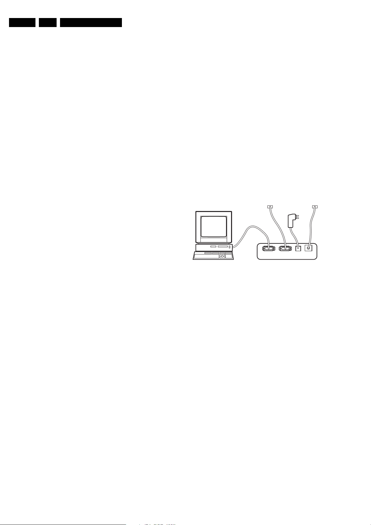
PC VCR I2CPower
9V DC
E_06532_021.eps
180804
Figure 5-3 ComPair interface connection
How To Order
• Starter kit ComPair32/SearchMan32 software and
ComPair interface (excl. transformer): 3122 785 90450.
• ComPair interface (excl. transformer): 4822 727 21631.
• Starter kit ComPair32 software (registration version): 3122
785 60040.
• Starter kit SearchMan32 software: 3122 785 60050.
• ComPair32 CD (update): 3122 785 60070 (year 2002),
3122 785 60110 (year 2003 onwards).
• SearchMan32 CD (update): 3122 785 60080 (year 2002),
3122 785 60120 (year 2003), 3122 785 60130 (year 2004).
• ComPair firmware upgrade IC: 3122 785 90510.
• Transformer (non-UK): 4822 727 21632.
• Transformer (UK): 4822 727 21633.
• ComPair interface cable: 3122 785 90004.
• ComPair interface extension cable: 3139 131 03791.
• ComPair UART interface cable: 3122 785 90630.
Note: If you encounter any problems, contact your local
support desk.
Stepwise Start-up
Under normal circumstances, a fault in the power supply, or an
error during start-up, will switch the television to protection
mode. ComPair can take over the initialisation of the television.
In this way, it is possible to distinguish which part of the startup routine (hence which circuitry) is causing the problem.
Take notice that the transition between two steps can take
some time, so give the set some time to reach a stable state.
During the transition time, the LED can blink strangely.
Service Modes, Error Codes, And Fault Finding
EN 17FTL2.4A AA 5.
Stepwise start- up explanation
This is realised via ComPair and is very helpful when a
protection is activated (see also chapter “Protections”). The
following diagram shows the start-up procedure of the set.
Every step of the stepwise start-up (also called trapped startup) in the diagram corresponds with the number of times the
LED blinks.
OUT
OTC gets supply voltage
OTC resets, Initialise IO pins
Reset Audio= HIGH
Read NVM identification
enable watchdog
Stand by bit = OFF
OFF
Time out:
30X200msec
Goto protection
400msec>t>200msec
Start time extraction
Start P50 recording
Start EPG loading
Standby bit = OFF
Ambient light ON
Trapped Startup 1
Trapped Startup 2
Mains cord IN
Stand by
Put Standby line LOW
CPU GO becomes HIGH
Set STBYEN,VCCON,PFCON= 1
Only FHP (opt 27)
Keep sound amplifiers muted
with sound enable = HIGH
+5V and +8V is switched ON
+8V and +5V get their nominal
level, detected by the OTC
Activate protection algorithms for +8V and
+5V and I²C (start I²C protection the
moment the component is initialised).
Read rest of NVM
information
Initialize HIP: IF, source selection, 2fh input, video processing
Switch ON the sync output: set_syncout_tristate= OFF
Initialize tuner
Initialize 3D Combfilter
or Initialize Columbus
Initialize PICNIC + screen info
Initialize rest of PIP/DW
module
Start TXT acquisition
and time extraction
Reset Audio = LOW
and Initialize MSP
5.4.2 LVDS Tool
Introduction
This service tool (also called “ComPair Assistant 1“) may help
you to identify, in case the TV does not show any picture,
whether the Small Signal Board (SSB) or the display of a Flat
TV is defective.
Furthermore it is possible to program EPLDs with this tool
(Byteblaster). Read the user manual for an explanation of this
feature.
Since 2004, the LVDS output connectors in our Flat TV models
are standardised (with some exceptions). With the two
delivered LVDS interface cables (31p and 20p) you can cover
most chassis (in special cases, an extra cable will be offered).
Tact switch
When operating, the tool will show a small (scaled) picture on
a VGA monitor. Due to a limited memory capacity, it is not
possible to increase the size when processing high-resolution
LVDS signals (>= 1280x768). Generally this tool is intended to
determine if the SSB is working or not. Thus to determine if
LVDS, RGB, and sync signals are okay.
How To Connect
Connections are explained in the user manual, which is
delivered with the tool.
Note: To use the LVDS tool, you must have ComPair release
2004-1 (or later) on your PC (engine version >= 2.2.05).
For every TV type number and screen size, one must choose
the proper settings via ComPair. The ComPair file will be
updated regularly with new introduced chassis information.
How To Order
• LVDS tool (incl. two LVDS cables: 31p and 20p):
3122 785 90671.
• Service Manual LVDS tool:
3122 785 00810.
Initialize EBILD
Screen type
Start up LCD
opt 3,4,5,6
Initialize PDP FHP
opt 2,8
Initialize PDP SDI
opt 0,1,7
Figure 5-4 Stepwise start-up part 1
Start up LCD
Trapped Startup 3
Start
Stand-by bit set ?
yes
Semi stand by
no
Ebild Power ON
Output Blanking OFF
LAMP ON
ON
Figure 5-5 Stepwise start-up part 2
Note: When the set is in stepwise mode and, due to stepping-
up, a protection is activated, the set will really go into protection
(blinking LED). The set will not leave the stepwise-mode
however. If state X is the state where the set went to protection,
stepwise start-up will return to state X-1. At state (X-1)
diagnostic measurements can be performed. Also, in the short
time the set is in state X but not yet in protection, you can also
do some measurements.
E_14620_048.eps
080805
LCD ON
Trapped Startup 4
E_14620_049.eps
170504
5.5 Error Codes
5.5.1 Introduction
The error code buffer contains all detected errors since the last
time the buffer was erased. The buffer is written from left to
right, new errors are logged at the left side, and all other errors
shift one position to the right.
When an error has occurred, the error is added to the list of
errors, provided the list is not full or the error is a protection
error.
When an error occurs and the error buffer is full, then the new
error is not added, and the error buffer stays intact (history is
maintained), except when the error is a protection error.
To prevent that an occasional error stays in the list forever, the
error is removed from the list after 50+ operation hours.
When multiple errors occur (errors occurred within a short time
span), there is a high probability that there is some relation
between them.
5.5.2 How To Read The Error Buffer
Use one of the following methods:
• On screen via the SAM (only if you have a picture).
Examples:
– 0 0 0 0 0: No errors detected
– 6 0 0 0 0: Error code 6 is the last and only detected
error
– 9 6 0 0 0: Error code 6 was first detected and error code
9 is the last detected error
• Via the blinking LED procedure (when you have no
picture). See next paragraph.
•Via ComPair.
EN 18 FTL2.4A AA5.
Service Modes, Error Codes, And Fault Finding
5.5.3 How To Clear The Error Buffer
Use one of the following methods:
• By activation of the “RESET ERROR BUFFER” command
in the SAM menu.
• With a normal RC, key in sequence “MUTE” followed by
“062599” and “OK”.
• When you transmit the commands “DIAGNOSE” - “99” “OK” with ComPair (or with a DST).
• If the content of the error buffer has not changed for 50+
hours, it resets automatically.
5.5.4 Error Codes
In case of non-intermittent faults, clear the error buffer before
you begin the repair. This to ensure that old error codes are no
Table 5-3 Error Code Overview
Error Device Description Def. item Def. Module indication Diagr.
1 M24Cxx NVM, spontaneous blinking error 1 7011 - B5a
3 SAA4978 PICNIC 7713 Feature Box B3a
4 Supply 5 V 5V protection - +5V Supply B5a
5 Supply 8 V 8V protection - +8V Supply B5a
6Slow I
2
C bus blocked Spontaneous blinking error 6 - Slow I2C Blocked 8 TDA932x HIP High-end Input Processor 7323 Chroma IF IO B2
13 UV1318/... Tuner protection 1T01 Tuner B13a
14 MSPxxxx ITT sound processor 7A02 Audio module B6a
2
18 Fast I
C bus blocked Spontaneous blinking error 18 - Fast I2C Blocked 21 M62320 I/O Expander 7P56 Video Dual Screen B15b
26 SAA4998 FEM (Falconic with Embedded Memory) 7760 +3V (FBX) Supply B3b
27 T6TX5 Eagle 1C 7720 +3V (FBX) Supply B3c
32 M29W400xx Flash Ram (EPG) 7012 EPG Memory B5a
35 T6TU5 Columbus 7752 Video Control B3d
55 DC/DC converter One of the voltages is not ok + protection error - MSB 76 Audio supply Audio supply protection - - 118 AD9883A AD converter 7L01 HD B19a
121 EPLD EPLD error 7V01 Video control B19d
Note: If error 3 or error 55 appears, sometimes error 16 is also logged. Error 16 is a non existing error.
longer present. Before clearing the buffer, write down the
content, as this history can give you significant information.
If possible, check the entire contents of the error buffer. In
some situations, an error code is only the result of another error
code and not the actual cause (e.g., a fault in the protection
detection circuitry can also lead to a protection).
There are various errors:
2
•I
C device errors.
2
•I
C bus errors.
• Protection errors.
• Errors not related to an I
2
C device, but of importance:
– FEM (Falconic with Embedded Memory) (Error 26):
at start-up, after initialisation of the PICNIC, the
presence of the FEM can be checked.
– Eagle (Error 27): at start-up, after initialisation of the
PICNIC, the presence of the Eagle can be checked.
Note:
• Error codes 1, 6, or 18 are protection codes and in this
case, supplies of some circuits will be switched “off”. Also,
in protection, the LED will blink the number of times
equivalent to the most recent error code.
Service Modes, Error Codes, And Fault Finding
EN 19FTL2.4A AA 5.
5.6 The Blinking LED Procedure
5.6.1 Introduction
Via this procedure, you can make the contents of the error
buffer visible via the front LED. This is especially useful for fault
finding, when there is no picture.
When the SDM is activated, the front LED will show (blink) the
contents of the error-buffer. Error-codes > 10 are shown as
follows:
– A long blink of 750 ms (which is an indication of the decimal
digit),
– A pause of 1.5 s,
– “n” short blinks (where “n” = 1 - 9),
– When all the error-codes are displayed, the sequence
finishes with a LED blink of 3 s,
– The sequence starts again.
Note: For error codes >100, the first two digits (hundred-andten) are considered as one digit (one long blink)
Example: Error 12 9 6 121 0.
After activation of the SDM, the front LED will show:
– 1 long blink of 750 ms (which is an indication of the decimal
digit) followed by a pause of 1.5 s,
– 2 short blinks followed by a pause of 3 s,
– 9 short blinks followed by a pause of 3 s,
– 6 short blinks followed by a pause of 3 s,
– 12 long blinks of 750 ms (which is an indication of “120”)
followed by a pause of 1.5 s,
– 1 short blink followed by a pause of 3 s,
– 1 long blink of 3 s to finish the sequence,
– The sequence starts again.
Note: If errors 1, 6, or 18 occur, the LED always gives the last
occurred error even if the TV is NOT in service mode.
protection mode is indicated by the blinking of the front LED at
a frequency of 3 Hz (or by a coded blinking in special cases).
The content of the error buffer can be read via the service menu
(SAM), the blinking LED procedure or via DST/ComPair.
To get a quick diagnosis, this chassis has three service-modes
implemented:
• The Customer Service Mode (CSM).
• The Service Default Mode (SDM). Start-up of the TV in a
predefined way.
• The Service Alignment Mode (SAM). In this mode, items
of the TV can be adjusted via a menu.
You can activate both SDM and SAM modes via the “service
pads” on the SSB (see figure “Service pads”), via an RCtransmitter (DST or standard RC), or via ComPair. It is not
possible to activate the SAM in “stand-by”; the TV has to be in
“normal operation” mode.
The “Protection Diagram” shows the structure of the protection
system. See diagram below.
TUNER
FAST I2C BUS BLOCKED
SLOW I2C BUS BLOCKED
EPLD
+
FBX
+
3D COMB
DC_PROT (from audio)
+8V_CON
+5V_CON
DC/DC
PROTECTION
IRQ-DIGITAL (98)
+8V SENSE (105)
+5V SENSE (106)
I2C
OTC
E_14650_032.eps
170604
5.6.2 How To Activate
Use one of the following methods:
• Activate the SDM (only via soldering pads marked “SDM”
on SSB, see figure “Service pads”). The blinking front LED
will show the entire contents of the error buffer (this works
in “normal operation” mode and in “protection” mode).
• Transmit the commands “MUTE” - “062500” - “OK” with a
normal RC. The complete error buffer is shown. Take
notice that it takes some seconds before the blinking LED
starts.
• Transmit the commands “MUTE” - “06250x” - “OK” with a
normal RC (where “x” is a number between 1 and 5). When
x= 1 the last detected error is shown, x= 2 the second last
error, etc.... Take notice that it takes some seconds before
the blinking LED starts.
• “DIAGNOSE X” with the DST (where “x” is a number
between 1 and 5). When x= 1 the last detected error is
shown, x= 2 the second last error, etc.... When x = 0 all
errors are shown.
5.7 Protections
5.7.1 Introduction
This chassis has only one microprocessor (OTC), which
remains active during Stand-by. This because power of the
microprocessor and the attached memory chip set is coming
from the 3V3 supply, which is derived from the 5V Stand-bycircuitry. Therefore, in both Power-on as in Stand-by mode, the
microprocessor is connected to this power supply.
If a fault situation is detected, an error code will be generated
and if necessary, the TV is put in protection mode. The
Figure 5-6 Protection diagram
There are several types of protections:
2
•I
C related protections.
• OTC related protections (via polling on I/O pins or via
algorithms).
• Hardware protection
All protections are explained below.
5.7.2 I
2
C Related Protections
In normal operation, some registers of the I
are refreshed every 200 ms. During this sequence, the I
buses and the I
2
An I
C protection will take place if the SDA and SCL lines are
2
C ICs are checked.
2
short-circuited to ground, or to each other. An I
occur, if the power supply of the IC is missing.
DC/DC protection: When a 3V3 supply is short-circuited, the
DC/DC converter switches “off” and goes in protection. The
FBX, EPLD IC, and 3D comb IC have no supply voltage and
give no acknowledge. In this case, the TV should go into
protection. An error code is written in the NVM: DC/DC error.
FBX protection: the FBX protection is not available any more.
It is replaced by the DC/DC protection.
5.7.3 OTC Related Protections
If a protection is detected at an OTC input, the OTC will start to
scan all protection inputs every 200 ms for 5 times. If the
protection on one of the inputs is still active after 1 s, the
microprocessor will put the TV in the protection mode. Before
the scanning is started, a so-called “ESD refresh” is carried out.
C controlled ICs
2
C error will also
2
C

EN 20 FTL2.4A AA5.
Service Modes, Error Codes, And Fault Finding
This is done, because the interrupt on one of the inputs is
possibly caused either by a flash or by ESD. As a flash or ESD
can influence IC settings, the HIP, MSP, 3D Comb and wireless
module (not used in this set) are initialised again, to ensure the
normal picture and sound conditions of the TV.
8 V and 5 V protections: The microprocessor senses the
presence of the 8 V and 5 V (via the “+5V_CON” and
“+8V_CON” lines). If one (or both) of these voltages is (are) not
present, an error code is stored in the error buffer of the NVM,
and the TV is put in the protection mode.
Audio Supply protection: The OTC senses if the audio
module is in protection via IRQ-DIGITAL (pin 98 of OTC). If this
is the case, the OTC puts the TV in protection.
5.7.4 Hardware Protection
Short-circuiting the 3V3 supply from the DC/DC converter will
shut down the DC/DC converter. The absence of the 3V3
supply line is also sensed via I
2
C (see description Audio Supply
protection above), this is useful if there is something wrong in
the detection circuit of the DC/DC converter.
Audio DC Protection: This protection occurs when there is a
DC voltage on the speakers. In that case, the Main Supply is
switched “off”. The Stand-by Supply is still working.
Repair tip: If there is an audio DC protection (DC voltage on
your speakers), you will probably see error 18 blink. To be sure
this is an audio DC protection, disconnect the cable between
the SSB and the audio PWB and also the cable between the
Main Supply and the Audio PWB. If the TV starts up, it is very
likely that there is DC on the speakers. Check, and replace if
necessary, the audio amplifiers.
Note: It is also possible that you have an Audio DC Protection
because of an interruption in one or both speakers (the DC
voltage that is still on the circuit can not disappear through the
speakers).
3. If you do not have two external power supplies, you can do
the following: Desolder coils 5U02, 5U03, and 5U04 (you
must desolder all three, otherwise the circuit could be
damaged), connect an external power supply of 3V3 at the
cathode of diode 6U06. Make sure to limit the current of this
external supply to approximately 1200 mA. If the supplied
current exceeds 1100 mA (approximately normal working
current) you can conclude that one of the devices supplied
by 3V3 is short-circuited.
4. Another possibility is to force the converter to start up by
short-circuiting (and keep short-circuited) resistor 3U25
(B12).
Caution: Be aware that this can damage the TV. Even if
you measure approximately 120 ohm over diode 6U06,
there can still be something wrong in the converter itself.
By short-circuiting resistor 3U25, the internal protection of
the converter is disabled.
5.8.2 Protections
Activating SDM via the “service pads” will overrule the
processor-controlled protections, but not the hardware
protections. This means, that the A/D-input protections (5 and
8 V) and the I
2
C “not-acknowledging” info of FBX + EPLD + 3D
Comb and of the tuner are overruled.
Caution: When doing this, the service technician must know
what he is doing, as it could lead to damaging the TV.
Note: It can sometimes take up to half a minute before the TV
goes to protection!
5.8 Repair Tips
5.8.1 3V3 Supply (DC/DC converter on the SSB)
As mentioned above, the DC/DC converter is switched “off”
when something goes wrong (detection of a missing 3V3
supply at one of the devices supplied by the 3V3). Because of
this, the TV goes to protection (I
is logged.
For further diagnoses, you need to overrule the I
put the TV in Service Default Mode by means of the solder
pads on the SSB (see figure “Service pads”).
The DC/DC converter is still not working because it is switched
“off” by the 3V3_FAULT line (schematic B12). Now you have
some possibilities:
1. First, measure the impedance over diode 6U06. In normal
conditions, you should measure approximately 120 ohm (if
possible, verify this with another set). If the impedance is
much too low, do not try to start up the converter as
mentioned below. Be aware that if FET 7U03 is shortcircuited, this will also influence your measurement.
2. Desolder coils 5U05 and 5U06, connect an external 3V3
supply at capacitor 2U23 (current limitation to 500 mA) and
a second external 3V3 supply at capacitor 2U31 (current
limitation to 800 mA). The normal working current of the
3V3_SIM line is approximately 400 mA and the normal
working current for the 3V3_DCDCFBX line is
approximately 700 mA. Therefore, if one of the currents
exceeds their nominal value you can determine in which
circuit the overload is situated. If the TV would start up and
you have normal picture, there is probably no overload but
a problem in the detection circuits.
2
C protection). Error code “55”
2
C protection:
5.8.3 Repair Tip Table
Table 5-4 Repair tips
Phenomenon Possible Cause Repair tip
“F” in the right corner of the screen and the set is not
reacting on the remote control. The local keyboard is
functioning.
No picture, LED blinking at 3 Hz. Set is in protection due to various causes.
No picture, LED blinking with code 6-6-6 or 18-18-18. No communication on slow I2C- or fast I2C-bus. As processor cannot communicate with one of the 2 buses, the Stand-by-LED
No picture, LED blinking with code 1-1-1. No communication on NVM-I2C bus to the uP. As the uP cannot communicate with the NVM I2C bus, it spontaneously starts
No RC-reception. Blue LED does not echo RCcommands.
Picture is not synchronised. The sync is derived in the HIP. Check crystals in the HIP circuit on bad contacts.
Picture is distorted. Check video-path in Service Default Mode. Investigate whether there is an error code present in the error buffer. In case
Picture with horizontal stripes. Pixel Plus processing is malfunctioning Check functionality on circuitry (B3a, B3b, B3c and B3d) of PICNIC, FEM,
No NextView (EPG). IC7012 defective or not powered. Check circuitry around IC7012 on diagram “B5a”.
No Teletext. IC7007 defective or not powered. Check circuitry around IC7007 on diagram “B5a”.
Problems caused by EPG (Electronic Program Guide).
The TV set "hangs".
NexTView EPG is not functioning only Teletext guide. EPG version 2C3 is switched “off” during
Various symptoms, due to missing local supply voltage. An interrupted fuse, NFR-resistor or connection. When no symptom or error code leads you to a specific circuitry, use the supply
No sound at the speakers but sound at monitor out. Possible problem with the class D amplifier Check circuitry around IC7700 on diagram “SA3” (LCD) or “C” (PDP).
No sound at the speakers but sound at monitor out. Sound enable from OTC is HIGH, speakers are
No sound at the speakers not at monitor out, but sound
at SCART 1 output.
No sound from any output (except headphone) Reset audio is high or MSP is not properly reset Check pin 16 of MSP (diagram “B6a”) and circuitry around MSP.
No sound from the tuner but sound from any other input. Problem with the delay line (PDP sets only) Check circuitry on diagram “B6d”.
Service Modes, Error Codes, And Fault Finding
TV is in factory mode. Press the “VOL-” button on the local keyboard for at least 3 seconds. Switch the
For error codes see error-code list.
uP circuitry or RC-receiver is defective. In case the TV does react on a local keyboard operation, you must check the
Problems with NexTView EPG broadcasts. To switch from EPG 2C3 to Teletext guide, press for 4 seconds, simultaneously
production.
muted
POR line is low, anti plop circuit mutes the sound Check pin 8 on connector 1739 on audio panel. Diagram “C” for PDP sets and
TV “off” and back “on”. The TV has now left Factory Mode and functions
normally again.
When pressing the “MENU” button on the local keyboard for at least 3 seconds,
you only leave Factory Mode temporarily. After switching “off” and back “on”, the
TV is in Factory Mode again.
You have no picture, so:
- Read the error buffer via ComPair (error buffer is accessible when set is in
protection, ComPair-file will guide you to this).
- Read the blinking LED information via standard remote command
<mute>06250x<ok>.
- Or you read the error code sequence via standard remote command
<mute>062500<ok>.
When you have found the error, check the circuitry related to the supply voltage
2
and I
spontaneously starts blinking 6-6-6-etc. or 18-18-18-etc...
If in the error buffer somewhere is an error 6 or 18, these will have the highest
priority starting the mentioned blinking.
Measure, dependent of the error on the I2C-bus, which device is loading the bus
(use I2C-overview).
blinking 1-1-1. Note: when there is no access to the NVM, a lot of picture setting
can go wrong.
RC-receiver circuitry (diagram “J”).
there is one, check the I
Measure and check signal path Tuner-HIP-FBX-EPLD.
EAGLE, COLUMBUS and/or field memories. Tip: the whole Pixel Plus chipset
can be diagnosed via ComPair.
the MENU button on the TV and digit 0 on the remote. The option settings for
NexTView type and FlashRAM will not change.
To switch from Teletext guide to EPG 2C3, press for 4 seconds, simultaneously
the MENU button on the TV and digit 1 on the remote. The option settings for
NexTView type and Flashram will not change.
lines overview (see supply lines overview), for a quick scan of all supply lines.
Check pin 95 of OTC on diagram “B5a”.
diagram “SA3” for LCD sets
C-communication or the circuitry that triggers the protection.
2
C-bus and/or supply lines (see overview supply lines).
EN 21FTL2.4A AA 5.
5.9 Software Downloading
In this chassis, you can upgrade the main software via
ComPair without removing the back cover of the TV (it is
possible that early production sets don’t have a hole in the back
plate, in this case you have to remove the back plate). The
switch, which is needed for the software downloading
procedure, can be reached through a gap in the back cover or
the SSB shielding. The switch can be operated with a toothpick
or something like that. Make sure that you do not damage the
PWB with sharp objects. You can find more information on how
this procedure works in the ComPair file. It is possible that not
all sets are equipped with the hardware, needed to make
software upgrading possible. To speed up the programming
process the firmware of the ComPair interface can be
upgraded. See paragraph “How To Order” for the order
number.

EN 22 FTL2.4A AA5.
Personal Notes:
Service Modes, Error Codes, And Fault Finding
E_06532_012.eps
131004
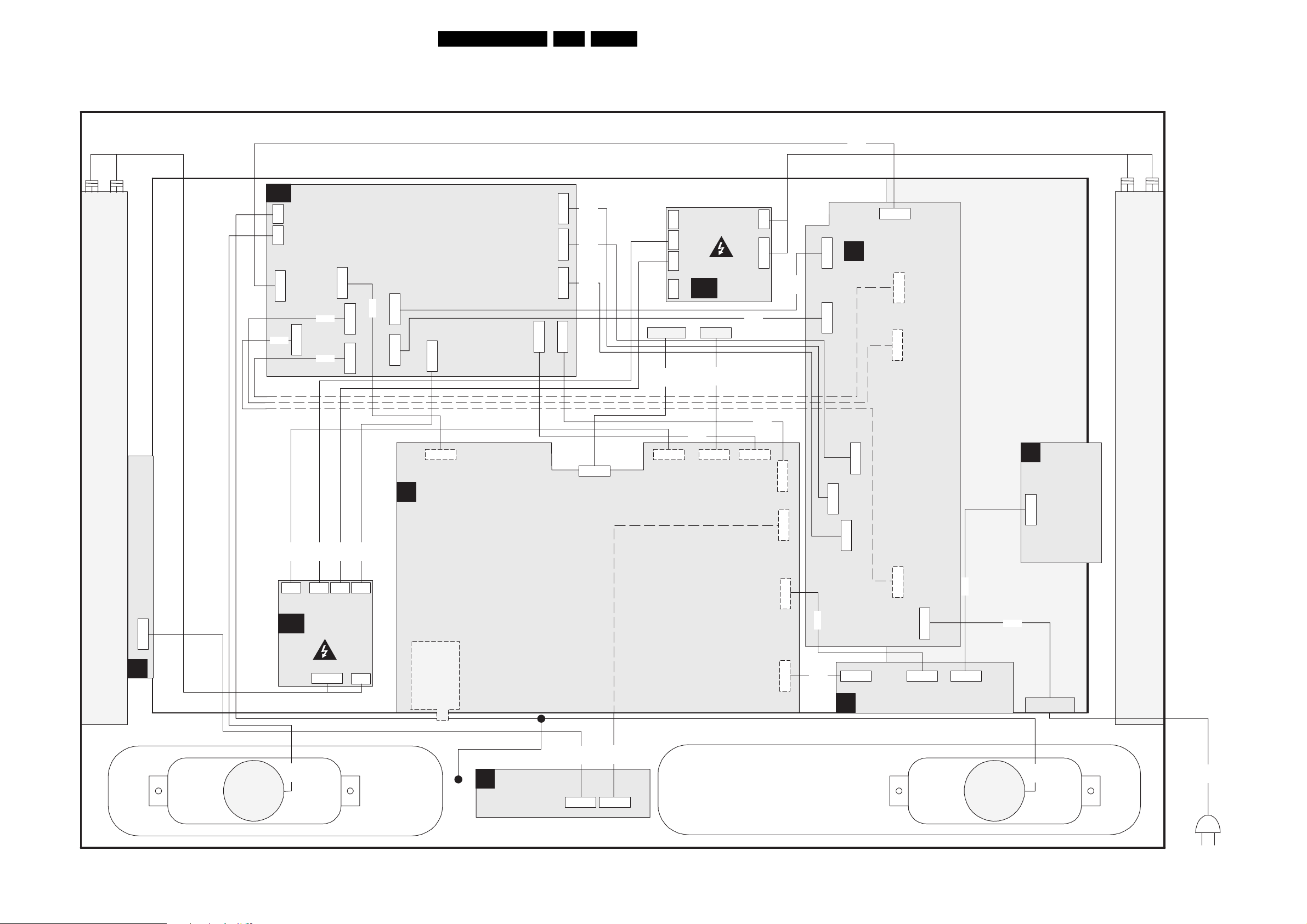
Block Diagrams, Testpoint Overviews, and Waveforms
6. Block Diagrams, Testpoint Overviews, and Waveforms
Wiring Diagram
Wiring 32"
EN 23FTL2.4A AA 6.
8302
SA
2P3
2P3
7P
8314
AMBIENT LIGHT LAMPS RIGHT
STANDBY SUPPLY / AUDIO AMPLIFIER
1736
1735
9P
8315
1314
8318
8548
1739
8508
10P
6P
1315
1318
8310
8352
1304
1309
4P
3P
B
4P
1M10
9P
1M52
SSB
1M02
10P
8349
1M46
11P
1306
1307
1305
1M03
2P3
4P
3P
10P
8506
8507
8505
31P
1G50
LVDS
31P
4P
1M51
8250
4P
4P
3P
4P
1M10
1M08
1M48
AL
1M49
8346
AMBIENT
LIGHT 1
7P
8317
7P
1M17
8509
8303
11P
1M46
1M12
1M11
3P
11P
10P
12P
8504
1M03
1M20
4P
3P
MF + SUPPLY
A
1304
1309
4P
1307
2P3
1606
3P
1305
7P
1MO2
6P
10P
CN3
CN4
INVERTERS
SIDE I/O
D
11P
1M36
T
LEF
MPS
LA
IGHT
ENT L
AMBI
TOP CONTROL
0345
E
6P
LS
RIGHT
4P
1M49
AL
8735
4P
3P
1M48
1M08
1M10
AMBIENT
LIGHT 2
1M11
1M12
11P
4P
3P
TUNER
LED PANEL
J
6P
0345
8345
12P
1M20
8220
1M36
1M07
11P
5P
8307
8337
5P
1M07
3th SCART
H
CN5
10P
2P3
1308
11P
1M37
(Only For EU)
11P
1M36
8336
LEFT
LS
8308
AC INLET
8736
F_15490_029.eps
090805
8192
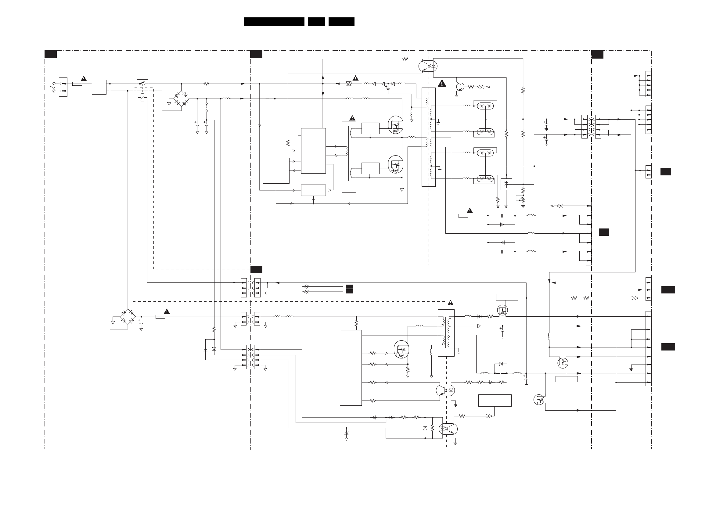
Block Diagrams, Testpoint Overviews, and Waveforms
Block Diagram Supply
SUPPLY 32"
MAINS FILTER + STANDBY PART A
A1
1400
F4A
5401
5402
MAINS
FILTER
1308
1
2
MAINS INPUT
6506
DF06M
EN 24FTL2.4A AA 6.
5009
5040
5104
3V MAX
1V MAX STBY
3108
3156
HOT COLD
1
4
2
3
5002
8
7
3
5
HOT COLD
5105
6156
3157
7002
TCET1102
9
10
11
12
13
14
15
16
COLD
HOT
5500
5
3
2
1
4
3
14
2
6
7
8
10
1
7501
TCET1102
2
3
7030
3031
5027
5028
5025
5026
1007
T5A
5110
3128
3158
7150
TCET1102
6044
STPS20L45CT
3
6045
3
6021
STPS20H100CT
3
6025
3
6504
6140
5103
3124
OVERVO LTAGE
PROTECTION
PROT-OVV
DC_PROT
2
2
2
2
7507
7506
7512
3509
6122
1
1
1
1
3030
2513
3022
2291
6291
6293
2293
STANDBY
2141
6107
3113
7010
TS2431AI
7511
5506
3057
3052
3025
VS Voltage
3026
Adj.
5293
5291
5292
2512
+12V
2021
+24V
2022
VSND_POS
GND_SND
VSND_NEG
+5V2-RELAY-IO2_PWM
+12V_A
5507
STANDBY
STANDBY: LOW = ON
HIGH = STBY
7531
DC_PROT
3534
VTUN
+11V
+12V
+8V6
7131
+5V2
+5V_SW
SA1
1304
44
33
22
11
1M02
7
6
5
4
3
2
1
3539
CONNECTIONS
1304
TO 1M02
SA3
AUDI O
+12V_A
+12V_+24V
POR
+5V_SW
1316
1317
1M10
1M03
1M46
1
2
3
4
5
1
2
3
4
5
1
2
9
5
2
8
11
9
4
3
6
7
5
TO
DISPLAY
TO
DISPLAY
TO 1M10
AL
AMBI LIGHT
TO 1M03
B21
CONNECTIONS
TO 1M46
B21
CONNECTIONS
F_15500_042.eps
290705
SUPPLY PART A
A2
1450
2
3
4
1
+
-
2503
HOT
COLD
1401
T1A
6807
GBJ6J
-
3810
+
9814
2816
2815
3101
6155
6154
RES
5004
RES
RES
25V_HOT
400V_HOT
1305
1306
11
22
1307
11
22
33
44
SA2
1305
11
22
33
1306
1307
7017
7018
SOFT
START
+
CURRENT
PROTECTION
STANDBY
+5V2
5504
3007
CONTROL
7505/7509/7560/
5505
7001
MC34067P
1
OSCC
CONTROL
7
ERROR
11
SOST
5
VREF
7004
7009
PROTECTION
BIAS SUPPLY
15
VCC
14
OA
12
OB
10
FI
OVER
VOLTAGE
Prot-OVV
PROT_AUDIOSUPPLY
3000
5007
5001
4
2
SA2
SA1
7100
7101
7105
CONTROL
6153
3101
6080
6077
5017
5008
STP15NK50ZFP
7007
HIGH
6
SIDE
DRIVE
7
STP15NK50ZFP
7008
LOW
10
SIDE
DRIVE
9
3104
3150
3127
3100
6150
6078
6151
3028
5010
2003
7005
7006
7102
3155
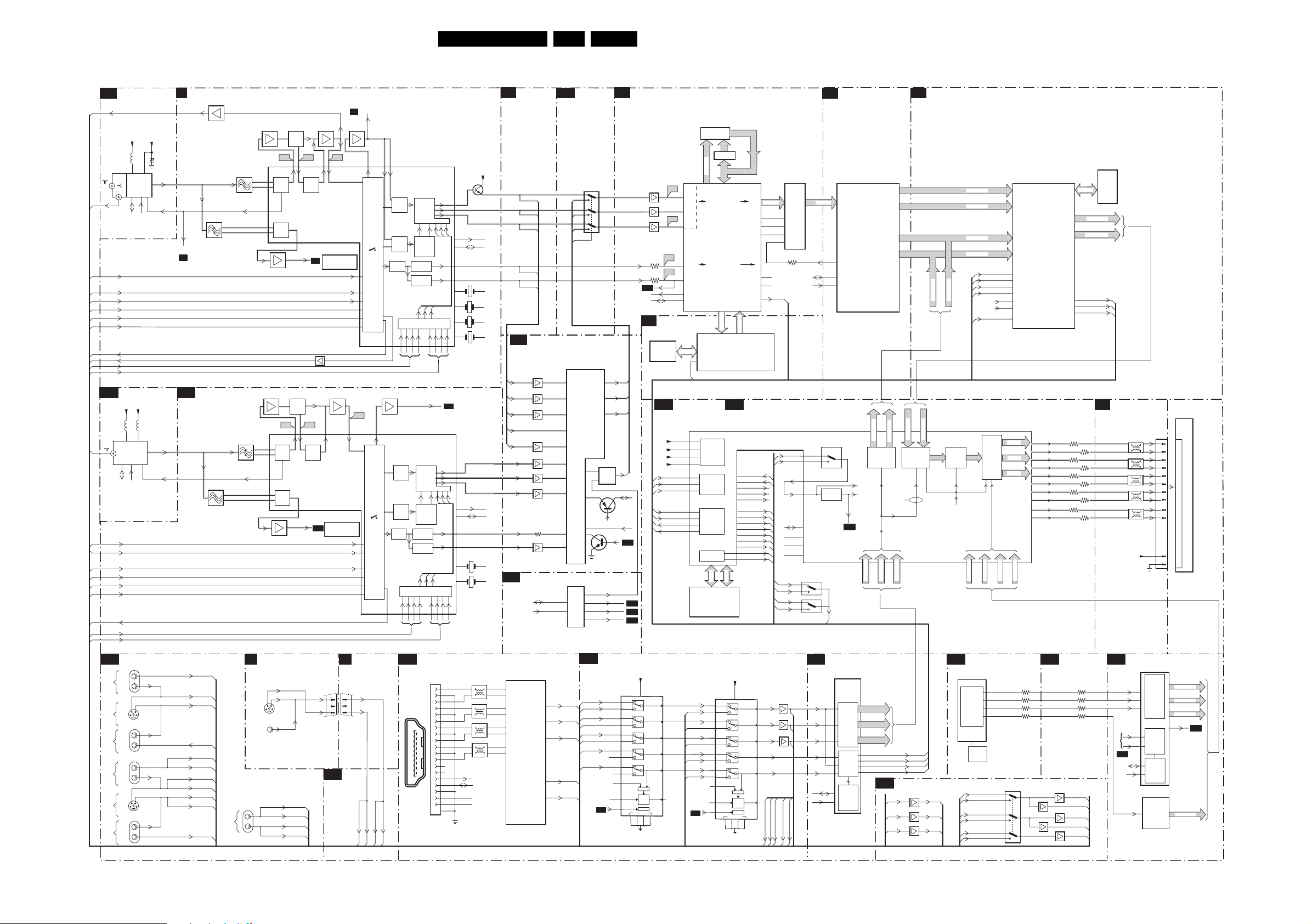
Block Diagrams, Testpoint Overviews, and Waveforms
Block Diagram Video
VIDEO
MAIN TUNER
B13A
B13B
1TO2
UV1318S
B14B
AV5
AV7
AV5
AV4
AV4
AV4
CVBS-TER-OUT
1TO1
UV1318ST
SUB TUNER
+5V
SUB TUNER
Pb
Y/C
CVBS
Pb/B
Pr/R
Y/C
Y/G
CVBS
S-SDA-PIP
Pr
Y
+5V
+33V
5T25
6TO8
9
7,3
11
MAIN TUNER
5
4
1
S-SDA-PIP
S-SCL-PIP
CVBS-SC1_AV1-IN
CVBS-AV3-IN
Y-CVBS-SC2_AV2-IN
C-SC2_SVHS-IN
Y-CVBS-FRONT-IN
C-FRONT-IN
PIP-OUT
CVBS-SC2-MON-OUT
R/G/B-SC1-Y/U/V-IN
SC2-FBL-IN
SC2-R_C-IN_AV2
SC2-G-IN
SC2-B-IN_C-OUT
+33V
5T02
5T04
7,3
9
11
15
4
S-SCL-PIP
IN-CVBS-SC1_AV1-SUB
AV3-CVBS-IN
IN-Y-CVBS-SC2_AV2
SC2-R_C-IN
Y-CVBS-PIPDW-OUT
C-PIPDW-OUT
PIP-OUT1
SUB-Y/U/V
SC2-FBL-IN
SC2-R_C-IN_AV2
SC2-G-IN
SC2-B-IN_C-OUT
1I01-2
34
1I10-A
21
1I01-3
1I04-2
910
1I10-B
87
1I04-3
AGC
AGC2
N.C.
B13b
B14b
B15a
B14b
B14b
B14a
B14a
N.C.
B14b
B14c
B14g
B13a
N.C.
B2
B14b
B14b
B14a
B14a
N.C.
B14c
B14g
IF, I/O VIDEOPROCESSING
B2
MONITOR
B5A
B15A
CVBS-SC2_MON-OUT
AV4-Y-G_AV2-Y-CVBS
IF-TER
AGC
PIP HIP
IF-TER2
AV5-PB
AV5-PR_AV7-C
AV5-Y_AV7-Y
AV4-PB-B
AV4-PR-R_AV2-C
CVBS-SC1_AV1-IN
SAW FILTER
AUDIO
1409
SAW FILTER
AUDIO
1P04-A
AV6- B
AV6- R
AV6- G
7402
B14c,g
B14c,g
B14c,g
B2
B14g
B14c
B14g
B14c
B14c
B14g
B2
(FOR AP)
(FOR AP)
(FOR AP)
AV1
SAW FILTER
VIDEO
1410
1408 (FOR AP)
TUNER AGC
SAW FILTER
VIDEO
1P05-A
1P06-A (FOR AP)
TUNER AGC
1I02
H
V
VIF1
VIF2
SIF2
SIF1
(FOR AP)
(FOR AP)
D
SVHS
7411
2
3
62
64
63
SOUND-OUTPUT
7P05
VIF1
VIF2
62
64
SIF2
63
SIF1
MONO-HIP-OUT
SIDE I/O
251
1002
CVBS
1406
1407 (FOR AP)
EF
SOUND
FILTER
I6
7323
TDA9321H
10 12 13 14
PLL
DEM
QSS
MIXER
QSS-AM
AM
DEMO
5
QSS-AM
7410
1P08
1P09 (FOR AP)
EF
SOUND
FILTER
I6
7P09
TDA9321H
10 12 13 14
2
PLL
3
DEM
QSS
MIXER
AM
DEMO
PIP-AM
7P07-2
C
Y
34
1001
AV6- H
AV4- H
AV4- V
AV6- V
(AP)
(AP)
QSS-AM
5
(US)
V1
GROUP
DELAY
COR.
V1
GROUP
DELAY
COR.
B6A
(US)
B14A
C
B14g
B14g
B14g
B14g
7322
EF
HIP
SEE
BLOCK DIAGRAM
AUDIO
7415
7P06
HIP
SEE
BLOCK DIAGRAM
AUDIO
1M36
24Y
3
B14A
V2
EF
B21
1M36
I/O 1
2
3
4
B5A
OTC
7320
CONNECT
CVBS-TXT
EF
12
26 29
VIDEO
SWITCH
+
CONTROL
16
18
20
21
23
24
V2
26
VIDEO
SWITCH
+
CONTROL
16
18
20
21
23
24
FRONT-Y-CVBS-IN
FRONT-C-IN
C-PIPDW-OUT
C-FRONT-IN
Y-CVBS-PIPDW-OUT
B2
B15a
B15a
28
CY
Y
PROC.
C
PROC.
SYNC
SEPAR.
32
32 34
7P08
EF
Y
C
SYNC
SEPAR.
32
Y-CVBS-FRONT-IN
B2
Y
C
R
G B
SCART1
36 37 38 39
Y
PROC.
C
PROC.
R
G B
SCART1
36 37 38 39
B14F
HDMI
CONNECTOR
Y
Y/U/V
U
SWITCH
V
UU
VY V
DECODER
PAL
NTSC
SECAM
H-SYNC
PROC.
V-SY NC
PROC.
UY
V
RGB/YUV
MATRIX
R G B
41 42 43 40
PIP-CVBS-MON
Y
Y/U/V
U
SWITCH
V
VY V
UU
DECODER
PAL
NTSC
SECAM
H-SYNC
PROC.
V-SY NC
PROC.
UY
V
RGB/YUV
MATRIX
R G B
41 42 43 40
1D01
1
2
3
4
5
6
7
1
8
9
10
11
12
13
14
18 2
15
19
16
17
18
19
20
+8VP
7414
49
50
51
SCL-F
46
SDA-F
47
60
61
1305
54
4.43MHz
1306
PAL N
55
3.58MHz
1307
PAL M
56
3.57GHz
1308
NTSC M
57
3.58MHz
SCART2
B15B
Y-HIP-OUT
49
U-HIP-OUT
50
51
V-HIP-OUT
SCL-S
46
SDA-S
47
VS-HIP-OUT
61
HS-HIP-OUT
60
1P00
54
4.43MHz
1P03
57
3.57MHz
SCART2
(NO PIP FOR STEP B SETS)
1I59
1I56
1I57
1I53
RX-DDC-SCL
RX-DDC-SDA
IN-5V
RX-HOTPLUG
Y50
U50
V50
HA50
VA50
AUDI O
B6A
DEMODULATOR
B15C
IN-Y50
IN-U50
IN-V50
VA50-PIP
HA50-PIP
B15B
7I18
SII9993CT
97
RX2+
RX2-
96
RX1+
92
RX1-
91
RX0+
87
86
RX0-
RXC+
84
RXC-
83
PANNELLINK
RECEIVER
IN-Y50
IN-U50
IN-V50
HA50-PIP
VA50-PIP
PIP MUPPET
7PA7
7PA8
7PA9
7PB2
7PB6
7PA0
7PA1
3PB8
7PA2
PIP SWITCH
SPDIF
HDMI
HA
SDA-S
SCL-S
7
IOR
IOG
12
15
IOB
34
33
PIP SWITCH
B15B
7P54
BA7609F
8
9
1
16
14
11
MUPPET-BLK
7PA6
SAB9081H
98 8
2
MUPPET
DOUBLE
100
WINDOW
PROC.
70
94
83
79
81
72
87
7P56
M62320
I/O
3
EXP
2
B14G
R-DV1
B14F
G-DVI
B14F
B-DVI
B14F
V-DVI
B14G
H-DVI
B14G
EN 25FTL2.4A AA 6.
6
3
5
7PB1
168
2
74
73
75
7PB5
9
SWITCH-MAIN
10
PIP_RESET
11
SWITCH-SUB
12
AV6- R
AV5-PR_AV7-C
AV6- G
AV5-Y_AV7-Y
AV6- B
AV5-PB
AV6- V
AV6- H
SWITCH-MAIN
B15B
GATE
OR
7PA5
FBLK
12
10
HA
B3A
Y-PIP+MAIN-OUT
U-PIP+MAIN-OUT
V-PIP+MAIN-OUT
HA50
VA50
B15b
DY
B15b
DU
B15b
DV
B15b
4
MUPPET_BLK
SDA-S
SCL-S
PIP-RESET
B15B
B14C
B15C
B14C
7I71
BA7657F
R1-IN
1
R2-IN
7
G1-IN
3
G2-IN
9
B1-IN
5
B2-IN
11
VD1-IN
12
VD2-IN
13
24
HD1-IN
HD2-IN
23
HD-S-SIG-DET
2
C-V-IN
18
CTL
16
468
PICNIC
+5VIO
20
VCC
1
2
1
2
1
2
1
2
1
2
SYNC
SEPA
LOGIC
GROUND
7775
7776
7777
3727
3728
B19d
B3D
7753
MSN56V16160F-7TS
SDRAM
B19B
B19a
B19a
B19a
B3a
B3a
B3a
B3a
R-OUT
G-OUT
B-OUT
VD-OUT
HD-OUT
DET
C-S-OUT
10
F162
F164
F165
F166
VA
SCL-F
SDA-F
COLUMBUS
EPLD CONTROL
+2V5-IO
+3V3-IO
+1V5-INT
+1V5-PLL
H-2FH-AD-OUT
V-2FH-AD-OUT
SYNCDET
VA
Href-EXT
HD-E
VD-E
21
B14F
19
B14F
15
B14F
14
B14F
22
B14F
17
7711
M27C512
7713
SAA4978H
23
3x
ADC
25
26
28
29
4
5
COL_SD
7V01
EP1C12Q240C0
7V03
MSM56V16160F
R-DV1
G-DVI
B-DVI
V-DVI
HDVI
SEL_IN_1_B
7752-1
T6TU5XB
Href-EXT
B3a
B14D
DEFLECTION
512KX16X2
64K
PROM
LATCH
AD(0-7)
DIGITAL
SIGNAL PROCESSING
PICNIC
SYNC PROCESSING
BUS A
UVA / YA
COLUMBUS
SUPPLY
STANDARD
SYNC
CONTROL
INPUT
CONTROL
SD-A
DRAM
7I55
BA7657F
R1-IN
1
R2-IN
7
G1-IN
3
G2-IN
9
B1-IN
5
B2-IN
11
VD1-IN
12
VD2-IN
13
HD1-IN
24
HD2-IN
23
HD-S-SIG-DET
2
C-V-IN
18
CTL
16
468
74HC573
BUS B
I/O
B19D
SD-DQ
+5VIO
20
VCC
1
2
1
2
1
2
1
2
1
2
SYNC
SEPA
LOGIC
GROUND
7712
UVB / YB
VD-OTC
HD3-OTC
PWR-OK-PDP
LCD-PWR-ON
LAMP-ON
CLK32E
Vref
Href
RSTR
REF
FALREF
REFIN
SWITCH-1FH
SWITCH-2FH
DET
10
BUS C
EPLD I/O
R-OUT
G-OUT
B-OUT
VD-OUT
HD-OUT
C-S-OUT
DA (0-15)
CLI6
WEC
RSTW
CLK32FM1
1
2
30
B19a
B3c
B19b
B19d
B19d
B19d
R-VGA
21
G-VGA
19
B-VGA
15
VS-2FH
14
HS-2FH
22
abcab
17
SC2-R_C-IN_AV2
B2,B15a
SN-DA
SN-CL
Href-EXT
B3a
B3a
B19d
B3c
B3c
B3c
B3c
B3c
B19b
B19b
CLK32P_EPLD
SWITCH-2FH
SWITCH-2FH
7I56
7I57
7I58
SC2-G-IN
SC2-B-IN_C-OUT
B2,B15a
B2,B15a
7714
MS81V04160A
FIELD
MEMORY
FM1
3724
CLK32
B3c,d,B19d
CLK-2FH
CLK-64
CLK-VID
SDA-F3
SCL-F3
SN-CL
SN-DA
CLK32E
a
b
c
Y-CVBS-SC2_AV2-IN
C-SC2_SVHS-IN
B2
B2
SNDA
SNCL
7E03
7E04
B19A
V-2FH
Y-2 F H
U-2FH
V-2FH
H-2FH
MF (1-17)
SDA-F3
SCL-F3
B3B
CLK32I
B3c
HDI A/D CONVERTEROTCI/O 7I/O 6: DIGITAL INPUT
1:2
48
54
43
31
49
30
FALCONIC
7760
SAA4998H
FALCONIC
EMBEDDED
MEMORY
83
34
41
CLKP
CLK-OSD
B19C
7L01
AD9883AKST
2-9
70-77
A/D
COVERTER
12-19
66
SYNC
64
PROC.
+
65
CLOCK
67
GENERATOR
SERIAL
B15a
REGISTER
+
POWER
MAN.
UVF (0-7)
UV
CONVERTION
U-AD (0-7)
H-2FH-AD-OUT
V-2FH-AD-OUT
SYNCDET
CLK-2FH
B14C
B14g
B14g
B14g
YF (0-7)
UV-AD (0-7)
Y-2 F H
U-2FH
V-2FH
B3C
Y-OUT (0-9)
UV DEMUX
CONTRAST
SATURATION
BRIGHTNESS
PATH
FOR
3FH
ONLY
EPLD
Y-AD (0-7)
I/O 3: SWITCH
7I29
7I31
7I27
EAGLE
U-VOUT (0-9)
B19d
B19d
B19d
B19b
G-SC1_Y-IN
B-SC1_U-IN
R-SC1_V-IN
UVF (0-7)
B2
B2
B2
YF (0-7)
YUV
to
RGB
CLKP
B5A
B14b
B14b
B14b
B14b
B14b
B14b
7001
SAA5801H
YG (0-7)
UVG (0-7)
YF (0-7)
UVF (0-7)
CLK32IN
163
FALREF
B19b
B19d
B19d
B19d
B19d
R-OSD (0-5)
REFIN
VAP_ E
SN-DA
SN-CL
HREF_EXT_E
OSD
INSERTION
G-OSD (0-5)
46
47
34
24
35
R (0-7)
G (0-7)
B (0-7)
B-OSD (0-5)
OTC
OTC
77 R-TXT 2FHR-GFX
78 G-TXT 2FHG-GFX
DIPLAY
INTERFACE
79 B-TXT 2FHB-GFX
80 FB-TXT 2FHFB-GFX
SEE ALSO
BLOCK
DIAGRAM
CONTROL
7I33
AV4-PR-R_AV2-C
AV5-PR_AV7-C
AV4-Y-G_AV2-Y-CVBS
AV5-Y_AV7-Y
AV4-PB-B
AV5-PB
3
5
1
2
13
12
74HC4053
7720
T6TX5AF
EAGLE
R7
R5
G6
G7
G5
B0
B5
PAR IT Y
B1
CLK-OUT
BL-OSD (0-4)
B3A
3064-1 3858
3064-2 3859
3064-3 3860
3064-4 3861
7I48-1
7I48-2
7I26
7I28
IN-Y-CVBS-SC2_AV2
7I30
4
15
14
118
26
27
3V25
3V27
4V29
3V31
3V33
SUB-V
SC2-R_C-IN
SUB-Y
SUB-U
EAG_SD
3V26
3V28
3V30
3V32
3V24
7719
MSM56V16160F
Y-OUT (0-9)
U-VOUT (0-9)
CLK64
HD-E
VD-E
B20
B15a
B15a
B15a
B15a
B15a
512KX16X2
DRAM
B19b
B3a
B3a
SCREEN
INTERFACE
5Z01
TXLCD0-
TXLCD0+
5Z02
TXLCD1-
TXLCD1+
5Z03
TXLCD2-
TXLCD2+
5Z05
TXLCD3-
TXLCD3+
5Z04
TXCLKLCD-
TXCLKLCD+
1,2,3,4
VDISP
11,14,17,20,23,26,27,28,29,32,33
EPLD OSDPICNICCONNECTIONS
B19C
7E23
AD9883AKST
R-OSD
G-OSD
B-OSD
HD3-OTC
VD-OTC
GENERATOR
B3A
SDA-F3
SCL-F3
7E24
AD9283BRS-80
BL-OSD
18
17
16
A/D
COVERTER
SYNC
PROC.
+
CLOCK
SERIAL
REGISTER
+
POWER
MAN.
8-BIT
ADC
1G50
15
14
13
10
9
12
11
DISPLAY
R-OSD (0-5)
G-OSD (0-5)
B-OSD (0-5)
CLK-OSD
B19D
BL-OSD (0-5)
F_15500_043.eps
290705
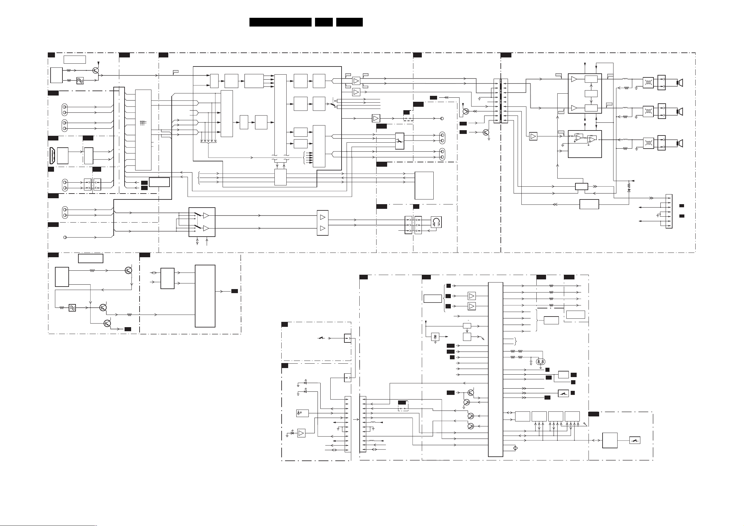
Block Diagrams, Testpoint Overviews, and Waveforms
Block Diagram Audio
AUDIO
IF
B2
SEE ALSO
7323
TDA9321H
B14B
AUDIO IN
AUDIO IN
B14F
1
19
D
AUDIO IN
B14C
AUDIO I N
B14B
B15A
18 2
FRONT
HDMI
CENTRE
BLOCK DIAGRAM
VIDEO
5
HIP
MAIN
10
I/O
1I01
AV2
L+R
1I04
AV1
L+R
DIGITAL INPUT
7I18
SIII9993CT
HDMI
PANELLINK
RECEIVER
SIDE I/O
1002
L+R
1I07
L+R
1I06
IN
PIP IF
7P09
TDA9321H
QSS_AM
PIP
VIFOUT
3P38
3380
(FOR AP)
3437
SPDIF-HDMI
FRONT-L
FRONT-R
10
5
1P07
SOUND-OUTPUT
1411
SND-CENTER-IN
(FOR US)
(FOR AP)
(FOR US)
AL-SC1-IN
AR-SC1-IN
AL-SC2-IN
AR-SC2-IN
B14D
7I18
SIII9993CT
DAC
1M36
10
11
SNR-DVI-IN
SND-DVI-IN
SEE ALSO
BLOCK DIAGRAM
VIDEO
3P26
OR
OR
+8VP
7410
SNDL-BO-OUT
SNDR-BO-OUT
B21
1M36
10
11
7P07-1
7P07-2
QSS_AM
B6a
B6a
3
4
5
6
13
14
10
9
B6a
B6a
B6a
SIF-OUT
PIP-AM
B14D
4
6
14
10
2
11
3
5
13
9
1
12
11
12
2
1
SNDL-SEC-IN
SNDR-SEC-IN
B14D
7P05
3P93
AUDIO I/O
7I17
TEA6422D
25
R1
24
R2
SWITCH
23
R3
20
R4
19
R5
18
R6
4
L1
5
L2
6
L3
9
L4
10
L5
11
L6
PIP-AM
PIP-FM
MATRIX
B15A
B15B
B15B
SDA-S
SCL-S
13
R1
12
L1
15
R2
14
L2
17
R3
16
L3
SEE ALSO
BLOCK DIAGRAM
VIDEO
PIP I/O
3
2
7P55-M
7P56
M62320
AUDIO I/O
B14b
B14c
B14c
I/O
EXP
B65
SND-CENTRE-IN
SNDR-MAIN-IN
SNDL-MAIN-IN
SNDR-DVI-IN
SNDL-DVI-IN
SNDR-SEC-IN
SNDL-SEC-IN
B6a
B6a
SNDR-SC2-OUT
SNDL-SC2-OUT
SEL-PIP-SOUND1
4
SEL-PIP-SOUND2
6
17
18
20
14
13
11
50
47
45
44
42
41
39
38
36
35
7A06
TDA7309
3
7A02
MSP34x1G
IF1
IF2
SC4
N.C.
SDA-F-AUD
7P55
TDA9820T
INTERCARRIER
SOUND
DEMODULATOR
(MONO)
SC1
SC3
I2S-DPL-OUT
I2S-DPL-CLK
I2S-DPL-WS
SCL-F-AUD
FM
ADC
MONO-IN
EN 26FTL2.4A AA 6.
CONNECTIONS
B21
7A03
B68
B66
DE-
MODULATOR
SCART
DSP
INPUT
SELECT
12
15
14
2
9
PRESCALE
PRE-PROCESSING
ADC
PRESCALE
HPN-L
HPN-R
SOURCE
SELECT
INTERFACE
LOUD-
SPEAKER
SOUND
PROCESSING
HEADPHONE/
SURROUND
SOUND
PROCESSING
DAC
DAC
I2S
DAC
DAC
SCART
OUTPUT
SELECT
7A07
MC33178D
3
5
5
6
3
LOUD
DACM-SUB
FRONT-DECT
SC
I2S-MSP-OUT
I2S-MSP-IN
I2S-MSP-CLK
1
7
20
21
B67
23
17
HPN-R
18
HPN-L
18
MSP-CENTER
18
MSP-SURR
DACM-SUB
23
28
29
25
26
HEADPHONE-L
HEADPHONE-R
LM833D
5
3
7A00-A
3
SNDR-SC1-OUT-DC
SNDL-SC1-OUT-DC
7
1
B69
1
SNDR-MON-OUT
SNDL-MON-OUT
AUDIO-R
AUDIO-L
AUDIO-SW
7A00
LM833D
5
7
B14D
B6D
B21
N.C.
N.C.
N.C.
N.C.
AUDIO_SW
I/O 4 AUDIO
7I20
74HC4053
3
1
5
2
AUDIO DELAY
I2S-MSP-OUT
I2S-MSP-IN
I2S-MSP-CLK
CONNECTIONS
N.C.
AUDIO-R
AUDIO-L
IRQ-AUDIOSUPPLY
B5A
I/O
B14D
B6C
9ID0
4
SNDR-SC2-OUT
15
SNDL-SC2-OUT
SNDR-MON-OUT
SNDL-MON-OUT
AUDIO
DELAY
SIDE I/O
D
1M36
1M36
10
10
11
11
7
7
SUBW
HEADPHONE-OUT
L
R
DETECT
1I06
SUB
WOOFER
1I09
AUDIO OUT
L+R
1I05
AUDIO OUT
L+R
+5V2-STBY
B5A
SA
GND-AUD
7010
SOUND-ENABLE
POR
N.C.
AUDIO-SW
7Y01
CONTROLS
OTC FLASH
B21
CONNECTIONS
PIP-FM
8
B14D
E
TOP CONTROL
LED1
SCL-S
SDA-S
+8V
LED2
KEYBOARD
KEYBOARD
RC-IN
0345
2
0345
2
1M20
1M20
1
1
KEYBOARD
2
3
4
5
6
7
8
9
10
11
12
CON-SND
2
LED1
3
RC
4
LIGHT_SENSOR
5
5Y11
6
7
8
9
LED2
9Y06
10
SCL-SF
11
SDA-SF
12
+8V
+5V2-STBY
B14E
9ID0
LED + SWITCH
E
6070
6060
BLUE
6051
1040
IR
SENSOR
7070
LM358P
LIGHT SENSOR
6x
ON / OFF
CHANNEL+
CHANNEL-
VOLUME+
VOLUME-
MENU
RED
LIGHT-SENSOR
72
+5V2-STBY
B5A
SEE ALSO
BLOCK DIAGRAM
VIDEO
+5V2-CON
7005
LF33AB
IN
1
7001
CVBS-TXT
B2
B3A
B3A
OUT
+3V3
INTOTC
B14B
B14B
N.C.
HD3-EPLD
VD-EPLD
CVBS-Y-RECORD-IN
7002 :
7004
RESET
RESET
FLASH
RAM
STATUS_SC3
STATUS_SC4
7015
7016
7013, 7014
B4
N.C.
N.C.
N.C.
CON-SND
P50
B14B
7008
ON-OFFOLED
+3V3
LED2
+3V3
RC
LIGHTSENSOR
SAA5801H
83
OTC
84
7
114
74
RESET
RP
109
108
99POR-FLASH
98IRQ-DIGITAL
93HD@HOME
96IRQ-FTV
118
7009
97
120
7022
115
7022
115
100
107KEYBOARD
110
AUDI O
SA3B6A
1739
1M52
1
1
2
2
3
3
4
4
5
5
6
6
7
7
8
8
9
9
775
78
79
80
88 SDA-F
87 SCL-F
86 SDA-S
85 SCL-S
90 TXD
N.C.
89
RXD
3099-3 3081
119
3074-4 3097
96
104 STANDBY
95 SOUND-ENABLE
94 RESET AUDIO
117
116
103
7011
MC24C32
SDA
5
91
EEPROM
6
92
SCL
ADDRESS
DATA
CONTROL
16
1001
17
6Mhz
R-TXT
G-TXT
B-TXT
FBL-TXT
NVM.
4kByte
AUDIO-R
AUDIO-L
7715
7
3
B3A
SAM
SDM
2016
SEL_IN_2
SEL_IN_1
PWW-BLACKLIGHT
7007
MSM51V18165F
DRAM
(TXT)
16Mbit
I722
I711
I747
SOUND-ENABLE
POR-CLASSD
PROT-AUDIO-SUPPLY
3858
3859
3860
3861
SEE ALSO
IIC DIAGRAM
6005
SA
A-PLOP
B6A
7516
N.C.
74HC4053
B5B
7006
LH28F320BJE
PROGRAM
FLASH-RAM
SET SW
32Mbit
7700
TDA7490
18
6
STBY-MUTE
10
7702
TDA7481
IN
9
FEEDCAP
10
STBY/MUTE
(OPTIONAL)
7701 : 7707
B19C
SEE ALSO
BLOCK DIAGRAM
VIDEO
B14B
SA
H
7012
M29W400BT
EPG-
FLASH-RAM
4Mbit
-16V-19V
-16V-19V
PRE
SOUND
ENABLE
AUDIO
SUPPLY
PROT, CIRCUIT
R-OSD
G-OSD
B-OSD
BL-OSD
RP
+16 +19V
24 22
23
PWM
OSC
3
PWM
24
+16V+19V
14,15 11,13
1
OUT
PWM
DCPROT
PROT1
OTC-FLASH
B5C
(OCTAL BUS TRANSCEIVER)
7018
7019
I778
I776
74LVC245APW
74LVC245APW
AUXILIARY
FLASH
PROGRAM
CIRCUIT
FOR
FLASH RAM
1735
5702
3717
5701
3718
5720
3728
5730
5731
5733
R
1
3
1736
1
3
1738
4
3
15W/
8Ω
L
15W/
8Ω
SUBWOOFER
15W/
8Ω
(OPTIONAL)
+16V+19V
3745
6745
1404
SSSS811
SWITCH FOR
SOFTWARE
DOWNLOAD
DCPROT
+16V+19V
-16V-19V
1M02
7
6
TO 1M02
5
A4
LCD 42"
4
TO 1M02
3
A2
2
LCD 30"/37"
1
F_15500_044.eps
290705
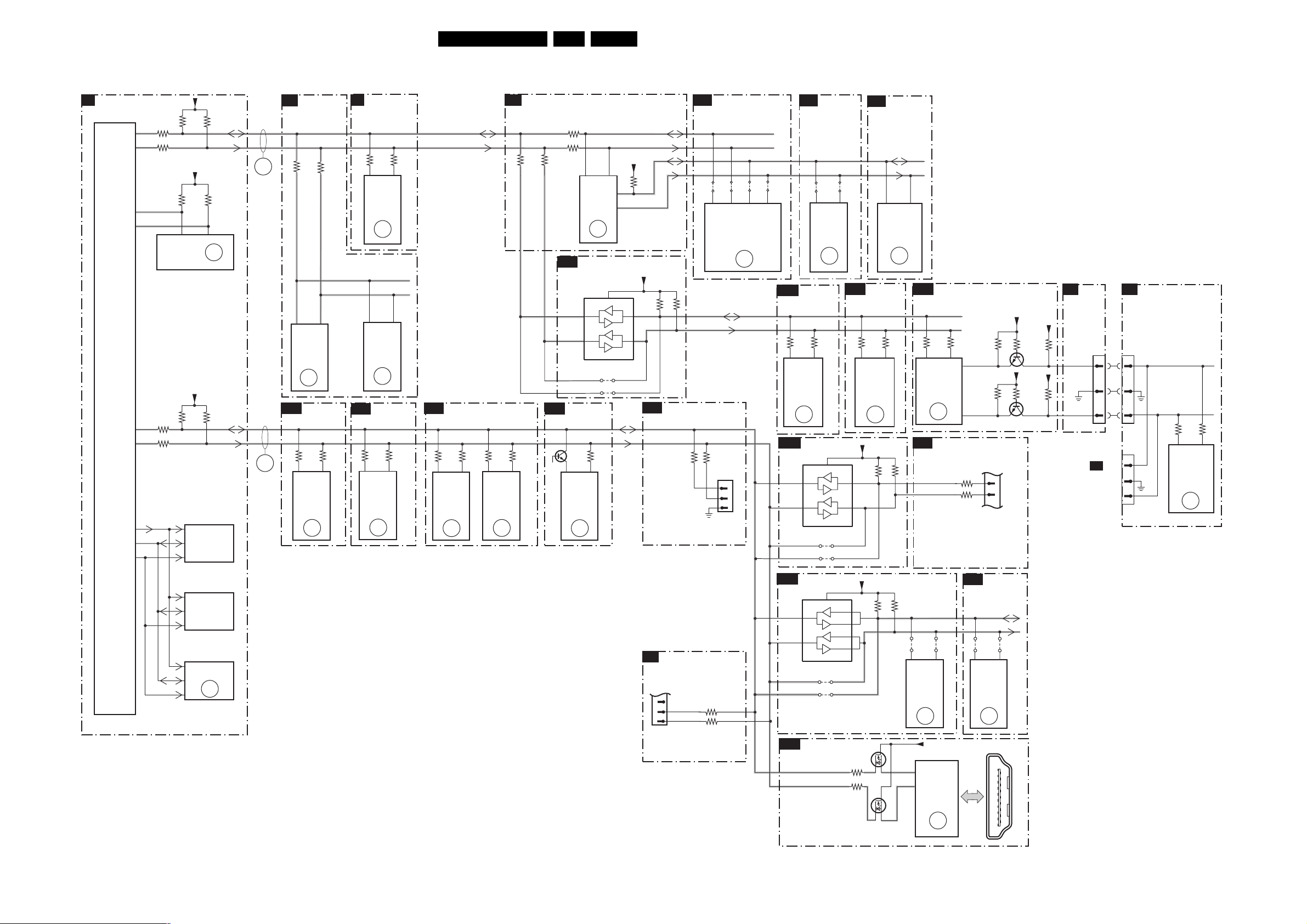
I2C Overview
IIC
OTC
B5
7001
SAA5801H
SET
PROCESSOR
ADDRESS
DATA
CONTROL
Block Diagrams, Testpoint Overviews, and Waveforms
+5V2_CON
3069
3079
ERR
1
+5V2_CON
3092
7006
SDA-F
SCL-F
SDA-S
SCL-S
ERR
18
ERR
6
3064-4
88
3064-3
87
+3V3-INTOTC
SDA
SCL
M24C64
EEPROM
3064-2
3064-1
7011
(NVM)
3001 3002
56
3088
M29W320DT
PROGRAM
FLASH-RAM
91
92
86
85
AUDI O
B6A
DEMODULATOR
3A17
21
7A02
MSP3411G
AUDI O
DEMODUL
ERR
I/O4 AUDIO
B14D
3IJ0
28 27
TEA6422D
DECODER
14
7I17
BUS
ERR
3A19
SDA-F-AUD
3IJ1
21
RES
B2
SCL-F-AUD
B15A
I/O, VIDEO
PROCESSING
TDA9321H
3377 3376
47 46
7323
TDA9321H
HIP
ERR
8
4
7A06
TDA7309D
AUDIO
DECODER
ERR
82
PIP HIP
3P23
47 46
7P09
HIP
ERR
34
5
3P22
PIP SWITCH
B15B
3P66
32
7P56
M62320FP
I/O
EXPANDER
ERR
EN 27FTL2.4A AA 6.
PICNIC
B3A
6
7
3758
3E69
SDA-D
SCL-D
SN-DA
SN-CL
3E70
SDA-F
SCL-F
3826
SDA-EPLD
3827
SCL-EPLD
B19B
3710
3709
EPLD
CONTROL
7E10
PCA9515ADP
3
2
SAA4978H
+5V2Pr
54
7713
1
2
PICNIC
ERR
3
8
VCC
+3V3-EPLD
I2C BUFFER
9E57
RES
9E58
RES
PIP MUPPET
B15C
SDA-S
SCL-S
3P81
14 15
7P51
Z86130
V-CHIP
(US ONLY)
ERR
25
3P79
HA
7PA5
74 73
7PA6
SAB9083H
MUPPET
ERR
24
3PC1
3P65
21
B14E
I/O5
RES
B3D
3IS9
3IS8
SDA-SF
SCL-SF
COMPAIR
SERVICE
CONNECTOR
COLUMBUS
9817 9818
A15 B15
7752-2
T6TU5XB
COLUMBUS
CTRL
SDA-F3
SCL-F3
1M15
1
2
3
ERR
35
9815 9816
C14 D14
B19A
3L06 3L03
57 56
7L01
AD9883AKST
COVERTER
B14E
7I10
PCA9515DP
EAGLE
B3C
9757 9755
33 24
7720
T6TX5AFG
EAGLE1C
ERR
HDI A/D
CONVERTER
A/D
ERR
53
I/05
VCC
3
2
9I06
9I05
FALCONIC
B3B
SN-DA
SN-CL
34 41
7760
SAA4998H/V1
FEM
ERR
EPLD OSD
3E18 3E19
7E23
A/D
ERR
53
3IB3
3IB1
RES
26
EPLD I/0
B19D
3V38 3V37
2
7V01-4
EP1C12F256C8
BANK3
ERR
56
SCREEN
B20
INTERFACE
SDA-DISP
SCL-DISP
1
AL-CL-IN
AL-DA-IN
3Z51
3Z50
1G50
3V50
3V55
31
30
+3V3-IO
3V51
+3V3-IO
3V54
TO
DISPLAY
RES
7V04-1
7V04-2
+5V
3V52
+5V
3V53
CON.
B21
1M51
AL-CL
AL-DA
TO 1M48
2nd AMBI LIGHT
See also
Blockdiagram
Control
11
22
33
AL
AL
1M49
1M48
1
2
3
AMBI LIGHT
3002 3001
6
7001
P87LPC760
MICRO
CONTROLLER
ERR
53
7
27
B19C
57 56
AD9883AKST
COVERTER
+3V3_SIM
8
6
7
7007
MSM51V18165F
DRAM
(TXT)
7012
M29W400DT
ERR
32
CONNECTIONS
B21
1M20
11
12
LED SWITCH
PAN E L
(ITV)
SDA-SF
SCL-SF
3Y09
3Y40
SDA-S
SCL-S
B13A
B14F
7T50
P82B96TD
1
7
MAIN TUNER
8
VCC
RES
9T50
9T12
I/O6 DIGITAL INPUT
9I55
9I56
3
2
5
6
+5V
7I72
D
D
3T05
G
G
7I59
S
S
3T06
9T07
9T08
54
1T01
UV1318ST
MAIN
TUNER
ERR
13
0VCC
7I18
75
SII9993CT100
74
HDMI
PANNELLINK
RECEIVER
ERR
43
SUB TUNER
B13B
9T10
54
1T02
UV1318S
SUB
TUNER
ERR
23
S-SDA-PIP
S-SCL-PIP
9T09
1
18 2
19
F_15500_045.eps
290705
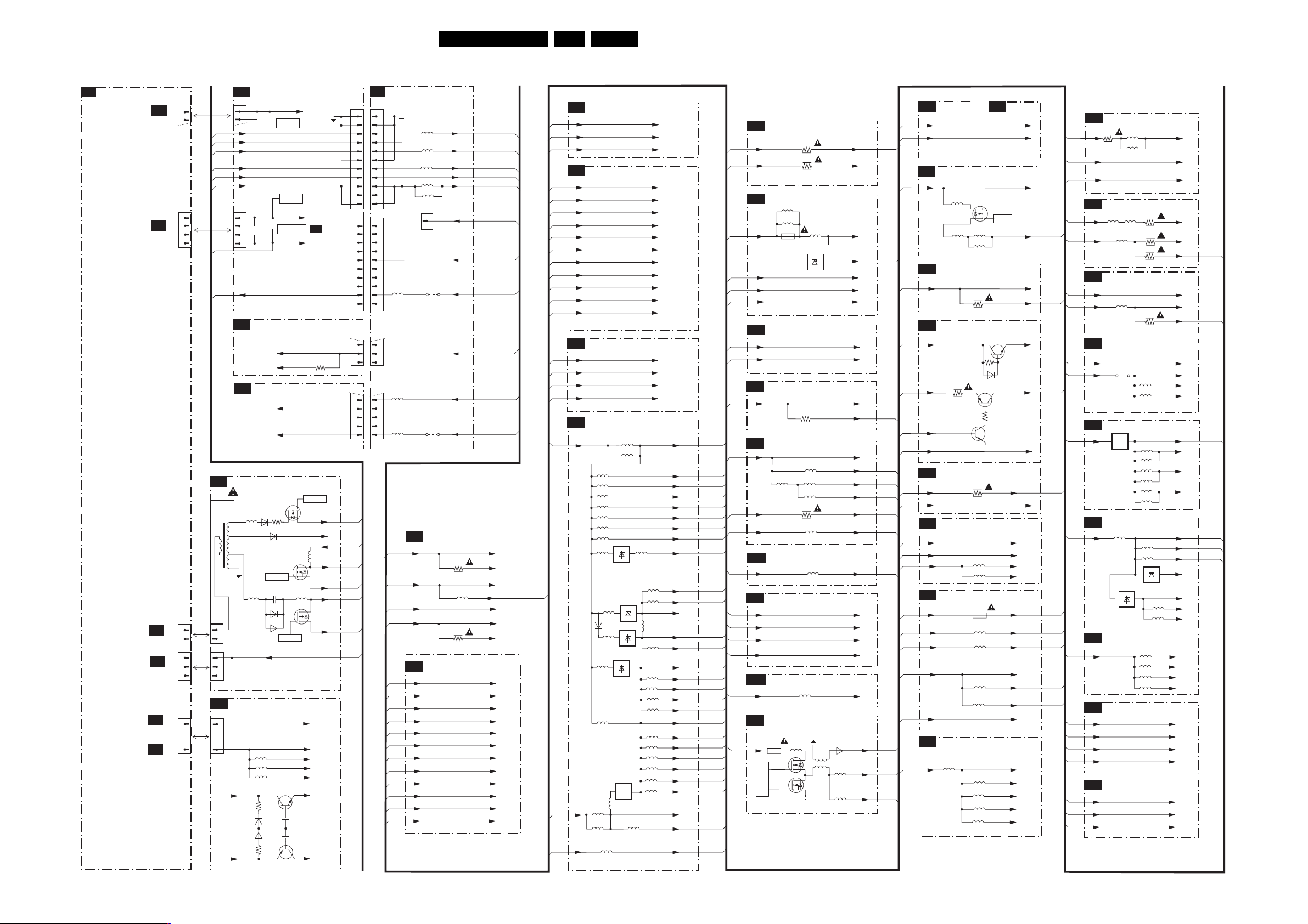
Block Diagrams, Testpoint Overviews, and Waveforms
Supply Lines Overview
SUPPLY LINES
SUPPLY
A
TO 1303
42" SUPPLY
PAR T B
TO 1304
SUPPLY
(PART A 42")
SEE ALSO
BLOCK DIAGRAM
SUPPLY
TO 1306
A1
MAINS FILTER
(PART A 42")
TO 1305
A1
MAINS FILTER
(PART A 42")
TO 1M02
A2
SUPPLY 30"/37"
OR
TO 1M02
A4
SUPPLY 42"
1303
1
A4
2
1304
1
2
A2
3
4
1306
1
2
1305
1
2
3
1M02
6
1
SA2
SA2
SA2
SA2
SA2
SA2
SA2
SA2
5500
1306
1305
SA3
1M02
SA2
1
2
1
2
3
6
1
SA1
1303
1
2
+8V6
+12V
+5V_SW
+5V2
VTUN
+12V
1304
1
2
3
4
+5V2-RELAY-IO2
H
J
STANDBY
6
7
8
10
5
AUDI O
+16V+19V
-16V-19V
CONNECTIONS
SCART 3
+11V_SF
+11V_SFS
LED SWITCH PANEL
6504
3509
5110
6140
CONTROL
2513
5103
6107
6505
+5V2-RELAY-IO2
5723
5707
5711
6719
6719
6719
6719
DISPLAY
DISPLAY
AMBI LIGHT
+8V
+5V2-STBY
7511
7131
7531
CONTROL
7712
6719
6719
7713
+24V_2
Connector
1317
LCD 42”
Connector
1316,1317
LCD 32”
+12V_+24V
+12V_A
3511-3516
CONTROL
5507
5506
+16V+19V
-16V-19V
-Vf21
-Vf11
-Vf1
Vp
Vm
AL
Connector
VTUN
+11V
+12V_A
+12V
+8V6
+5V2
+5V_SW
1M01
1M46
1M03
1M07
1M20
10
SA1
SA1
SA1
SA1
SA1
SA1
SA1
EN 28FTL2.4A AA 6.
CONNECTIONS
B21
1M46
1
1
2
2
3
3
4
4
5
5
6
6
7
7
8
8
9
9
10
10
11
11
1M03
1
2
3
4
5
6
7
8
9
10
1M07
3
4
5
1M20
6
7
8
9
To
Display
1
2
3
SHARP display
4
5
6
7
8
5Y09
9
10
3
4
5
5Y11
6
7
8
9
5Y12
10
B2
+5V_VDP
B14e
+8V
5Y06
+5V
5Y15
+5V2-STBY
5Y07
+33V
5Y02
+11V
5Y03
1M17
+3V3_SIM
1
Only for
+5V
+5V2-STBY
9Y01
+11V_SF
+8V
+5V2-STBY
9Y06
IF,I/O VIDEOPROCESSING
3402
+8V
B21
5416
+5VS
B14e
+8V_VDP
B4
3400
PICNIC
B3A
+3V3_DCDCFBXA
B3e
+1V8FA
B3e
+1V5_FBXA
B3e
+3V3_FBXB
B3e
+2V5_FBXA
B3e
+5V2Pr
B3e
+3V3PA
B3e
+8VPA
B3e
+3V3PB
B3e
+3V3Pr
B3e
+3V3PC
B3e
+3V3GA
B3e
B2,B6a,
B14a,c,d,e,g,B15a
B6a,b,B13a,b,B14b,
c,d,e,B15a,b,19a,d
B5a,B14b,e,
B13a,B13b
B14b,e,B20
B12
B21
B21
B14e
+5V_VDP
+5VCOM
+8V
+8V_CON
+5VS
+8V_VDP
+8VP
+3V3_DCDCFBXA
+1V8FA
+1V5_FBXA
+3V3_FBXA
+2V5_FBXA
+5V2Pr
+3V3PA
+8VPA
+3V3PB
+3V3Pr
+3V3PC
+3V3GA
B21
B21
B3e
B3e
B3e
B3e
B3e
B3e
B3e
B3e
B3e
B3e
B3e
B3e
B3e
B3e
B3e
B3e
B3e
B3e
B12
B3e,B5a,B5b
B6a
B2
FALCONIC EMBEDDED MEMORY
B3B
+3V3FA
+3V3FB
+1V8FA
EAGLE
B3C
+2V5EC
+2V5ED
+1V5EA
+1V5EB
+2V5EA
+2V5EB
+3V3EA
+3V3EB
+3V3EC
+5V2Pr
+3V3ED
COLUMBUS
B3D
+3V3CB
+3V3CA
+1V5CA
+5V2Pr
FBX SUPPLY
B3E
+3V3_DCDCFBX
5767
5779
5768
5769
5770
5771
5773
RES
7773
5772
5709
6719
5760
7774
5775
5777
7774
IN OUT
5764
5721
+5VF
5722
+8V_CON
5702
5719
5720
7701
7770
RES
5775
+3V3FA
+3V3FB
+1V8FA
+2V5EC
+2V5ED
+1V5EA
+1V5EB
+2V5EA
+2V5EB
+3V3EA
+3V3EB
+3V3EC
+5V2Pr
+3V3ED
+3V3CB
+3V3CA
+1V5CA
+5V2Pr
5763
5758
5759
5761
5753
5752
5764
5713
5762
5750
5751
5780
5801
5756
5753
+3V3_DCDCFBXA
+3V3PA
+3V3GA
+3V3PB
+3V3PC
+3V3FA
+3V3FB
+3V3Pr
+1V8FA
+1V5EB
+1V5CA
+1V5_FBXB
+1V5_FBXA
+1V5EA
+2V5_FBXA
+2V5ED
+2V5EC
+2V5EA
+2V5EB
+3V3_FBXB
+3V3EA
+3V3EB
+3V3ED
+3V3EC
+3V3CA
+3V3CB
+5V_FBXA
+5V2Pr
+8VPA
B3a,B3b
B3a,B3c,B3d
HOP
B4
+5V_VDP +5VS
B14e
+8V_VDP +8VS
B14e
OTC FLASH
B5A
3304
3329
5000
B21
B21
B2
B14e
5001
+5V2-STBY
B21
B5c
B2
B5c
B5B
+5V_CON
B14e
+8V_CON
B2
B5C
+3V3_INTOTC
B5a
B3a
B3a
B3a
B3a
B3b
B3b
B3a
B6A
+5V
B21
B3a
+8V
B21
+11V_S
B14b
B6B
+5V
B21
B3c
B3d
B3a
B3c
B3c
B3d
B6C
+5DB
B6a
+8VC
B6a
+11V_AUD
B6a
+5DA
B6a
B3a
B3c
B6D
B3c
+5M
B6b
B3c
B3c
B3a
B12
B3c
B3c
B3c
B3d
B3a
+11V
B21
1000
F500mA
VPP-SW
+8V_CON
EAn
BACKLIGHT CONTROL
BACKLIGHT CONTROL
3C01
AUDIO DEMODULATOR
5A00
5A02
5A03
3A03
DOLBY DIGITAL DECODER
DOLBY PROLOGIC PROCESSOR
AUDIO DELAY
5A07
MAIN TUNER
1U01
5U02
T1500mA
7U04
7U03
CONTROL
5A06
5A01
5A38
5003
7005
RES
5U01
+5V2_CON
+3V3_INTOTC
VPP_SW
+8V_CON
EAn
+3V3_INTOTC
6U02
5U05
5U06
+5V_CON
+8V_CON
EAn
+5V
+5VF
+5DA
+5DB
+8VC
+11V_AUD
+5M
+5DB
+8VC
+11V_AUD
+5DA
+5D
+3V3-LINK
+3V3_SIM
+3V3_
DCDCFBX
B3c
B5a
B3e
B6c
B6c
B6c
B6c
B6b
N.C.
B14d,B15c,
B19b,B20,
B21
B3a,B3c
B21
B21
B21
B21
B21
B21
B14a
B21
B21
B12
B21
B14b
B21
B21
B21
B19a
B13A
MAIN TUNER
B13B
SUB TUNER
+5V
+33V
DC-DC CONVERTER
B13C
+11V_DC
5T10
5T14
7TO4
DC-DC
7T01-1
5T11
5T15
I/O1 MMC
B14A
+8V
3IK7
I/O2 CONNECTIONS
B14B
+5V2-STBY
7I05-1
3I37
+11V
7I07
6I11
3IC1
3ID0
+5V
+8VA
I/O3 SWITCH
B14C
+5V +5VIO
3
1
7I09
2
3IN4
+8V
I/O4 AUDIO
B14D
+8V
+5V
+3V3_SIM
I/O5
B14E
+11V
+11V_S
+8V
+5V
+5V2_STBY
I/O6 DIGITAL INPUTS
B14F
+3V3-AD
5I35
5I54
5I55
1I79
T300mA
5IEE
5I47
5I46
5I45
5I34
5I35
5I32
5I40
+8V
+5V
VDDD
VDDA
+11V_DC
+11V_SF
+8V_VDP
+5V
+5V_CON
+5V_VDP
+5V2_STBY
+3V3-Si
OVCC
AVCC
PVCC2-Si
DACVCC
+5V
+33V
+11V_DC
VDISP
+8V
(MMC)
+8VA
+5V2-SW
+11V_S
+8VA
+8V
B14b
B6a,B14e
B13c
B2,B4
B5a,B5b
B2,B4
B20
B14g
B21
I/O7
B14G
3I40
B21
B14c
B19a
B21
B15b
B21
B21
B15a
B12
B21
+8V
+5VIO
+3V3-AD
B15A
+5V
+8V
B15B
+8VPIP
+5V
B15C
+5VPIP
+3V3_SIM
B19A
+5V
5I13
5I12
PIP HIP
5P01
5P00
3P00
3P01
5P03
3P02
PIP SWITCH
5P51
3P74
PIP MUPPET
9PB2
5PA9
5PB0
HDI A/D CONVERTER
7L02
3
2
2
IN OUT
5L16
5L13
5L17
+8V-VIDEO
+5VIO
+3V3-AD
+5VHIP
+8VHIP
+8VPIP
+8VPIP
+5VD
+5VPIP
+5VPIP
+3.3V
+3V
+3VD
+3V3-AD
VD
VDD
B15b
B15c
B14f,g,B19c
5L14
5L18
PVD
5L15
EPLD CONTROL
B19B
+3V3-SIM
B19C
+3V3-AD
B14eB14e
B19D
+3V3-IO
+3V3-SD
+5V
+3V3_EPLD
B20
+3V3_SIM
VDISP
+11V
5E53
7E05
1
3
EPLD OSD
EPLD I/O
SCREEN INTERFACE
B12
B19a
B19b
B19b
B21
B19b
B12
B13c
B21
5E54
5E51
1
5E00
5E01
5E02
5E03
7E01
3
5E52
5E50
VBL
VDO
VDDO
PVDO
+3V3-IO
+3V3-SD
+5V
+3V3_EPLD
+3V3_SIM
VDISP
+11V
E_14620_140.eps
+3V3-EPLD
+3V3-SD
+3V3-IO
+2V5-IO
+1V5
+1V5-PLL
+1V5-INT
B19d
B19d
B19d
020205
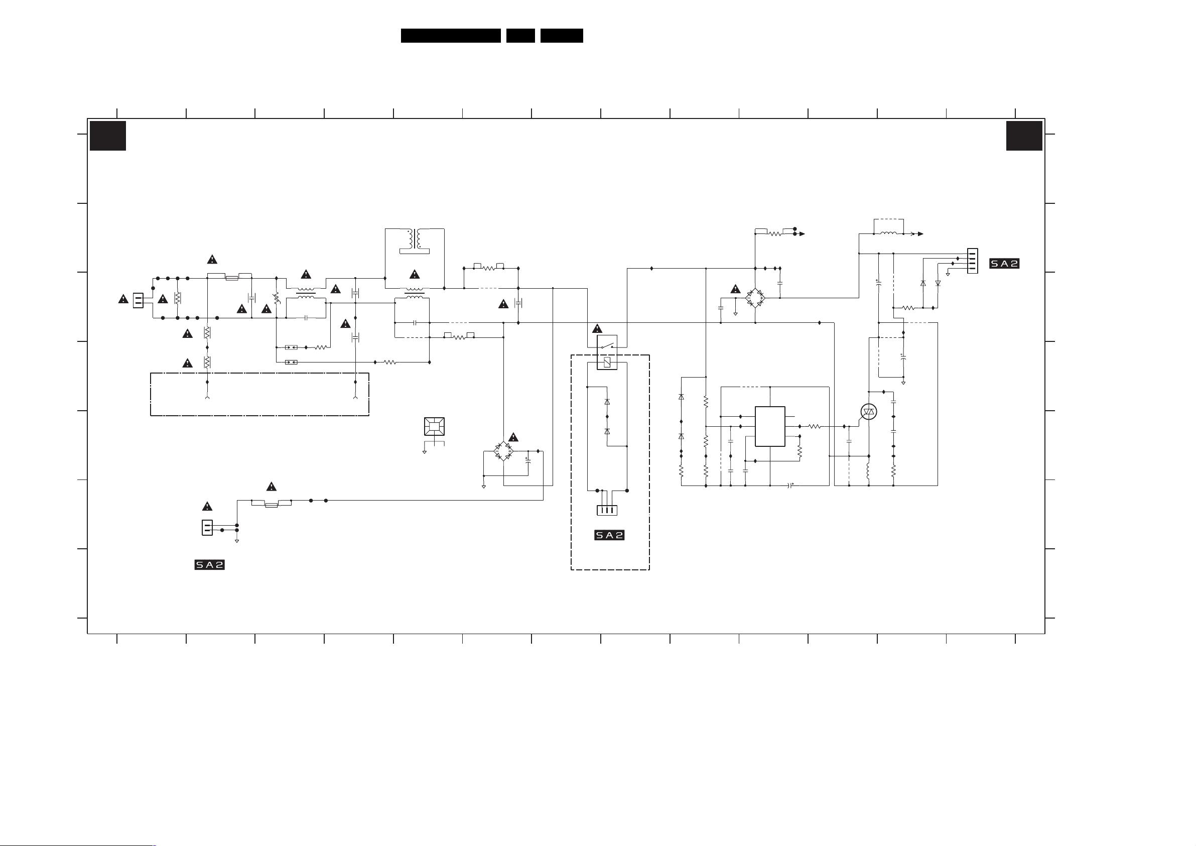
Circuit Diagrams and PWB Layouts
EN 29FTL2.4A AA 7.
7. Circuit Diagrams and PWB Layouts
LCD Supply Panel: Mains Filter + Standby
123456
A1 A1
MAINS FILTER + STANDBY
7
A
MAINS FILTER
5403
1
B
MAINS INPUT
95-264Vac
C
F411
F414
F413
F412
F410
2
1
1308
F415
3401
F418
4M7
F416
F419
D
T3.15AH 250V(EUR)
T5AH 250V(AP)
T5AH 250V(US)
F417
3402
I419
3403
I429
1000
1
GND screw
1400
PTF/65
4M7
4M7
I410
23
3400
V
1403
500V
1402
500V
DMF3547HB60
14
2400
470n
COLD GROUND
5401
2404
47p
I431
3405
220R
2401
I416
2407
I430
1
GND screw
470n
1001
220p
I411
I455
3404
220R
E
T1AE 250V
1401
F
1306
1
2
TO 1306
AUDIO-STANDBY
F426
GNDHOT
F424
F425
PTF/65
F427
F428
290V (303V)
4
2
3
5402
23
14
DMF3547HB60
2406
9003
I412
47p
I432
1011
HEATSINK
9001
3451
I442
3450
1R0
9005
1R0
6506
DF06M
GNDHOT
2408
I415
I444
I445
2503
100n
HOT
1450
G5PA-1-5VDC
I424
I456
4V8 (0V)
10u
RELAY +
F420
1305
TO 1305
AUDIO-STANDBY
COLD
G
3104 313 6063.2
1
234567891011
8 9 10 11 12 13
9050
5006
288V (0)
9814
100n
100n
I824
I826
4R7
2816
2810
2809
3805
6155
3101
1K0
9808
I830
330u
I825
330u
2815
9813
9811
I420
7806
AVS10CB
47n
I422
33u
5804
6461
6460
1
2
BAS316
BAS316
3
COLD
RELAY -
F421
B3B-EH-A
F422
3810
12K
I413
GBJ6J
56n
2804
6809
1N5062
1M0
AVS1ACP08
3800
I814
6808
1N5062
3807
3806
I828
22K
3804
I820
I816
I815
470R
20K
9806
2805
2807
I426
I427
47n
I831
47n
I810
I811
I813
6807
9810
4
7805
VDD
76
MODE
VM
23
OSIN
OSOUT
VSS
1
I428
2802
100p
2803
NC
VG
I812
56n
2806
47u 50V
F423
25V_HOT
I817
I423
3803
58
390R
I425
91K
3802
I421
2808
9812
12 13
400V_HOT
6154
BYG10
I418
I417
BYG10
1307
1
I414
2
3
4
B4P-VH
TO 1307
AUDIO-STANDBY
F_15490_001.eps
120405
F426 F2
1000 D2
F427 F3
1001 D4
1011 E5
F428 F4
1305 F7
I410 B3
1306 F2
I411 C4
1307 B13
I412 C5
1308 C1
I413 B8
1400 C2
I414 B13
1401 F3
I415 C6
1402 D3
1403 D3
1450 C8
2400 C2
2401 C4
2404 C3
2406 C5
2407 C4
2408 C6
2503 E6
2802 E10
2803 C10
2804 C9
2805 E9
2806 F10
2807 E9
2808 E11
2809 E12
2810 D12
2815 C11
2816 D12
3101 C12
3400 C3
3401 C1
3402 C2
3403 D2
3404 D4
3405 D3
3450 B6
3451 C5
3800 D9
3802 E10
3803 E11
3804 E9
3805 E12
3806 E9
3807 E9
3810 B10
5006 B12
5401 C3
5402 C5
5403 B5
5804 E11
6154 C12
6155 C12
6460 E8
6461 D8
6506 E6
6807 C10
6808 E9
6809 D9
7805 D10
7806 E11
9001 C5
9003 C5
9005 C6
9050 B12
9806 E9
9808 C12
9810 D10
9811 D12
9812 E11
9813 C12
9814 C12
F410 C1
F411 B1
F412 B1
F413 B1
F414 B1
F415 C1
F416 C2
F417 C2
F418 C1
F419 C2
F420 F7
F421 F8
F422 B10
F423 B10
F424 F2
F425 F2
I416 C4
I417 B13
I418 C12
I419 D2
I420 D12
I421 E11
I422 E11
I423 E10
I424 E7
I425 E10
I426 E10
I427 E10
I428 E10
I429 D2
I430 D4
I431 D3
I432 D5
I442 B6
I444 B6
I445 C6
I455 D4
I456 E7
I810 B10
I811 B10
I812 B10
I813 B10
I814 E9
I815 E9
I816 E9
I817 C11
I820 F9
I824 E12
I825 E12
I826 E12
I828 E9
I830 C12
I831 E9
A
B
C
D
E
F
G

LCD Supply Panel: Supply
12
16V (0V) for US
20V4 (0V)
25V_HOT
2040
SUPPLY
6081
VS-CONTROLLER
I103
3002
39K
2K7
560p
3003
3004
1234
2034
100p
2035
27K
2009
100p
3043
10R
20V4 (0V)
25V_HOT
2005
3048
I021
3009
100p
2K7
I104
3008
3K3
A2
A
B
C
D
E
F
G
H
I
3104 313 6063.2
2002
BZX384-C22
I006
100p
2004
I009
630V
RES
6001
BAS316
330R
2007
Circuit Diagrams and PWB Layouts
345
3000
4R7
470u
16V (0V) for US
20V4 (0V)
25V_HOT
630V
200p
2006
25V
1n0
3006
3007
10K
16V
470n
I025
3066
10K
3067
100R
I096
I007
I008
10K
I010
3058
5M6
400V_HOT
5017
I027
3005
33K
122V(0V) for US
288V(0V)
3050
820K
SOFTSTART
CONTROL
I018
2027
RES
I022
6020
I143
BAS316
9015
I146
CONTROL
MC34067P
I105
50V
15n
7017
BC857BW
I023
3064
F007
2026
3027
100K
I142
7001
9
1
2
3
16
6
8
7
11
3053
680K
2010
RES
6082
BAS316
9009
I020
10K
50V
2n2
EN|UA
OSCC
OSCR
OSCCC
OS
EAO
Ip
In
SOST
3012
I028
6009
PDZ18-B
I141
100u
I097
15
4
3010
470R
6080
BYG22D
9008 RES
VCC
VREF
OA
OB
PGND
FI
GND
2050
15K
7018
BC847BW
I029
1n0
5
14
12
13
10
I012
3061
PROTECTION
3011
EN 30FTL2.4A AA 7.
6789
HOT GROUND
5008
STP15NK50ZFP
7005
SML4744
I294
400V_HOT
FLM 1/6W
2000V
1n5
c001
I055
I131
16V (0V) for US
20V4 (0V)
25V_HOT
I111
2013
5004
I110
F029
2011
1600V
I034
I149
3100
32
10R
I002
5005
2000V
1n5
1600V
10n
2017
5040
I114
10n
I084
2014
I081
2n2
2000V
BIAS SUPPLY
12V (0V) for US
I095
F004
16V100n
F003
6077
BYG22D
6004
6005
22V(0V)
2003
5015
BAT54 COL
5016
BAT54 COL
F008
I098
I147 I014
6079
BYG22D
2016
3065
100K
68K
CURRENT
I024
2008
470R
16V
470n
6022
BAS316
10K
3013
BZX384-C4V7
6011
2019
I033
6010
BAS316
16V (0V) for US
20V4 (0V)
25V_HOT
I135
3047
BAS316
47R
10n
3068
2K2
6051
I148
I099
2018 RES
2077
I133
2046
6
7
9
GND3
10
I036
100n
2n2
5010
3075
1m0
I039
1K0
47n
I064
BAS316
3019
3K3
3046
6006
BAS316
2062
6008
3028
3020
I100
I101
I045
2n2
3K3
3K3
22R
3021
I140
7004
BC847BW
2048
I052
BAS316
I145
22R
2060
2n2
6003
3035
3K3
3016
3K3
3029
3K3
2065
6002
BAS316
2071
BAS316
1n0
6017
400V_HOT
I109
I004
2n2
1n0
6028
I132
HIGH SIDE
DRIVE
2061
I003
2n2
6007
BAS316
2072
1n0
6027
BAS316
LOW SIDE
100R
3017
I057
47R
3018
I059
I051
BC857BW
7008
GND3
6015
BAS316
I296
6014
BZX384-C22
I295
10K
3089
I011
2047
10n
BAS316
F299
F018
I042
I046
I037
7007
BC857BW
DRIVE
7006
STP15NK50ZFP
6012
SML4744
9025
3055
220R
I001
5007
3014
I038
100R
3015
F002
47R
6013
9024
F005
5013
I113
I112
2012
5041
c002
GND3
F009
2063
I108
I136
470p
2015
10n
I137
9004
50V
100R
3001
BC857BW
4
2
3070
6078
BYG22D
5009
I107
5001
3
S13932-04
22R
3045
I139
7009
I138
1K0
10K
3071
3056
220R
3033
1R0
1m0
470p
2064
I106
I134
HOT GROUND
567
8
COLD GROUND
7002
TCET1102(G)
5002
89
7
6
5
3
2
1
2652.0002 A
2000
470p
F023
F300
COLD GROUND
91011
10 11 12 13
220R
2031
33K
3037
2023
+12V
I119
1
K
A
3
10n
15K
+24V
+12V
470n
RES
RES
3023
15K
R
I094
F293
F294
BAS316
2
DC_PROT
F010
6030
3051
4K7
I089
2030
F292
F290
F295
F001
+12V
A2
11V3 (0V)
14
10V2 (0V)
I116
10
11
12
13
14
15
16
3069
BC847BW
I117
I123
2K2
7030
5027
I070
5028
I073
GND_SND
I076
2290
10n50V
3292
560R
I063
0V (0V)
1n0
3
I072
5025
I077
5026
I124
GND_SND
HEATSINK
I062
I005
470n
2039
2028
50V
6044
STPS20L45CT
2044
50V
1n0
6045
STPS20L45CT
I074
3
I080
12
1007
I292
1009
10K 3031
47K
3032
2
2
2029
50V
1n0
6021
STPS20H100CT
2045
50V
1n0
6025
STPS20H100CT
250V
T5A
372(5.000)
2291
470p
50V
6291
STPS8H100FP
6293
STPS8H100FP
2293
50V
470p
HEATSINK
2
1010
F021
1
2020
13
F012
F024
2
I290
I291
I293
DC_PROT
A2
2m2 25V
F028
F027
F017
F025
1
2022
13
2292
2294
3999
1K0
F016
25V2m2
2021
2038
5293
33u
2m2
5291
33u
2m2
5292
33u
1012
HEATSINK
9010
4m716V
F022
3022
4m7 16V
3030
3057
3052
680R
I120
I085
7010
TS2431
18K
F297
VSND_POS
GND_SND
F298
VSND_NEG
12 13
3049
3054
2024
220n
F014
16V
100n
Vs
Voltage
Adj.
F006
I013
3059
2K2
3036
33K
3044
4K7
470R
BC847BW
I017
2037
470n
7031
3042
12K
I015
ONLY FOR
32" SHARP
I016
24V4 (0V)
2051
220n
2052
220n
2053
220n
2033
220n
33K
3024
MRS25 1%
I088
6023
16V
BAS316
1%
1K8
3025
I093
I092
470R
RES
3034
1%
3026
F296
1M02
7
6
5
4
3
2
1
1304
1
2
3
4
1309
1
2
3
6054
470n
2036
100K
BZX384-C10
1K0
3039
I150
2041
220n
2042
220n
2043
220n
2025
220n
2032
I121
8K2
3040
3041
9002
3038
33K
TO 1M02
AUDIO - STBY
TO 1304
AUDIO - STBY
TO 1309
AUDIO - STBY
F_15490_002.eps
120405
+24V
I122
1007 G10
3044 A13
1009 H10
3045 F6
1010 H11
3046 F6
1012 H11
3047 H5
1304 H13
3048 D2
1309 I13
3049 A12
1M02 G13
3050 E3
2000 E9
3051 B12
2002 A2
3052 C12
2003 A5
3053 E3
2004 C2
3054 C12
2005 D2
2006 C2
2007 E2
2008 F4
2009 D1
2010 H3
2011 E9
2012 E8
2013 C8
2014 F9
2015 F5
2016 E4
2017 D9
2018 F6
2019 H4
2020 C11
2021 B11
2022 E11
2023 A12
2024 E12
2025 E13
2026 G3
2027 E3
2028 B10
2029 D11
2030 F12
2031 B12
2032 E13
2033 E13
2034 C1
2035 C2
2036 A13
2037 B13
2038 D11
2039 B10
2040 C1
2041 D13
2042 D13
2043 D13
2044 C10
2045 E11
2046 I6
2047 I7
2048 I6
2050 E3
2051 D13
2052 D13
2053 D13
2060 C6
2061 B7
2062 D6
2063 C5
2064 D5
2065 D7
2071 E7
2072 C7
2077 H6
2290 G10
2291 G11
2292 G11
2293 H11
2294 H11
3000 A2
3001 G5
3002 C1
3003 C1
3004 D1
3005 C3
3006 D2
3007 E2
3008 E2
3009 E2
3010 H4
3011 H4
3012 F3
3013 F4
3014 B7
3015 C7
3016 C7
3017 D7
3018 E7
3019 F6
3020 E6
3021 F6
3022 C11
3023 E12
3024 E13
3025 F13
3026 G13
3027 G3
3028 E6
3029 C7
3030 F11
3031 A11
3032 B10
3033 A5
3034 F13
3035 C7
3036 A13
3037 C12
3038 E13
3039 A13
3040 E13
3041 F13
3042 B13
3043 D1
3055 I7
3056 I6
3057 A12
3058 E2
3059 A13
3061 E4
3064 F3
3065 E4
3066 F2
3067 H2
3068 G5
3069 A10
3070 H5
3071 H6
3075 G6
3089 H7
3100 A9
3292 G10
3999 A11
5001 C6
5002 C9
5004 C8
5005 C9
5007 B8
5008 B8
5009 B5
5010 A6
5013 D8
5015 C5
5016 D5
5017 A3
5025 D10
5026 E10
5027 B10
5028 C10
5040 D9
5041 E8
5291 G11
5292 H11
5293 G11
6001 D2
6002 D7
6003 C6
6004 C5
6005 D5
6006 I6
6007 C7
6008 D6
6009 H3
6010 F4
6011 F4
6012 E7
6013 C8
6014 H7
6015 G7
6017 I7
6020 H3
6021 D11
6022 H4
6023 E13
6025 E11
6027 C7
6028 E7
6030 A12
6044 B10
6045 C10
6051 H5
6054 A13
6077 A5
6078 A6
6079 A4
6080 A4
6081 A2
6082 A3
6291 G11
6293 G11
7001 C3
7002 A9
7004 H6
7005 C8
7006 D7
7007 C7
7008 F7
7009 G6
7010 E12
7017 F3
7018 F3
7030 A10
7031 B13
9002 G13
9004 B5
9008 A4
9009 A3
9010 C11
9015 H3
9024 C8
9025 E7
F001 H12
F002 C8
F003 C4
F004 D4
F005 D8
F006 I12
F007 F3
F008 D5
F009 D5
A
B
C
D
4n7
RES
E
33K
RES
F
G
H
I
F010 H12
F012 D11
F014 F12
F016 B11
F017 D11
F018 B7
F021 A11
F022 A12
F023 F9
F024 D11
F025 D11
F027 C11
F028 C11
F029 D8
F290 G12
F292 G12
F293 G12
F294 H12
F295 H12
F296 G13
F297 G12
F298 H12
F299 B7
F300 F9
I001 B8
I002 B9
I003 B6
I004 D7
I005 A10
I006 B2
I007 C2
I008 C2
I009 C2
I010 D2
I011 H7
I012 D4
I013 A13
I014 A13
I015 A13
I016 A12
I017 B13
I018 E3
I020 E3
I021 E2
I022 F3
I023 F3
I024 F4
I025 F2
I027 C3
I028 G3
I029 G4
I033 F5
I034 F8
I036 F6
I037 C7
I038 B8
I039 D6
I042 B7
I045 C6
I046 C7
I051 E7
I052 D6
I055 F8
I057 E7
I059 E7
I062 A10
I063 A10
I064 B6
I070 B10
I072 C10
I073 D10
I074 D10
I076 E10
I077 D10
I080 F10
I081 F9
I084 F9
I085 E12
I088 E13
I089 E12
I092 F13
I093 F13
I094 F12
I095 A4
I096 A3
I097 A3
I098 A5
I099 A6
I100 A6
I101 A6
I103 C1
I104 D2
I105 E3
I106 G5
I107 C5
I108 D5
I109 C7
I110 D8
I111 C8
I112 E8
I113 E8
I114 D9
I116 C10
I117 C10
I119 C12
I120 C12
I121 E13
I122 E13
I123 F10
I124 G10
I131 I8
I132 I7
I133 I6
I134 I5
I135 G5
I136 H5
I137 G5
I138 H6
I139 G6
I140 G6
I141 H3
I142 H3
I143 H3
I145 E7
I146 A3
I147 A4
I148 A5
I149 A9
I150 B13
I290 G11
I291 G11
I292 H10
I293 H11
I294 C8
I295 H7
I296 G7
c001 F8
c002 F8
 Loading...