

Philips FTF3020-M-TG, FTF3020-M-IG, FTF3020-M-HG, FTF3020-M-EG Datasheet

IMAGE SENSORS
FTF3020-M
Full Frame CCD Image Sensor
Product specification 1999 November 22
File under Image Sensors
Philips
Semiconductors
Philips Semiconductors Product specification
Full Frame CCD Image Sensor FTF3020-M
• 35mm film compatible image format (36 x 24 mm2)
• 6M active pixels (3072H x 2048V)
• Progressive scan
• Excellent anti-blooming
• Variable electronic shuttering
• Square pixel structure
• H and V binning
• 100% optical fill factor
• High linear dynamic range (>72dB)
• High sensitivity
• Low dark current and fixed-pattern noise
• Low read-out noise
• Data rate up to 36 MHz
• Mirrored, split and four quadrant read-out
• Perfectly matched to visual spectrum
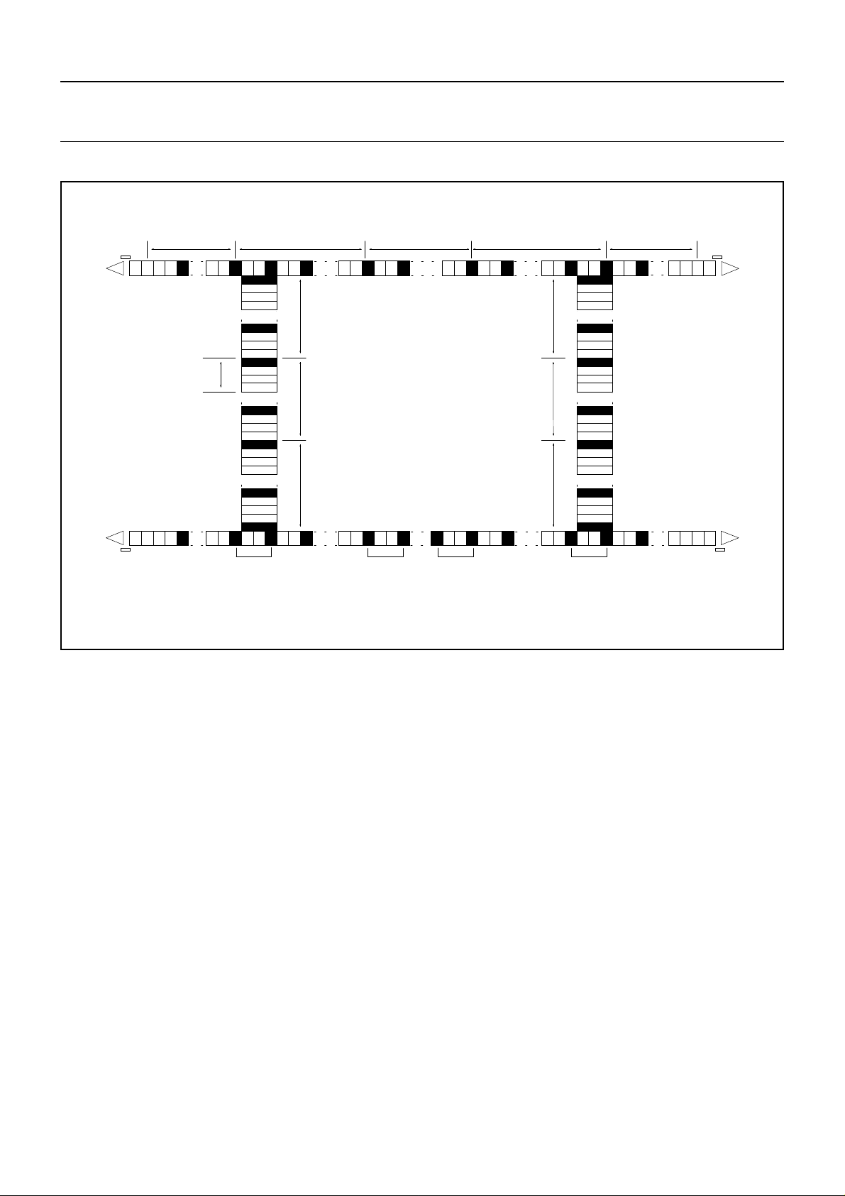
Device structure
Optical size: 36.864 mm (H) x 24.576 mm (V)
Chip size: 39.148 mm (H) x 26.508 mm (V)
Pixel size: 12 µm x 12 µm
Active pixels: 3072 (H) x 2048 (V)
Total no. of pixels: 3120 (H) x 2060 (V)
Optical black pixels: Left: 20 Right: 20
Timing pixels: Left: 4 Right: 4
Dummy register cells: Left: 7 Right: 7
Optical black lines: Bottom: 6 Top: 6
Description
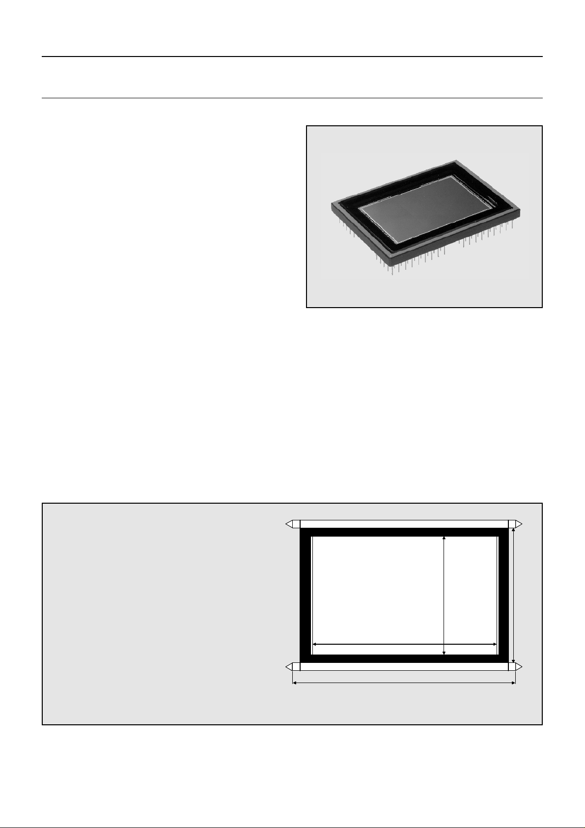
The FTF3020-M is a full frame CCD monochrome image sensor
designed for professional digital photogr aphy applications, with v ery
low dark current and a linear dynamic range of over 12 true bits at
room temperature. The f our lo w-noise output amplifiers, one at each
corner of the chip, make the FTF3020-M suitable for a wide r ange of
high-end visual light applications. With one output amplifier, a
progressively scanned image can be read out at 5 frames per second.
By using multiple outputs the frame rate increases accordingly. The
device structure is shown in figure 1.
Z
Image Area
6 black lines
2048
active
lines
Y
2060
lines
W
Figure 1 - Device structure
1999 November 2
20 20
7
Output amplifier
3072 active pixels
6 black lines
3120 cells
Output register
3134 cells
44
X
7

Philips Semiconductors Product specification
Full Frame CCD Image Sensor FTF3020-M
Architecture of the FTF3020-M
The optical centres of all pixels in the image section form a square
grid. The charge is generated and integrated in this section. Output
registers are located below and above the image section for readout. After the integration time, the image charge is shifted one line
at the time to either the upper or lower register or to both
simultaneously, depending on the read-out mode. The left and the
right half of each register can be controlled independently. This
IMAGE SECTION
Image diagonal (active video only)
Aspect ratio
Active image width x height
Pixel width x height
Geometric fill factor
Image clock pins
Capacity of each clock phase
Number of active lines
Number of black reference lines
Number of dummy black lines
Total number of lines
Number of active pixels per line
Number of overscan (timing) pixels per line
Number of black reference pixels per line
Total number of pixels per line
44.30 mm
3:2
36.864 x 24.576 mm
12x12 µm
100%
16 pins (A1..A4)
7.5nF per pin
2048
4 (=2x2)
8 (=2x4)
2060
3072
8 (2x4)
40 (2x20)
3120
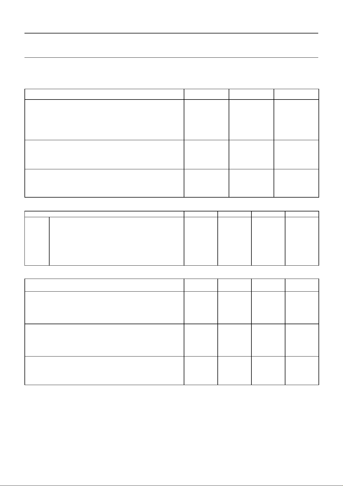
enables either single or multiple read-out. During vertical transport,
the C3 gates separate the pixels in the register . The central C3 gates
of the lower and upper registers are part of the left half of the sensor
(W and Z quadrants respectively). Each register can be used for
vertical binning. Each register contains a summing gate at both ends
that can be used for horizontal binning (see figure 2).
2
2
Output buffers on each corner
Number of registers
Number of dummy cells per register
Number of register cells per register
Output register horizontal transport clock pins
Capacity of each C-clock phase
Overlap capacity between neighbouring C-clocks
Output register Summing Gates
Capacity of each SG
Reset Gate clock phases
Capacity of each RG
OUTPUT REGISTERS
Three-stage source follower
2
14 (2x7)
3134 (3120+14)
6 pins per register (C1..C3)
200 pF per pin
40pF
4 pins (SG)
15pF
4 pins (RG)
15pF
1999 November 3
Philips Semiconductors Product specification
Full Frame CCD Image Sensor FTF3020-M
RGRG
OG
C3 C3 C3 C3 C3 C3 C3 C3 C3C3 C3
7 dummy pixels
RD
OUT_Z
One Pixel
SG: summing gate
OG: output gate
RG: reset gate
RD: reset drain
OUT_W
OG C1 OG
RG
RD
C3 C3 C3C3 C3 C3 C3 C3 C3 C3 C3C3
SG
20 black &4 timing
columns
C1C1SG C2 C2 C2 C1 C2 C1 C2 C1 C2 C1 C2 C2C1 C1 C2 C1 C2 C1 C2 C1 C2 C1 SG OGC1 C3
A1 A1
A2
A3
A4
A1
A1
A2
A3
A4
A1
A2
A3
A4
A1
A1
A2
A3A3
A4
A1
A2
A3
A4
A1
A1
A2
A3
A4
C1C1C2 C2 C2 C1 C2 C1 C2C1
6 black
lines
2K active
images
lines
6 black
lines
C2 C1 C2 C1 C2 C2C1 C1 C2 C1 C2 C1 C2
column
1
column
24 + 1
3K image
pixels
IMAGE
3K x 2K
FF CCD
column
24 + 3K
20 black & 4 timing
columns
column
24 +3K +24
7 dummy pixels
A2
A3
A4
A1
A1
A2
A3
A4
A1
A2
A3
A4
A1
A1
A2
A3
A4
A1
A2
A3
A4
A1
A1A1
A2
A3
A4
A1A1
A1, A2, A3, A4: clocks of image section C1, C2, C3: clocks of hor izontal registers
C1 SG
RD
OUT_Y
OUT_X
RD
RG
RG
Figure 2 - Detailed internal structure
1999 November 4
Philips Semiconductors Product specification
Full Frame CCD Image Sensor FTF3020-M
Specifications
ABSOLUTE MAXIMUM RATINGS
GENERAL:
storage temperature
ambient temperature during operation
voltage between any two gates
DC current through any clock phase (absolute value)
OUT current (no short circuit protection)
VOLTAGES IN RELAT ION TO VPS:
VNS, SFD, RD
VCS, SFS
all other pins
VOLTAGES IN RELAT ION TO VNS:
SFD, RD
VCS, SFS, VPS
all other pins
2
VNS
VPS
SFD
SFS
VCS
OG
RD
3
N substrate
P substrate
Source Follower Drain
Source Follower Source
Current Source
Output Gate
Reset Drain
DC CONDITIONS
1
MIN. MAX. UNIT
-55
-40
-20
-0.2
0
-0.5
-8
-5
-15
-30
-30
+80
+60
+20
+2.0
10
+30
+5
+25
+0.5
+0.5
+0.5
°C
°C
V
µA
mA
V
V
V
V
V
V
MIN. [V] TYPICAL [V] MAX. [V] MAX. [mA]
18
1
16
0
-5
4
13
24
3
20
0
0
6.5
15.5
28
7
24
0
3
8
18
15
15
4.5
1
-
-
-
AC CLOCK LEVEL CONDITIONS
2
MIN. TYPICAL MAX. UNIT
IMAGE CLOCKS:
A-clock amplitude during integration and hold
A-clock amplitude during vertical trans port (duty cycle=5/8)
A-clock low level
Charge Reset (CR) level on A-clock
5
4
8
10
-5
10
14
0
-5
V
V
V
V
OUTPUT REGISTER CLOCKS:
C-clock amplitude (duty cycle during hor. trans port = 3/6)
C-clock low level
Summing Gate (SG) amplitude
Summing Gate (SG) low level
4.75
2
5
3.5
10
3.5
5.25
10
V
V
V
V
OTHER CLOCKS:
Reset Gate (RG) amplitude
Reset Gate (RG) low level
Charge Reset (CR) pulse on Nsub
1
During Charge Reset it is allowed to exceed maximum rating levels (see note 5).
2
All voltages in relation to SFS.
3
To set the VNS voltage for optimal Ver tical Anti-Blooming (VAB), it should be adjustable between minimum and maximum values.
4
Three-level cloc k is preferred for maximum charge; the swing during vertical transport should be 4V higher than the voltage during integration.
A two level clock (typically 10V) can be used if a lower maximum charge handling capacity is allowed.
5
Charge Reset can be achieved in two ways:
5
5
0
10
3
10
10
10
V
V
V
• The typical A-clock low level is applied to all image clocks; for proper CR, an additional Charge Reset pulse on VNS is required (preferred).
• The typical CR level is applied to all image clocks simultaneously.
1999 November 5
 Loading...