Philips DPTV400 Schematic

PHILIPS
PHILIPS SERVICE AND QUALITY
DPTV400 SERIES
HD PTV
TRAINING MANUAL
PHILIPS
TECH
FORCE TRAIN
MANUALS
PHILIPS TECHNICAL TRAINING/QUALITY
ONE PHILIPS DRIVE
PO BOX 14810
KNOXVILLE, TN 37914-1810
PHONE: 865-521-4397
FAX: 865-521-4818
TRAINING
EMAIL: TECHNICAL.TRAINING@PHILIPS.COM

Table of Contents
Introduction
Set Operation Highlights................................................................................................................2
Picture formats ..............................................................................................................................3
Native format............................................................................................................................3
4x3 format ................................................................................................................................3
Panoramic format.....................................................................................................................3
Zoom feature............................................................................................................................3
Tuning the ATSC channels ............................................................................................................4
Overall Power Block ......................................................................................................................8
AC Input.........................................................................................................................................9
Standby Power Supply ..................................................................................................................9
Main Power Supply .......................................................................................................................10
Power Fail detection circuit ...........................................................................................................13
ATSC Power Interface for HD version...........................................................................................14
Epic Power Interface .....................................................................................................................15
Horizontal Output circuit ...............................................................................................................16
High Voltage and Dynamic drive ...................................................................................................16
Vertical Amplifier ............................................................................................................................16
Sweep Failure detection and Blanking ..........................................................................................20
Video Signal Flow block ................................................................................................................21
Side Jack Panel ............................................................................................................................21
NTSC AV inputs and switching......................................................................................................21
NTSC SSB Processing .................................................................................................................25
ATSC block diagram - HD Version ................................................................................................25
ATSC Block diagram - Epic version ..............................................................................................25
HD-DW module signal flow ..........................................................................................................30
YUV to Y Pb Pr Converter ............................................................................................................31
AV3 and AV4 Inputs and Switching ...............................................................................................33
Scaler Block...................................................................................................................................34
SSM video drive ............................................................................................................................36
Sharpness Control ........................................................................................................................37
Tint Control ....................................................................................................................................37
CRT drive.......................................................................................................................................37
HOP IO ..........................................................................................................................................41
CRT panel......................................................................................................................................41
Audio Signal flow...........................................................................................................................43
SSB Sound processor ...................................................................................................................43
Audio Amplifier...............................................................................................................................43
Shutdown Mute..............................................................................................................................47
Convergence processor ................................................................................................................48
Intellisense Convergence correction ............................................................................................48
Intellisense Sensing Circuit ...........................................................................................................48
Convergence Horizontal Output ...................................................................................................51
Convergence Vertical Output ........................................................................................................51
Set Control and I2C Busses ..........................................................................................................54
OSD Signal Path ...........................................................................................................................54
Troubleshooting.............................................................................................................................57
Picture problems............................................................................................................................57
Audio Problems .............................................................................................................................58
Service Modes...............................................................................................................................61

Customer Service Mode ...........................................................................................................61
Service Default Mode ....................................................................................................................62
Service Alignment Mode (SAM) ...............................................................................................62
Manual Alignment of the HD_DW module.....................................................................................63
Equipment required .......................................................................................................................64
Offset Adjustments ........................................................................................................................64
Gain Adjustments ..........................................................................................................................64
Gray Scale Alignment....................................................................................................................65
Error Codes...............................................................................................................................66
Convergence Mode .......................................................................................................................69
Touch Up Convergence...............................................................................................................70
Green Geometry..........................................................................................................................70
Glossary of Terms..........................................................................................................................72
Introduction
The IHDTV2K4 is designed to be marketed in the 2004 model year. This set has a fully integrated
ATSC/NTSC tuning system. This set will tune all of the channels in the NTSC, ATSC, and Cable
bands. There are two RF inputs that are for Cable and Antenna.
The set comes in three versions: the HD, Epic, and Epic Plus. The HD version has the ATSC/NTSC
tuning system. The Epic and Epic Plus versions have two added 1394 inputs. The Epic Plus version also has a Center Channel Amplifier switch which allows the set's speakers to connect to an
external amplifier.
HD Series
Model Chassis
51PP9910/17 DPTV410
55PP9910/17 DPTV410
Epic Series
51PP9920/17 DPTV415
55PP9920/17 DPTV415
60PP9920/17 DPTV415
It also has NTSC composite and SVHS inputs on AV1 and AV2. AV3 and AV4 can accept
Component signals for either 1Fh (NTSC), 2Fh (480p), 720p, or 1080i. AV3 can be either
Component signal or RGB with separate Horizontal and Vertical sync. AV5 is a HDMI digital video
input. Regardless of the input, the signal to be displayed is converted to 1080i.
Analog Left and Right audio is available on the Output monitor line. This can be either fixed or
variable as selected by the user. Coax digital audio output is available on the S/PDIF OUT line.
The Customer can select either Dolby or PCM output. The set has a 20-watt stereo amplifier.
A ComPair port is available to aid the Technician in troubleshooting the set. The ComPair box and
program are required to communicate with the set.
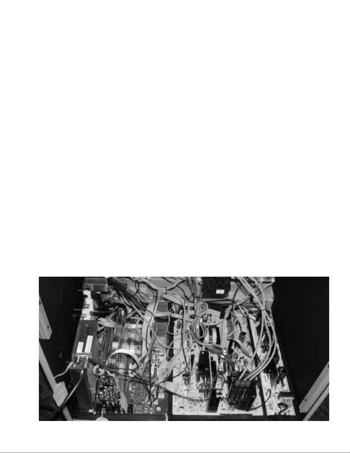
Page 1 REAR VIEW - HD VERSION
Set Operation Highlights
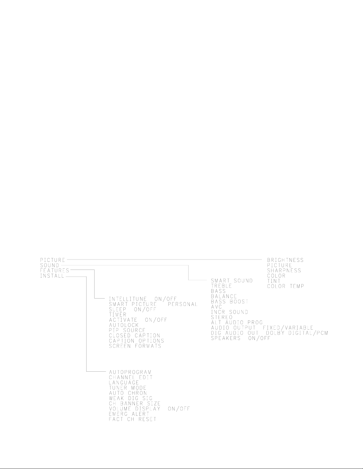
Figure 1 shows an outline of the Customer menus. Listed below are some of the differences from
previous Philips Projection sets.
In the Picture menu selection, there are the normal controls, Brightness, etc. The COLOR TEMP
selection shifts the color balance of the picture when selected by the Customer. The Warm setting
shifts the white balance to the Red. The Cool setting shifts the white balance of the picture to the
Blue. In the Normal setting, the color temperature of the picture shows the picture with the correct
colors. When a gray scale or black and white picture is shown, there will be no color tint in the picture.
The INTELLITUNE selection under Features will auto-program the channels to add any new channels that may be detected while the set is turned Off. This feature can be switched On or Off by the
Customer. It will not delete any existing channels. The Channel Edit selection under Install is used
to manually install the NTSC channels that are not detected by the AUTOPROGRAM. The WEAK
DIG SIG selection is used to add any digital channels that were not detected by the AUTOPROGRAM selection. To delete all of the channels, use the FACT CH RESET selection (channels are
not deleted when the AUTOPROGRAM selection is made).
In the ATSC system, Emergency alerts can be transmitted as low level or high level. The EMERG
ALERT selection in the menu allows the Customer to turn the low level or high level alert feature On
or Off.
FIGURE 1 - CUSTOMER MENUS
Page 2
Picture formats
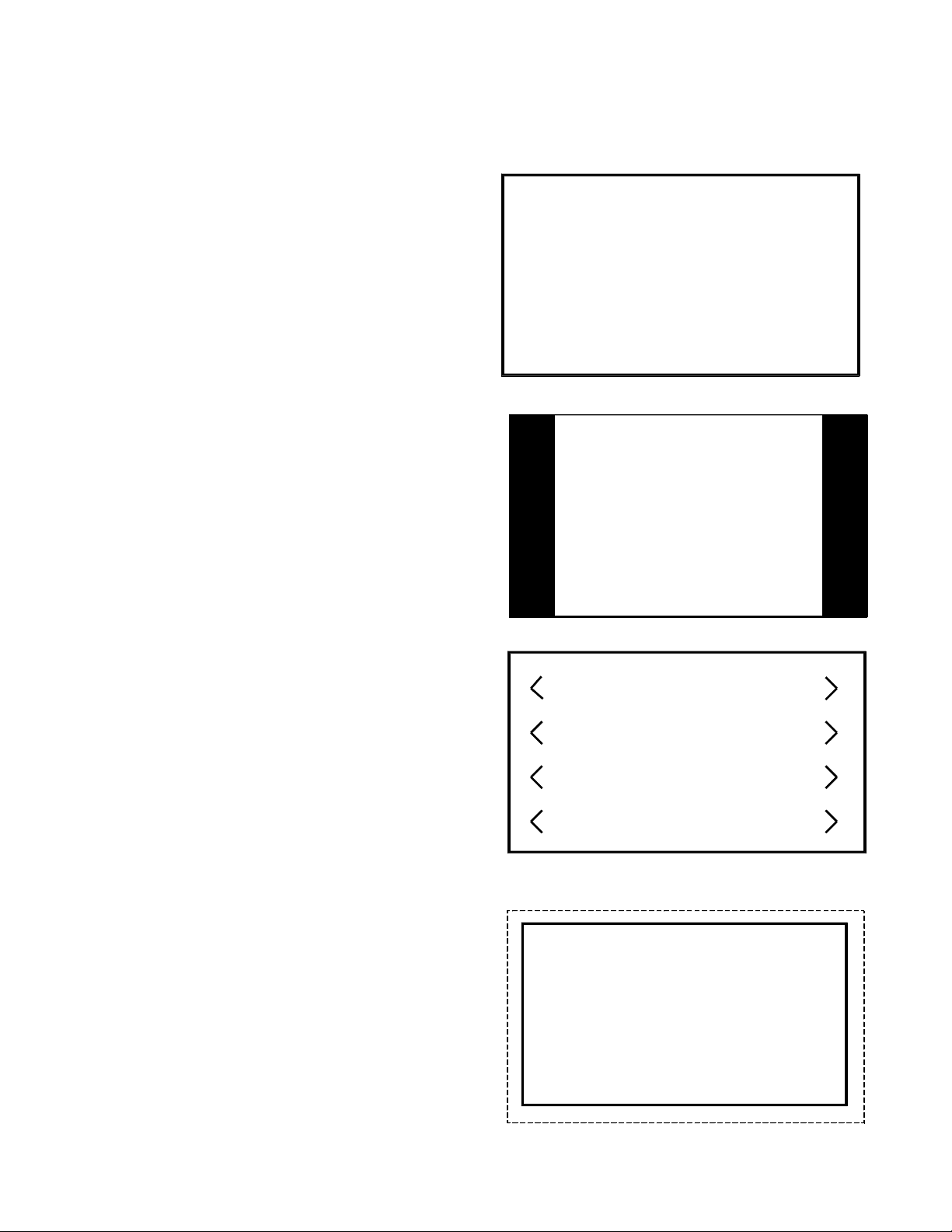
Unlike previous sets, the Picture format can be changed without regard to the input.
Native format
The Native format fills the set’s 16 x 9 screen. If
the source picture is in the 4 x 3 format, the set
will stretch the picture to fill the 16 x 9 screen.
4 x 3 format
The 4 x 3 format displays the picture in 4 x3 with
black bars on each side. The bars slowly shift to
prevent CRT burn in.
Panoramic format
The Panoramic format keeps the picture center
linear while stretching the outside edges of the
picture. This allows a 4 x 3 picture to be displayed on a 16 x 9 screen with minimum linear
distortion.
Zoom Format
The Zoom format expands the picture vertically
and Horizontally. This mode is used when the
original picture is in the letterbox format (black
bars on the top and bottom).
Page 3
Tuning the ATSC channels
When the Autoprogram is selected (see Figure 1), both the ATSC and
NTSC channels are tuned.
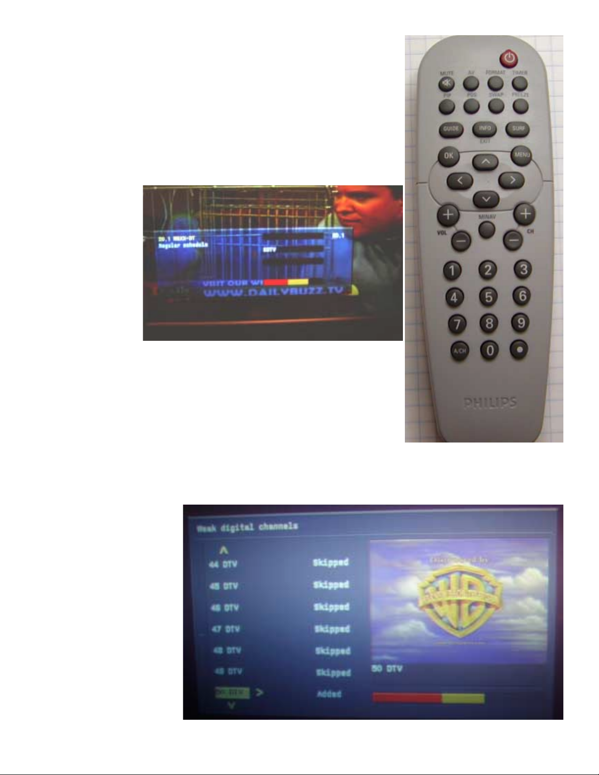
When the Info button is pressed on the Remote, an information box
will appear as show below. The channel number is shown in the left
part of the box. In the center of the box, the type of channel is displayed. If the channel is an ATSC channel, it will display HDTV. If the
channel is a High Definition channel, it will display SDTV if the channel
is a Standard
Definition channel.
If the channel is an
ATSC channel, the
channel’s call letters and program
list will be displayed if the channel is broadcasting
that information.
The channel number indicated in the
display may not be
the actual frequency being received. In the lower part of the box, signal level is indicated. If the bar is all red, there is not enough signal
detected to properly display the channel. When the red bar ends, a
yellow bar will show. This indicates that enough signal is present to
display the channel, but that it is weak. If a strong signal is present, a
green bar will appear to the right of the red/yellow bar. This indicates
that there is enough signal present to display the signal without problems. If the channel is NTSC, the signal level bar and schedule information will not appear.
Weak Digital Channels can be added to deleted from the program list when the Weak Digital Signal
selection is made in the
main menu (see Figure 1).
Use the cursor up/down
button on the Remote to
select the channels. If a
channel is present, the signal level will be indicated.
If the signal is strong
enough, a picture will be
displayed. Use the cursor
right/left buttons to add or
delete the channel. These
menus are generated by
the ATSC module.
Page 4
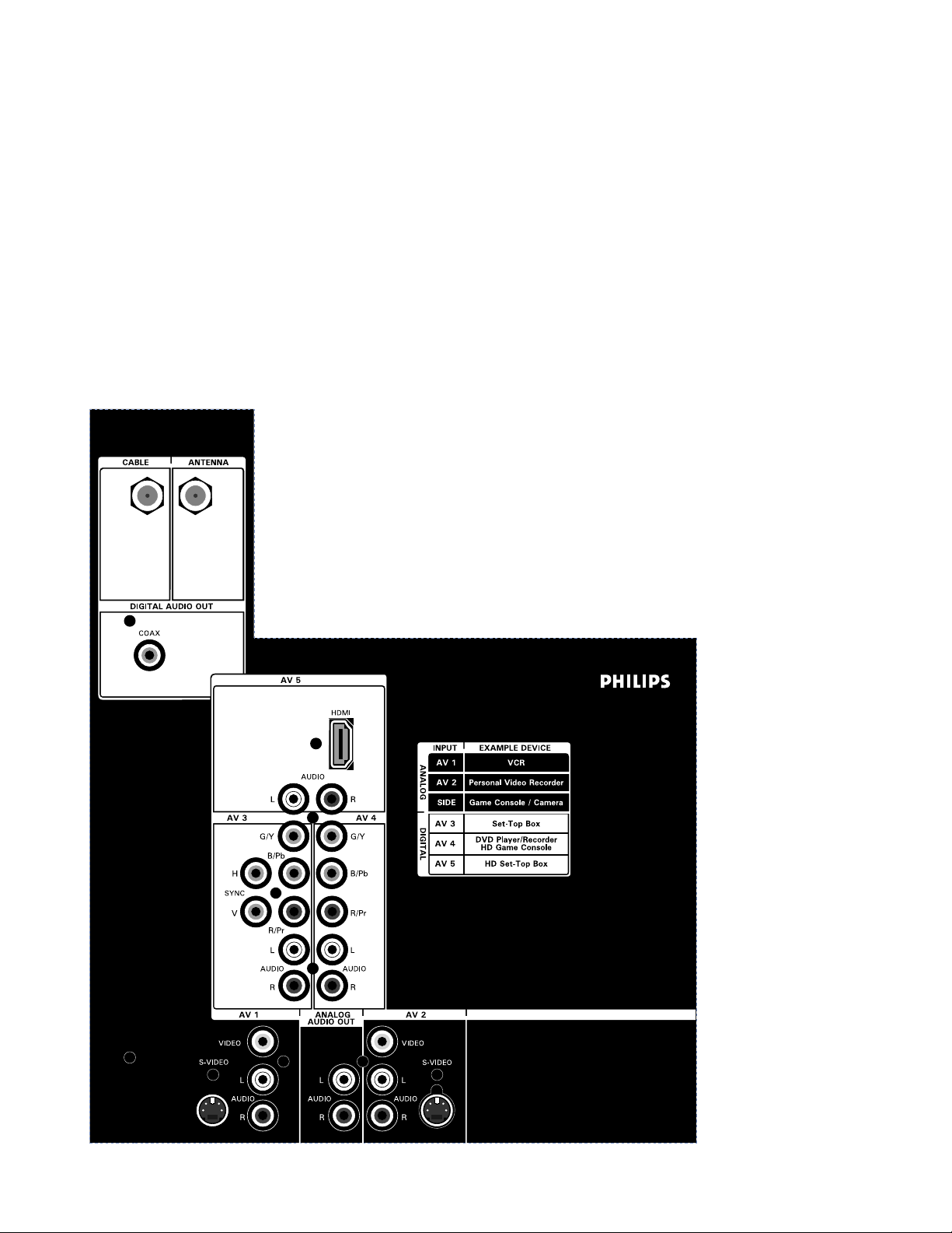
Figure 2 shows the Jack Panel for the HD version. AV1 and AV2 inputs and the Side Jack panel
(not shown) are for the NTSC 1Fh input only. AV3 can accept Component or RGB 1Fh, 480p, 720p,
or 1080i inputs. AV4 can accept Component 1Fh, 480p, 720p, or 1080i inputs. AV5 is a HDMI digital input. This can accept 480p, 720p, or 1080i digital signals.
There are two Antenna inputs, Cable and Antenna. Terrestrial ATSC broadcast signals should be
connected to the Antenna input. This input will decode the 8 VSB signals from ATSC broadcast
stations. The Cable input is designed to decode the QAM signals broadcast by the Cable
companies. Either input will receive NTSC broadcast. If the Cable is connected to the Antenna
input, the set will not receive the QAM HD signals transmitted over the cable. The 8 VSB signal is
an amplitude modulated signal with eight levels representating data bit values. The QAM
(Quadrature Amplitude Modulation) signal combines both amplitude and phase modulation. During
Autoprograming, the set will scan both inputs for signals.
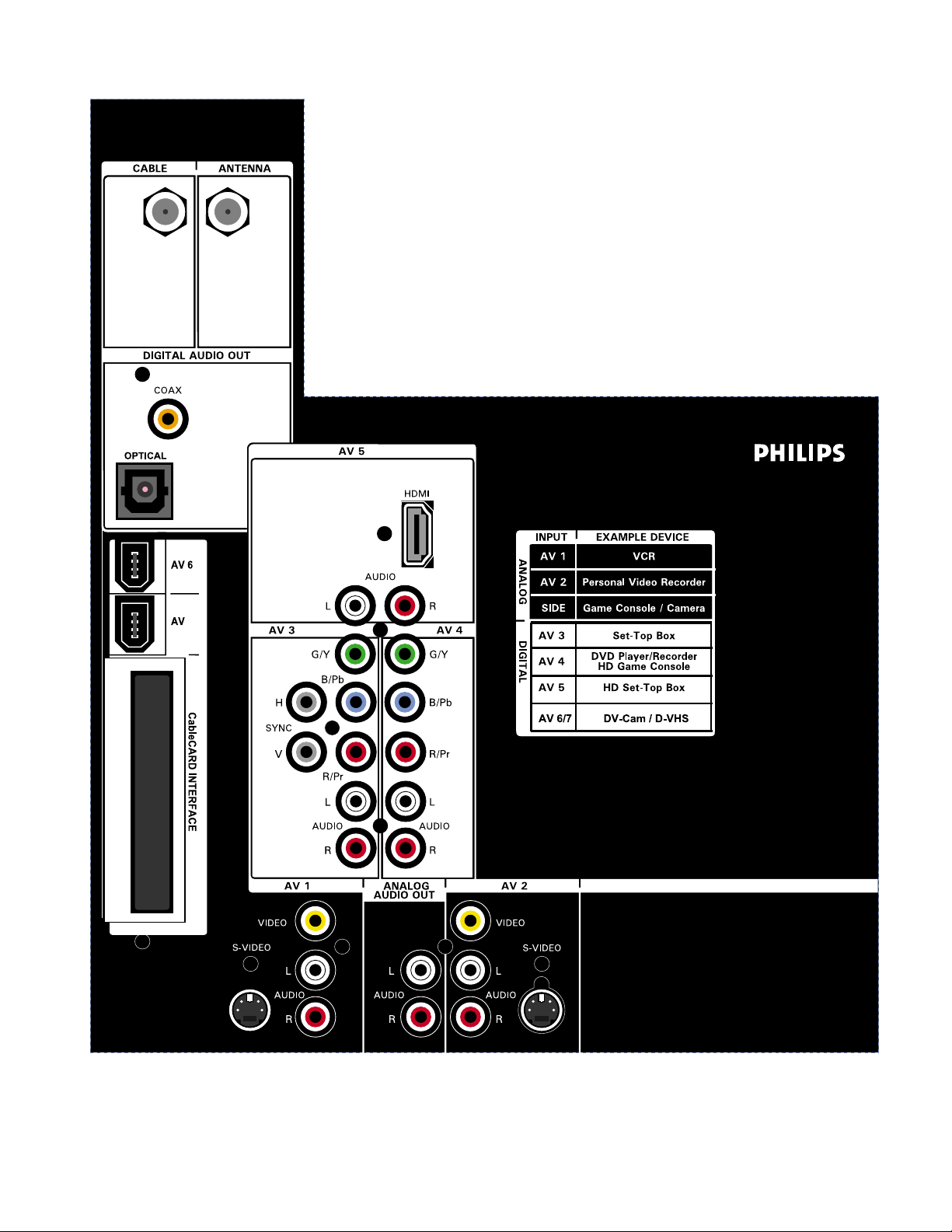
Figure 3 shows the Jack Panel for the Epic version. The inputs are the same as the HD version
except for two additional inputs, AV6 and AV7. These inputs are 1394
Firewire inputs. A digital camera with the 1394 output can be connected to these inputs. A Cable card interface will provide the same function
for interfacing with the cable provider as the Set top box. Optical and
Coax Digital audio output is also available. This is only available for the
ATSC channels.
Page 5
FIGURE 2 - HD REAR JACK PANEL
7
FIGURE 3 - EPIC REAR JACK PANEL
Page 6
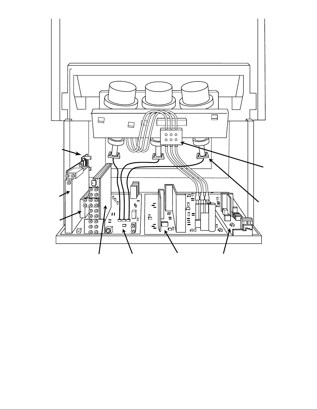
SSB
ATSC
POWER
INTERFACE
PANEL
SSMHD-DW
LSB
AC INPUT
FOCUS
BLOCK
(FG2)
CRT
PANEL
Page 7
BOARD LOCATIONS
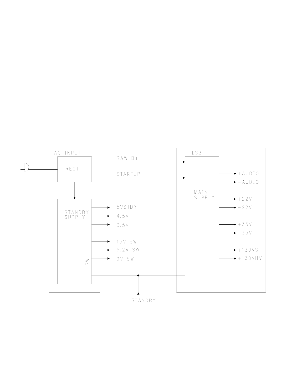
Overall Power Block (Figure 4)
AC power is input to the set via the AC Input panel. The AC Input panel produces the raw DC for
the Main supply located on the LSB (Large Signal Board) and the Standby supply located on the AC
Input panel. When the set is in the Standby mode, the Standby supply produces a +5VSTBY supply.
The standby voltage is fed to the Processor on the SSB (Small Signal Board) via the SSM (Small
Signal Module). When the set is turned On, the Processor on the SSB switches the Standby line
Low. The +15, +5.2, and +9 volt supplies to the SSM are switched On. The +5.2 volt, 3.5-volt, +15
volt, and +4.5-volt supplies to the Power Interface board are also switches On. The Processor on
the SSB also switches the Power Interface supplies On via the Power On/Off control line. The
Power interface board then produces 3.3 volt, 2.5 volt, 12 volt, 1.2 volt, and 5.2 volt supplies to the
ATSC module.
FIGURE 4 - OVERALL POWER BLOCK
Page 8
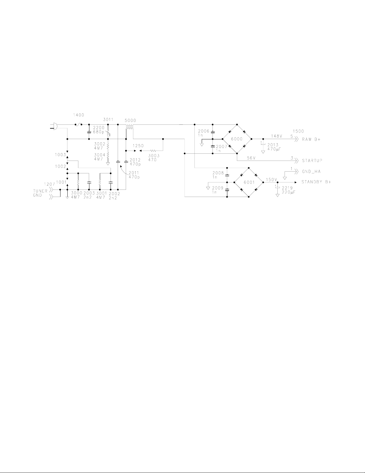
AC Input (Figure 5)
AC power is applied to the to the AC Input panel via connector 1206. A series of spark gaps and
capacitors protect the set from damage due to excessive voltage spikes on the AC line. Filter choke
5000 prevents switch mode noise generated by the set from entering the AC power system, causing
interference with other electrical devices. Bridge 6000 produces RAW DC for the Main power supply located on the LSB. Bridge 6001 produces RAW DC for the Standby supply located on the AC
input panel.
FIGURE 5 - AC INPUT
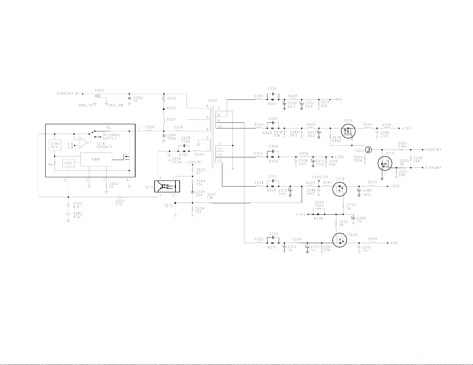
Standby Power Supply (Figure 6)
The Standby supply is located on the AC Input panel. The Standby Supply provides the 5-volt
Standby voltage to the set in the Standby mode. When the set is turned On, it provides +15, +9,
+3.5, +4.5 and +5.2-volt supplies.
Standby B+ is applied to the Standby Switching regulator, 7218 via Pins 6 and 4 of 5202. An internal switch in 7218 charges capacitor 2283 connected to Pin 1 of the IC. When the charge on 2283
reaches 5.8 volts, the internal switch switches to internal. The IC is now being powered by the
charge on capacitor 2283. The internal FET drives transformer 5202 until the charge on capacitor
2283 reaches 4.8 volts. The IC repeats the cycle until the 5-volt Standby voltage reaches the correct level. Shunt regulator 7212 then turns On, turning opto-isolator 7213 On. The operating voltage for 7218 is then supplied by the rectified Hot secondary voltage from Pin 1 of 5202. The internal regulator keeps Pin 1 at 5.8 volts. Regulation is accomplished by monitoring the 5-volt standby
voltage. If the 5-volt supply increases, shunt regulator 7212 will conduct more, causing the resistance of the transistor inside 7218 to decrease. The sensing resistor, Re, inside 7218 will sense the
increase in current and reduce the On time of the internal FET, which will lower the 5-volt supply to
the correct level.
In Standby, the +5 volt, +4.5 volt, and 3.5-volt supplies are being applied to the set. The 3.5 and
4.5-volt supplies are switched on the Power Interface panel. The Standby 5-volt supply is applied to
the Processor located on the SSB. The +15, +9, and +5.2-volt sources are turned Off. When the
set is turned On, the Standby Line goes Low, turning transistor 7214 Off, turning 7205 On, which
turns 7215 On. This switches the +15-volt supply to the set. The +15-volt supply then switches
Page 9

transistors 7216 and 7220 On to switch the +9-volt and +5.2-volt supplies to the set.
When troubleshooting, check for the presence of the operating voltage on Pin 7 of 7218. This is
approximately 160 volts DC. If the Feedback circuit is not working or the secondary is overloaded,
Pin 7 will be pulsing. In this case, check the voltage on Pin 5 of 7213. This is the operating voltage
for Pin 1 of 7218. Each time the 5VSTBY voltage reaches 5 volts, 7212 should turn On. The feedback opto-isolator, 7213 can be checked by applying 5 volts to the +5VSTBY line with AC power
removed from the set. Vary the 5- volt supply between 4 and 6 volts while checking the resistance
between Pins 4 and 5 of 7213. An alternate method of checking this circuit would be to check the
DC voltage on Pins 1 and 2 of 7213. The voltage between these two pins should be 0.7 volts. If
this voltage is present, check Pin 4 of 7213 for a changing voltage. An increase in voltage on this
pin would indicate that 7213 is switching. If the feedback circuit is working, check for an excessive
load on the secondary. If there were no excessive load on the secondary, the cause would be
Capacitor 2283 or IC 7218.
Main Power Supply (Figure 7)
The Full Power supply is located on the Large Signal panel. The Raw B+ voltage from the AC Input
panel is applied to the Full Power switching transistor, 7301 via Pins 6 and 8 of transformer 5300.
This voltage is protected by Fuse 1300 and filtered by Choke 5330. The Standby line goes Low
when the set is turned On. Transistor 7309 is turned Off, which turns 7300 On. This turns Relay
1305 On. Startup voltage is applied to Capacitor 2303 via resistor 3300. When 2303 charges to
14.5 volts, the undervoltage lockout of 7302, connected to Pin 1, is turned On. Drive is output Pin 3
to the Switching FET 7301. This drives 5300 to produce the Full power supply voltages. IC 7302
will continue to drive 5300 until the charges on capacitor 2303 drop below 9.4 volts. The Under
Voltage Lockout of 7302 will then turn the output on Pin 3 Off until 2303 again charges to 14.5 volts.
After several startup cycles, the operating voltage for 7302 is supplied by Pin 10 of 5300.
Regulation is accomplished by monitoring the 130VS supply via resistors 3324, 3350, 3323, and
3322. The Feedback voltage is applied to the Shunt Regulator, 7304, which drives the Feedback
opto-isolator, 7303. The Feedback voltage is applied to Pin 14 of 7302. The voltage is fed to comparator "C" which is referenced to 2.5 volts. This output of this comparator sets the reference voltage for comparator "B" which is compared with the voltage on the source of 7301. This voltage is
developed when 7301 turns On, causing current to flow through resistors 3308 and 3309. If 7301
fails, Resistors 3308 and 3309 should be replaced.
The Full Power supply produces two 130-volt, a 35-volt, a 22-volt, a minus 22-volt, a minus 35-volt,
a plus audio supply, and a minus audio supply. The plus and minus 35-volt, plus 22-volt supplies
power the Convergence circuits located on the SSM. The Audio supply is a plus and minus 19 volts.
This supplies the digital audio amplifier located on the SSM (Small Signal Module).
When troubleshooting, notice that the Hot ground for the Full power supply is separated from the main
Hot ground on the Input Panel by Choke 5330. To ensure correct readings, use the Hot ground in the
Full power supply. If the power supply is overloaded or the operating voltage is missing, the voltage on
Pin 1 of the IC will be changing between 9.4 and 14.5 volts. Each time the voltage reaches 14.5 volts,
drive will appear on Pin 3 of the IC. If the voltage on Pin 1 is rising to 14.5 volts, and drive does not
appear on Pin 3, the IC should be replaced. If a voltage is present on Pin 1 that is greater than 14.5 volts,
and there is no drive on Pin 3, the IC should be replaced. If drive is present on Pin 3, check for drive on
the Drain of 7301. If drive is present here, check for a short on the 130-volt lines, a problem in the feedback circuit, or a problem with the operating voltage.
Page 10
Page 11
FIGURE 6 - STANDBY POWER SUPPLY
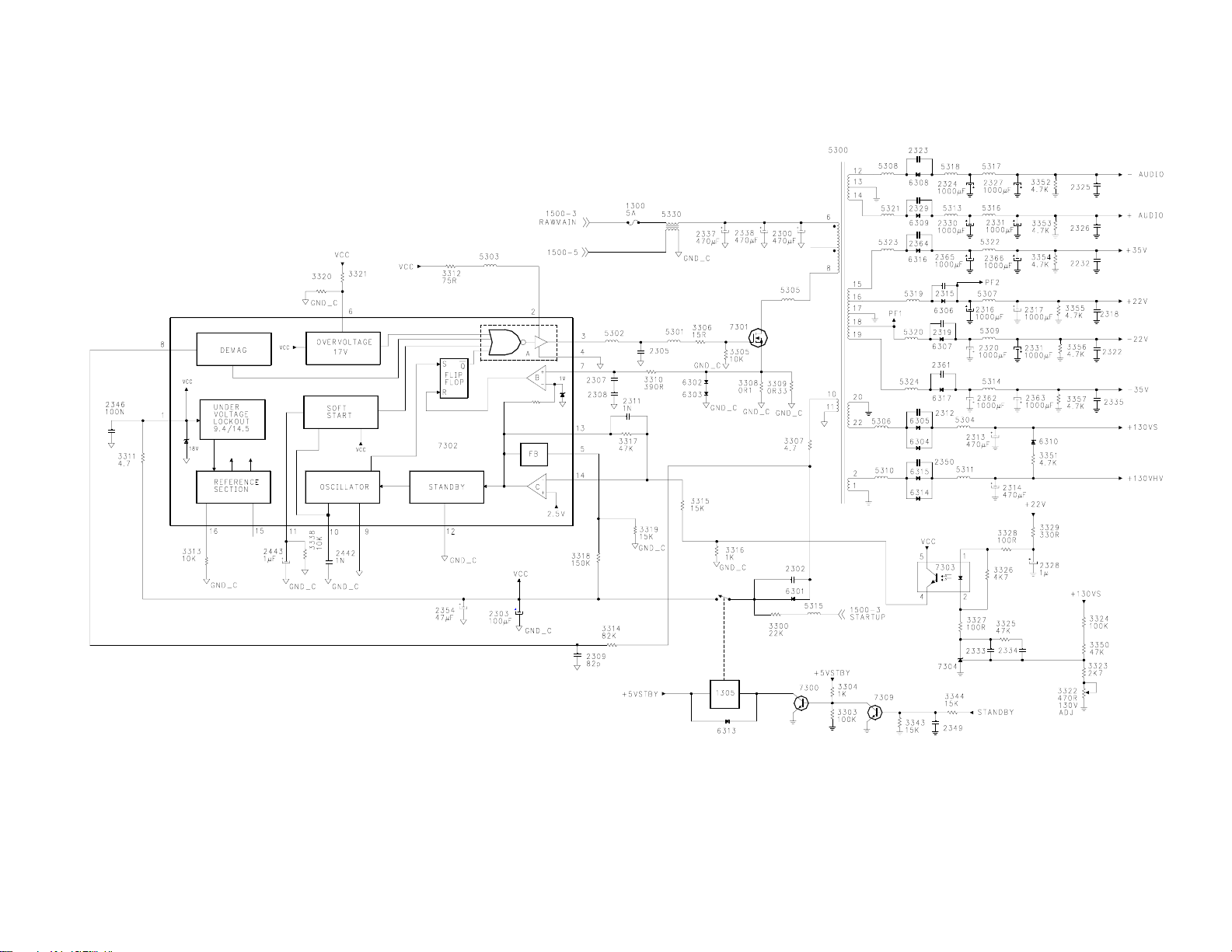
FIGURE 7 - MAIN POWER SUPPLY
Page 12
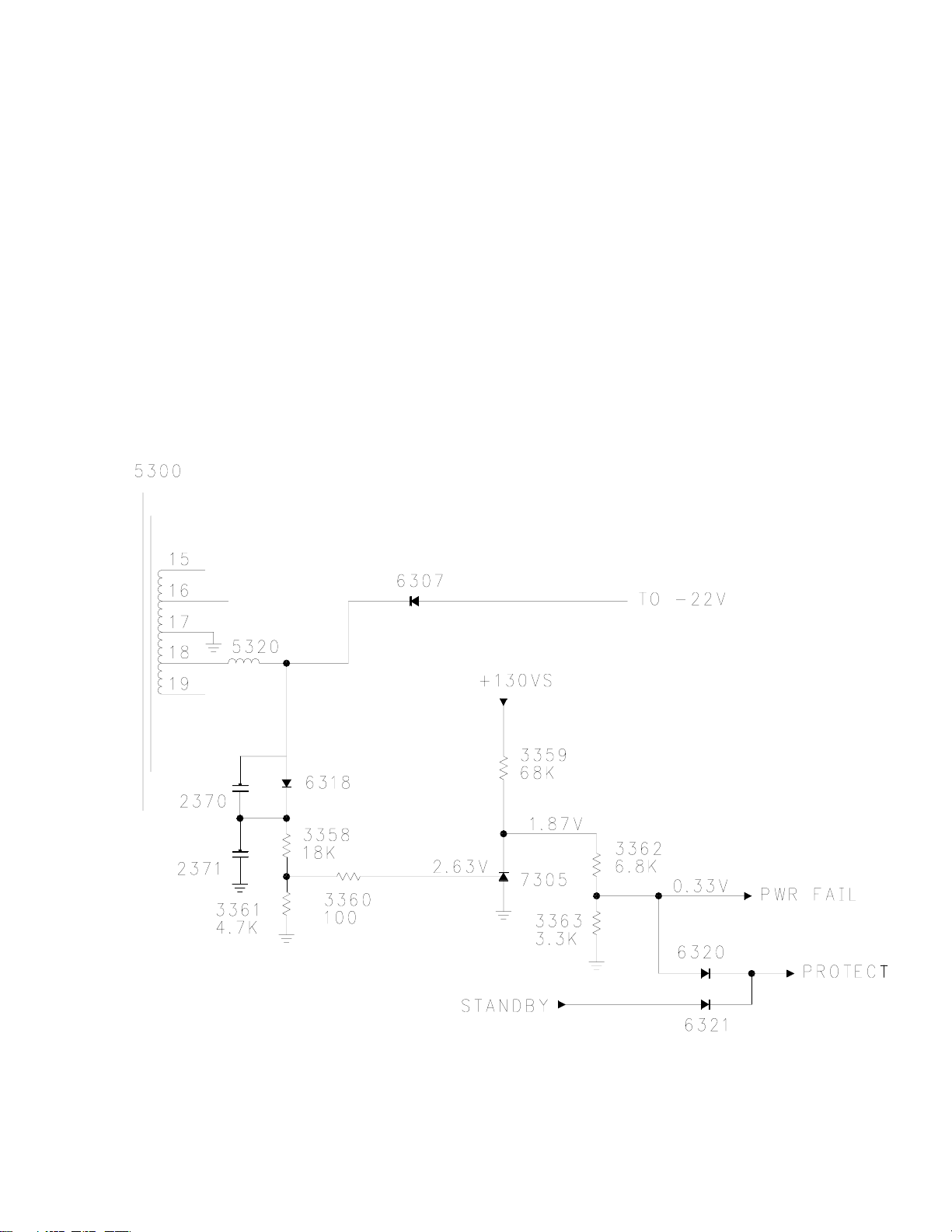
Power Fail detection circuit (Figure 8)
To prevent software problems in the set, the Power Fail detection signals the Processor on the SSB
to place the set in a shutdown state if power is removed while the set is turned On. In addition, the
CRT drive is blanked to prevent phosphor damage to the CRTs.
Voltage from Pin 18 of 5300 is rectified by 6318 and applied to the input of Shunt Regulator 7305.
As long as the voltage to the input of 7305 remains above 2.5 volts, it is turned On. This keeps the
Power Fail and Protect lines Low. If Power is removed from the set, the voltage to the input of 7305
will discharge quickly because of the low capacitance on the input. Shunt Regulator 7305 will then
turn Off. The 130VS supply will then be applied to the Power Fail and Protect lines via resistor
3359. The Power Fail line goes High, signaling the Processor that the set is losing power. When
the Protect line goes High, the CRTs will be blanked and the High Voltage will be turned Off.
Page 13
FIGURE 8 - POWER FAIL DETECTION CIRCUIT
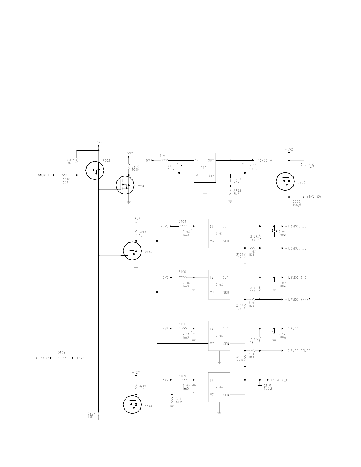
ATSC Power Interface for HD version (Figure 9)
The ATSC Power Interface module produces the operating voltages for the ATSC module. The +15,
3.5, 4.5, and 5.2-volt supplies from the AC Input panel are fed to the Interface module. The
Processor on the SSB provides a On/Off command to switch the outputs. In the Standby mode, the
On/Off line is High. This switches transistor 7202 On, which turns transistors 7206, 7204, and 7205
On. This turns the Regulators 7101, 7102, 7103, 7105, and 7104 Off. When the set is turned On,
the On/Off line goes Low, switching 7202 Off which turns 7206, 7204, and 7205 Off. This turns
Regulators 7101, 7102, 7103, 7105, and 7104 On. The output of 7101 turns transistors 7203 On to
switch the 5.2-volt supply to the ATSC module. A 12-volt, 5.2-volt, two 1.2-volt, 2.5-volt, and 3.3-volt
supplies are fed to the ATSC module. Sense line from the ATSC module for the two 1.2-volt and the
2.5-volt supplies provides precise regulation for those supplies.
FIGURE 9 - ATSC POWER INTERFACE - HD VERSION
Page 14
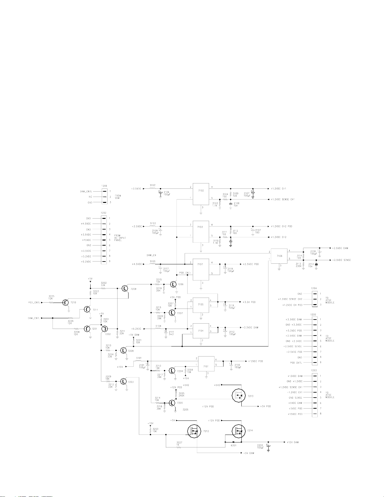
Epic Power Interface (Figure 10)
The ATSC module for the Epic version requires some additional supplies. There are three 1.2, two 3.3,
two 2.5, two 12, and two 5-volt supplies. The DAM_CNTL is switched Low by the microprocessor located
on the SSB when the set is turned On. Transistor 7201 is turned Off which turns 7202 Off. Transistors
7208 and 7203 are switched Off. Transistors 7212 and 7214 turn On to switch the +5V DAM and +12V
DAM supplies On. The DAM_CNTL also turns transistor 7211 On which switches 7209 Off. Transistors
7206, 7207, 7204, and 7205 turn Off. IC 7101 is turned On by the +15-volt supply via resistor 3204. This
switches the +12VDC POD On. The +12VDC POD switches transistor 7213 On, developing the +5V
POD supply. The +5V POD supply then turns IC 7105 On, switching the +3.3V POD supply On. The
+3.3V POD supply switches ICs 7107, 7103, and 7102 On. This switches the +2.5VDC POD, +1.2VDC
CH2 POD, and +1.2VDC CH1 supplies On. The +1.2VDC CH1 supply is fine tuned by feedback from
the ATSC module via the +1.2VDC Sense Ch1 line. The +1.2VDC CH2 POD supply is controlled by the
ATSC module via the +1.2VDC Ch2 feedback. In the same manner, the +2.5VDC DAM supply is controlled by the +2.5VDC Sense from the ATSC module.
The POD_CNTL line from the ATSC module is not used since there is no voltage applied to the ATSC
module in Standby.
Page 15
FIGURE 10 - ATSC POWER INTERFACE - EPIC VERSION

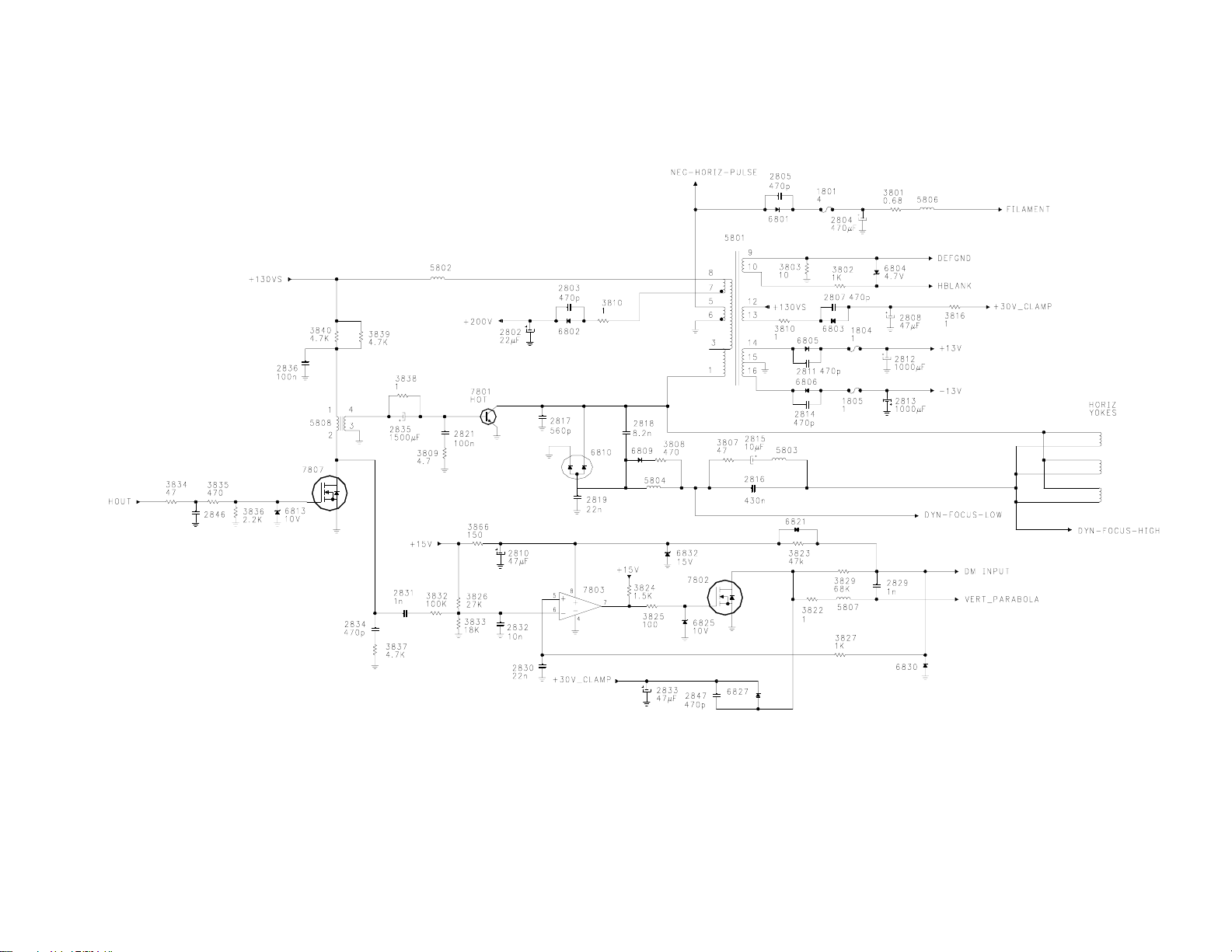
Horizontal Output circuit (Figure 11)
Horizontal drive from the HOP circuit on the SSM is fed to 7807 on the Large Signal panel.
Transistor 7807 drives the Horizontal Output Transistor 7801, which drives the Yokes and the
Horizontal Output Transformer 5801. Transformer 5801 produces a plus and minus 13-volt supply
for the Vertical Output circuit. Voltage from Pin 7 of 5801 is rectified by 6802 to produce the +200volt supply for the CRTs. Voltage from Pin 5 is rectified by 6801 to produce the Filament voltage.
This voltage is filtered by 2804 to provide approximately 6 volts DC. This circuit is protected by fuse
1801 and resistor 3801. The negative Horizontal pulse from Pin 5 feeds the Blanking and Sweep
failure detection circuit.
The output of 7807 drives IC 7803 and transistor 7802. This circuit drives the Dynamic Focus and
Horizontal Geometry correction. The Horizontal component of the correction drives the return side
of the Horizontal yokes via the DYN-FOCUS-HIGH and DYN-FOCUS-LOW lines.
High Voltage and Dynamic drive (Figure 12)
The High Voltage module is an integrated High Voltage supply with its own switching power supply.
When the set is turned On, approximately 10 to 11 volts from the Sweep Failure detection circuit is
fed to diode 6913 and to Pin 8 of the High Voltage module. A supply voltage of 130 volts is also fed
to Pin 10 of the module. The Module then outputs High voltage to the three CRTs. It also outputs
Focus voltage to the Focus G2 block. Output on Pin 4 is rectified by 6917 to produce a negative
200-volt source for the CRT G1 voltage. The voltage is also rectified by 6919 to produce a 330-volt
source for the Dynamic Focus drive. The Dag line along with the output on Pin 2 is connected to
7903 to produce the ABL voltage for the set. If an overcurrent condition should develop with the
drive, the ABL voltage will go Low, turning 7905 On, latching 7904, which will remove drive to Pin 8
of the HVG. This will cause the High voltage to shut Off. The DM-INPUT is mixed with the East
West drive EWO and fed to transistor 7903 which drives 7901. Transistor 7901 drives the Dynamic
Focus and geometry correction drive which is fed to the return side of the Horizontal Yokes via the
DYN-FOCUS-LOW and DYN-FOCUS-HIGH connections.
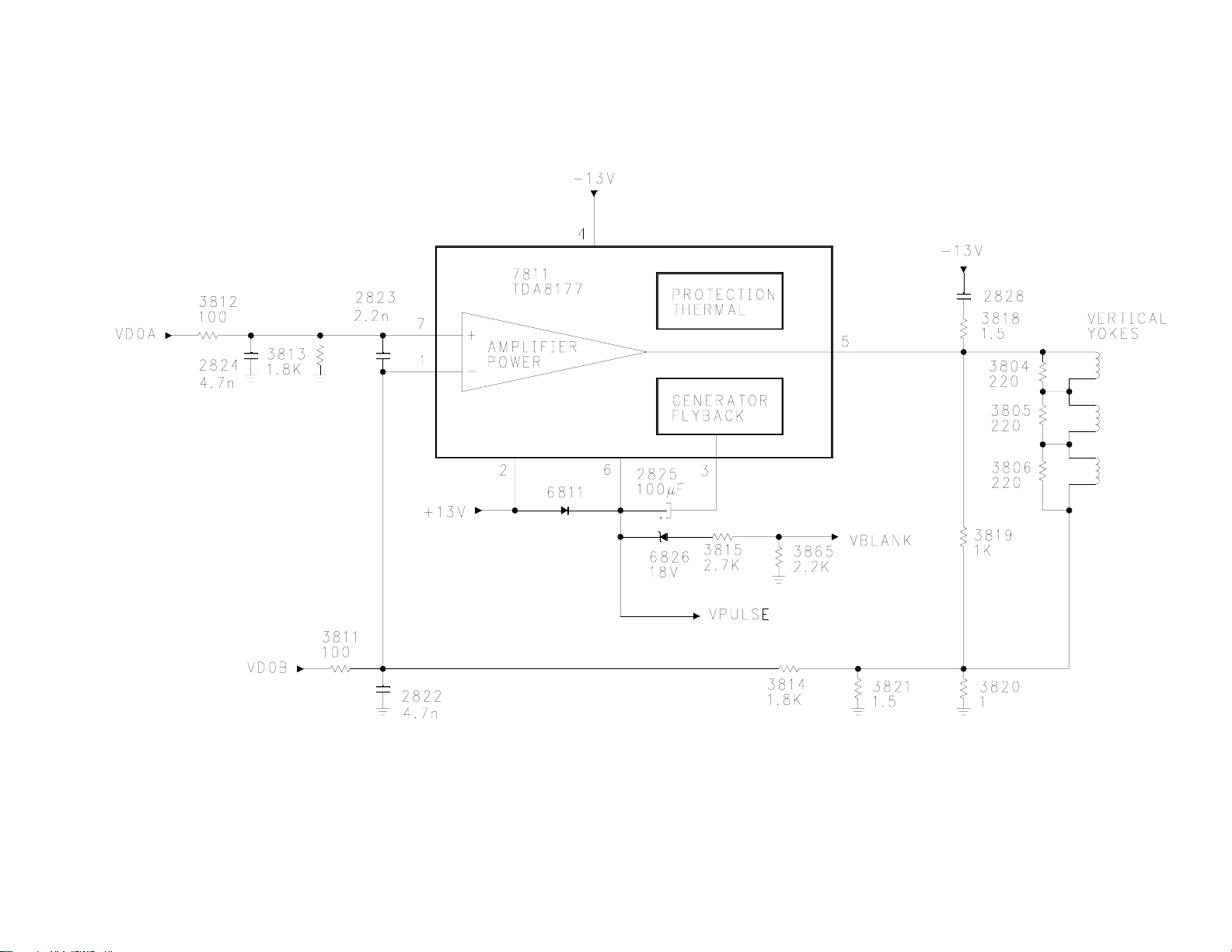
Vertical Amplifier (Figure 13)
The Vertical drive from the HOP panel drives the Vertical Output IC 7811. This IC is located on the
Large Signal panel. Drive is fed to Pin 7 and is output on Pin 5 to drive the three Vertical Yokes.
This IC is powered by the plus and minus 13-volt supplies from the Horizontal Output circuit. A
Vertical pulse on Pin 6 is fed to the sweep failure detection circuit. If there is a failure in the
Horizontal or Vertical sweep, the High Voltage will be shut down.
Page 16
Page 17
FIGURE 11 - HORIZONTAL OUTPUT
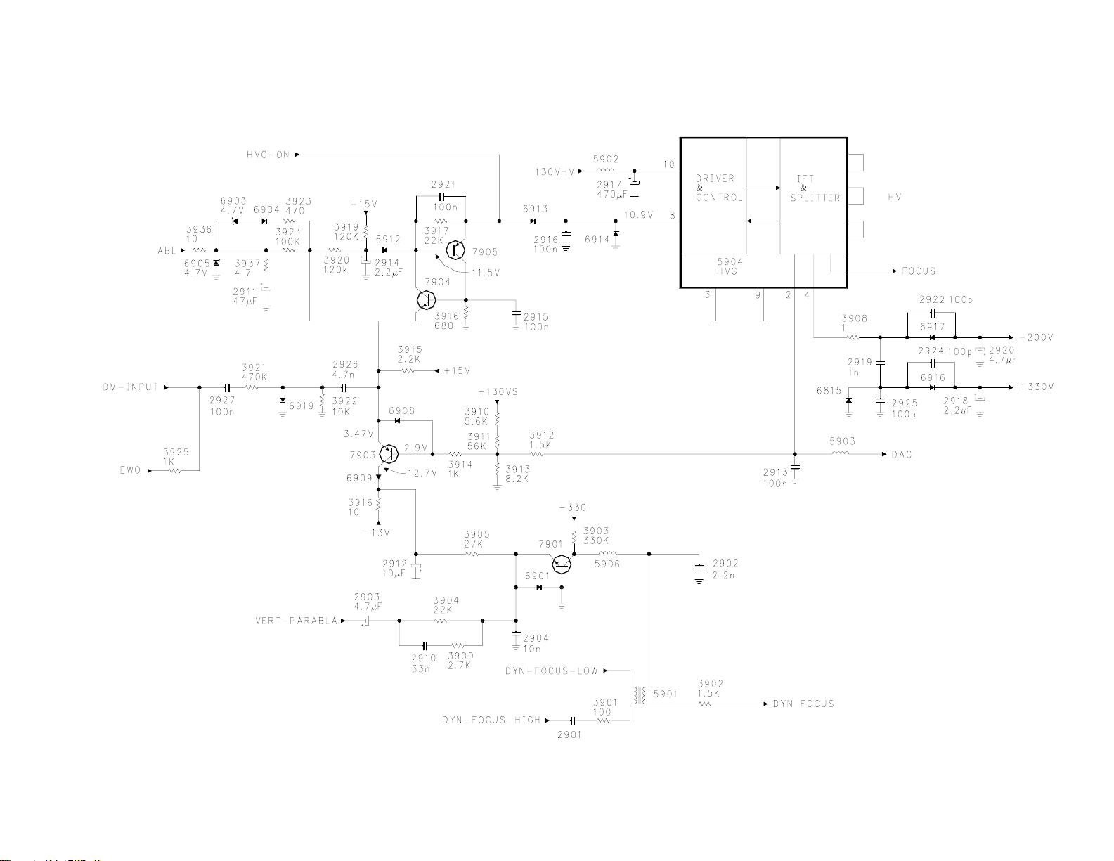
FIGURE 12 - HIGH VOLTAGE
Page 18
Page 19
FIGURE 13 - VERTICAL AMPLIFIER
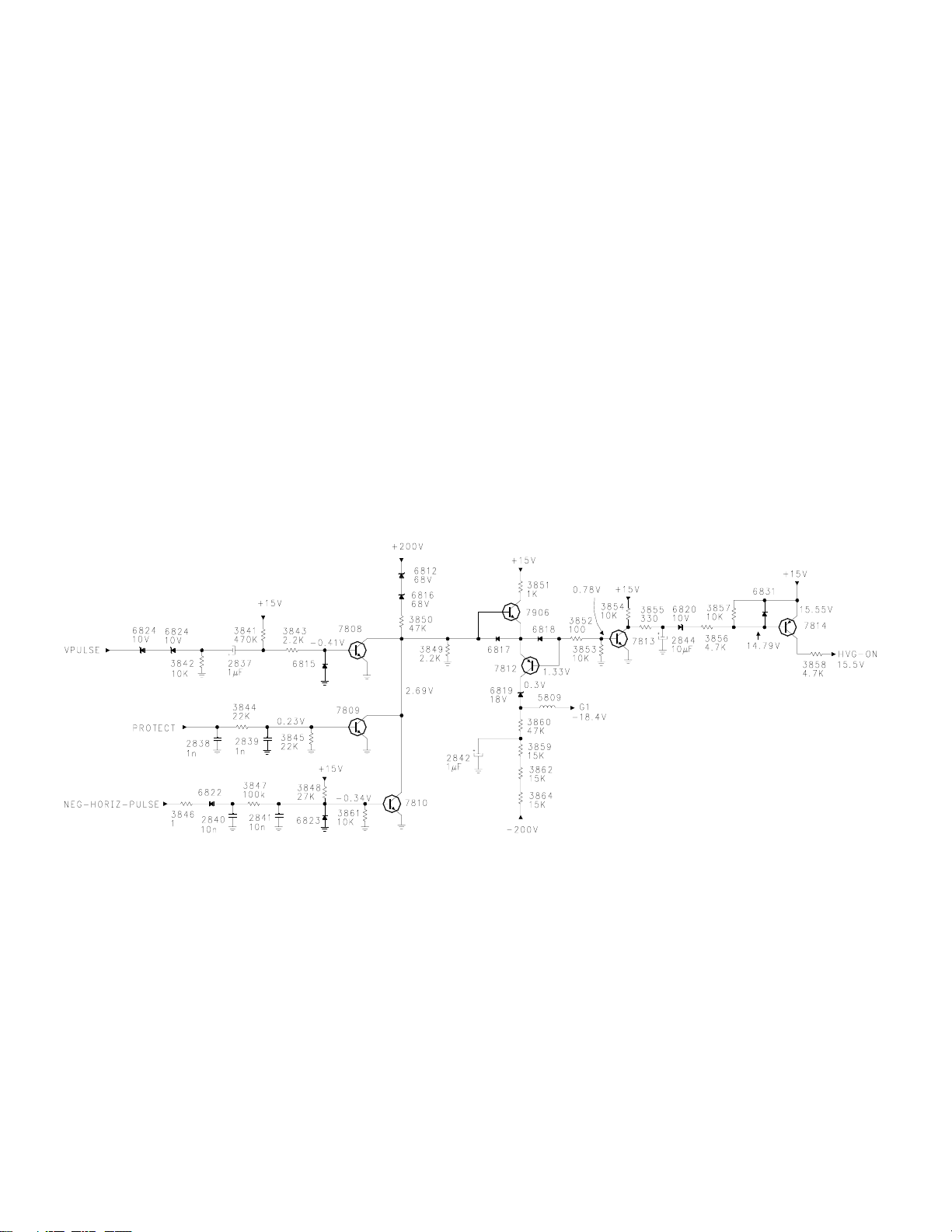
Sweep Failure detection and Blanking (Figure 14)
The Shutdown circuit will shut the High voltage Off if the Horizontal or Vertical Sweep should fail. It will
also shut the High voltage Off if the Power Fail line goes High or the +200-volt source should fail.
The Vertical pulse is fed to zener diodes 6824 and 6814, which keep capacitor 2837 charged. This
pulse is rectified by 6815 to keep the base of 7808 at a negative voltage. This keeps the transistor
turned Off. In the same manner, the Negative Horizontal pulses keep the base of 7810 at a negative voltage to keep it turned Off. The Protect line is normally Low, keeping 7809 turned Off. The
+200-volt source is fed through zener diodes 6812 and 6816, resistor 3850, the base-emitter of
7906, the base emitter of 7812 to keep transistor 7813 turned On. This turns transistor 7814 On,
which switches the On voltage to the High Voltage module. The conduction of 7812 keeps the voltage on the G1 line at approximately -18 volts, which turns the CRTs On. If the Vertical Pulse should
fail, transistor 7808 will turn On, which will turn 7906, 7812, 7813, and 7814 Off. This will turn the
HVG module Off. In addition, when 7812 turns Off, the G1 voltage will go to -200 volts, blanking the
CRTs. The same sequence will occur if Horizontal should fail. The Protect line should go High, or
the +200-volt source should fail.
FIGURE 14 - SWEEP FAILURE DETECTION AND BLANKING Page 20

Video Signal Flow block (Figure 15)
The Tuning system will tune all of the channels in the ATSC, NTSC, and Cable bands. Whichever
channel is selected by the Customer, the video signal is converted to a Digital 8-bit TMDS signal.
This signal is fed to the Scaler IC on the HD/DW panel. Composite or SVHS NTSC signals are fed
to the set via the Side Jack panel, AV1, or AV2. These signals are fed to a Switch located on the
SSM (Small Signal Module). The selected Composite or YC signal is then fed to the HIP circuit on
the SSB where it is changed to a YUV signal. The YUV signal is fed to the HD/DW module for digital processing. The AV3 and AV4 Component signals are fed directly to the HD/DW module. Digital
480p, 720p, or 1080i is fed to the HD/DW module via the HDMI input. The Scaler on the HD/DW
module resizes the picture to 1080i. The 1080i signal is then output to the SSM to the HOP and
CRT drive circuits. OSD (On-Screen Display) generated by the Processor on the SSB is fed to the
HOP to be inserted into the CRT RGB signals. Horizontal and Vertical from the HOP is fed to the
LSB (Large Signal Board) to drive the Scan circuits.
Side Jack Panel (Figure 16)
The Side Jack panel has a Composite Video and SVHS input. When there is a connector in the SVHS
input, the Composite input is muted. Resistors 3001, 3002, and 3000 on the Video, Y, and C lines provide 75-ohm impedance matching. If a cable is plugged into the SVHS connector, the line connecting
resistor 3029 to ground is removed causing the voltage on the Y/C_CVBS_SENSE_FRNT line to
increase. This signals the Microprocessor to switch the video switching circuits from composite video to
YC in.
NTSC AV inputs and switching (Figure 17)
AV1 and AV2 Composite and SVHS inputs are located on the SSM. These inputs as well as the
Side Jack panel are fed to the Video Switch, 7017. This IC is controlled by the Processor on the
SSB via the SCL_IN and SDA_IN bus. Composite video or Luminance is output on Pin 1 and
buffered by 7003 before being fed to the SSB. The Chroma signal is output on Pin 3 and buffered
by 7102. If a SVHS signal is connected to one of the AV inputs, the S-1, S-2, or S-3 lines will go
Low for that respective input. The Processor will read these Pins via the I2C bus and signal the HIP
that the signal present is YC instead of Composite.
Page 21
 Loading...