

Page 1

Colour Television Chassis
DPTV465
AA
E15000_000.eps
191004
Contents Page Contents Page
1 Technical Specifications, Connections,
and Chassis Overview 2
2 Safety Instructions, Warnings, and Notes 4
3 Directions for Use 5
4 Mechanical Instructions 6
5 Service Modes, Error Codes, and Fault Finding 10
6 Block Diagrams, Testpoint Overviews, and
Waveforms
Wiring Diagram 17
2
I
C Overview 18
7 Circuit Diagrams and PWB layouts Diagram PWB
Power Supply Panel: AC Input AP(Diagr. A1) 19 20
SSB: SIM Connector (Male) (Diagram B1) 21 27-29
SSB: IF, I/O Videoprocessing (Diagram B2) 22 27-29
SSB: Feature Box (Diagram B3) 23 27-29
SSB: HOP (Diagram B4) 24 27-29
SSB: Audio Demodulator (Diagram B6) 25 27-29
SSB: Painter (Diagram B7) 26 27-29
Small Signal Module (Diagr. C1-C8) 30-37 42-43
Diversity SSM C1-C8 (Diagr. C9) 38
Mapping SSM, C1-C8 (Diagr. C10-C12) 39-41
CRT Panel: Red (Diagram D(R)1) 44 48
CRT Panel: Green (Diagram D(G)1) 45 48
CRT Panel: Blue (Diagram D(B)1) 46 48
Mapping CRT Panels 47
LSP (Diagram E1-E3) 49-51 54-55
Mapping LSP, E1-E3 52-53
Side Jack Panel (Diagram G1) 56 58
Mapping Side Jack Panel (Diagram G2) 57
ACS Module (Diagram H1-H3) 59-61 63-64
Mapping ACS Module, H1-H3 (Diagram H4) 62
HOP Panel (Diagram J1-J2) 65-66 70
Diversity HOP Panel (Diagram J3) 67
Mapping HOP Panel, J1-J2 (Diagram J4-J5) 68-69
©
Copyright 2004 Philips Consumer Electronics B.V. Eindhoven, The Netherlands.
All rights reserved. No part of this publication may be reproduced, stored in a
retrieval system or transmitted, in any form or by any means, electronic,
mechanical, photocopying, or otherwise without the prior permission of Philips.
Keyboard Panel (Diagram K1) 71 73
Mapping Keyboard Panel (Diagram K2) 72
Mains Switch Panel (Diagram L1) 74 74
Sensor Panel (Diagram M1) 74
8 Alignments 75
9 Circuit Descriptions 81
List of Abbreviations 100
IC Data Sheets 103
10 Spare Parts List 112
11 Revision List 124
Published by JH 472 Service PaCE Printed in the Netherlands Subject to modification EN 3122 785 15001
Page 2
EN 2 DPTV4651.
Technical Specifications, Connections, and Chassis Overview
1. Technical Specifications, Connections, and Chassis Overview
Index of this chapter:
1.1 Technical Specifications
1.2 Connections
1.3 Chassis Overview
1.1 Technical Specifications
1.1.1 Reception
Tuning System : PLL
Nr. Of Presets : 100
Color Systems Off-air : PAL B/G, D/K, I
: SECAM B/G, D/K, K1
: NTSC M, NTSC 4.43
A/V Connections : 480p
: 576p
: 1080i
: NTSC 3.58
: NTSC 4.43
:NTSC Pl.bk.
: PAL B/G Pl.bk.
Sound Systems Off-air : Bi-NICAM BG/D
:2CS B/G, I
: NICAM B/G, D/K, I, L
Frequency Bands : UHF
:VHF
: S-Channels
: Hyperband
Aerial Input : 75 Ohm coax, IEC
type
1.1.2 Picture
Display Type : Rear Projection
: 3 CRTs
Aspect Ratio : 4:3 and 16:9
Picture Screen Diameter : 43” (109 cm)
: 50” (127 cm)
: 55” (140 cm)
1.1.4 Miscellaneous
Ambient Temperature : +5/+45 °C
Mains Voltage : 160 - 276 V_ac (only /
93)
: 90 - 276 V_ac
Mains Frequency : 50/60 Hz
Power Consumptions:
Normal Operation : 180 W avg.
Standby : 0.7 W
Product Dimensions (WxDxH cm):
43 inch model : 106 x 62 x 125
50 inch model : 125 x 71 x 154
55 inch model : 146 x 82 x 151
Product Weight:
43 inch model : 57 kg (176 lbs)
50 inch model : 82 kg (176 lbs)
55 inch model : 85 kg (187 lbs)
1.2 Connections
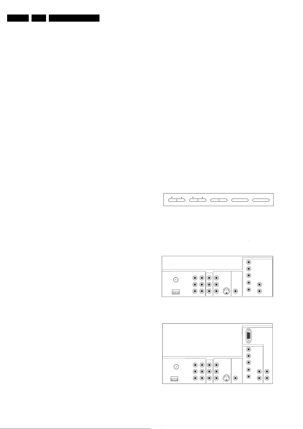
1.2.1 Keyboard 43” and 55”
CHANNELVOLUME MENUSOURCE POWER
Figure 1-1 Keyboard overview
1.2.2 Rear Jack Panel
E_15000_052.eps
141004
Visible Screen Size : 43” (109 cm)
: 50” (127 cm)
: 55” (140 cm)
Picture Enhancements : 100 Hz Dig. Scan (*)
: 120 Hz
: 480p (60 Hz)
: 576p (50 Hz)
: 1152i (50 Hz)
: Progressive Scan
: Interlaced Scan
: Digital Combfilter
: Dynamic Contrast
Color Enhancements : Digital CTI
:Digital Histogram
: Tint Control (3 Modes)
Active Control : Auto Sharpness
: Auto DNR
(*) 100 Hz Digital Scan or Progressive Scan can be switched
with the “On Screen Display" menu.
1.1.3 Sound
Loudspeakers : 2 x 2” Tweeters
: 2 x 5” Woofers
AutoSound™ Control : Theatre, Voice,
Music, Personal
Stereo : Digital NICAM
Sound Output : 2 x 15 W_rms
INPUT-AV 2 SUBWOOFERMONITOR
OUT
Y
AUDIO
VIDEO
L
R
ComPair
VIDEO
AUDIO
INPUT-AV 1ANTENNA IN 75
Pb
L
Pr
R
Figure 1-2 Rear I/O overview 43”
ANTENNA IN 75
ComPair
VIDEO
AUDIO
INPUT-AV 1
L
R
Pb
INPUT-AV 2 SUBWOOFERMONITOR
OUT
Y
Pr
AUDIO
VIDEO
L
R
Figure 1-3 Rear I/O overview 55”
S-VIDEO
S-VIDEO
INPUT AV4-480p/1080i-60Hz, 576p-50Hz
G/Y
R/Pr
B/Pb
V
L
SYNC
AUDIO
H
R
E_15000_053.eps
AV5-RGB, 480p/1080i-60Hz, 576p-50Hz
AV4-480p/1080i-60Hz, 576p-50Hz
G/Y
R/Pr
B/Pb
V
L
SYNC
AUDIO
H
R
E_15000_054.eps
141004
AUDIO
141004
L
R
Page 3

Technical Specifications, Connections, and Chassis Overview
EN 3DPTV465 1.
AV1 (Hosiden: SVHS - In)
1 - Y Ground H
2 - C Ground H
3 - Y 1.0 Vpp / 75 ohm j
4 - C 0.3 Vpp / 75 ohm j
AV1 (Cinch)
Ye - Video (CVBS) 1.0 V_pp / 75 ohm jq
Wh - Audio L 0.5 V_rms / 10 kohm jq
Rd - Audio R 0.5 V_rms / 10 kohm jq
Gn - Y 1.0 V_pp / 75 ohm jq
Bu - Pb 0.7 V_pp / 75 ohm jq
Rd - Pr 0.7 V_pp / 75 ohm jq
Monitor Out (Cinch)
Ye - Video (CVBS) 1.0 V_pp / 75 ohm kq
Wh - Audio L 0.5 V_rms / 10 kohm kq
Rd - Audio R 0.5 V_rms / 10 kohm kq
AV2 (Cinch)
Ye - Video (CVBS) 1.0 V_pp / 75 ohm jq
Wh - Audio L 0.5 V_rms / 10 kohm jq
Rd - Audio R 0.5 V_rms / 10 kohm jq
AV2 (Hosiden: SVHS - In)
1 - Y Ground H
2 - C Ground H
3 - Y 1.0 Vpp / 75 ohm j
4 - C 0.3 Vpp / 75 ohm j
SubWoofer Output (Cinch)
Bk - Variable 0 to 2 V_rms kq
1.2.3 Side Jack Panel 43” and 55”
55”43”
AV3AV3
G
E_15000_055.eps
141004
Figure 1-5 Side I/O overviews
Side I/O (Cinch)
Ye - Video (CVBS) 1.0 V_pp / 75 ohm jq
Wh - Audio L 0.5 V_rms / 10 kohm jq
Rd - Audio R 0.5 V_rms / 10 kohm jq
Side I/O (3.5 mm jack)
Bk - Headphone 10 mW / 8 - 620 ohm t
Side I/O (Hosiden: SVHS - In)
1 - Y Ground H
2 - C Ground H
3 - Y 1.0 Vpp / 75 ohm j
4 - C 0.3 Vpp / 75 ohm j
AV3 - (Cinch)
Gn - G/Y 1.0 V_pp jq
Rd - R/Pr 0.7 V_pp jq
Bu - B/Pb 0.7 V_pp jq
Bk - V-sync 3.0 V_pp / 1 kohm jq
Gy - H-sync 3.0 V_pp / 1 kohm jq
Wh - Audio L 0.5 V_rms / 10 kohm jq
Rd - Audio R 0.5 V_rms / 10 kohm jq
AV4 (Cinch, In)
Wh - Audio L 0.5 V_rms / 10 kohm jq
Rd - Audio R 0.5 V_rms / 10 kohm jq
AV4 (Sub-D 15p, In)
1
6
11
5
10
15
E_06532_002.eps
050404
Figure 1-4 VGA Connector
1 - Red 0.7 V_pp / 75 ohm j
2 - Green 0.7 V_pp / 75 ohm j
3 - Blue 0.7 V_pp / 75 ohm j
4 - Ground H
5-
6 - Ground H
7 - Ground H
8 - Ground H
9-
10 - Ground H
11 - Ground H
12 -
13 - H-sync 0 - 5 V j
14 - V-sync 0 - 5 V j
15 -
1.3 Chassis Overview
CRT
Pane l
PIP
SSB
ACS
SSM
Figure 1-6 PWB location
HOP
LSB
AC INPUT
FOCUS
BLOCK
(FG2)
E_15000_056.eps
141004
Page 4

EN 4 DPTV4652.
Safety Instructions, Warnings, and Notes
2. Safety Instructions, Warnings, and Notes
Index of this chapter:
2.1 Safety Instructions
2.2 Maintenance Instructions
2.3 Warnings
2.4 Notes
2.1 Safety Instructions
Safety regulations require that during a repair:
• Due to the chassis concept, a very large part of the circuitry
(incl. deflection) is 'hot'. Therefore, connect the set to the
mains via an isolation transformer.
• Replace safety components, indicated by the symbol h,
only by components identical to the original ones. Any
other component substitution (other than original type) may
increase risk of fire or electrical shock hazard.
• Wear safety goggles when you replace the CRT.
Safety regulations require that after a repair, you must return
the set in its original condition. Pay, in particular, attention to
the following points:
• General repair instruction: as a strict precaution, we advise
you to re-solder the solder connections through which the
horizontal deflection current is flowing. In particular this is
valid for the:
1. Pins of the line output transformer (LOT).
2. Fly-back capacitor(s).
3. S-correction capacitor(s).
4. Line output transistor.
5. Pins of the connector with wires to the deflection coil.
6. Other components through which the deflection current
flows.
• The maintenance inspection includes the following actions:
1. Perform the 'general repair instruction' noted above.
2. Clean the power supply and deflection circuitry on the
chassis.
3. Clean the picture tube panel and the neck of the picture
tube.
2.3 Warnings
• In order to prevent damage to ICs and transistors, avoid all
high voltage flashovers. In order to prevent damage to the
picture tube, use the method shown in Fig. 2-1, to
discharge the picture tube. Use a high voltage probe and a
multi-meter (position V
reading is 0 V (after approx. 30 s).
V
Figure 2-1 Discharge picture tube
). Discharge until the meter
DC
E_06532_007.eps
250304
Note: This re-soldering is advised to prevent bad connections
due to metal fatigue in solder connections, and is therefore only
necessary for television sets more than two years old.
• Route the wire trees and EHT cable correctly and secure
them with the mounted cable clamps.
• Check the insulation of the mains cord for external
damage.
• Check the strain relief of the mains cord for proper function,
to prevent the cord from touching the CRT, hot
components, or heat sinks.
• Check the electrical DC resistance between the mains plug
and the secondary side (only for sets that have an isolated
power supply). Do this as follows:
1. Unplug the mains cord and connect a wire between the
two pins of the mains plug.
2. Turn on the main power switch (keep the mains cord
unplugged!).
3. Measure the resistance value between the pins of the
mains plug and the metal shielding of the tuner or the
aerial connection of the set. The reading should be
between 4.5 MΩ and 12 MΩ.
4. Switch the TV 'off' and remove the wire between the
two pins of the mains plug.
• Check the cabinet for defects, to prevent the possibility of
the customer touching any internal parts.
2.2 Maintenance Instructions
• All ICs and many other semiconductors are susceptible to
electrostatic discharges (ESD, w). Careless handling
during repair can reduce life drastically. Make sure that,
during repair, you are connected with the same potential as
the mass of the set by a wristband with resistance. Keep
components and tools also at this potential. Available ESD
protection equipment:
– Complete kit ESD3 (small tablemat, wristband,
connection box, extension cable and ground cable)
4822 310 10671.
– Wristband tester 4822 344 13999.
• Together with the deflection unit and any multi-pole unit,
flat square picture tubes form an integrated unit. The
deflection and the multi-pole units are set optimally at the
factory. We do not recommend adjusting this unit during
repair.
• Be careful during measurements in the high voltage
section and on the picture tube.
• Never replace modules or other components while the unit
is 'on’.
• When you align the set, use plastic rather than metal tools.
This will prevent any short circuits and the danger of a
circuit becoming unstable.
2.4 Notes
2.4.1 General
We recommend a maintenance inspection carried out by
qualified service personnel. The interval depends on the usage
conditions:
• When a customer uses the set under normal
circumstances, for example in a living room, the
recommended interval is three to five years.
• When a customer uses the set in an environment with
higher dust, grease, or moisture levels, for example in a
kitchen, the recommended interval is one year.
• Measure the voltages and waveforms with regard to the
chassis (= tuner) ground (H), or hot ground (I), depending
on the tested area of circuitry.
• The voltages and waveforms shown in the diagrams are
indicative. Measure them in the Service Default Mode (see
chapter 5) with a colour bar signal and stereo sound (L: 3
kHz, R: 1 kHz unless stated otherwise) and picture carrier
at 475.25 MHz (PAL) or 61.25 MHz (NTSC, channel 3).
Page 5

Directions for Use
EN 5DPTV465 3.
• Where necessary, measure the waveforms and voltages
with (D) and without (E) aerial signal. Measure the
voltages in the power supply section both in normal
operation (G) and in standby (F). These values are
indicated by means of the appropriate symbols.
• The picture tube panel has printed spark gaps. Each spark
gap is connected between an electrode of the picture tube
and the Aquadag coating.
• The semiconductors indicated in the circuit diagram and in
the parts lists, are interchangeable per position with the
semiconductors in the unit, irrespective of the type
indication on these semiconductors.
3. Directions for Use
You can download this information from the following websites:
http://www.philips.com/support
http://www.p4c.philips.com
• Manufactured under license from Dolby Laboratories.
‘Dolby’, ‘Pro Logic’ and the ‘double-D symbol’, are
trademarks of Dolby Laboratories.
E_06532_006.eps
240604
Figure 2-2 Dolby PL Symbol
Page 6

EN 6 DPTV4654.
PHILIPS
Mechanical Instructions
4. Mechanical Instructions
Index of this chapter:
4.1 Disassembly Procedures
4.2 Service Position
4.3 Picture Tube Replacement
4.4 Set Re-assembly
Notes:
• Figures below can deviate slightly from the actual situation,
due to the different set executions.
• Follow the disassembly instructions in described order.
AC21
AC34
AC22
AC23
AC21
AC10
(bracket)
AC27
F
AC26
AC09
AC33
Remote
AC31
AC13
AC16
AC05
i
AC15
G
AC14
H
AC22
DFU
(Owner's Manual)
AC11
E
4.1 Disassembly Procedures
All numbers, found in the following text, refer to the drawing
below and apply to both the 43” and 55” models.
Note:
• Not all shown items are available for all models.
• If you are servicing a PWB or speaker, you do not need to
remove the plastic Upper Back Cover (4).
43" CABINET EXPLODED VIEW
AC22
C
AC20
AC12
AC32
AC07
D
C
AC17
(mirror)
AC12
C
AC02
D
AC06
(chassis frame)
AC20
A
AC19
AC11
AC01
B
AC26
A
AC08
I
A
AC03
AC04
AC31
(Module Bracket)
(Support)
3135 034 00361
AC28
DFU
(Owner's Manual)
REMOTE
1186
POWER
ACC
TV
VCR
ACTIVE
CONTROL
SWAP PIP CH
FREEZE
DN
UP
PICTURE
SOUND
MENU/
STATUS/
SELECT
EXIT
MUTE
CH
VOL
213
546
879
TV/VCR
A/CH
SURF
0
PIP
POSITION
Optical Assembly
G
EEH
E_15000_057.eps
141004
Figure 4-1 Exploded view 43” cabinet
165
TYPICAL 46"/50"/55" CABINET EXPLODED VIEW
NOTE: NOT ALL ITEMS SHOWN ARE AVAILABLE FOR ALL MODELS.
J
34
46
79
1035
80
95
117
44
77
!
8190
154
(caster)
88
115
31
Located under
top of cabinet
26
9
57
5208
5206
59
37
A
PHILIPS
......................................................................................................................................
......................................................................................................................................
......................................................................................................................................
......................................................................................................................................
......................................................................................................................................
......................................................................................................................................
....................................................................................................................................
....................................................................................................................................
....................................................................................................................................
...................................................................................................................................
...................................................................................................................................
..................................................................................................................................
..................................................................................................................................
.................................................................................................................................
.................................................................................................................................
................................................................................................................................
................................................................................................................................
...............................................................................................................................
...............................................................................................................................
...............................................................................................................................
..............................................................................................................................
..............................................................................................................................
..............................................................................................................................
.............................................................................................................................
.............................................................................................................................
.............................................................................................................................
.............................................................................................................................
.............................................................................................................................
.............................................................................................................................
.............................................................................................................................
.............................................................................................................................
.............................................................................................................................
.............................................................................................................................
..............................................................................................................................
..............................................................................................................................
..............................................................................................................................
..............................................................................................................................
..............................................................................................................................
..............................................................................................................................
..............................................................................................................................
5
Right
Left
B
F
F
75
G
76
68
C
C
86
A
2
–
Intelli
+
Sense
4527
B
E_15000_058.eps
35
36
66
4
141004
Figure 4-2 Exploded view 55” cabinet
Page 7

Mechanical Instructions
EN 7DPTV465 4.
4.1.1 Lower Center Back Cover Removal (86)
1. Remove all screws (B and C).
2. Remove the Lower Center Back Cover.
4.1.2 Side Back Cover Removal
Remove all screws (F) from each of the Side Back Covers
(some prying may be necessary to dislodge covers).
Note: This allows access to the Side Jack Panel and to the Left
and the Right Speakers.
4.1.3 Large Signal Board Removal (LSB)
Note: See for the location of the panels figure "PWB location"
in Chapter 1 "Technical Specifications, Connection Facilities,
and Chassis Overview".
1. Disconnect all cables.
2. Remove three screws from the center of the PWB and pull
three tabs on the right of the bracket.
3. Lift the right side of the LSB and slide the panel up and out.
4.1.4 AC Input Panel Removal
1. Disconnect all cables.
2. Remove four screws from the PWB.
3. Lift the AC Input Panel up and out.
4.1.5 Small Signal Module Removal (SSM)
1. Remove three screws along the rear of the chassis frame.
2. Remove two screws, which hold the chassis frame and are
located between the LSB and SSB panels.
3. Remove one screw, which holds the chassis frame and is
located between the Input Power and LSB panels
4. Remove the rear Jack Panel cover (76).
5. Slide the Chassis assembly rearward to allow access to the
Module Bracket.
6. Remove the screws, which secure the Module Bracket,
and release the cables.
7. Remove two screws from the centre of the SSM PWB.
8. Pull three tabs on the right of the panel bracket.
9. Lift the right side of the SSM, then move the SSM to the
right to remove it.
4.1.6 Side Jack Panel Removal
1. Carefully pull the ACS panel upward to separate it from the
SSM connectors.
2. Disconnect the cable assemblies.
4.1.10 Wide Band Video Panel Removal (HOP)
First, remove the Module Bracket (see the chapter “Small
Signal Module Removal”).
1. Remove the rear Jack Panel cover (76).
2. Disconnect the ribbon cable connectors.
3. Carefully separate the HOP panel from the SSM
connectors.
4.1.11 Front Control Panel and Left or Right Speaker Removal (5)
1. Remove the Left and Right Side Back Covers.
2. Remove the two screws (on either side) of the speaker
location.
3. Release two tabs on either side of the speaker baffle and
pull the baffle forwards.
4. Loosen the ribbon cable and the grounding wire to allow
working space.
5. Remove two screws to remove the Front Control Panel
(4527).
6. Remove four screws each to remove the speakers (5208/
5206).
4.1.12 Upper Back Cover Removal (4)
1. Remove all screws (A and B).
2. Lift the cover up to dislodge from pegs (J) and remove the
cover.
4.1.13 Plastic Light Barrier Removal (Optical Assembly)
Remove two screws (E) (one each at either end of the plastic
light barrier).
4.1.14 Mirror Mounting Board Removal (57)
Remove all screws, located in the mirror mounting board
brackets, and remove the board.
Note: Take care not to place fingerprints or smudges on the
mirror.
4.1.15 Complete Optical Assembly or Individual CRT Assembly Removal
1. Remove the Left Side Back Cover (see procedure above
excluding the Module Bracket removal).
2. Remove two screws from the panel.
3. Slide the Side Jack Panel PWB out of the bracket.
4.1.7 PIP Panel Removal (if present)
1. Remove the rear Jack Panel cover (76).
2. Remove three screws from the PIP panel.
4.1.8 Small Signal Board Removal (SSB)
First, remove the Module Bracket (see the chapter “Small
Signal Module Removal”).
1. Release the metal retainer clips, located at the front and
rear edges of the SIMM connector.
2. Tilt the SSB to the right and then pull it up.
4.1.9 Convergence Panel Removal (ACS)
First, remove the Module Bracket (see the chapter “Small
Signal Module Removal”).
1. Remove the Plastic Light Barrier.
2. Disconnect the CRT panels, 2nd anode leads (at HVT),
and the yoke connectors from assemblies to be removed.
3. To remove the complete Optical Assembly, remove four
screws (G) and lift the assembly up and out.
4. To remove individual CRT assemblies, remove four screws
(H) from the desired assembly and lift the assembly up and
out.
Caution: Do not disturb the focus assembly wing nuts, as this
will misadjust mechanical focus.
Page 8

EN 8 DPTV4654.
Mechanical Instructions
4.2 Service Position
1. Remove the Side Back Covers.
2. Remove the Front Speaker Baffle.
3. Remove the Front Control Panel.
4. Route the ribbon cable and the wire through opening and
into the back of the unit.
5. Reconnect the ribbon cable to the Front Control Panel.
6. Remove the Side Jack Panel to allow room for cable
movement.
7. Remove the rear Jack Panel cover (76).
8. Being careful with the PIP Panel, pull the Chassis Frame
out and tilt up.
9. Place the Chassis Frame on the bottom board of the PTV.
4.3 Picture Tube Replacement
Replacement of the cathode ray tube (CRT) and/or optical
system components of a Projection TV (PTV) can be easily
accomplished by following general guidelines. Use care when
working around the CRT and optical systems of the PTV. The
PTV light path encompasses a number of precision optical
components. These include lenses, mirrors, the lenticular
screen, and Fresnel lens. The PTV incorporates three separate
CRTs, representing green, red, and blue outputs. Each CRT
uses an independent deflection/convergence yoke, magnetic
centring ring, coupler, C-element lens, and output lens (A/B
lens). Each tube is mechanically fastened to a coupler which
houses fluid (a glycol-type substance) used to cool the high
temperatures generated by the small (7") CRTs. The fluid also
provides an optical characteristic supporting the optical system
of the PTV. When replacement of a CRT or optical component
is required, caution must be exercised in preventing fluid
spillage. The technician must carefully reassemble the CRT/
optical components, ensuring a proper seal of the coupling
fluid. Use only factory original coupling fluid.
Caution: Do not use or add water as an alternative to the
prescribed coupling fluid.
Note: Upon completion of CRT/optical assembly repair, the
centring, convergence, grey scale, mechanical and electrical
focus adjustments are required. If more than one assembly
requires repair, it is recommended the service technician fully
complete one assembly at a time, using the existing
assemblies as a reference for the alignment of the centring and
convergence.
The following procedure should be used when performing
repairs on the CRT/optical assemblies of the Projection TV.
4.3.1 Disassembly Procedure
A. Removal of a single CRT/Lens Assembly from the light rack
1. Remove AC power from the PTV.
2. Remove the upper and lower back covers (1/4" screws).
3. Remove the barrier board and the shield cover from around
the lens assemblies (1/4" screws).
4. Carefully remove the CRT Socket Board from the CRT of
the CRT/optical assembly being serviced.
5. Remove the yoke and convergence plugs, of the CRT/
optical assembly being serviced, from the Large Signal
Module.
6. Remove the high voltage anode lead from the HV splitter
block on the Large Signal Module of the CRT/optical
assembly being serviced. Remove ground lug connectors
from the coupler frame.
7. Remove the four 1/4" screws that secure the CRT/lens
assembly to the light rack. These four screws are located
in each corner, on the top of the coupler assembly.
Caution: Do not remove the bolts with pressure springs or
the inverted Torx screws of the CRT/lens assembly. The
removal of these components could result in fluid spillage
into the PTV cabinet.
8. Carefully remove the CRT/Lens assembly from the PTV
cabinet.
4.3.2 Servicing the CRT/Lens Assembly
Warning: Coupling fluid is a poisonous solution containing a
high concentration of ethylene glycol. Do not leave exposed
fluid unattended. Prevent children or pets from coming into
contact with the fluid. Clean up spills immediately.
Caution: Do not attempt any repairs on the CRT/optical block
assembly without first removing the CRT coupling fluid.
Removal of the delta output lens will result in spillage of the
coupling fluid.
B. Removing the PTV Coupling Fluid
All repairs made to the CRT/optical block assembly require the
removal of the coupling fluid. The following procedure
describes how to remove the PTV coupling fluid.
1. Lay the CRT assembly on its side with the plug pointing up.
2. Remove the plug (X8).
3. Remove some of the fluid from the coupler to prevent
spillage when the CRT is removed. An empty coupling fluid
bottle with a cone top is recommended to lower the fluid
level within the coupler. Squeeze and hold the bottle and
insert the tip of the cap into the drain hole of the coupler.
Loosen the grip on the bottle, allowing the fluid to be pulled
up into the bottle. Save the fluid.
4. Reinstall the plug (X8).
5. Stand the CRT assembly up with the neck of the CRT
pointing up.
6. With an awl or marking pen, outline the edges of the CRT
onto the coupler.
Note: The correct positioning of the CRT to the coupler is
critical to the optimum performance of the optical system.
7. Remove the four CRT mounting bolts (A) (with springs and
spacers) and remove the mounting bracket (D).
8. Remove the four CRT mounting ear screws.
Note: The CRT mounting ear screws are not used on some
assemblies.
9. Gently remove any metal shavings from around the screw
holes. Do not allow the metal shavings to get into the fluid.
Note the position of the high voltage anode cap with
respect to the coupler.
10. Carefully remove the CRT from the coupler. Wipe any
excess fluid from the faceplate of the CRT. Set the CRT
aside.
11. Use an empty coupling fluid bottle to extract the remainder
of the fluid from the coupler.
Note: Complete removal of the coupling fluid is not
necessary when only replacing the CRT.
12. Clean any remaining fluid from the coupler and the CRT
gasket channel using absorbent tissue. Refer to "C".
Cleaning the Coupler, C-element Lens, and CRT
Faceplate procedure if the fluid is discoloured or
contaminated.
13. Make all necessary repairs.
C. Cleaning the Coupler, C-Element Lens, and CRT Faceplate
1. Remove CRT coupling fluid as described in steps B1
through B13.
2. Using denatured alcohol on a cloth made of 100% cotton
or a lens cleaning tissue, gently clean the C-element
(fisheye) lens, coupler and the CRT faceplate. Thoroughly
clean the coupler assembly, including the expansion
chamber bladder, and allow to fully dry.
Caution: Do not use soap or detergent type substances to
clean the coupler and its related assemblies. Water can be
used as an alternative to denatured alcohol, but the
assemblies must be completely dry before reassembly of
the coupler and the addition of the coupling fluid. A hair
Page 9

Mechanical Instructions
EN 9DPTV465 4.
dryer may be used to dry the coupler and its assemblies
before reassembly. If contaminated fluid is discovered, the
coupler and its related assemblies must be completely
disassembled and cleaned to prevent a reoccurrence.
3. Replace the CRT and C-element lens gaskets.
4. Reassemble the C-element lens and the output lens to the
coupler.
5. Refer to "Replacing the CRT Coupling Fluid" upon
completion of necessary repairs and cleaning of the
optical/coupler assemblies.
D. Replacement of the CRT
1. Remove CRT coupling fluid as described in steps B1
through B13.
2. Remove the plastic protective coating (if present) from the
faceplate of the replacement CRT.
3. Refer to "Replacing the CRT Coupling Fluid" to complete
the CRT replacement.
E. Repair or Replacement of the Optical/Coupler Assembly
1. Remove CRT coupling fluid as described in steps B1
through B13.
2. Remove the four inverted-type Torx screws, which secure
the Delta output lens to the coupler. An inverted-type Torx
socket can be purchased using part number 4835 395
17303.
3. Removal of the Delta output lens will allow access to the Celement lens, C-element gasket, coupler, and its
assemblies.
4. Refer to "Replacing the CRT Coupling Fluid" upon
completion of necessary repairs to the optical/coupler
assemblies.
the top of the coupler at the plug. Wipe any excess fluid
from around the coupler.
11. Reinstall the plug and check for any fluid leaks.
12. Install the repaired CRT/optical block assembly into the
PTV and perform any necessary adjustments.
4.4 Set Re-assembly
To re-assemble the whole set, execute all processes in reverse
order.
Note: While re-assembling, make sure that all cables are
placed and connected in their original position
F. Replacing the PTV Coupling Fluid
Notes:
• Before replacing the CRT coupling fluid, ensure the
expansion chamber bladder is fully collapsed. This can be
easily inspected by viewing the bladder through the small
hole on the expansion chamber assembly. If the rubber of
the bladder is not easily visible through the small hole, then
the bladder may be considered collapsed and fluid can be
added. If the rubber of the expansion chamber bladder is
visible at the hole of the expansion chamber, then
replacement of the expansion chamber bladder is required.
• The CRT coupling fluid is critical to the optical performance
of the PTV. Use only part number 4835 310 67032 (3 bottle
kit) or 4835 310 67031 (1 bottle) to ensure the optical
integrity and performance reliability of the PTV when
replacing the CRT coupling fluid.
1. Reinstall the CRT gasket into the gasket channel of the
coupler. Confirm the placement of the CRT, C-element
lens, and vent plug gaskets.
2. Place the CRT onto the coupler with the high voltage
anode lead positioned as marked in step 10 of procedure
B.
3. Carefully position the CRT onto the coupler, using the
outline defined in step 6 of procedure B as a reference.
4. Start the CRT mounting ear screws but do not tighten
them.
5. Tighten the CRT mounting ear screws in a star pattern (like
tightening lug nuts on the wheel of a car). Make sure the
CRT does not shift position from the outline defined in step
B6.
Caution: do not over tighten the CRT ear screws (the CRT
mounting ear screws are not used on some assemblies).
6. Install the CRT mounting bracket and start the four CRT
mounting bracket bolts with springs.
7. Tighten the bolts in a star pattern.
8. Lay the CRT assembly on its side with the plug pointing up.
9. Remove the plug.
10. Using the PTV coupling fluid bottle with the cone top, refill
the coupler with fluid through the drain access hole.
Completely fill the coupler chamber so the fluid is level with
Page 10

EN 10 DPTV4655.
Service Modes, Error Codes, and Fault Finding
5. Service Modes, Error Codes, and Fault Finding
Index of this chapter:
5.1 Test Conditions
5.2 Service Modes
5.3 Problems and Solving Tips (related to CSM)
5.4 ComPair
5.5 Error Codes
5.6 The ”Blinking LED” Procedure
5.7 Trouble Shooting Tips
5.1 Test Conditions
The chassis is equipped with test points printed on the circuit
board assemblies. They refer to the diagram letters. The
numbering is in a logical sequence for diagnostics. Always start
diagnosing (within a functional block), in the sequence of the
relevant test points for that block.
Measurements should be performed under the following
conditions:
• Service Default Mode.
• Video: Colour Bar Signal.
• Audio: 3 kHz left, 1 kHz right.
5.2 Service Modes
Service Default Mode (SDM) and Service Alignment Mode
(SAM) offer several features for the service technician, while
the Customer Service Mode (CSM) is used for communication
between a Philips Customer Care Centre (P3C) and a
customer.
There is also the option of using ComPair, a hardware interface
between a computer (see requirements below) and the TV
chassis. It offers the ability of structured troubleshooting, test
pattern generation, error code reading, software version
readout, and software upgrading.
Minimum requirements: a Pentium processor, Windows 95/
98, and a CD-ROM drive (see also paragraph “ComPair”).
5.2.1 Service Default Mode (SDM)
Introduction
The Service Default Mode (SDM) is a technical aid for the
service technician. The Service Default Mode (SDM)
establishes fixed, repeatable settings of customer controls,
which allow consistent measurements to be made. The SDM
also initiates the blinking LED procedure and, if necessary,
overrides the 5 V protection.
The SDM places the set in the following pre-defined conditions:
• Tuning frequency set to 475.25MHz.
• Volume level set to 25% (of the maximum volume level).
• Other picture and sound settings set to 50% (mid-range).
The following functions are turned OFF while in SDM:
•Timer
• Sleep timer
The following functions are disabled during SDM (and enabled
after leaving SDM):
• Parental lock
• Blue mute
• Hospitality Mode
• No-ident Timer (normally the set is automatically switched
off when no video signal (IDENT) is received for 15
minutes).
All other controls operate normally.
How to enter SDM
To enter the Service Default Mode, press the following key
sequence on the remote control transmitter
“0-6-2-5-9-6”-MENU. Do not allow the display to time out
between entries while keying the sequence.
Upon entry into the Service Default Mode, the letters "SDM" will
be displayed at the upper right corner of the screen.
HRS: 120E SWID: HDR: 1AP1-5.15
ERR: 14 13 31 30 17 16 23
Figure 5-1 SDM menu
Special SDM functions
• Access to normal user menu: Pressing the "MENU" button
on the remote control switches between the SDM and the
normal user menus (with the SDM mode still active in the
background).
How to exit SDM
To exit the Service Default Mode, press the Power (standby)
button.
Note: To save the error codes, unplug the AC power cord
without turning off the set. When the power is turned back on,
the Service Default Mode will still be active.
5.2.2 Service Alignment Mode (SAM)
The Service Alignment Mode (SAM) is used to align the set
and/or adjust the option settings and to display/clear the error
code buffer values.
How to enter SAM
• To enter the Service Alignment Mode (SAM), press the
following key sequence on the remote transmitter:
“0-6-2-5-9-6”-[i+]. Do not allow the display to time out
between entries. After entering SAM with this method a
service warning will appear on the screen, you can
continue by pressing any digit key on the RC.
• Use the DST-emulation feature of ComPair.
• Press the ALIGN button on the DST while the set is in the
normal operation
After entering this mode, “SAM” the following menu structure
will appear on the screen:
SDM
E_15000_061.eps
141004
Page 11

Service Modes, Error Codes, and Fault Finding
HRS: 1228 SWID: HDR: 1AP1-5.15
ERR: 101 23 18 0 0 0 0
OPT: 186 174 7 207 55 0 0 0
SAM
EN 11DPTV465 5.
Clear Errors: Erases the contents of the error buffer. Select the
CLEAR ERRORS menu item and press the LEFT or RIGHT
cursor key. The contents of the error buffer are cleared.
The functionality of the OPTIONS and ALIGNMENTS (TUNER,
WHITE TONE, GEOMETRY, SOUND, and SMART SETTING)
sub-menus are described in the "Alignments" section (chapter
8).
CLEAR ERRORS >
OPTIONS >
TUNER >
SOUND >
SMART SETTING >
GDE SAM >
E_15000_059.eps
141004
Figure 5-2 SAM menu
Contents of SAM
• OPERATION HOURS. Displays the accumulated total of
operation hours (not the standby hours).
• SOFTWARE INFO
– SWID Displays the SW version of the software.
example: 1AP1-5.15)
• AP1 = 2 letter and 1 digit combination to indicate
the software type and supported languages:
• AP = Asian Pacific.
• 1 = Main SW language version number.
• 5.15 = Sub version number.
• ERRORS (followed by maximal 7 errors). The most recent
error is displayed at the upper left (for an error explanation
see paragraph “Error Codes”).
• OPTION BYTES. See chapter 8.
• SUB MENU
–Clear Errors
• Erases the contents of the error buffer. Select the
CLEAR ERRORS menu item and press the LEFT
or RIGHT cursor key. The contents of the error
buffer are cleared.
• The functionality of the OPTIONS and
ALIGNMENTS (TUNER, WHITE TONE,
GEOMETRY, SOUND, and SMART SETTING)
sub-menus are described in the service
adjustments.
– The functionality of the OPTIONS and ALIGNMENTS
(TUNER, WHITE TONE, GEOMETRY, SOUND, and
SMART SETTING) sub-menus are described in the
service adjustments.
How to navigate
Menu items may be selected using the cursor UP/DOWN keys.
The selected item will be highlighted.
When not all menu items will fit on the screen, pressing the
cursor UP/DOWN keys on the remote transmitter will display
the next/previous menu items.
With the cursor LEFT/RIGHT keys, it is possible to:
• Activate/deactivate the selected menu item (e.g. TUNER)
• Change the value of the selected menu item (e.g. VERSLOPE)
• Activate the selected submenu (e.g. SERV-BLK)
Access to normal user menu
Pressing the "MENU" button on the remote control switches
between the SAM and the normal user menus (with the SAM
mode still active in the background). Pressing the "MENU" key
in a submenu will return the screen to the previous menu.
Menu and Sub-menu Definitions
How to exit SAM
To exit the Service Alignment Mode, press the Power
(Standby) button.
Note: To save the error codes, unplug the AC power cord
without turning off the set. When the power is turned back on,
the Service Alignment Mode will still be active.
5.2.3 Customer Service Mode (CSM)
Purpose
When a customer is having problems with his TV-set, he can
call his dealer. The service technician can then ask the
customer to activate the CSM, in order to identify the status of
the set. Now, the service technician can judge the severity of
the complaint. In many cases, he can advise the customer how
to solve the problem, or he can decide if it is necessary to visit
the customer.
The CSM is a read only mode; therefore, modifications in this
mode are not possible.
How to enter CSM
Use one of the following methods:
• Press the 'MUTE' button on the RC-transmitter
simultaneously with the 'MENU' button on the TV (top
control) for (at least) 4 seconds.
Note: Activation of the CSM is only possible if there is no (user)
menu on the screen!
1
HRS: 0196 SWID: HDR: 1AP1-5.15
2
CODES: 101 23 17 103 31 23 16
3
OPT: 186 174 7 207 55 0 0 0
4 SYSTEM: AUTO
NO SIGNAL
5
6
7
NOT PERFERED
8
9
SOURCE: 0
10
11 SOUND: MONO
12 VOLUME: 3
13 BALANCE: 1
14 HUE: 50
15 COLOUR: 54
16 BRIGHTNESS: 50
17 CONTRAST: 75
Figure 5-3 CSM menu
Contents of CSM
Customer Service Menu 1
• Line 1 : "HRS : nnnn" and SWID : "1AP1-BBC-X.YY"
– HRS: Indicates the accumulated total of operational
hours. (Shown in hexadecimal format.) (Standby hours
are not counted as operating hours).
– SWID: Software identification of the main micro
controller (1AP1-5.15)
– AP1 is 2 letter and 1 digit combination to indicate the
software type and the supported languages.
• Line 2 : "CODES : xx xx xx xx xx xx xx "; Error code
buffer (see explanation of error codes above) Displays the
last 7 errors of the error code buffer.
CSM
E_15000_060.eps
141004
Page 12

EN 12 DPTV4655.
Service Modes, Error Codes, and Fault Finding
• Line 3 : "OPT xxx xxx xxx xxx xxx xxx xxx xxx"; Option
bytes. Option bits control software and hardware
functionality. An option byte or option number represents
8 of those bits. Each option number is displayed as a
number between 0 and 255. The set may not work correctly
when an incorrect option code is set. See Service
Adjustments for more information on correct option settings
• Line 4: "SYSTEM : AUTO"; Indicates which Colour and
sound system is installed for this preset: NTSC/PAL/
SECAM. Complaints that may be caused by an incorrect
system setting: no color / colours not correct / unstable
picture /noise in picture. To change the system setting of a
preset: Press the "MENU" button on the remote control
– Select the INSTALL sub menu
– Select the MANUAL STORE sub menu
– Select and change the SYSTEM setting until picture
and sound are correct
– Select the STORE menu item
• Line 5 : "NO SIGNAL"; Indicates that the set is not
receiving an "ident" signal on the selected source. No or
bad antenna signal; connect a proper antenna signal.
Antenna not connected; connect the antenna. No channel
/ preset is stored at this program number; go to the
INSTALL menu and store a proper channel at this program
number. The tuner is faulty (in this case the CODES line
will contain number 13 or 16); check the tuner and replace/
repair if necessary.
Note: On some models (if the BM option is ON), BLUE
MUTE is displayed when no signal is received.
• Line 6 : "TIMER ON " (Not Active on AP Units); Indicates
that the on/off timer is running.The following Complaints
may be caused by the activation of the sleep timer: The set
may turn on from standby or may switch to a different
channel without using either the remote control or the local
keyboard. To switch off the activation timer: Select
"TIMER" in the "FEATURE" menu. Select "ACTIVATE" in
the "TIMER" menu. Set to "OFF" with the left/right cursor
keys. Indicates that the on/off timer is running. The
following Complaints may be caused by the activation of
the sleep timer: The set may turn on from standby or may
switch to a different channel without using either the
remote control or the local keyboard.
• Line 7: "CHANNEL BLOCKED"; Indicates that all channels
are locked except the selected channel.The following
complaints may be generated due to locked channels: TV
cannot be switched on from standby with the local
keyboard buttons. "CH+" and "CH-" buttons on local
keyboard do not function. To disable the LOCK feature:
Select "FEATURE" menu (with the Remote Control).
Select "LOCK" (with the Remote Control). Set to "OFF"
• Line 8: "NOT PREFERED" (Not Active on AP Units);
Indicates that at least one channel is deleted as a preferred
channel (by default, all channels are skipped). Note that
"SKIPPED" will always be displayed in CSM unless all the
channels are not skipped. To add a channel as a selected
channel to the list of preferred channels: Select "INSTALL"
menu. Select "CHANNEL EDIT". Select "ADD/DELETE".
Set to "ADD" with the left/right cursor keys.
• Line 9 : "HOTELMODE ON" (Not Active on AP Units);
Indicates that the Hotel mode has been activated.
• Line 10 : "SOURCE :"Indicates which SOURCE is installed
for this preset. AV1, AV2, SVHS2, Channel number (8)
• Line 11 : "SOUND"; Indicates which sound mode is
installed for this preset. Mono, Stereo, SAP, NICAM, L1,
L2, Virtual or Digital.
• Line 12 : "VOLUME"; Value indicates level at CSM entry.
• Line 13 : "BALANCE"; Value indicates level at CSM entry.
• Line 14 : "HUE"; Value indicates level at CSM entry.
• Line 15 : "COLOUR"; Value indicates level at CSM entry.
• Line 16 : "BRIGHTNESS"; Value indicates level at CSM
entry.
• Line 17 : "CONTRAST"; Value indicates level at CSM
entry.
How to exit CSM
Use one of the following methods:
• Press a key on the remote control transmitter with
exception of the 'CHANNEL', 'VOLUME' and digit (0-9)
keys)
• Press the ‘POWER’ button on the remote control
transmitter or on the TV set.
5.3 Problems and Solving Tips (related to CSM)
Note: Below described problems are all related to the TV
settings. The procedures to change the value (or status) of the
different settings are described above. New value(s) are
automatically stored.
5.3.1 Picture Problems
Snowy/noisy picture
1. Check line 24 'Noise Figure'. In case the value is 127 or
higher, and the value is high on other programs, check the
aerial cable/aerial system.
2. Check lines 11 'Sharpness' and 24 'Noise Figure'. In case
the value of line 11 is 3 or 4 and the value of line 24 is high
(127 or higher), decrease the 'Sharpness' value.
Picture too dark
1. Press 'Smart Picture' button on the RC-transmitter. In case
the picture improves, increase the 'Brightness' or the
'Contrast' value. The new value(s) are automatically stored
(in 'personal' pre-set) for all TV channels.
2. Check line 7 'Brightness' and 8 'Contrast'. If the value of
line 7 is low (< 10) or the value of line 8 is low (< 10),
increase the 'Brightness' or the 'Contrast' value.
Picture too bright
1. Press 'Smart Picture' button on the RC-transmitter. In case
the picture improves, decrease the 'Brightness' or the
'Contrast' value. The new value(s) are automatically stored
(in 'personal' pre-set) for all TV channels.
2. Check lines 7 'Brightness' and 6 'Contrast'. If the value of
line 7 is high (> 40) or the value of line 8 is high (> 50).
Decrease the 'Brightness' value or increase the 'Contrast'
value.
White line around picture elements and text
1. Press 'Smart Picture' button on the Remote Control. In
case the picture improves, decrease the 'Sharpness' value.
The new value is automatically stored (in “personal” preset) for all TV channels.
2. Check line 11 'Sharpness'. Decrease the 'Sharpness'
value. The new value is automatically stored for all TV
channels.
No picture
Check line 27 'Tuned bit'. In case the value is 'On', install the
required program again. Open the installation menu and
perform manual installation.
Blue picture
No proper signal is received. Check the aerial cable/aerial
system.
Blue picture and/or unstable picture
A scrambled or decoded signal is received.
Black and white picture
Check line 9 'Colour'. In case the value is low (< 10), increase
the 'Colour' value. The new value is automatically stored for all
TV channels.
Page 13

Service Modes, Error Codes, and Fault Finding
EN 13DPTV465 5.
No colours/colour lines around picture elements or colours not correct or unstable picture
Check line 20 'TV System'. If a “strange” system pops up,
something has gone wrong during installation. Re-install the
channel.
Menu text not sharp enough
1. Press 'Smart Picture' button on the RC-transmitter. In case
picture improves, decrease the contrast value. The new
value(s) are automatically stored for all TV channels.
2. Check line 8 'Contrast'. The value of line 8 is high (> 50).
Decrease the contrast value.
5.3.2 Sound Problems
No sound from left and right speaker
Check line 6 'Volume'. The value is low. Increase the value of
'Volume'. The new value(s) are automatically stored (in
“personal” pre-set) for all TV channels.
Sound too loud for left and right speaker
Check line 6 'Volume'. The value is high. Decrease the value of
'LS Volume'. The new value(s) are automatically stored (in
“personal” pre-set) for all TV channels.
5.4 ComPair
5.4.1 Introduction
ComPair (Computer Aided Repair) is a service tool for Philips
Consumer Electronics products. ComPair is a further
development on the European DST (service remote control),
which allows faster and more accurate diagnostics. ComPair
has three big advantages:
• ComPair helps you to quickly get an understanding on how
to repair the chassis in a short time by guiding you
systematically through the repair procedures.
• ComPair allows very detailed diagnostics (on I
is therefore capable of accurately indicating problem areas.
You do not have to know anything about I
yourself because ComPair takes care of this.
• ComPair speeds up the repair time since it can
automatically communicate with the chassis (when the
microprocessor is working) and all repair information is
directly available. When ComPair is installed together with
the Force/SearchMan electronic manual of the defective
chassis, schematics and PWBs are only a mouse click
away.
5.4.2 Specifications
ComPair consists of a Windows based fault finding program
and an interface box between PC and the (defective) product.
The ComPair interface box is connected to the PC via a serial
(or RS232) cable.
For this chassis, the ComPair interface box and the TV
communicate via a bi-directional service cable via the service
connector(s).
The ComPair fault finding program is able to determine the
problem of the defective television. ComPair can gather
diagnostic information in two ways:
• Automatic (by communication with the television): ComPair
can automatically read out the contents of the entire error
buffer. Diagnosis is done on I
access the I
send and receive I
2
C/UART bus of the television. ComPair can
2
C/UART commands to the micro
controller of the television. In this way, it is possible for
ComPair to communicate (read and write) to devices on
2
the I
C/UART busses of the TV-set.
• Manually (by asking questions to you): Automatic
diagnosis is only possible if the micro controller of the
television is working correctly and only to a certain extend.
2
C/UART level. ComPair can
2
C level) and
2
C commands
When this is not the case, ComPair will guide you through
the fault finding tree by asking you questions (e.g. Does the
screen give a picture? Click on the correct answer: YES /
NO) and showing you examples (e.g. Measure test-point I7
and click on the correct oscillogram you see on the
oscilloscope). You can answer by clicking on a link (e.g.
text or a waveform picture) that will bring you to the next
step in the fault finding process.
By a combination of automatic diagnostics and an interactive
question / answer procedure, ComPair will enable you to find
most problems in a fast and effective way.
Beside fault finding, ComPair provides some additional
features like:
• Up- or downloading of pre-sets.
• Managing of pre-set lists.
• Emulation of the (European) Dealer Service Tool (DST).
• If both ComPair and Force/SearchMan (Electronic Service
Manual) are installed, all the schematics and the PWBs of
the set are available by clicking on the appropriate
hyperlink.
Example: Measure the DC-voltage on capacitor C2568
(Schematic/Panel) at the Mono-carrier.
– Click on the “Panel” hyperlink to automatically show
the PWB with a highlighted capacitor C2568.
– Click on the “Schematic” hyperlink to automatically
show the position of the highlighted capacitor.
5.4.3 How To Connect
This is described in the chassis fault finding database in
ComPair .
TO
UART SERVICE
CONNECTOR
PC VCR I2CPower
I2C SERVICE
CONNECTOR
9V DC
E_06532_021.eps
180804
TO
Figure 5-4 ComPair interface connection
5.4.4 How To Order
ComPair order codes:
• Starter kit ComPair32/SearchMan32 software and
ComPair interface (excl. transformer): 3122 785 90450.
• ComPair interface (excluding transformer): 4822 727
21631.
• Starter kit ComPair32 software (registration version): 3122
785 60040.
• Starter kit SearchMan32 software: 3122 785 60050.
• ComPair32 CD (update): 3122 785 60070 (year 2002,
3122 785 60110 (year 2003).
• SearchMan32 CD (update): 3122 785 60080 (year 2002),
3122 785 60120 (year 2003), 3122 785 60130 (year 2004).
• ComPair interface cable: 3122 785 90004.
• ComPair firmware upgrade IC: 3122 785 90510.
• Transformer (non-UK): 4822 727 21632.
• Transformer UK: 4822 727 21633.
Note: If you encounter any problems, contact your local
support desk.
Page 14

EN 14 DPTV4655.
Service Modes, Error Codes, and Fault Finding
5.5 Error Codes
5.5.1 Introduction
The error code buffer contains all errors detected since the last
time the buffer was erased. The buffer is written from left to
right. When an error occurs that is not yet in the error code
buffer, the error code will appear at the left side and all other
errors shift one position to the right.
5.5.2 How to read the error buffer
Use one of the following methods:
• On screen via the SAM (only possible when you have a
picture). Examples:
– ERR: 0 0 0 0 0 0 0 : No errors detected.
– ERR: 6 0 0 0 0 0 0 : Error code 6 is the last and only
detected error.
– ERR: 9 6 0 0 0 0 0 : Error code 6 was first detected and
error code 9 is the last detected (newest) error.
• Via the "blinking LED" procedure, if no picture is available.
See explanation of "The blinking LED procedure" below.
5.5.3 How to clear the error buffer
The error code buffer will be cleared in the following cases:
• By activating "CLEAR ERRORS" in the SAM menu.
• By exiting SDM or SAM with the "Standby" command on
the remote control.
• Upon automatic reset, when the content has not changed
for 50 consecutive hours.
Note: By leaving SDM or SAM via the Mains switch, the error
buffer will not be reset.
5.5.4 Error codes
In case of non-intermittent faults, clear the error buffer before
starting the repair. This to ensure that "old" error codes are no
longer present. Before clearing the buffer, write down the
content, as the history can give you valuable information. If
possible, check the entire content of the error buffer. In some
situations, an error code is only the result of another error code,
and not the actual cause (e.g. a fault in the protection detection
circuitry can also lead to a protection).
Table 5-1 Error Code Table
Error number Explanation
0 No error
1 FBX 3V3 protection
2 No Horizontal Flyback protection
3 Vertical Output Failure (GDE)
4 +5V protection active
5 HOP POR not sucessful
6 General I2C error main I2C bus
7 DAC Initialisation failure (GDE)
8 3D Combfilter I2C communication error
9 HCS-GDE communication failure
10 NVM communication failure
11 NVM Id error
12 Main uP Internal RAM test failure
13 Main tuner I2C failure
14 Sound I2C failure
15 SRAM test failure
16 PIP/DW Tuner I2C failure
17 ECO PIP/DW failure
18 I/O expander I2C failure
19 Guide+ I2C failure
20 V-chip PIP failure
21 NV clock failure
22 Incredible picture (YUV) CR
23 Bocma IC TDA888xx on DW panel errorn
24
25
26
27 Virtual Dolby error
30 HIP I/O-video processing error
31 Feature Box error
32
33
34
35
100
101 No Ack or response from GDE
102 HCS encountered errors
103 Sony A/V Switch I2C communication failure
104 GDE non-critical error
105 Change Display Config Exit did not occur
106 I'm alive' not received in time
107 Reserved for future error codes
108 Reserved for future error codes
109 Reserved for future error codes
110 Reserved for future error codes
111 Reserved for future error codes
112 Reserved for future error codes
113 Reserved for future error codes
114 Reserved for future error codes
115 Reserved for future error codes
116 Reserved for future error codes
117 Reserved for future error codes
118 Reserved for future error codes
119 Reserved for future error codes
Note: Error codes 1,2, 3, and 4 are protection codes, and in this
case, the supplies of some circuits will be switched "off". Also,
in protection, the LED will blink the number of times equivalent
to the most recent error code.
Page 15

Service Modes, Error Codes, and Fault Finding
Table 5-2 Error Code Table GDE
Error Error Name Description
A Vertical Output Failure This error indicates the Vertical Deflection pulse received at pin 9 on the TDA933x is not correct.
This can be caused by a failure in the HOP board or the Scan Board.
B Horizontal Flyback Failure This error indicates the Horizontal Flyback pulse received at pin 13 on the TDA933x is not correct.
This can be caused by a failure in the HOP board or the Scan Board.
C HOP Initialization Failure This error indicates the TDA933x was not initialized correctly during ACS board power up.
This can be caused by an error on the ACS board, the HOP board or the Small Signal Carrier
board.
D DAC Initialization Failure This error indicates the TDA8444 was not initialized correctly during ACS board power up.
This can be caused by an error on the ACS board, the HOP board or the Small Signal Carrier
board.
E Auto Convergence Failure This error indicates an error during the Auto Convergence process.
F Set References Failure This error indicates there was an error while setting the reference values.
G Sensor Pattern Failure This error indicates there is an error in a sensor or an error occurred while walking a pattern
across a sensor.
H General Initialization Failure This error indicates a general initialization software failure. This error is caused by the ACS board.
I HOP IIC Error This error indicates there was an IIC error while accessing the HOP.
This can be caused by an error on the ACS board, the HOP board or the Small Signal Carrier.
J DAC IIC Error This error indicates there was an IIC error while accessing the DAC.
This can be caused by an error on the ACS board, the HOP board or the Small Signal Carrier.
K ST2050A IIC Error This error indicates there was an IIC error while accessing the ST2050A.
This can be caused by an error on the ACS board.
L Main EEPROM IIC Error This error indicates there was an IIC error while accessing the main EEPROM on the ACS board.
This can be caused by an error on the ACS board.
M EEPROM Factory Service 1 Failure This error indicates there was a data integrity failure when accessing the main EEPROM factory/
service area 1.
This error is caused by corrupted EEPROM data that does not match the data integrity CRC.
N EEPROM Factory Service 2 Failure This error indicates there was a data integrity failure when accessing the main EEPROM factory/
service area 2.
This error is caused by corrupted EEPROM data that does not match the data integrity CRC.
O EEPROM Factory Service 3 Failure This error indicates there was a data integrity failure when accessing the main EEPROM factory/
service area 3.
This error is caused by corrupted EEPROM data that does not match the data integrity CRC.
P EEPROM Customer Data 1 Failure This error indicates there was a data integrity failure when accessing the main EEPROM custom-
er data area 1.
This error is caused by corrupted EEPROM data that does not match the data integrity CRC.
Q EEPROM Customer Data 2 Failure This error indicates there was a data integrity failure when accessing the main EEPROM custom-
er data area 2.
This error is caused by corrupted EEPROM data that does not match the data integrity CRC.
R EEPROM Customer Data 3 Failure This error indicates there was a data integrity failure when accessing the main EEPROM custom-
er data area 3.
This error is caused by corrupted EEPROM data that does not match the data integrity CRC.
S EEPROM Factory Service 4 Failure This error indicates there was a data integrity failure when accessing the main EEPROM factory/
service area 4.
This error is caused by corrupted EEPROM data that does not match the data integrity CRC.
T EEPROM Factory Service 5 Failure This error indicates there was a data integrity failure when accessing the main EEPROM factory/
service area 5.
This error is caused by corrupted EEPROM data that does not match the data integrity CRC.
U EEPROM Factory Service 6 Failure This error indicates there was a data integrity failure when accessing the main EEPROM factory/
service area 6.
This error is caused by corrupted EEPROM data that does not match the data integrity CRC.
V EEPROM Customer Data 4 Failure This error indicates there was a data integrity failure when accessing the main EEPROM custom-
er data area 4.
This error is caused by corrupted EEPROM data that does not match the data integrity CRC.
W EEPROM Customer Data 5 Failure This error indicates there was a data integrity failure when accessing the main EEPROM custom-
er data area 5.
This error is caused by corrupted EEPROM data that does not match the data integrity CRC.
X EEPROM Customer Data 6 Failure This error indicates there was a data integrity failure when accessing the main EEPROM custom-
er data area 6.
This error is caused by corrupted EEPROM data that does not match the data integrity CRC.
Y EEPROM Scratch Pad Failure This error indicates there was a data integrity failure when accessing the main EEPROM scratch
pad area.
This error is caused by corrupted EEPROM data that does not match the data integrity CRC.
EN 15DPTV465 5.
Page 16

EN 16 DPTV4655.
Service Modes, Error Codes, and Fault Finding
5.6 The ”Blinking LED” Procedure
5.6.1 Introduction
The contents of the error buffer can also be made visible
through the "blinking LED" procedure. This is especially useful
when there is no picture.
When the SDM is entered, the LED will blink the number of
times equal to the value of the error code.
– The ON/OFF indicator going out for 500 ms precedes all
error code sequences. (There is a possibility of up to 10.)
– After the 500 ms delay, the ON/OFF indicator will slowly
flash the first number of the first code.
– This immediately follows by rapid flashes for the second
number in the first code. If an error code is smaller than 10,
the ON/OFF indicator will rapidly flash 1-9 times to indicate
the code. (EXP. Six rapid flashes indicate an error code of
6.)
– There will be a delay of approximately 3 seconds between
codes.
– For error codes of 10 and higher, the ON/OFF indicator will
slowly flash the correct number of times to indicate the first
digit, and will then rapidly flash the correct number of times
to indicate the second digit. (EXP. Three slow flashes
followed by six rapid flashes indicate an error code of 36.)
– When all error-codes are displayed, the sequence is
finished and the ON/OFF indicator turns OFF for 300 ms.
At this point the sequence will begin again as indicated by
the ON/OFF indicator turning ON for 300 ms and repeating
all error codes.
Example: 112 024 036 0 0
After entering SDM:
– The sequence will begin by the ON/OFF indicator turning
off for 500 ms.
– Then slowly blink 11 times followed by two rapid blinks
(indicating error code 112).
– Next the LED will pause for 300 ms followed by 2 slow
blinks follow by 4 rapid blinks, (indicating error code 024).
– Next the LED will pause for 300 ms, then slowly blink 3
times followed by 6 rapid blinks (indicating error code 36).
– Then pause 300 ms ending the sequence in this example.
– If there were error codes in positions 4 and 5, those
sequences would also be given.
Note: If errors 1, 2, 3, or 4 occur, the LED always blinks
indicating the last error that occurred, even if the set is not in
service mode.
Checking the Screen voltage from the Focus G2 block will
indicate whether the High voltage circuit is working or not.
Horizontal and Vertical drive from the HOP panel must be
present for the High voltage to be present. Horizontal drive
should be present on Pin 9 of 1510 and Vertical drive should be
present on Pin 3.
5.7.3 No Picture
If Audio is present but there is no Picture, press the Index
button on the Remote control. If OSD is present, High voltage
is working and the CRT drive circuits are working. If the signal
is NTSC, YUV from the SSM is fed to the HOP on connector
1250. YUV from the SSB can be checked on Pins 25, 24, and
23 of connector 1020.
5.7.4 No Audio
The Audio amplifier is located on the SSM. The Audio is
powered by a supply located on the Large Signal panel. This
voltage can be checked on Pins 10 and 11 of connector 1516.
These voltages will measure a plus 23 and a minus 23 Volts.
Speaker output can be checked on connector 1349. A Centre
Channel Amp switch panel will be present on the Core models
5.7 Trouble Shooting Tips
5.7.1 Introduction
Before the set can be repaired to a component level, it is
necessary to determine which board is defective. The Wiring
interconnect diagram is a useful tool for this (see chapter 6).
5.7.2 Dead set
The Standby Power supply and Rectifiers are located on the
Input panel. Control for power On/Off is performed by the
Microprocessor located on the SSB. This Processor is powered
by the 5 Volt standby voltage from the Input Panel. For a Dead
Set condition, check the 5 Volt standby supply on Pin 1 of 1102.
If this voltage is present, check the Standby line on Pin 3. This
line will be approximately 2.6 Volts in standby and zero Volts
when the set is turned "on". If the Standby line goes Low, check
the 130 Volt source on Pin 8 of connector 1518. If this voltage
is present, the Full Power supply on located on the Large
Signal panel is working. If the Picture is not present but audio
is, the High voltage or video drive circuits may have failed.
Page 17

Block Diagrams, Testpoint Overviews, and Waveforms
D(B)
D(G)
D(R)
E
C
J
A
B
K
H
H
G
6. Block Diagrams, Testpoint Overviews, and Waveforms
Wiring Diagram
17DPTV465 6.
HDR2k4 INTERCONNECT WIRING DIAGRAM / SUPPLY VOLTAGE DIAGRAM
R G2
R FOCUS
FOCUS G2 BLOCK
DF
DF-RET
1
2
3
DAG
FOCUS
1504
AC
SWITCH
G G2
G FOCUS
B G2
B FOCUS
321
1002
1000
1002
4
HV MODULE
1
2
3
1501
4
1
2
3
1502
4
1
2
3
1503
4
1
4
1
4
123
4
1102 1202
E
LSB PANEL
HORIZ_HI
HORIZ_LO
VERT_HI
VERT_LO
HORIZ_HI
HORIZ_LO
VERT_HI
VERT_LO
HORIZ_HI
HORIZ_LO
VERT_HI
VERT_LO
1
1108
4
1
4
1104
1
4
1106
+200V
GND
FIL
123
YOKES
RED
GREEN
BLUE
1500
12345
GND_HANCSTARTUPNCRAWDC
12345
1500
A
INPUT
FILTER
STANDBY
POWER
SUPPLY
1110
GND
DAG
1201
D(B)
BLUE CRT BOARD
12354
+8
BIAS
1202
1207 1210
+12
GND
B AKB
+200V
GND
1212
123
BLUE
GND
FIL
G1
312
4
1204
GND
1217
1
2
3
4
5
+8V
BIAS
+12V
GND
G AKB
1
2
3
4
5
DAG
1201
1207
D(G)
GREEN CRT BOARD
G1
4
1102
1516
1510
1518
12
GND
11
-V_AUDIO
+V_AUDIO
10
9
GND
8
+35V
7
+22V
+22V
6
5
GND-C
GND-C
4
3
-22V
-22V
2
-35V
1
+5VSTBY
GND
STANDBY
GND
+15V
GND
+5V2
+5V2
GND
GND
+9V
+9V
ABL
GND
VERT
VERT
EWO
EHT
GND
GND
HDR
SCO
HFP
DPC
HBLANK
DEF-GND
VFB
GND
NC
STANDBY
+5V_STBY
+130V
GND
PWR_FAIL
GND
+15V
1
2
3
4
5
6
7
8
9
10
11
12
1
2
3
4
5
6
7
8
9
10
11
12
1
2
3
4
5
6
7
8
9
10
11
12
12
11
10
9
8
7
6
1516
5
4
3
2
1
1
2
3
4
5
6
7
8
9
10
11
12
1
2
3
4
5
6
7
8
9
10
11
12
1518
142
1510
V
L
R
3
+8
12345
AV1
1212
RED
GND
G2
4
RED
CONV
YOK E
GND
+200VG1FIL
213
1202
GND2+200V
G1
FIL
4
1
1210
123
GND
G2G2
3
4
1212
1204 1204
GND
GRN
+8V
1
BIAS
2
3
+12V
1217
4
GND
55
G AKB
DAG
1201
1
2
3
1207
4
FIL
+200V
GND
3
1
2G14
1202
D(R)
RED CRT BOARD
123
1210
123
GND
RV-OUT
RV-RET
RH-OUT
123
1005 1006 1007
BIAS
+12
GND
B AKB
GND
BLUE
GND
123
1701 1720 1710 1700
J
HOP PANEL
1950
123456789
GND
+5V
SCL2
SDA2
H-HOP
ACS CONTROL MODULE
H
C
OUTPUT
Y
V-OUT
L-OUT
Pb
Pr
R-OUT
TUNER
1102
5
6987101112
GND
HOP
-12V
+12V
SSM PANEL
AV2
V
L
R
1003
GND
1250 1610
132
45687
GND
VD O
HD O
V-SSB
12501950
1
HFB
2
GND
1681
VFB
3
CVBS
GND
COUT
GND
1303
CVBS
1272 1222
GND
GRN
GND
123
9
GND
GND
GND
Y-S S B
U-SSB
312
FBL-TXT
GND
BTXT
1098765432
1020
1000
1
2
3
1
2
3
4
5
1681
1303
SSB MODULE
1043
4
GTXT
1002
B
586
RTXT
21345
RI2
GND
7109
GND
RXD
1610
GI2
GND
1201
BI2
TXD
G/Y
TXTFBL
GND
1
0302
1682
R/Pr
1
2
RH-RET
44231
RED
GND
213
B/Pb
AUX5
BASIC PLUS
MODELS
ONLY
IF
GND
HDR2004 AP
WIRING INTERCONNECT
08/23/04
GV-OUT
GND
GREEN
CONV
YOK E
GV-RET
H
1
2
AUX4 AUX 5
L
R
GH-OUT
V
RGB IN
11
12
13
14
15
1302
GH-RET
L
R
AUX4
1
6
2
7
3
8
4
9
5
10
BV-OUT
1
BLUE
CONV
YOKE
BV-RET
BH-OUT
324
1010
1002
BH-RET
1335
1344
1014
1349
FRONT DETECT
1
Y_FRNT_SVHS
2
GND
3
Y_CVBS_FRNT
4
GND
5
C_FRNT_SVHS
6
7
GND
L_FRNT
8
GND
9
R_FRNT
10 10
L_HP_AMP
1
GND
2
R_HP_AMP
3
1
+5V_STBY
KEYBOARD
2
3
GND
4
+9V
5
ON-OFF-LED
6
LIGHT_SENSOR
RC5
7
RIGHT
GND
GND
N/C
LEFT
1
2
3
4
5
1000/1020
B-SC1-IN_U-IN
1
3
R-SC1-IN_VIN
GND
5
7
C-SC2_SVHS-IN
CVBS-SC2_MON-OUT
1
2
3
4
5
6
7
1335
8
9
G
1
SIDE
2
JACK
3
1344
PA NE L
GND
1
2
GND
3
K
4
IR REC/
5
1201
KEYBOARD
6
PANEL
7
SENSOR
1
SENSOR
2
SENSOR
3
SENSOR
4
Y-CVBS_FRONT-IN (NU)
W
W
SENSOR
GND
SENSOR
GND
SENSOR
GND
SENSOR
GND
CVBS_TER_OUT
IF-TER
AGC
GND
NC
NC
V-SSB
Y-S S B
GND
FRAMEDRIVE-
NC
NC
NC
LIGHT SENSOR
NC
NC
+9V
+5V
SCL-IN
SCL-IN
SOUND_ENABLE
L-SC2_AV2-IN
NC
GND
NC
NC
NC
HEADPHONE-L
NC
GND
NC
AUDI O-L
ON-OFF-LED
KEYBOARD
H
T
T
1
2
3
1010
4
1
2
3
1011
4
9
11
13
15
17
19
21
23
25
27
29
31
33
35
37
39
41
43
45
47
49
51
53
55
57
59
61
63
65
67
69
71
73
75
77
79
ACS PANEL
1000
1001
2
G-SC1-IN_Y-IN
4
+5V
6
Y-CVBS-SC2_AV2-IN
8
GND
10
NC
12
GND
14
GND
16
CVBS-PIP_TUN1-2-CVBS-IN
STATUS_1_PIP-AFT_50-60HZ
18
NC
20
GND
22
U-SSB
24
H-SSB
26
VSYNC-SSB
28
GND
30
32
HBLANK
34
NC
36
STANDBY
38
IRQ
+5VSTBY
40
42
GND
44
GND
SDA_IN
46
48
SDA-IN
PWR_FAIL
50
L-SC1_AV1-IN
52
GND
54
NC
56
R-SC2_AV2-IN
58
R-SC1_AV1-IN
60
FRONT DETECT
62
C_FRONT-IN (NU)
64
66
NC
68
HEADPHONE_R
70
R-CL_VL-OUT
NC
72
AUDIO_SW
74
AUDIO-R
76
78
RC5
80
NC
1
SCL_A_TXD
2
SDA_A_RXD
3
GND
4
SCL_C
H SYNC
5
SDA_C
6
GND
7
R
8
9
GND
10
G
11
GND
B
12
GND
13
14
FB
15
GND
1
GND
2
+9V
3
GND
4
-8V
STANDBY
5
VBLANK
6
HBLANK
7
GND
8
9
RV
10
RH
11
GV
GH
12
BV
13
14
BH
15
GND
E_15001_142.eps
061204
Page 18

Block Diagrams, Testpoint Overviews, and Waveforms
I2C Overview
I2C
PAINTER
B7
+5V2_CON
+5V2_CON
IF, I/O, VIDEOPROCESSING
B2
B4
HOP
18DPTV465 6.
AUDIO DEMODULATOR
B6
FEATURE BOX
B3
7001
SAA5667HL
SET PROCESSOR
(PAINTER)
82
81
84
83
80
78
97
3029
3027
+5V2_CON
3028
3026
SDA-NVM
SCL-NVM
WC-NVM
DATA
ADDRESS
3032
+5V2_CON
3030
+3V3_INTPAINTER
3074
7
3033
3031
SDA-S
SCL-S
3001
3002
7012
M24C32
(NVM)
EEPROM
7011
CY7C1019
RAM
SDA-F
SCL-F
3377
3376
47
46
7323
3911
3906
TDA9320H
SIMM
CONN
1000 1020
47
46
HIP
TUNER, I/O TUNER, I/O
0201
1
2
TO
PIP
1000
6
4
TO
ACS 1
N.C.
N.C.
65
SSB1 C6
SCL-IN
SDA-IN
3321
11
7301
TDA9330H
HOP
3320
3655
3656
10
2
7651
MSP34XX
AUDI O
DECODER
1
C1
1030
1
SCL-C
2
3
SDA-C
SDA_IN
SCL_IN
3115
3114
32
33
1106
TUNER
TEDE9
3705
54
7709
SAA4978H
PICNIC
1028
1
2
3
3703
1009
4
2
TO 3D
COMB
N/U
1
2
89
88
3702
3739
3131
33
7017
CXA2089S
+5P
3746
3130
CLK32
CLK16
32
61
SAA4990H
62
PROZONIC
PLCC32
EEPROM
7708
7716
26 15 26 15
7714
MSM54V
FIELD
MEMORY
7715
MSM54V
FIELD
MEMORY
1033
8
6
12
10
TO
MMI
HOP 1
1950
5
4
TO
SDA-C
SCL-C
SDA_IN
SCL_IN
ACS MODULE
H1
6
4
1000
WIDE BAND VIDEO
J1
1950
5
4
3205
3204
3965
11
7600
TDA9331
3968
84
83
10
7100
SAA5667H
3955
3
7800
TDA8444T
3956
1111
4
11
12
E_15000_002.eps
191004
Page 19

Circuit Diagrams and PWB Layouts
7. Circuit Diagrams and PWB Layouts
Power Supply Panel: AC Input AP
19DPTV465 7.
12
A
B
A1
AC INPUT PANEL
1108
VH
F212
1
4
F213
C
D
E
1110
1
F
2
G
0218
H
HEATSINK
123
GND_HC
I
J
Ref Des 313503710131 313503710141
242254943369
1005
K
L
M
N
O
82665500L
1103
NOT USED
1104 242202515503VH242202515503
242202515503
1106
VH
2002 NOT USED NOT USED 202055490173
2010 202002490682
470u
NOT USED
2013 NOT USED 202002191321
2014 NOT USED
2214
NOT USED
NOT USED NOT USED 202002490557
2219
2220
202002490679
220u
NOT USED NOT USED 232224213475
3000
3001
NOT USED
3002 NOT USED NOT USED
3004
232224213475
4M7
3009 NOT USED
3010 NOT USED 232225141108
NOT USED 232225141108
3013
3014 NOT USED 232225141108
242254944591
5001
JLB2806
5002 242253102547
9004 NOT USED NOT USED
NOT USED
9005
92181RNOT USED
242254943369
82665500L
NOT USED
VH
242202515503
VH
NOT USED NOT USED
202002490562
470u
202002490559
220u
NOT USED NOT USED
NOT USED 232224213475
232224213475
4M7
2322251411081RNOT USED
1R
1R
242254944591
JLB2806
NOT USED NOT USED
NOT USED
NOT USED
P
3135 033 3331.3
1
P1
GND_TUNER
P2
5HT
5A0
1000
1003
1002
1001
2003
GND_HB
RESERVE
NOT USED
242202512479
EH-B
NOT USED
NOT USED
2n2
470u
NOT USED
NOT USED
220u
4M7
4M7
232224213475
4M7
NOT USED
NOT USED
NOT USED
NOT USED
NOT USED
319803690010
319803690010
319803690010
3
I001
3011
2000
680n
1005
82665500L
GND_TUNER
3001
2n2
4M7
3000
=
&
120V Mains =
220V Mains = 233V to 290V
470p
2293
5.9V
5.9V
I120
P30
4
I002
5000
43
1
V
2
JLB2806
I003
4M7
3002
4M7
3004
4M7
Depending on Mains Input
GND_HB
7218
TOP246Y
1
C
F
5
1.1V
1.2V
313503710131
313503710141 X
RESERVE
2
CTRL
2002
L
P3
I004
133V to
7
D
S4X
3
3203
2012
2011
470p
2n2
166V
&
0V
8K2
A
C
M
H
V
I
N
A
X
5
5001
4
1
2004
DSP
F211
470p
2292
1n
P31
I113
330p
2218
2294
3208
220R
R
E
S
E
R
V
E
X
6 1413
VH
1104
1
4
3012
1M
JLB2806
2
3003
470R
GND_HB
2
3
P29
Amplitude will vary with
Mains Voltage
5204
GND_HB
W8051
5201
F215
GND_HC
4
F214
3
143V
330p
6
P4
7
VH
1106
1
4
F216
F217
1
2214
470u
GND_HC
GND_HC
I115
I121
5240
I129
7
10u
BYD33D
8
3013
3010
5
5002
220n
2005
2220
2228
100p
6207
470u
2206
GND_HB
3224
2283
GND_HB
@
2219
GND_HC
220u
6R8
47u
220u
1
3009
3014
GBU4J
6001
@
120V Mains = 154V 166V
220V Mains = 242V 290V
8432
9
1R
1R
4
8
I101
1R
I102
1R
2
3
1n
2008
14
1n
2009
= 160V to 329V Depending on Mains Input
GND_HC
I130
7.8V
9.3V
7213
CQY80NG
3225
6.4V
6.4V
100R
7212
TL431
9
P5
10
I100
GND_HA
2295
470p
5202
US28103
56
7
3
8
2
9
110
2204
470p
I131
4.7V
4.7V
5
1
2
4
3.6V
3.6V
I006
2227
2n2
3.6V
1
3.6V
3
2
10
P6
11
= 160V to 329V Depending on Mains Input
$
120V Mains = 152V to 166V
220V Mains = 233V to 316V
GND_HA
2010
3
1n
2006
6000
14
$
GBU4J
1n
2
120V Mains = 90V 60V
2007
220V Mains = 148V 98V
0060
HEATSINK
123
9004
RESERVE
GND_HA
GND_HC
+5VSTDBY
47R
3223
33K
3244
22n
2226
2.5V
2.4V
I135
3247
10K7
10K
3239
NOTES
1. CAPACITANCE VALUES ARE IN FARADS:
m=MILI u=MICRO n=NANO p=PICO f=FEMTO
2. RESISTANCE VALUES ARE IN OHMS:
R=OHM K=KILO M=MEGA G=GIGA T=TERA
3. SAFETY TRIANGLE REPRESENTS PCEC REPLACEMENT PART ONLY.
4. FOR VALUE SEE TABLE.
*
11
P28
12
470u
2013
470u
9218
RESERVE
9005
RESERVE
To LSP
2014
470u
Panel 1500
1500
F200
5
4
P28
F201
3
2
F210
1
VH
GND_HA
P1
I108
6203
BY229X-200
I116
I123
2210
100p
2208
100p
6204
PBYR10100X
2269
100p
6231
PBYR10100X
470p
2215
33R
3205
P2
2216
470p
10R
3206
P3
2217
470p
10R
3207
13
P29
+15V
6240
BZX79-F10
10K
3259
0V
.6V
10K
3261
0035
HEATSINK
12
I106
3202
33R
0204
HEATSINK
1
2
3201
100R
3216
100R
2270
0231
HEATSINK
2213
I117
2m2
12
I124
2m2
14
15
3262
0V
0V
7221
BC547B
2296
3246
39K
25V 22u
3248
22K
P4
1m
33K
2284
3210
+5VSTDBY
5237
P5
1m
2286
P6
I125
5234
10u
33K
3209
15
+5VSTDBY
39K
10u
20.6V
14.9V
2282
BC547B
5243
16
+15VUVFAULT
3263
100K
.6V
3.9V
7222
BC547B
0V
14.8V
7215
IRF9Z24N
20.6V
2.7V
I105
7205
0V
+15VUVFAULT
0V
3K9
3260
3249
I118
5.1V
5.1V
7216
0V
STP16NE06
13.2V
9V
7217
STP16NE06
0V
16
P30
3264
3255
3.4V
0V
39K
3253
14.6V
I126
3265
10K
0V
14.6V
1K
1K
P31
10K
.9V
17 18
STANDBY
+5VSTDBY
10K
3250
0V
3.4V
7220
BC547B
5V
I119
1m
2289
9V
I128
1u
2290
17
I107
5244
10u
3254
100K
6236
1N4148
+5VSTDBY
STANDBY
I104
7214
BC547B
19
I112
2.6V
I122
+15V
+5V2
+9V
I109
.6V
.4V
10n
2288
I127
185 12
F202
5238
10u
F203
.84V
F206
5247
10u
5242
10u
3252
10K
10K
3251
1m
2291
+5VSTDBY
5246
10u
I005
F207
F208
15VSTDBY
2m2
2285
10K
3256
STANDBY
19
20
1102
1
To SSM
2
Panel 1102
3
4
5
6
7
8
9
10
11
12
EH-B
1105
PCB-TAB4.8x0.5
1
2
1103
EH-B
1
2
3
RESERVE
4
+15V
+5V2
+15V
+9V
E_15000_143.eps
131204
20
0035 G14
0060 D10
A
0204 I14
0218 H2
0231 K14
B
1000 B3
1001 F3
1002 E3
1003 D3
C
1005 D3
1102 A19
1103 E19
1104 B5
D
1105 D19
1106 B7
1108 B2
E
1110 F2
1500 C12
2000 C3
2002 E4
F
2003 F3
2004 D5
2005 C7
G
2006 B10
2007 C10
2008 D9
2009 E9
H
2010 B11
2011 E4
2012 E5
2013 B11
I
2014 B11
2204 I9
2206 K8
J
2208 I13
2210 H13
2213 L13
2214 E7
K
2215 H12
2216 J12
2217 L12
L
2218 H5
2219 E8
2220 E7
2226 L10
M
2227 L10
2228 J7
2269 K13
2270 J13
N
2282 G15
2283 L8
2284 H14
O
2285 G19
2286 J15
2288 I17
2289 J16
P
2290 M16
2291 L18
2292 G5
2293 H3
2294 H5
2295 G9
2296 D15
3000 F3
3001 E4
3002 D4
3003 D6
3004 E4
3009 C8
3010 B8
3011 C3
3012 B6
3013 A8
3014 D8
3201 I13
3202 H13
3203 I4
3205 H12
3206 J12
3207 L12
3208 I5
3209 L14
3210 H14
3216 K13
3223 J10
3224 L8
3225 L8
3239 N10
3244 K10
3246 G14
3247 M11
3248 G15
3249 I15
3250 H16
3251 I18
3252 H18
3253 K16
3254 J17
3255 M16
3256 H18
3259 C14
3260 I16
3261 D14
3262 C15
3263 C15
3264 D16
3265 D16
5000 C4
5001 C5
5002 C8
5201 E6
5202 H9
5204 H6
5234 L14
5237 J14
5238 A18
5240 I7
5242 F18
5243 J15
5244 J17
5246 L18
5247 B18
6000 C10
6001 E8
6203 G13
6204 J13
6207 J7
6231 L13
6236 K17
6240 C14
7205 H15
7212 M9
7213 K9
7214 H17
7215 G16
7216 J16
7217 L16
7218 H4
7220 H16
7221 D14
7222 D15
9004 D10
9005 F11
9218 E11
20.0 V~ 5.00us
10.0 V~ 5.00us
10.0 V~ 5.00us
2.00 V~ 10.0us
2.00 V~ 10.0us
2.00 V~ 10.0us
2.00 V~ 5.00ms
2.00 V~ 5.00ms
20.0 V~ 5.00us
50.0 V~ 5.00us
Page 20

Circuit Diagrams and PWB Layouts
Layout Power Supply Panel (Top Side)
0035 A9
0060 B6
0204 B10
0218 B7
0231 C10
1000 B1
1001 A2
1002 A2
1003 A2
1005 A2
1102 A12
1103 A9
1104 A4
1105 C11
1106 A4
1108 B1
1110 A3
1500 A6
2000 B2
2002 A1
2003 A2
2004 B3
2005 A4
2006 B5
2007 A5
2008 B5
1112 10 9 8 7 6 5 4 3 2 1
2009 B5
2010 A7
2011 A2
2012 A3
2013 A7
2014 A7
2204 A8
2206 B8
2208 B10
2210 B9
2213 C10
2214 C6
2215 B9
2216 B9
2217 C9
2218 C8
2219 C6
2220 C6
2226 A8
2227 A8
2228 B8
2269 C10
2270 B10
2282 B10
2283 B7
2284 B10
2285 A10
2286 B11
2288 A11
2289 C12
2290 C11
2291 C12
2292 C8
2293 B7
2294 B8
2295 C9
2296 B11
3000 A2
3001 A2
3002 B3
3003 B3
3004 A3
3009 B5
3010 B4
3011 B1
3012 A3
3013 B4
3014 B4
3201 B10
3202 A9
3203 B7
3205 B9
20DPTV465 7.
3206 B9
3207 C9
3208 B8
3209 C10
3210 B9
3216 C9
3223 A9
3224 B7
3225 B7
3239 A8
3244 A8
3246 B10
3247 B11
3248 A10
3249 A11
3250 B11
3251 A11
3252 A11
3253 B11
3254 B11
3255 C11
3256 B11
3259 B12
3260 A10
3261 B12
3262 B11
3263 B11
3264 B11
3265 B11
5000 B2
5001 B3
5002 B4
5201 C7
5202 B9
5204 B8
5234 C11
5237 B11
5238 A11
5240 B8
5242 A10
5243 B11
5244 B12
5246 B12
5247 B12
6000 B6
6001 B5
6203 A9
6204 B10
6207 B8
6231 C10
6236 B11
6240 A12
7205 A11
7212 A8
7213 A8
7214 A11
7215 A10
7216 C11
7217 C11
7218 B7
7220 A10
7221 B11
7222 B11
9004 B6
9005 C7
A
B
C
3135 033 3331.3
1112 10 9 8 7 6 5 4 3 2 1
Layout Power Supply Panel (Bottom Side)
0035 A9
0060 B6
0204 B10
0218 B7
0231 C10
1000 B1
1005 A2
1102 A12
1103 A9
1104 A4
1105 C11
1106 A4
1108 B1
1110 A3
1500 A6
2000 B2
2002 A1
2003 A2
2004 B3
2005 A4
2006 B5
2007 A5
2008 B5
2009 B5
2010 A7
2011 A2
2012 A3
2013 A7
2014 A7
2204 A8
2206 B8
2208 B10
2210 B9
2213 C10
2214 C6
2215 B9
2216 B9
2217 C9
2218 C8
2219 C6
2220 C6
2226 A8
2227 A8
2228 B8
2269 C10
2270 B10
2282 B10
2283 B7
2284 B10
2285 A10
2286 B11
2288 A11
2289 C12
2290 C11
2291 C12
2292 C8
2293 B7
2294 B8
2295 C9
2296 B11
3000 A2
3001 A2
3002 B3
3003 B3
3004 A3
3009 B5
3010 B4
3011 B1
3012 A3
3013 B4
3014 B4
3201 B10
3202 A9
3203 B7
3205 B9
3206 B9
3207 C9
3208 B8
3209 C10
3210 B9
3216 C9
3223 A9
3224 B7
3225 B7
3239 A8
3244 A8
3246 B10
3247 B11
3248 A10
3249 A11
3250 B11
3251 A11
3252 A11
3253 B11
3254 B11
3255 C11
3256 B11
3259 B12
3260 A10
3261 B12
3262 B11
3263 B11
3264 B11
3265 B11
5000 B2
5001 B3
5002 B4
5201 C7
5202 B9
5204 B8
5234 C11
5237 B11
5238 A11
5240 B8
5242 A10
5243 B11
5244 B12
5246 B12
5247 B12
6000 B6a
6001 B5
6203 A9
6204 B10
6207 B8
6231 C10
6236 B11
6240 A12
7205 A11
7212 A8
7213 A8
7214 A11
7215 A10
7216 C11
7217 C11
7218 B7
7220 A10
7221 B11
7222 B11
9004 B6
9005 C7
9007 B6
9012 A9
9213 B11
E_15000_004.eps
191004
9214 B11
9215 B11
9216 B11
9218 B7
9219 B5
9220 B8
A
B
C
A
B
C
3135 033 3331.3
21 3 4 5 6 7 8 9 10 11 12
E_15000_005.eps
21 3 4 5 6 7 8 9 10 11 12
A
B
C
191004
Page 21

SSB: SIM Connector (Male)
B1
B1
v1 G3
v3 G3
v4 G3
v5 G3
v6 G3
v7 G4
v8 G4
v9 G4
v10 G4
v11 G5
v12 G5
v13 G5
v14 G5
v15 G5
1 10 11 12 13 14 15
v16 G5
v17 G6
v18 G6
v19 G6
v20 G6
2
Circuit Diagrams and PWB Layouts
v21 G6
v22 G6
v23 G7
v24 G7
v25 G7
v26 G7
v27 G7
v28 G7
v29 G8
v30 G8
v31 G8
v32 G8
v35 G9
v36 G9
v37 G10
3
v38 G10
v39 G10
v40 G10
v41 G10
v42 G10
4
v43 G11
v44 G11
v45 G11
v46 G11
v47 G11
21DPTV465 7.
v48 G11
v49 G12
v50 G12
v51 G12
v52 G12
v53 G12
v54 G12v2 G3
v55 G12
v56 G13
v57 G13
5678
v58 G13
v59 G13
v60 G13
v61 G13
v62 G14
v63 G14
v64 G14
v65 G8
v71 G12
0010 H15
1000 H2
2900 G13
2901 G13
2902 G14
2903 G14
2904 G10
2905 G8
2906 G10
2907 G5
2908 G1
2909 G1
2910 G1
2911 G2
2912 G2
3900 F14
3901 F14
3902 F9
3903 F13
3904 F14
3905 F8
3906 F14
3907 F10
3908 F9
3909 F10
3910 F5
3911 G14
4901 F3
4902 F3
4903 F3
4904 F3
9
4905 F3
4906 F4
4907 F4
4908 F4
4909 F3
4910 G3
4911 G3
4912 G3
4913 G3
4914 G3
4915 G4
4916 G4
4917 G4
4918 G3
4919 F5
4920 F5
4921 F5
4922 G5
4923 G5
4924 G5
4925 F6
4926 G6
4927 F5
4928 F6
4929 F7
4930 G5
4931 G6
4932 G7
4934 G5 4950 F7
4935 F8
4936 G8
4937 F11
4938 F11
4939 F12
4940 G11
4941 G11
4942 G12
4944 F6
4945 F6
4946 F6
4947 F6
4948 F7
4949 F7
4951 F7
4952 F7
4953 F8
4954 F8
4955 G8
4956 G6
4957 G6
4958 G6
4959 G6
4960 G7
4961 G7
4962 G7
4963 G7
4964 G7
4965 G8
4966 G8
5900 F1
5901 F1
5902 F2
5903 F2
5904 F2
A
B
C
D
E
B1
SIM CONNECTOR (MALE) SSB
B7-63
B7-149
P50
SC1-STATUS
B4-150
CVBS-PIP_TUN1-2-CVBS-IN
B4-64
CUTOFF
B1
A
B6-105
L-FRONT-IN
B6-106
R-FRONT-IN
HEADPHONE-L
B7-91
B4-92
POR-FLASH
B6-94
B6-95
L-SC2_AV2-IN
L-SC1_AV1-IN
B7-93
SOUND-ENABLE
B6-96
B6-97
L-SC2-OUT
L-SC1_AV-OUT
B6-98
R-SC2_AV2-IN
B6-100
B6-99
R-SC2-OUT
R-SC1_AV1-IN
B6-101
R-SC1_AV-OUT
B7-102
FRONT-DETECT
B6-89
B6-88
SCL-F
SDA-F
+3V3_SIM
B7-86
B7-87
SDA-F
B4-84
B3-82
SDA-F SDA-F
SCL-F
B4-85
SCL-F
B3-83
SCL-F
B7-90
SDA-S
SCL-S
B7-141
B7-152
B7-151
STANDBY
PIP-MONO
IRQ-DIGITAL
B4-78
B4-76
B4-65
B-CRT
GND-RGB-CRT
B4-66
G-CRT
B4-67
R-CRT
LINEDRIVE1
B4-69
B4-68
B4-70,B4-75
FRAMEDRIVE+
GND-LINEDRIVE
B4-72
B4-71
EW-DRIVE
FRAMEDRIVE-
B4-74,B4-139,B4-140
B4-73
EHT-INFO
DYN-FASE-COR
HFB_X-RAY-PROT
B4-77
TILT
B4-79
LIGHT-SENSOR
B4-155
IRQ-DIGITAL
Y-SCAVEM
B6-107
B6-108
L-CL_VL-OUT
HEADPHONE-R
B6-110
B6-109
GND-AUD
R-CL_VL-OUT
B6-111
B6-112
AUDIO-C
AUDIO-SL
B6-113
AUDIO-L
AUDIO-SW
B6-114
B6-115
AUDIO-R
B7-116
ON-OFF-LED
B7-
RC
B7-117
KEYBOARD
DEGAUSSING
B7-118
AUDIO DEMODULATOR
B6
B7
OTC/PAINTER
VDP-HOP
B3/B8
FEATURE-BOX
B
C
D
E
F
5900
100n
2908
G
H
8204 000 6507.3
1 10 11 12 13 14 15
+5V_CON
2909
+5V
+5V_VDP
+5V_AUD
5902
5901
2911
100n
2910
100n
+5V
+5V
( SIM CON. FEMALE )
+8V_AUD
5903
2912
100n
+8V
TO 1020
SSM PANEL
7
(Section 6)
2
+8V_VDP
5904
100n
B2-80
+5V
F245
9
3906
v33
46
SDA-F
F246
100R
3911
v34
47
B2-81
SCL-F
3908
100R
v35
F247
48
F248
3902
3907
100R
3909
220R
100R
100p
2906
v37
v38
v36
495505152
F249
F250
2904
F251
220R
100p
v39
F252
8204_000_65073
v42
v41
v40
535455
F253
F254
F255
57
56
F256
F257
B2-103
B2-104
3900
3901
220R
220R
v62
78
100p
F278
3904
2902
v63
79880
F279
220R
v64
100p
F280
220R
2903
100p
0010
C-FRONT-IN
Y-CVBS-FRONT-IN
4937
4939
4938
4942
4940
4941
v45
v43
v44
58
59660
F260
F259
F258
v49
v47
v46
v48
v50
v51
61
62
F262
F261
666768
63
65
64
F265
F264
F263
F266B4F268
v52
F267
v53
v54
69
F269
v55
v56
v71
v57
7071727374
F272
F271
F270
F273
3903
100p
2901
2900
v58
v61
v60
v59
75
77
76
F277
F275
F274
F276
B2
VDP-HIP
MECHPART
E_15000_127.eps
F
G
H
191004
B2-51
B2-50
B2-52
B2-53
FBL-SC1-IN
R-SC1_V-IN
B-SC1-IN_U-IN
G-SC1-IN_Y-IN
4912
F203
Y-CVBS-SC2_AV2-IN
4904
4903
4913
v4
v5
F206
F205
F204
4909
4902
4901
4918
4911
4910
+8V
1000
v3
v2
v1
3
1
F201
F202
B2-54
B2-55
C-SC2_SVHS-IN
4905
4914
4915
v6
7
F207
F208
B2-56
B2-57
B2-58
B2-59
IF-TER
CVBS-TER-OUT
CVBS-SC1_AV1-IN
4907
4908
4906
CVBS-SC2_MON-OUT
4917
4916
v8
v9
v7
9
101112131415161718
F209
F210
F211
F212
4927
4930
v10
v11
F213
F214
B2-60
AGC
4922
F215
v12
4919
F216
4924
F217
v13
SC1-STATUS
4920
B2-61
4923
F218
4921
v14
19220
B2-62
SEL-SVHS-RR_STATUS2
2907
F219
100p
v15
F220
3910
220R
4934
4926
v16
2223242526
21
F222
F221
3905
220R
4947
4945
4944
4925
4946
4928
4959
4958
v20
4931
F226
4960
v22
v21
v23
27
28
29
F227
F228
4957
4956
v18
v19
v17
F223
F225
F224
4948
F229
4949
4962
4961
v24
303132
F231
F230
4950
4929
4951
4963
4932
v26
v27
v25
3334353637
F234
F233
F232
4964
v28
4952
F235
2905
v29
100p
F236
4955
4965
v30
v31
F237
4953
4954
4966
v32
38
394404142
F239
F238
+5V2
4936
F240
4935
+8V
v65
434445
F241
F242
F244
F243
SERVICE TIP: USE SSB-EXTENSION PANEL: 9965 000 05769 (board only) or 9965 000 14526 (with cables)
3
4
5678
Page 22

SSB: IF, I/O Videoprocessing
1 32 4 5 6 7
IF, I/O VIDEOPROSSING
A
+5V_VDP
3R9
B
C
D
E
F
G
H
I
8204 000 6507.3
3464
2425
IF-TER
0302
1
2
PH-S
FROM
0302
OF SSM PANEL
(SECTION 1)
100u
2402
4n7
5401
F14
2V/div DC
10ms/div
L8
1V/div DC
20us/div
I6 VIF-Out
0.5V / div AC
10µs / div
1
+5VCOM
2412
4n7
0u39
Circuit Diagrams and PWB Layouts
(SSB)
AGC
B1-60
SAW-FILTER
1408
K120A
NC
INP
2
SWIINP3
1
4
GND
569101314
V2 CVBS_INT
0.5V / div AC
10µs / div
V6
500mV/div DC
20us/div
V7
500mV/div DC
20us/div
V8
500mV/div DC
20us/div
V9 SDA
1V / div DC
0.2ms / div
V10 SCL
1V / div DC
0.2ms / div
2
B7-120
ATT-SWITCH
4407
15
11121617
GND
OUTP1 7
OUTP2
GND
+5VS
10K
3415
3384
100R
18K
3463
22K
3441
18
8
+8V_VDP
3416
47u
2413
3419
220K
4401
B1-58
CVBS-TER-OUT
B1-150
CVBS-PIP_TUN1-2-CVBS-IN
3 4 5 6 7 8 9
6R8
3420
1K
5406
10u
+8V_VDP
BC847B
1407
TPSCC
1
1410
TPSCC
1
7411
3403
3436
2
2
1
2
3
180R
270R
3
3
3400
4R7
3402
+8VP
78
*
3417
1K
3456
3457
2377
5CCE
5408
6
5
4
4K7
4K7
100u
3401
100K
2411
100n
2418 12p
+8VP
7322
3382
+8VP
7410
BC847BW
1K
3405
B6-119
QSS_AM
5407
6u8
5409
6u8
2410
470n
390R
2401
10n
2378
2376
3418
390R
3437
1K
100n
100n
4V7
4V7
3V7
I6
V2
2384
3385
4V7
4V7
2V7
1V5
3V4
3V9
4V7
3V8
3V8
470R
64
SIF2
63
SIF1
1
AGCSIF
2
VIF1
3
VIF2
4
AGCDEC
6
PLLRILT
7
VCO1
8
VCO2
62
TUNERAGC
10
VIFOUT
12
IN
13
OUT
14
CVBSINT
100n
22DPTV465 7.
c002
22n
2375
2374
7V8
5
QSS_AM
IF DEM
GROUP
DELAY COR.
CVBS116CVBS2
3V5
3V5
2365
CVBS-SC1_AV1-IN
B1-57
7V8
9
GND_2
HIP
I/O SWITCH
100n
2366
4V1
44
11
45
+8_1
+8_2
GND_1
SUPPLY CTRL
Y_CVBS320Y_CVBS4
C321C4
23
18
3V5 0V1
3V5
0V1
2369
2367
100n
100n
100n
2368
4322
3446
5410
CVBS-AV3-IN
Y-CVBS-FRONT-IN
C-SC2_SVHS-IN
Y-CVBS-SC2_AV2-IN
B1-55
B1-54
B1-103
2u2
2373
100n
0V
5V1
35
33
31
DEC
DIGDEC
DIGGND
PIPOUT
32
24
2V8
100n
2370
100n
100R
2420
150p
6u8
CVBS-SC2_MON-OUT
C-FRONT-IN
B1-104
TDA9320H
COMBOUT
CVBSOUT
26
34
3V3
3370
BC847BW
3371
B1-56
8 9
B1-61
B1-62
SC1-STATUS
V10
SEL-SVHS-RR_STATUS2
0V0V0V
19
48
17
AV 115AV 2
ADSEL
SW0
7323
LUMA & CHROMA PROC.
+8VP
100R
7320
47R
3372
470R
CVBS-TXT
B5-122
B1-81
B1-80
SCL-F
SDA-F
F14
3377
100R
V9
3376
100R
4V9
4V9
22
46
47
SCL
SDA
SW01
YCOMBIN
SYS125SYS2
CCOMBIN
28
27
29
COMB-C-OUT
SYS1
COMB-Y_CVBS-OUT
SYS2
B3-123
VA50
0V
61
58
VA
HPLL
SYNC
FBL1IN
FBL2IN
COL_PLL
SEC_DEC
SVBCOUT
SCOUT
30
59
SC
FSC
B3-124
HA50
L8
0V4V1
60
HA
36
R1IN
37
G1IN
38
B1IN
39
41
R2IN
42
G2IN
43
B2IN
OUTP SWITCH
40
49
YOUT
50
UOUT
51
VOUT
57
X3.579
56
X3.575
55
X3.582
54
X4.43
52
53
2424
100n
3303
100K
CVBS-TXT
3378
1V2
2V
2V2
2356
3468
15K
2350
100n
2352
0V
100n
4326
2V7
2V3
2V2
2V5
3393
100n
2357
+5VCOM
RES
100K
10
11 12 13
2372
1u
2371
4n7
2351
100n
+8VP
7413
BFS20
3461
1K8
1K5
V6
3462
R-SC1_V-IN
G-SC1-IN_Y-IN
B-SC1-IN_U-IN
FBL-SC1-IN
3460
3K3
4409
V7
V8
RES
PAL N
1316
RES
2381
+5VCOM
HC-49/U
3M582056
15p
2379
RES
4319
100K
100n
2358
1315
3n3
RES
RES
2359
HC-49/U
4M433619
RES
15p
2360
NOT USED FOR US
1p5
2354
CLAMP
CLAMP
SAND-
CASTLE
AGND
DGND
13
4
7307-p4
100n
FILTER
TUNING
2353
FSC
6
VCC VDD
2H/4H DELAY
ADAPTIVE
COMB FILTER
CLOCK
FSC8FSCSEL
9
3466
100K
100n
4318
SC
7307
TDA9181
2 INPSEL
12 Y|CVBS1
3 Y|CVBS2
1CIN
7SC
10 11 12
+8VP
Y50
U50
V50
1p5
GEN
SYS110SYS2
SYS1
0302 D1
1303 H13
1315 E10
1316 E11
1317 E12
1318 E12
1407 F4
A
1408 C2
1410 G4
2302 G13
2344 H13
2345 H13
B
C
D
E
F
G
H
I
2346 I13
2350 C10
2351 C10
2352 C10
2353 I11
2354 G11
2356 E9
2357 F10
2358 E10
2359 F10
2360 E10
2361 E13
2362 F13
2365 F6
2366 F7
2367 F7
2368 F7
2369 F7
2370 F7
2371 B10
2372 B10
2373 B7
2374 B7
2375 B7
2376 B6
2377 B5
2378 B6
2379 E11
2380 E12
2381 F11
2382 F12
2384 E6
2385 G12
2401 C6
2402 C1
2410 C5
2411 C5
2412 D1
2413 D3
2418 D5
2420 G7
2421 C13
2422 B12
2423 C13
2424 G9
2425 B1
3303 H9
3370 F8
3371 F8
3372 F8
3376 B8
3377 A8
3378 B10
3382 E5
3384 B4
3385 F6
3393 E10
3400 A5
3401 B5
3402 F4
3403 E4
3405 G5
3415 B3
3416 D3
3417 E5
3418 C6
3419 F3
3420 G4
3436 E4
3437 D6
3441 B3
3446 G7
3450 B13
3451 C12
3452 C12
3456 G5
3457 G5
3460 C11
3461 C10
3462 C11
3463 B3
3464 B1
3466 H11
3468 H9
4318 G10
4319 F10
4322 F7
4326 D10
4401 H3
4406 C12
4407 B3
4409 D10
5401 D1
5406 F4
5407 B5
COMB-Y_CVBS-OUT
100n
2422
RES
+5VS
1K
3450
B1-52
B1-51
B1-50
B1-53
4406
3451
270R
3452
150R
5411
7412
BC857BW
68u
6p8
10p
2421
2423
B3-125
B3-126
B3-127
RES
PAL M
2385
100n
1317
RES
2382
HC-49/U
3M575611
15p
2380
RES
1p5
NTSC M
CVBS-TXT
1318
2362
HC-49/U
3M579545
12p
2361
1p2
7307-p4
5
Y|CVBSO
14
2302
16COUT
COMB-C-OUT
100n
TO
2345
1303
5
1303
4
3
2
1
OF SSM
PA NE L
(SECT. 1)
*
5412
100MHZ
OUTSEL
11
15
COUT-3D
YOUT-3D
5413
100MHZ
5414
100MHZ
*
*
2344
10p
10p
2346
10p
SYS2
E_15000_128.eps
191004
5408 C5
5409 B5
5410 H7
5411 C12
5412 H13
5413 H13
5414 H13
7307 G10
7320 F8
7322 E5
7323 D8
7410 G5
7411 D4
7412 C13
7413 C11
13
Page 23

Circuit Diagrams and PWB Layouts
SSB: Feature Box (100Hz Processing)
FEATURE BOX (100Hz processing)
B3
A
5701
B
5703
+5VF
C
D
E
F
G
H
I
J
K
B1-83,B3SCL-F
B1-82,B3SDA-F
B4-128
Y100
B4-129
U100
B4-130
V100
B4-131,B7 -148
HD100
B4-132
VD100
B2-152
Y-PIP+MAIN-IN
B2-153
U-PIP+MAIN-IN
B2-154
V-PIP+MAIN-IN
B2-124
HA50
B2-123
VA50
2706
2729
2731
B1 B6
8204 000 6507.3
2770
100u
56p
100p
5704
3728
100R
3733
100R
100n
3747
3748
3749
5707
600R
3798
RES
3722
RES
3721
RES
7713
MC33269D
4
RES
IN
5
3719
NC
8
RES
GND-ADJ
3720
RES
5706
5u6
68R
2718
68R
2721
68R
2725
3714
22R
2707
100n
2712
V17
4717
5708
RES
RES
4716
5709
RES
RES
4715
5710
RES
RES
7704
PMBT2369
3754
10R
3755
1R
3757
1R
3759
1R
2757
10u
7701
BC857BW
4K7
3717
2719
2726 2723
3716
4K7
2733
22n
2738
22n
2743
22n
10u
+5VA
1
3708
3711
OUT
RES
RES
RES
3745
1K
2K7
3710
100K
1K
4714
4712
4713
2
3
6
7
2708
2756
2795
5702
RES
5705
RES
RES
3V3_INT
3741
7702
BC847BW
100n
V18
100n
2709
1K
3740
S4
S5
S5
V13
5798
10u
2702
2704
2710
RES
3V3_INT
3707
3709
1K
1R
3744
TO 25-7714 AND 7715
TO 60-7708
V15
S3
+3A
S7
S8
1701
18p
2747
RES
3730
3V3_INT
+5V_PA
+5VA
+5P
5799
+3V3_PA
RES
2799
RES
3V3_INT
+3D
RES
+3A
RES
+5M
3K9
1R
RES
4711
TO 61-7708
SNERT-DA
SNERT-CL
TO 62-7708
3703
100R
4V8
TO 16-7714 AND 7715
RSTW
RSTR
4703
+3A
V14
V16
1V5
1V5
2771
100n
2730
3718
2772
220R
22n
100n
+3A
5718
0u33
2798
2766
680p
S6
+3A
2773
1M
12M
3725
CX-5F
18p
2748
3732
3731
100R
RES
1K
23DPTV465 7.
10 11987654321
7714
MSM54V12222A
1
VSS1
VSS3
UVC2
YB470YB569YB668YB767YB8
2
NC1
VCC3
3
DOUT11
DIN11
4
DOUT10
DIN10
5
DOUT9
DIN9
6
DOUT8
DIN8
7
DOUT7
DIN7
8
DIN6
DOUT6
9
DIN5
DOUT5
10
DIN4
DOUT4
11
DIN3
DOUT3
12
DOUT2
DIN2
13
DOUT1
DIN1
FIELD MEMORY
14
DIN0
DOUT0
15
16
17
19
**
5715
RES
+5P
0V
129
128
130
UVC3
UVC4
UVC5
71
SWCK
RSTW
WE
18
IE
NC2
VCC120VCC2
4723
2713
100n
0V
0V
0V
FM1I(0)
FM1I(1)
FM1I(2)
127
126
125
UVC6
UVC7
BUS C
BUS B
YB074YB173YB272YB3
75
FM1I(3)
124
UVC8
SRCK
RSTR
VSS2
+3D
VDDO2
BUS D
10 11987654321
RE
OE
5711
600R
3V2
123
CLK
0013
MECHPART
7709
160
T1
3V1
SN-DA
1
SN-CL
2
3V1
3
VSSO6
SCL
4
4V7
3705
SDA
5
100R
UP-RST
6
0V
WD-RST
7
0V
RSTW
8
0V
RSTR
9
0V
FBL
10
5V
VDDA1
11
3V2
1V2
Y-OUT
12
VSSA1
13
U-OUT
14
V-OUT
15
VSSA2
16
BGEXT
17
3V
H-D
18
0V
V- D
19
AGND
20
1V3
DIFFIN
21
VDDA2
22
1V1
Y-IN
23
0V
3V2
VDDA3
24
1V0
U-IN
25
100n
1V0
VIN
26
VSSA3
27
H-A
28
0V3
0V0
V- A
29
0V
HREF-EXT
30
3V2
VDDA4
31
1n
VSSA4
32
33
VSSX
1V5
OSC-I
34
OSC-O
35
1V6
TEST
36
0V
TRST
37
0V1
3V2
TMS
38
TDI
39
3V2
TDO
40
3V2
TCK
41
1V8
: only for PHILIPS DNR memory
**
E(6)
E(7)
21 22 23 24 25 26 27 28 29
20
E(5)
19
E(4)
18
E(3)
17
SOCKET PLCC32
16
(PICNIC-EPROM)
15
E(2)
14
E(1)
E(0)
E(0)
E(0)
E(1)
E(2)
E(3)
E(4)
157
158
156
155
154
P0-0
P0-1
P0-2
P0-3
153
P0-4
P0
159
T0
INT0
INT1
MICRO-PROCESSOR
ANALOG
PROCESSING
CLK
PLL
TIMING
OSC
BST
VSSO1
UVA044UVA145UVA246UVA347UVA448UVA5
42
43
UVA650UVA751UVA8
10111213
152
49
E(11)
E(9)
E(10)
7716
E(2)
E(1)
E(5)
151
P0-5
P0-6
E(5)
E(4)
E(3)
E(6)
E(7)
E(8)
+5M
5V0
2776
100n
148
150
149
P0-7
P2-0
VDDO3
PSP
3 X DAC
3 X ADC
FRONT
END
BUS A
YA 054YA 155YA 256YA 357YA 458YA 559YA 660YA 761YA 8
VDDO1
52
53
2796
3V2
100n
E(8)
30
31
32
1
2
3
4
56789
E(6)
E(9)
E(10)
147
146
145
P2-1
P2-2
PICNIC
SAA4978H
E(13)
E(14)
E(12)
E(7)
E(11)
P2-3
FM1I(0)
FM1I(1)
+5VA
5720
600R
100n
2755
E(14)
E(13)
E(12)
10R
3706
3704
RES
135
136
138
P2-5
139
142
141
140
137
ALE
VSSD4
PSEN
EAN
VDDD4
P2-6
CLK
TIMING
P2-7
144
143
P2-4
P2
FM1I(2)
FM1I(3)
FM1I(4)
FM1I(5)
FM1I(6)
FM1I(7)
FM1I(8)
FM1I(9)
FM1I(10)
FM1I(11) FM1O(11)
FROM 88-7709
CLK-16
RSTW
FROM 8-7709
FM1I(12)
FM1I(13)
+3D
2785
100n
interne SW
3V2
134
133
132
131
UVC0
UVC1
VSSD3
VSSO5
BACK END
PEAKING
MUX
MID END
HISTOGRAM
NOISE
REDUCTION
TIMING
TBC/SRC
MUX
VSSD1
VSSO2
WE-A
2767
100n
WE-B
VDDD1
63
66
64
62
65
+3D+3D
4725
40
39
38
100R
37
100R
36
100R
35
100R
34
100R
33
100R
32
100R
31
100R
30
100R
29
100R
28
100R
27
100R
26
25
24
23
22
21
122
YC0
3V3_INT
FM1I(4)
121
YC1
VSSO4
VDDD3
VSSD2
VDDD2
VSSO3
CLK-AS
UVB479UVB578UVB677UVB776UVB8
80
3792-D
3792-C
3792-B
3792-A
3791-A
3791-B
3791-C
3791-D
3790-A
3790-B
3790-C
3790-D
1V2
YC2
YC3
YC4
YC5
YC6
YC7
YC8
WE-C
IE-C
RE-D
YD8
YD7
YD6
YD5
YD4
YD3
YD2
YD1
YD0
UVD8
UVD7
UVD6
UVD5
UVD4
UVD3
UVD2
UVD1
UVD0
CLK32
CLK16
UVB0
UVB1
UVB2
UVB3
3797
100R
4726
5716
RES
**
RES
FM1O(0)
FM1O(1)
FM1O(2)
FM1O(3)
FM1O(4)
FM1O(5)
FM1O(6)
FM1O(7)
FM1O(8)
FM1O(9)
FM1O(10)
FROM 88-7709
FROM 9-7709
RSTR
FM1O(12)
4731
4732
+5P
2788
100n
120
119
118
117
116
115
114
113
112
111
110
100R
109
100R
108
100R
107
100R
106
100R
105
100R
104
100R
103
100R
102
100R
101
100
+3D
99
100R
98
100R
97
100R
96
100R
95
94
93
92
91
90
89
1V6
3739
88
100R
87
3V2
86
85
84
83
82
81
CLK-32
**
3796
3793-A
3793-B
3793-C
3793-D
3794-A
3794-B
3794-C
3794-D
3V2
3795-A
3795-B
3795-C
3795-D
2786
4724
2792
100n
TO 20-7708
TO 15-7715
TO 26-7715
TO 26-7714
3702
22R
1V6
TO 15-7714
2774
100n
FROM 88-7709
100n
FM1I(5)
FM1I(6)
FM1I(7)
FM1I(8)
FM1I(9)
FM1I(10)
FM1I(11)
FM1I(12)
FM1I(13)
PRO(12)
PRO(11)
PRO(10)
PRO(9)
PRO(8)
PRO(7)
PRO(6)
PRO(5)
PRO(4)
PRO(3)
PRO(2)
PRO(1)
PRO(0)
CLK-16
12 13 14 15
7715
MSM54V12222A
1
VSS1
2
NC1
3
FM2I(11)
FM2I(10)
FM2I(9)
FM2I(8)
FM2I(7)
FM2I(6)
FM2I(5)
FM2I(4)
FM2I(3)
FM2I(2)
FM2I(1)
FM2I(0)
CLK-32
RSTR
FROM 9-7709
+5P
5717
RES
CLK-32
2797
+3D
FROM 2-7709
FROM 1-7709
FROM 9-7709
RSTR
RES
DOUT11
DIN11
4
DOUT10
DIN10
5
DIN9
DOUT9
6
DOUT8
DIN8
7
DOUT7
DIN7
8
DOUT6
DIN6
9
DOUT5
DIN5
10
DOUT4
DIN4
11
DOUT3
DIN3
12
DOUT2
DIN2
13
DOUT1
DIN1
FIELD MEMORY
14
DOUT0
DIN0
15
SWCK
16
RSTW
17
WE
18
IE
19
NC2
20
VCC121VCC2
FM1O(11)
FM1O(10)
FM1O(9)
FM1O(8)
FM1O(7)
FM1O(6)
FM1O(5)
FM1O(4)
FM1O(3)
FM1O(2)
FM1O(1)
FM1O(0)
FM1O(12)
CLK-32
SNERT-CL
SNERT-DA
+5P
3746
4K7
4728
RES
FM2O(11)
FM2O(10)
FM2O(9)
FM2O(8)
FM2O(7)
FM2O(6)
FM2O(5)
FM2O(4)
FM2O(3)
FM2O(2)
FM2O(1)
FM2O(0)
FM2O(12)
FM2O(13)
12 13 14 15
VSS3
VCC3
SRCK
RSTR
VSS2
RE
OE
40
39
38
37
36
35
34
33
32
31
30
29
28
27
FROM 88-7709
26
FROM 9-7709
25
24
23
22
4792
4793
+5P
YA 7
67
YA 6
68
YA 5
69
YA 4
70
YA 3
71
YA 2
72
YA 1
75
YA 0
76
UVA3
77
UVA2
78
79
UVA1
UVA0
80
RE1_OUT
3
CKL
20
UPCL
62
UPDA
61
RSTR
60
VRSYT
40
UVB0
25
UVB1
26
UVB2
27
UVB3
28
YB0
29
YB1
30
YB2
31
YB3
32
YB4
35
YB5
36
YB6
37
YB7
38
RE2_OUT
24
WE2_OUT
23
4733
RES
FM2O(11)
FM2O(10)
FM2O(9)
FM2O(8)
FM2O(7)
FM2O(6)
FM2O(5)
FM2O(4)
FM2O(3)
FM2O(2)
FM2O(1)
FM2O(0)
CLK-32
RSTR
FM2O(12)
4791
RES
FM2O(13)
AP
SP
1
3V3_INT
4734
5713
600R
2728
100n
100n
2790
100n
100n
100n
100n
2760
22
VDD3
VDD2
7708
SAA4990H
100n
2761
2763
2762
33
51
45
VDD5
VDD4
100n
2758
5
2759
12
VDD1
PROZONIC
VSS3
VSS1
VSS4
VSS2
11
2
34
4
46
21
VDD6
VSS5
100n
2764
58
52
VDD7
VSS6
100n
2765
74
59
VDD8
VSS7
16
B3
S3
1V/div DC
10us/div
S4
1V/div DC
5ms/div
S5 Y-IN
0.2V / div AC
10µs / div
PRO(11)
YD7
57
PRO(10)
YD6
56
YD5
YD4
YD3
YD2
YD1
YD0
UVD3
UVD2
UVD1
UVD0
RE_IN
UVC0
UVC1
UVC2
UVC3
YC0
YC1
YC2
YC3
YC4
YC5
YC6
YC7
HREF
VSS8
73
PRO(9)
55
PRO(8)
54
PRO(7)
53
PRO(6)
50
PRO(5)
49
PRO(4)
48
PRO(3)
47
PRO(2)
44
PRO(1)
43
PRO(0)
42
PRO(12)
39
FM2I(11)
19
FM2I(10)
18
FM2I(9)
17
FM2I(8)
16
FM2I(7)
15
FM2I(6)
14
FM2I(5)
13
FM2I(4)
10
FM2I(3)
9
FM2I(2)
8
FM2I(1)
7
FM2I(0)
6
NC
66
NC
65
NC
64
NC
63
41
S6 H-A
2V / div AC
10µs / div
S7 V-A
1V / div AC
5ms / div
S8
1V/div DC
250ns/div
V13 V-IN
0.2V / div AC
10µs / div
V14
500mV/div DC
5us/div
V15
500mV/div DC
5us/div
V16
500mV/div DC
5us/div
V17 SCL
1V / div DC
0.2ms / div
E_15000_129.eps
16
191004
A
B
C
D
E
F
G
H
I
J
K
0013 A4
1701 J3
2702 B3
2704 B3
2706 C1
2707 C2
2708 C3
2709 C3
2710 C3
2712 D2
2713 D10
2718 F2
2719 F2
2721 G2
2723 G2
2725 G2
2726 G2
2728 B14
2729 H1
2730 H4
2731 I1
2733 I2
2738 J2
2743 J2
2747 J3
2748 J4
2755 B8
2756 E3
2757 C2
2758 E13
2759 E13
2760 E13
2761 E14
2762 E14
2763 E14
2764 E14
2765 E14
2766 H4
2767 K8
2770 D1
2771 G4
2772 H4
2773 I4
2774 J11
2776 D6
2785 D9
2786 I11
2788 E11
2790 C14
2792 C11
2795 B3
2796 K6
2797 J12
2798 H4
2799 B4
3702 I11
3703 E4
3704 D8
3705 F4
3706 D8
3707 D3
3708 D2
3709 E3
3710 E3
3711 E2
3714 I2
3716 H2
3717 I2
3718 H4
3719 C2
3720 C2
3721 B2
3722 B2
3725 J4
3728 K1
3730 K3
3731 K4
3732 K4
3733 K1
3739 J11
3740 E3
3741 D3
3744 E3
3745 D3
3746 H12
3747 F2
3748 F2
3749 G2
3754 I2
3755 I2
3757 J2
3759 J2
3790-A B11
3790-B B11
3790-C B11
3790-D C11
3791-A B11
3791-B B11
3791-C B11
3791-D B11
3792-A A11
3792-B A11
3792-C A11
3792-D A11
3793-A G11
3793-B G11
3793-C G11
3793-D G11
3794-A G11
3794-B G11
3794-C G11
3794-D H11
3795-A H11
3795-B H11
3795-C H11
3795-D H11
3796 F11
3797 C11
3798 A2
4703 F4
4711 E4
4712 F3
4713 G3
4714 F3
4715 G2
4716 F2
4717 F2
4723 D10
4724 A11
4725 A11
4726 C11
4728 H12
4731 C11
4732 C11
4733 A13
4734 A13
4791 C13
4792 C13
4793 D13
5701 A3
5702 B3
5703 C1
5704 C1
5705 C3
5706 C2
5707 H2
5708 F2
5709 G2
5710 G2
5711 D10
5713 A14
5715 D9
5716 D11
5717 C12
5718 H4
5720 B8
5798 A4
5799 B4
7701 D2
7702 D3
7704 H2
7708 F13
7709 E4
7713 B2
7714 A10
7715 A12
7716 B6
Page 24

Circuit Diagrams and PWB Layouts
24DPTV465 7.
SSB: HOP
HOP
7302 RES
A
B
C
D
B1-85
B1-84
E
F
B3-132
G
B3-131
H
I
8204 000 6507.3
F17 F18
TDA9178
B3-128
6
Y100
B3-129
8
U100
9
V100
B3-130
22
3454
SDA-F
100R
3455
SCL-F
100R
HD100
SANDCASTLE
FBL_2FH
R_2FH
G_2FH
B_2FH
SCL-F
SDA-F
+8VS
2341
100u
VD100
VD
HD100
100MHZ
R_2FH
100MHZ
G_2FH
100MHZ
B_2FH
100MHZ
FBL_2FH
100MHZ
HD100
100MHZ
VD
1345678910
13 12 2 10 23 24
YIN
LUMA
PROCESSING
UIN
CHROMA
VIN
PROCESSING
CF
CONTROL
SCL14SDA
11
6308
MCL4148
3453
33K
3397
100R
+8V_VDP
6R8
3329
5302
100u
2314
+5VS
7304
PDTC144EU
3387
100R
5304
5305
5306
5307
5308
5309
2
NC
ADR
DEC
7
2301
6u8
4K7
3458
2427 10p
2347 10p
2349 10p
SPECTRAL
PROC
ADC
AD14AD25AD3
15
3
100n
3305
3396
100R
3398
100R
5301
6u8
100n
2332
10p2426
10p2428
10p2348
2
F19
100n
+8VG
2399
GND
68K
2396
100n
3320
100R
3321
100R
2315
3363
1K
NoHOP1a
18
100n
VCC
SOUT
YOUT
UOUT
VOUT
WINDOW
20
SC
3339
100R
*
*
2317
2363
1
2
3
4
5
6
7
3395
2395
100n
2397
100n
1304
+8VS
21
19
17
16
1
6K8
2309
2310
GND-RGB-CRT
2u2
2307
100n
470p
+5VS
3333
2320
RES
11 12 131345678910
V24
V26
Y100
V100
U100
4302
4304
4303
V19
V20
V21
2321
10p
10p
2318
F17
1K
3331
1K
10p
100n
22n
L12
V22
2322
3302
1K8
100n
100n
2323
3V5
3V8
3V8
0V
R1
1V2
G1
1V5
B1
1V2
4V7
4V7
V23
7V6
7V6
4V8
0V
5V0
0V
0V
0V7
4V9
TO
1304
F20
Yltp
4305
2429
100n
7301
TDA9330H
28
27
26
33
30
31
32
10
11
17
SYNC+GEO
39
RGB
18
BANDGAP
19 2
ANAGND
7
DIGSUP
6
DIGGND
23
24
12
1V1
13
res only for No HOP
4308
4309
4310
SATUR’N
CONTROL
COLOUR
DIFF
MATRIX
Y
BLACK
STRETCH
SCHsel
9
0V7
MCL4148
1K
3324
L13
13 14
HFB_X-RAY-PROT
2325
*
4K7
4V0
3323
6306
R
CONTRAST
G
B
BRIGHTNESS
SAT
CONTR
+8VG
*
3325
*
3326
100n
*
100K
2311
6307
BZM55-C5V6
Y
U
SWITCH
V
VUY
RGB-YUV
MATRIX
2
I
C
SUPPLY
1
PHI- PHI-2
20 21 22
1301
0V7
1V1
12MCSTCV
2
*
6334
*
3334
SANDCASTLE
HFB
L12
V25
R
AND
G
B
CONTROL
BRIGHT
HOP
0V
3336
100K
3327
100K
100K
3337
68p
BAT254
DYN-FASE-COR
POR
B1-76
V19 V20 V21
R-TXT
G-TXT
B5-134
2330
2329
100n
3V6
RGB-INSERTION
START/STOP
H-DRIVE
29
3V4
1K
BC847CW
33K
2324
6316
MCL4148
POR_FLASH
B7-92
B-TXT
B5-135
B5-136
100n
2331
3V0
5
0V
+5VC
7324
2335
10n
7308
PDTC144EU
STANDBY-INFO
B5-146
B5-137
FBL-TXT
V27
100n
0V
100u
R
G
B_2FH
WHITE
POINT
CONTROL
PWL +
BEAM CURR
LIMITER
1K8
3335
3K9
3338
6315
POR_FLASH
B7-92
G_2FH
WHITE P.
3311
MCL4148
R_2FH
3313
3319
3332
0V23V6
33K
2304
1K
1K
1K
G
BB
+8VS
3360
2342
100n
3355
2328
22p
3435 36 37 38
OUTPUT
AMPL
+ BUFFER
+ BLUE
STRETCH
CONTIN’S
CATHODE
CALIBR’N
6-BITS
DAC
EW
FRAME
RAMP
GENERATOR
6312
3314
22K
10p
: RESERVED
*
100K
33K
40
41
42
44
43
25
3
4
1
16
15
8
MCL4148
0011
V22 SCL
3373
3374
3467
10K
1V8
RR
2V1
G
1V8
B
5V
0V5
2334
5V
F20
0V4
0V4
3V9
3328
39K
3V8
1V8
L13
+8VS
7303
BC857BW
MECHPART
Yltp
FBL_2FH
100K
BC847BW
7375
BC847BW
33K
7305
+8VS
*
6321
MCL4148
3345
10K
6319
MCL4148
+8VS
2u2
2u2
4K7
3394
2336
3306
220R
2303
F18
2313
100n
+5VC
+8VS
1K
3315
NoHOP2b
6303
BZM55-C47
6313
BZM55-C22
res only for No HOP
NoHOP1a
HD100
V23 SDA
Y-SCAVEM CIRCUITRY:
+8VS+8VS
3301
100K
BC847BW
7306
33K
3351
3465
V28
3340
100R
V29
3341
100R
V30
3342
100R
33K
3346
3348
2K2
22K
3347
3390
18K
7318
47K
3310
3318
2308
10n
3307
F19
1K
3317
220R
10p
6304
MCL4148
6314
MCL4148
18K
4311
4312
BC857BW
3308
680K
NoHOP1b
3366
NoHOP1b
NoHOP2b
+8VS
+8VS
BC847BW
3352
100K
2343
100n
10K
3359
100K
4307
+8VS
3389
47K
7312
BC847BW
3472
10K
BC847BW
3K9
3K9
3367
3K3
2306
3330
3316
470p
PDTC144EU
12K
7309
(FOR PTV
SET)
V28 V29
7314
1K
3350
6310
BZM55-C6V8
7317
3392
+5VS +5VS
10K
+5V2
2398
PMBT2369
2333
3344
3309
470R
470R
3362
10n
2319
5303
100n
B1-155
+8VS
7313
BZM55-C22
3469
100K
MCL4148
2u2
220R
3365
7311
6311
6317
*
3368
FBL-TXT
3358
3459
3343
68K
*
7310
PDTC144EU
22K
3386
68K
3391
1K8
2K2
3322
1K
3375
100R
C001
+5V_VDP
3304
2340
1K
Y-SCAVEM
3353
2K2
3354
7315
2u2
2K2
3388
680R
2338
10n
3300
2300
PMBT2369
MCL4148
6309
3470
100K
6318
PDZ-27B
UL ONLY
2339
+5VS
4K7
68K
3364
BC847BW
+5V2_CON
3R9
+5VC
100u
11 12 13
V30
+8VS
7340
BC847BW
3399
HFB_X-RAY-PROT
3369
3312
150R
(RES
ONLY FOR
NO HOP)
GND-LINEDRIVE
3R9
10u
10K
CUTOFF
EHT-INFO
EW-DRIVE
EHT-INFO
FRAMEDRIVE-
220R
4369
FRAMEDRIVE+
VSYNC
LINEDRIVE1
EHT-INFO
+5VS
B6
B1
B7-120
BCL
R-CRT
B1-67
G-CRT
B1-66
B-CRT
B1-65
B1-64
B1-140
B1-75
B1-72
B1-74
B1-73
B1-70
4313
B7-142
B1-68
B1-69
B1-139
E_15000_130.eps
191004
A
B
C
D
E
F
G
H
I
0011 I7
1301 G4
1304 H3
2300 I11
2301 B2
2303 E8
2304 G7
2306 H9
2307 F3
2308 G8
2309 D3
2310 E3
2311 H5
2313 F8
2314 E1
2315 E2
2317 E3
2318 E3
2319 G10
2320 H3
2321 B3
2322 B3
2323 B3
2324 H6
2325 G5
2328 B7
2329 B6
2330 A6
2331 B6
2332 E2
2333 D10
2334 E8
2335 H6
2336 E8
2338 G11
2339 E11
2340 I12
2341 E1
2342 A7
2343 A9
2347 I2
2348 I2
2349 I2
2363 F3
2395 D3
2396 D2
2397 D3
2398 I10
2399 A2
2426 H2
2427 H2
2428 I2
2429 A4
3300 H11
3301 A9
3302 C3
3304 H12
3305 C2
3306 E8
3307 E9
3308 E9
3309 E11
3310 E8
3311 G7
3312 F12
3313 A7
3314 G7
3315 G8
3316 H9
3317 G9
3318 F8
3319 A7
3320 D2
3321 D2
3322 D12
3323 H5
3324 I4
3325 G5
3326 G5
3327 G5
3328 F8
3329 E1
3330 G9
3331 G3
3332 B7
3333 G3
3334 H4
3335 G6
3336 G5
3337 H5
3338 H6
3339 C3
3340 B9
3341 C9
3342 C9
3343 D12
3344 D10
3345 D8
3346 C8
3347 D8
3348 D9
3350 B10
3351 B9
3352 A9
3353 A11
3354 A11
3355 A7
3358 A12
3359 B9
3360 A7
3362 G10
3363 F2
3364 G11
3365 G11
3366 F9
3367 F9
3368 F12
3369 F12
3373 A8
3374 A8
3375 E12
3386 G12
3387 G1
3388 F11
3389 D10
3390 D9
3391 G12
3392 E10
3394 D8
3395 C3
3396 D2
3397 D2
3398 D2
3399 B12
3453 C2
3454 B1
3455 C1
3458 F2
3459 B12
3465 B9
3467 B8
3469 D11
3470 E11
3472 E10
4302 A3
4303 A3
4304 A3
4305 A4
4307 B9
4308 B4
4309 B4
4310 B4
4311 I9
4312 I9
4313 G13
4369 F13
5301 E2
5302 E2
5303 H10
5304 H2
5305 H2
5306 I2
5307 I2
5308 I2
5309 I2
6303 H8
6304 H9
6306 I5
6307 I5
6308 C2
6309 D11
6310 D10
6311 D12
6312 G7
6313 H8
6314 H9
6315 I6
6316 I6
6317 E12
6318 E11
6319 D8
6321 C8
6334 H4
7301 B3
7302 A1
7303 G8
7304 G2
7305 B8
7306 A9
7308 H6
7309 G10
7310 F12
7311 G11
7312 D10
7313 A11
7314 A10
7315 B11
7317 E10
7318 D9
7324 G6
7340 B12
7375 A8
C001 H12
1V/div DC
5ms/div
1V/div DC
10ms/div
1V/div DC
10ms/div
1V/div DC
5ms/div
1V/div DC
50us/div
1V/div DC
10us/div
1V/div DC
10us/div
1V/dic DC
10us/div
1V/div DC
10us/div
1V / div DC
0.2ms / div
1V / div DC
0.2ms / div
1V/div DC
10us/div
1V/div DC
10us/div
1V/div DC
10us/div
Page 25

Circuit Diagrams and PWB Layouts
SSB: Audio Demodulator
25DPTV465 7.
B6
A
B
C
D
E
F
G
H
I
J
+8VC
B1 B6
B5-147
RESET-AUDIO
B1-113
B1-113
AUDIO-SW
B1-89
SCL-F
B1-88
SDA-F
SNDR-SC3-IN
SNDL-SC3-IN
CVBS-AV3-IN
STATUS_SC3
5667
HA50
5668
VA50
B2-119
QSS_AM
**
PIP_AUDIO (n.c.)
PIP_AUD_IN
SNDR-SC3-IN
SNDL-SC3-IN
B1-106
R-FRONT-IN
B1-105
L-FRONT-IN
B1-98
R-SC2_AV2-IN
B1-95
L-SC2_AV2-IN
B1-100
R-SC1_AV1-IN
B1-94
L-SC1_AV1-IN
COMPONENTS WITH DIVERSITY
*
8204 000 6507.3
AUDIO DEMODULATOR
+5V
3656
100R
3655
100R
2654
2593
2594
2595
C100
5654
+5VF
+5V_AUD
2693
220p
470p
6651
1n
10u
2681
2682
2550
2651
330p
100n
1K
3550
10u
2698
100n
2697
*
*
A
+8VA
A
1n
1n
A
MUTE_CS
*
3576
2588
2562
2563
2564
2565
2566
25672568
2569
4652
3560
100R
3562
100R
3564
100R
3567
100R
3570
100R
3571
100R
3572
100R
3574
100R
5656
6u8
4606
2592
5663 RES
3531
RES
2K7
100p
1n
1n
1n
1n
1n
1n
1n
1n
2589
+8VA
2670
100n
100u
2695
A
A
3577
100R
1n
1680
1
2
N.C.
3
4
5
6
1n
*
*
2571
100p
100p
1681
1
2
3
TUNER SIM/CONNECTOR
3551
*
1K
2551
*
2506
330n
22K
3694
2659
2507
330n
22K
3695
2660
2661
330n
22K
3651
2663
2662
330n
22K
3652
2664
2504
330n
22K
3690
2552
2505
330n
22K
3691
2553
2502
330n
22K
3686
2503
330n
22K
3687
2555 2554
*
3n3
470p
470p
470p
470p
470p470p
470p
470p
TO 1948
2653
330n
2570
3692
6K8
3693
6K8
3654
6K8
3653
6K8
3688
6K8
3689
6K8
3684
6K8
3685
6K8
3650
RES
4604
3626
RES
4V7
100n
7666-B
4V8
2652
47p
2501
47p
3V7
3V7
3V7
3V7
3V7
3V7
3V7
3V7
7654-A
RES
3552
RES
6650
RES
4603
RES
1
2
46
51
52
50
47
36
35
39
38
42
41
45
44
7654-B
BC847BS
+8VA
4
3
7666-A
3639
RES
7651
MSP3451G
I2C_CL
I2C_DA
VREFTOP
ANA_IN-
ANA-IN2+
ANA_IN1+
MONO_IN
SCART 4
SC4-IN-R
SC4-IN-L
SCART 3
SC3-IN-R
SC3-IN-L
SCART 2
SC2_IN_R
SC2_IN_L
SCART 1
SC1_IN_R
SC1_IN_L
A
+8VA
3627
7667
RES
SELECT_AUDIO_LR
RES
5651
5652
RES
5
3624
6
1
3634
VREF119VREF2
27
A
A
100u
2610
100u
2666
2665
+8VA+8VA
RES
3625
RES
2696
*
3699
RES
2632
2
RES
RES
3630
RES
A
7
8
ADR-DA
ADR-WS
DEMODULATOR
NICAM
DECODER
AHVSS
ASG0
ASG1
ASG2
33
43
4037
3628
RES
RES
3554
3553
RES
RES
3555
2n2
RES
A
9
ADR-CL
IDENT
A/D
A/D
AVSS
48
2611
2634
1n
3533
1n
+5DA
+5DB
3540
10K
10K
2690
RES
100n
7674
BC847BW
2691
100n
+8V_AUD
62
ADR_SEL
FM1
FM2
NICAM A
NICAM B
IDENT
SCART-L
SCART-R
TP1
DVSS
56
11
B2/B3-125
Y50
B2/B3-126
U50
B2/B3-127
V50
Y-PIP+MAIN-IN
U-PIP+MAIN-IN
V-PIP+MAIN-IN
PIP_AUD_IN
7668
BC857BW
MUTE_SSB
4689
6654
*
2591
I2S-WS
DSP
for MSP3410D only
for MSP3415D only
Switching Facilities
SCART
TESTEN
53
F675
4608
4607
*
*
3532
MCL4148
10u
2640
3644
3
I2S-CL
I2S INTERFACE
I2SL/R I2SL/R
AUD-CL-OUT
57
4609
*
SERVICE TIP: IN CASE SSB IS PLACED IN SSB-EXTENSION-PANEL 9965 000 05769, COAX-CABLE 1681 - 1948 IS TOO SHORT.
A LONGER CABLE 3104 311 00351 CAN BE ORDERED.
+5V2
RES
RES
MCL4148
+5DB
1K
220n
6653
RES
1R5
4688
4690
RES RES
6
54
I2S-DA-IN112I2S-DA-IN2
I2S-DA-OUT1
LOUDSPEAKER R
LOUDSPEAKER L
HEADPHONE R
HEADPHONE L
SCART-R
SCART-L
NC159NC2
D-CTR-IO1
60
58
5657
4682
5658
4683
5659
4684
5660
4685
5661
4686
5662
4687
5666
3519
10K
4523
6656
5653
NC3
AVSUP
D-CTR-IO0
64
61
49
5V
+5DA
100p
2556
**
2559
100p
*
ANTI-POP CIRCUIT
+5V2
3523
100K
7675-A
BC847BS
2508
100u1n2609
10u
2678
8V
7V
30
31
CAPL-A
AHVSUP
D/A
LOUDSPEAKER
D/A
D/A
HEADPHONE
D/A
D/A
D/A
AUDIO PLL
XTAL_IN55XTAL_OUT
54
2V2
2V4
1651
CX-5F
18M432
3p3
2667
2668
100p
2558
2557
100p
*
2561
100p
100p
2560
*
*
*
RES
2514
6652
BZX284-C10
10u
2677
6V9
32
CAPL-M
SC1_OUT_R
SC1_OUT_L
NC414NC515NC6
13
3p3
100p
2587
4520
4521
RES
15n
STANDBYQ
DVSUP
RESETQ
DACM-C
DACM-S
DACM-SUB
AGNDC
DACM_R
DACM_L
DACA-R
DACA-L
SC2-OUT-R
SC2-OUT-L
10
+8VC
1
2
3
4
5
6
7
8
9
3545 B12
3546 D11
3547 C13
3550 E3
3551 D2
3552 I4
3553 I5
3554 I5
3555 J5
3556 B14
3557 C13
3558 D14
3559 E13
3560 E1
3561 E13
3562 E1
3563 F13
3564 F1
3565 F12
3566 F12
3567 G1
3568 G14
3569 G14
3570 G1
3571 H1
3572 H1
3573 H14
3574 I1
3575 I14
3576 C1
3577 B2
3612 G13
3613 G13
3614 I14
3615 I14
3616 G14
3624 B5
3625 B5
3626 I4
3627 H4
3628 I5
3630 C5
3634 C5
3636 D11
3637 C11
3639 C4
3642 E9
3643 E9
3644 C7
3650 A4
3651 F2
3652 G2
3653 G2
3654 F2
3655 B3
3656 B3
3657 D11
3658 C11
3659 B13
3663 C13
3664 B13
3666 E10
3667 E10
3668 F10
3669 F11
3670 E11
3671 E11
3673 G12
3675 B12
3680 B13
3681 A11
3682 B12
3683 H13
3684 H2
3685 I2
3686 I2
3687 I2
3688 G2
3689 H2
3690 G2
3691 H2
3692 E2
3693 E2
3694 E2
3695 F2
3698 C11
3699 C5
4520 A8
4521 A8
4522 B9
4523 A7
4603 A4
4604 A4
4606 A1
4607 I6
4608 I6
4609 I6
4610 D13
4611 G11
4632 F9
4633 G9
4642 D13
4645 F13
4652 E1
4676 J12
4677 J12
4682 H7
4683 H7
4684 I7
4685 I7
4686 I7
4687 I7
4688 C7
4689 A6
4690 C7
5651 A5
5652 A5
5653 C7
5654 A3
5656 A1
5657 H7
5658 H7
5659 I7
5660 I7
5661 I7
5662 I7
5663 C1
5664 I9
5665 I10
5666 J7
5667 D1
5668 D1
5669 I9
6650 A4
6651 E3
6652 C8
6653 C7
6654 B6
6656 A7
6657 A10
6658 A10
7651 D4
7652 H12
7653 D13
7654-A H4
7654-B I4
7656-A B12
7656-B B12
7663-A B13
7663-B B14
7664-A C11
7664-B C11
7665-A E11
7665-B E11
7666-A C4
7666-B B4
7667 I5
7668 A6
7674 B6
7675-A A8
7675-B A9
7677 C14
7678-A E14
7678-B E14
7680 G13
C100 J3
141110987654321 12 13
2512
100n
2687
5664
5669
220n
1n
2513
A
A
2584
6657
PDZ-2.7B
6658
MCL4148
3526
1M5
10u
2645
330n
2694
5665
100n
A
330n2649
1n
3527
2585
2644
100R
3666
3667
3668
100n
7677
RES
RES
3558
100R
2575
2576
3568
100R
3569
100R
3683
B6
4
7663-B
RES
3
3556
RES
2574
R-CL_VL-OUT
7678-A
F693
1n
BC847BS
L-CL_VL-OUT
SELECT_AUDIO_LR
7678-B
1n
BC847BS
2577
1n
HEADPHONE-R
2578
1n
HEADPHONE-L
2579
1n
R-SC1_AV-OUT
2580
10n
L-SC1_AV-OUT
2581
1n
3616
RES
RES
3573
RES
RES
2582
3575
RES
RES
2583
E_15000_131.eps
14
AUDIO-C
RES
2572
AUDIO-SL
3528
RES
MUTE_SSB
AUDIO-C
B1-114
AUDIO-L
1n
3529
1K
MUTE_SSB
B1-110
F694
1K3530
MUTE_SSB
B1-115
AUDIO-R
B1-108
B1-107
AUDIO-C
B6-149,B1-101
B1-97,B6-150
B5-145
SEL_IN_2
B1-99
R-SC2-OUT
3614
B1-96
L-SC2-OUT
3615
191004
RES
RES
MUTE_CS
2637
RES
1n
2674
2629
RES
1n
2673
+8VA
1K2
3698
3658
150K
330n
2646
A
3637
2643
330n
1n
3657
+8VA
3671
150K
100K
2
100K
2
47K
1K2
BC847BPN
5
6
7665-A
BC847BPN
1
3670
6
7664-A
BC847BPN
1
3636
220R
A
4
7665-B
3
1K2
47K
3669
220R
A
5
3681
3544
3546
1K2
RES
2
RES
+8VA
3545
6
7656-A
RES
1
3675
A
4
7664-B
BC847BPN
3
RES
5
RES
3682
1K2
3520
2509
RES
4
7656-B
RES
3
3565
100R
3566
10u
MUXDX
12
13
2
1
5
3
VEE
7
MUTE_CS
+8VA
RES
2
3680
RES
6
7663-A
RES
1
5
3664
36593547
RES
RES
3663
RES
3557
RES
A
2573
+8VA
7653
16
RES
VCC
G3
1y0
1y1
15
2y0
2y1
3y0
3y1
GND
8
A
A
*
4610
*
6
4642
A
14
11
10u
2510
3559
10
4
9
100R
3521
47K
3561
2511
100R
10u
*
47K
3522
4645
3563
100R
100R
2546
3612
RES
2547
RES
3613
RES
RES
RES
7680
2548
RES
2549
RES
2586
3673
+8VA
10K
8V
4611
7652
16
RES
6
VCC
G3
A
14
MUXDX
12
1y0
13
1683
*
1
2
N.C.
1n
11
1y1
15
2
2y0
10
1
2y1
4
5
3
9
3y0
3y1
VEE
GND
8
7
0V
A
A
4676
*
4677
*
1110987654321 12 13
+5V_AUD
3525
3524
+5V2
7675-B
100K
BC847BS
680K
4522
+5DB
63
10
5V
16
5V
22
24
23
34
0V2
20
0V2
21
3642
100R
3643
2679
2680
10u
100R
0V
17
0V
18
25
3V7
26
3V8
28
3V8
3V8
29
1682
*
TO 0205
OF
4632
4633
2686
1n
C1
+3V3_FBX
+3V3_SIM
100p
2590
1651 H8
1680 B2
1681 C2
1682 H8
1683 I11
2501 E4
2502 H2
2503 I2
2504 G2
A
2505 H2
2506 E2
2507 E2
2508 C8
2509 C12
2510 D13
2511 E13
2512 B9
2513 B10
2514 B8
2546 G13
2547 G13
2548 H13
B
2549 I13
2550 E3
2551 E2
2552 G2
2553 H2
2554 I2
2555 I2
2556 I7
2557 I7
2558 I8
2559 J7
2560 J7
2561 J8
C
2562 E1
2563 F1
2564 F1
2565 G1
2566 G1
2567 H1
2568 I1
2569 I1
2570 C1
2571 C2
2572 C14
2573 C13
2574 D14
D
2575 E13
2576 F13
2577 F14
2578 F14
2579 F14
2580 G14
2581 G14
2582 I14
2583 I14
2584 J10
2585 J10
2586 J10
2587 J8
E
2588 D1
2589 D1
2590 J9
2591 B6
2592 B1
2593 I3
2594 I3
2595 J3
2609 C8
2610 A5
2611 A5
2629 B11
2632 C5
F
2634 C5
2637 A11
2640 B6
2643 C10
2644 D10
2645 E10
2646 C10
2649 E10
2651 E4
2652 E4
2653 D2
2654 E3
2659 E2
G
2660 F2
2661 F2
2662 G2
2663 F2
2664 G2
2665 A5
2666 A5
2667 H7
2668 H8
2670 A2
2673 B11
2674 A11
2677 C8
H
2678 C8
2679 E9
2680 E9
2681 E4
2682 E3
2686 F9
2687 G9
2690 B6
2691 C6
2693 A3
2694 F10
2695 A2
2696 B5
I
2697 I3
2698 I3
3519 A7
3520 C12
3521 E13
3522 F13
3523 A7
3524 A9
3525 A9
3526 A10
3527 B10
3528 C14
3529 E14
J
3530 E14
3531 C1
3532 B6
3533 B5
3540 A6
3544 B11
Page 26

SSB: Painter
Circuit Diagrams and PWB Layouts
26DPTV465 7.
A
+5V2_CON
B
C
3054
2013
RES
100u
BC857B
D
E
+5V_PA
3070
1R5
3071
1R5
F
G
H
8204 000 6507.3
PAINTER
T 315mA
2014
MCL4148
3015
470K
2027
7005
MC33269D
4
IN
5
8
100n
3014
4K7
7009
MC33269D
4
IN
5
8
100n
0012
NC
GND-ADJ
2017
NC
GND-ADJ
1003
6003
7002
OUT
1
3013
100n
3072
22R
3073
22R
OUT
1
MECHPART
2
3
6
7
10K
7003
BC847BW
1K
3016
2
3
6
7
+3V3_INTPAINTER
2015
100n
2028
PMBT2369
100n
3017
+3V3_PA
7007
2016
4K7
7004
BC847BW
PMBT2369
3011
100u
10K
+3V3_INTPAINTER
3008
7006
RES
4005
3010
10K
47K
3009
47K
RESET
RES
4004
3057
47K
3056
47K
B1-93
B4-120
B1-117
B1-102
B4-146
B6-144
B1-118
B1-116
B2-122
VS
VSYNC
HS
HFB
B1: B6
C4 HSYNC
1V / div DC
20us / div
SOUND-ENABLE
ATT-SWITCH / BCL
STANDBY-INFO
STANDBY
KEYBOARD
SAM-SDM
FRONT-DETECT
A(14)
RDN
WRN
STANDBY-INFO
+3V3_INTPAINTER
A(7)
SEL_IN_1
P50_OUT
DEGAUSSING
3059
+3V3_INTPAINTER
P50_IN
A(6)
ON-OFF-LED
CVBS-TXT
P50_OUT
47K
3022
B4-142
7010
BC847BW
RES
B3-131
RES
RES
2022
220n
4006
470R
4K7
C5 VSYNC
1V / div DC
10ms / div
4007
+3V3_INTPAINTER
3060
3042
10K
3043
3044
470R
2031
100n
P50
RES
6001
1PS76SB10
RES
3023
220R
2K7
470R
470R
3019
3045
470R
+3V3_INTPAINTER
2020
3040
3041
470R
3020
C6
P50_IN
3025
RES
C6
200mV/div DC
10us/div
2K2
3012
3039
470R
10n
RES
470R
3050
470R
+3V3_INTPAINTER
RES
7008
BC847B
10K
6002
RES
3024
3049
470R
0V4
3V3
1V0
3V9
0V
0V
0V
0V3
3V3
1PS76SB10
RES
27K
+5V2_CON
3074
3V3
2V8
3V3
3V3
0V3
10K
3048
0V
0V
0V5
0V3
0V4
0V
C11
200mV/div DC
+3V3_INTPAINTER
250ns/div
3061
10K
470R
7001
SAA5667HL
1
P2.7|PWM6
2
P3.0|ADC0
3
A17-LN
4
P3.1|ADC1
5
P3.2|ADC2
6
P3.3|ADC3
7
A15-LN
8
A14
9
RD_
10
WR_
11
VSSC1
12
VSSP1
13
P0.5
14
EA_
15
A7
16
P0.0|TX
17
P0.1|RX
18
P0.2|INT2
19
PSEN_
20
ALE
21
VPE1
22
P0.3|INT3
23
A6
24
P0.4|INT4
25
P3.7
100R
3076
100R
3077
CEN
3V3
A(5)
0V
100
P2.0|TPWM
A427A5
26
3V3
A(4)
WC_NVM
0V
0V
99
98
VSSC3
P2.6|PWM5
P0.628P0.7|T2
29
0V
2032
2033
0V
97
P2.5|PWM4
VSSA
30
1V
2008
10p
10p
To Mapping D13
D(5)
D(6)
D(7)
I/P CLOCK
I/P SERiAL DATA
O/P SERIAL DATA
I/P MODE SELECT
0V
0V3
0V4
0V4
0V4
0V4
93
94
95
96
92
P2.1|PWM0
P2.2|PWM1
P2.3|PWM2
P2.4|PWM3
Painter -
Processor
SYNC-FILTER
IREF
CVBS031CVBS1
A15-BK
34
35
32
36
33
0V
0V8
1V2
0V3
A(15)
A(13)
A(12)
24K
3018
100n
D(3)
D(4)
0V3
0V3
A1237A13
A239A3
38
0V0V3V3
3V3
A(3)
A(2)
+3V3_INTPAINTER
4002
SDA-S
D(0)
D(1)
D(2)
SDA-S
3028
0V
5V2
5V2
5V2
0V3
84
AD085AD186AD287AD388AD489AD590AD691AD7
P1.5|SDA1
VPE2
FRAME41G
A1
42
43
40
0V
3051
470R
A(1)
100n
2005
3003
PTV-FTV ONLY
RES
4003
SDA-F
SCL-S
SCL-S
SDA-F
3026
220R
3029
220R
5V2
5V2
3V3
5V2
80
83
81
82
P1.3|T1
P1.2|INT0
P1.4|SCL1
P1.6|SCL0
P1.7|SDA0
VDDA
P3.4|PWM7|T2EX
R
B46CORB
47
45
44
3V30V0V
3004
150R
RES
0V4
79
48
0V
150R
SCL-F
SCL-F
220R
3027
3V3
78
P1.1|T0
A0
49
3005
220R
0V2
77
76
A16-LN
P1.0|INT1
VDDP
MVX-RD
RESET
RESET_
XTALOUT
XTALIN
OSCGND
MVX-WR
VDDC
VSSC2
INTD_
VSSP2
ROMBK0
ROMBK1
ROMBK2
VSYNC
HSYNC
RAMBK0
RAMBK1
50
3V3
150R
3030
4K7
3031
4K7
3032
4K7
3033
4K7
3V2
A10
A11
P3.6
P3.5
VDS
A8
A9
A(0)
100R
100R
100R
+5V2_CON
75
74
73
72
71
70
69
68
67
66
65
64
63
62
61
60
59
58
57
56
55
54
53
52
51
3062
3063
3064
NC
3V3
0V
0V
2V3
1V7
1V6
0V
0V
3V3
3V3
3V3
0V1
3V3
0V
2V3
0V
0V1
1V9
0V4
0V8
3V3
3V0
3V3
0V
0V
1002
2010
B1/B4-92
SDA_NVM
POR_FLASH
3021
2003
47p
1102
7013
PDTC144EU
22K
1
10n
2030
100n
47p
2011
+3V3_INTPAINTER
3
2
+3V3_INTPAINTER
100n
2004
3006
1K
47p
2012
2023
3
4
5
3065
3058
1001
2001
3007
3066
10p
6
10K
470R
2009
33p
1K5
100R
3067
SCL_NVM
470p
2002
33p
3034
470R
3068
100R
789
2026
10p
B1-121
3035
C11
100R
2024
RC
470R
C5
SEL_IN_2
C4
3069
10p
+5V2_CON
3052
10K
RESET
A(8)
A(9)
A(10)
A(11)
FBL-TXT
A(16)
R-TXT
G-TXT
B-TXT
100R
2025
13121110987654321
+3V3_INTPAINTER
824
VCC
CE_
A0
A1
A2
A3
A4
A5
A6
A7
A8
A9
A10
A11
A12
A13
A14
A15
A16
GND
925
WE_
OE_
I|O7
I|O6
I|O5
I|O4
I|O3
I|O2
I|O1
I|O0
3001
4K7
2007
100n
12
28
27
26
23
22
11
10
7
6
FROM mapping A8
SDA_NVM
WC_NVM
SCL_NVM
4K7
3002
WRN
RDN
D(7)
D(5)
D(2)
D(0)
D(1)
D(3)
D(4)
D(6)
6K8
3053
B6-145
VS
B4-137
HS
2006
100n
7011
CY7C1019V33
CEN
A(14)
A(7)
A(4)
A(13)
A(8)
A(9)
A(10)
A(11)
A(16)
A(0)
A(1)
A(2)
A(3)
A(12)
A(15)
A(5)
A(6)
5
1
2
3
4
13
14
15
16
17
18
19
20
21
29
30
31
32
NVM
4
VSS
WC_
B4-124
B4-135
B4-136
7012
SDA
5
M24C32
VCC
8
+3V3_INTPAINTER
SCL
7
6
E2
3
E1
2
E0
1
10p
E_15000_132.eps
191004
A
B
C
D
E
F
G
H
0012 H1
1001 C10
1002 H9
1003 B1
2001 D10
2002 D10
2003 B9
2004 D10
2005 G8
2006 B13
2007 B13
2008 G7
2009 B10
2010 G9
2011 G9
2012 G10
2013 B1
2014 B1
2015 B2
2016 B3
2017 D2
2020 C6
2022 G5
2023 G10
2024 G10
2025 G11
2026 H10
2027 F1
2028 F2
2030 C9
2031 F5
2032 G7
2033 H7
3001 G13
3002 G13
3003 G8
3004 G8
3005 G9
3006 E10
3007 F10
3008 G3
3009 H3
3010 H3
3011 G3
3012 C6
3013 C2
3014 C2
3015 D1
3016 D2
3017 C3
3018 F7
3019 D5
3020 D6
3021 B9
3022 G5
3023 G5
3024 G6
3025 G6
3026 B8
3027 B9
3028 B8
3029 B8
3030 B9
3031 B9
3032 B9
3033 B9
3034 E10
3035 B10
3039 C6
3040 D6
3041 D6
3042 D5
3043 E5
3044 E5
3045 F6
3048 C6
3049 B6
3050 E6
3051 F8
3052 B11
3053 B11
3054 B1
3056 G4
3057 G4
3058 B10
3059 E5
3060 C5
3061 A7
3062 F9
3063 G9
3064 G9
3065 B10
3066 G10
3067 G10
3068 G10
3069 G11
3070 E1
3071 F1
3072 E2
3073 E2
3074 B7
3076 G7
3077 H7
4002 A8
4003 A8
4004 G4
4005 H3
4006 C5
4007 C5
6001 G5
6002 G6
6003 B1
7001 C7
7002 C1
7003 D2
7004 D3
7005 B2
7006 G3
7007 H3
7008 G6
7009 E2
7010 G5
7011 B13
7012 F12
7013 B9
13121110987654321
Page 27

Layout SSB (Top Side)
Circuit Diagrams and PWB Layouts
27DPTV465 7.
8204 000 6507.3
E_15000_133.eps
191004
Page 28

Circuit Diagrams and PWB Layouts
28DPTV465 7.
Mapping Layout SSB (Top Side)
1000 C3
1303 A1
1403 C1
1408 B1
1651 B4
1680 B4
1681 B4
2003 A1
2005 A2
2006 A2
2007 A2
2009 A2
2013 A1
2016 A1
2027 A2
2028 A3
2301 B3
2305 B2
2314 B2
2315 B2
2316 B2
2317 B2
2318 B2
2322 B2
2324 C3
2327 B1
2329 B3
2330 B3
2331 B3
2332 B2
2333 C3
2334 B3
2336 B3
2339 B1
2340 B3
2344 A1
2345 A1
2346 A1
2347 A1
2348 A1
2349 B1
2350 C2
2351 C2
2352 C2
2353 C2
2355 B1
2356 B2
2357 B2
2358 B2
2359 B2
2360 B2
2361 B2
2362 B2
2363 B2
2364 B1
2365 C1
2367 C2
2368 C2
2373 C2
2376 B2
2377 B2
2379 B1
2380 B1
2381 B1
2382 B1
2383 B1
2387 B1
2388 C2
2389 C2
2391 C1
2393 C2
2394 B2
2395 B2
2396 B2
2397 B2
2398 B3
2401 B2
2404 B1
2405 B1
2406 B1
2407 B1
2408 B1
2409 B1
2410 B1
2411 B1
2412 B1
2413 C1
2417 B1
2425 C3
2427 A1
2428 B1
2429 B3
2508 B3
2514 C4
2546 C4
2547 C4
2548 C4
2549 C3
2562 B4
2563 B4
2564 C4
2565 C4
2566 C4
2567 C4
2568 C4
2569 C3
2570 B4
2571 B4
2572 C4
2573 C4
2574 C4
2575 C4
2576 C4
2577 C4
2578 C4
2579 C4
2580 C4
2581 C4
2582 C4
2583 C4
2588 B4
2589 B4
2590 C4
2591 B4
2592 C4
2593 B4
2594 C3
2609 C3
2665 B4
2666 B3
2667 B4
2668 B4
2670 B4
2677 B4
2678 C4
2680 B4
2682 B4
2687 B4
2693 C4
2695 C4
2697 B4
2698 B4
2702 A4
2704 B3
2708 B4
2713 A4
2729 B3
2733 A3
2738 A3
2743 A3
2757 A4
2758 A4
2765 A4
2767 A3
2771 A3
2772 A3
2773 A3
2776 A3
2785 A4
2790 A4
2796 A4
2797 A4
2912 C3
3021 A2
3026 A2
3027 A2
3028 A2
3029 A2
3033 A2
3058 A2
3061 A2
3065 A2
3070 A2
3071 A3
3072 A3
3073 A3
3301 C2
3302 B3
3304 B3
3306 C2
3317 C2
3318 B2
3320 B2
3321 B2
3322 C3
3329 C3
3330 B2
3332 B2
3335 B2
3336 C3
3340 C2
3341 C2
3342 C2
3343 C3
3344 B3
3345 C3
3346 C3
3347 C3
3348 C3
3349 B2
3353 C3
3361 B3
3363 B2
3370 C2
3371 C2
3372 C2
3373 B1
3374 B1
3375 B1
3376 B2
3377 B2
3379 B1
3381 B1
3387 B2
3388 C3
3389 B1
3390 C3
3393 B2
3394 B2
3395 B3
3396 B2
3397 B2
3398 B2
3399 C3
3400 C3
3402 B2
3404 C1
3406 B1
3409 B1
3411 B1
3412 B2
3416 C1
3418 B1
3423 C1
3433 B1
3436 C1
3437 B1
3439 C1
3442 C2
3443 C2
3444 C2
3447 C2
3448 C2
3449 C2
3460 B2
3461 B2
3462 B2
3472 C3
3519 C4
3520 C4
3523 C4
3524 C4
3525 C4
3526 B4
3527 B4
3528 C4
3529 C4
3530 C4
3531 B4
3552 C4
3553 B4
3554 B4
3555 C4
3560 B4
3562 B4
3576 B4
3612 C4
3613 C4
3614 C4
3615 C3
3616 C4
3626 B4
3627 B4
3628 B4
3642 B4
3643 B4
3655 B4
3656 B4
3673 C4
3683 C4
3702 A4
3703 A3
3704 A4
3705 A3
3706 A3
3714 B3
3716 B3
3717 B3
3728 A3
3733 A3
3739 A4
3755 A3
3757 A3
3759 A3
3790 A4
3791 A4
3792 A4
3797 A4
3900 C3
3901 C3
3902 C3
3903 C3
3904 C3
3905 C3
3906 C3
3907 C3
3908 C3
3909 C3
3910 C3
3911 C3
4002 A2
4003 A2
4007 A3
4520 C4
4521 C4
4522 C4
4523 C4
4606 B3
4607 B3
4608 B3
4609 B3
4611 C4
4632 B4
4633 B4
4642 C4
4645 B4
4677 B4
4682 B3
4683 B3
4684 B3
4685 B3
4686 B3
4687 B3
4688 C3
4689 C4
4723 A4
4726 A4
4731 A4
4732 A4
4733 A4
4734 A4
4791 A4
4792 A4
4793 A4
4901 C2
4902 C2
4903 C2
4904 C2
4905 C2
4906 C2
4907 C1
4908 C1
4909 C2
4919 C2
4920 C1
4921 C1
4925 C2
4927 C2
4928 C2
4929 C2
4935 C3
4937 C3
4938 C3
4939 C3
4944 C2
4945 C2
4946 C2
4947 C2
4948 C2
4949 C2
4950 C2
4951 C2
4952 C2
4953 C1
4954 C3
5301 B2
5302 B2
5303 A1
5304 A1
5305 A1
5306 A1
5309 A1
5310 A1
5311 B1
5403 B1
5405 B2
5406 C1
5411 B1
5416 C1
5653 C3
5656 B3
5663 B4
5667 B4
5668 B4
5702 B4
5703 A4
5707 B3
5711 A4
5713 A4
5715 A4
5716 A4
5717 A4
5798 A3
5902 C3
5903 C3
5904 C3
6301 C2
6309 B3
6310 C3
6311 C3
6316 C3
6319 B3
6320 A1
6321 A1
6322 A1
6404 B1
6652 B3
6653 C3
6656 C4
6657 C4
6658 B4
7009 A3
7011 A2
7013 A1
7304 B2
7320 C2
7323 C2
7340 C3
7361 B3
7362 B3
7402 C1
7404 B2
7405 B1
7408 C2
7409 C2
7411 C1
7413 B2
7652 B4
7653 B4
7654 B4
7667 B4
7668 C4
7675 C4
7677 C4
7678 C4
7680 C4
7704 A3
7709 A4
7714 A4
7715 A4
9302 B3
9303 B3
9304 B3
9305 B3
9322 C2
9408 C1
9412 C1
9414 C1
9416 B1
9417 C1
9419 C1
E_15000_133m.eps
191004
Mapping Layout SSB (Bottom Side)
1001 A4
1002 A4
1003 A4
1301 B3
1304 A4
1305 B3
1306 B4
1307 B4
1308 B3
1406 C4
1407 C4
1409 B4
1410 B4
1411 B3
1682 B1
1683 B1
1701 A2
2001 A4
2002 A4
2004 A4
2008 A3
2010 A3
2011 A3
2012 A3
2014 A4
2015 A4
2017 A4
2020 A3
2022 A3
2023 A4
2024 A4
2025 A4
2026 A4
2030 A4
2031 B3
2032 A4
2033 A4
2302 C3
2303 B3
2304 B3
2306 C3
2307 B3
2308 B3
2309 B3
2310 B3
2311 B3
2312 B3
2313 B3
2319 B3
2320 B3
2321 B3
2323 B3
2325 B3
2326 C3
2328 B2
2342 C2
2343 C2
2354 C3
2366 C4
2369 C3
2370 C2
2371 B3
2372 B3
2374 C3
2375 C3
2378 B4
2384 C4
2385 C3
2386 C2
2390 C4
2392 C3
2399 C4
2402 C4
2418 B3
2419 B3
2420 C3
2421 C3
2422 C4
2423 C3
2424 C3
2426 A4
2431 B3
2501 B1
2502 B1
2503 B1
2504 B1
2505 B1
2506 B1
2507 B1
2509 C1
2510 C1
2511 C1
2512 C1
2513 C1
2550 B1
2551 B2
2552 B1
2553 B1
2554 B1
2555 B1
2556 B1
2557 B1
2558 B1
2559 B1
2560 B1
2561 B1
2584 B1
2585 B1
2586 B1
2587 C1
2595 C1
2610 B1
2611 B1
2629 B1
2632 C1
2634 B1
2637 B1
2640 B1
2643 B1
2644 B1
2645 B1
2646 C1
2649 C1
2651 B1
2652 B1
2653 B2
2654 B1
2659 B1
2660 B1
2661 B1
2662 B1
2663 B1
2664 B1
2673 B1
2674 B1
2679 B1
2681 B1
2686 B1
2690 B1
2691 B1
2694 B1
2696 C1
2706 A1
2707 A1
2709 A2
2710 A2
2712 A1
2718 B2
2719 A2
2721 A2
2723 A2
2725 B2
2726 A2
2728 A1
2730 A2
2731 A1
2747 A2
2748 A2
2755 A1
2756 A2
2759 A1
2760 A1
2761 A1
2762 A1
2763 A1
2764 A1
2766 A2
2770 A1
2774 A1
2786 A1
2788 A1
2792 A1
2795 A1
2798 A2
2799 A2
2900 C2
2901 C2
2902 C2
2903 C2
2904 C2
2905 C2
2906 C2
2907 C2
2908 C3
2909 C2
2910 C2
2911 C2
3001 A3
3002 A3
3003 A3
3004 A3
3005 A3
3006 A3
3007 A3
3008 A4
3009 A2
3010 A2
3011 A4
3012 A3
3013 A4
3014 A4
3015 A4
3016 A4
3017 A4
3018 A3
3019 A3
3020 A3
3022 A3
3023 A3
3024 A3
3025 A3
3030 A3
3031 A3
3032 A3
3034 A3
3035 A3
3039 A3
3040 A3
3041 A3
3042 A3
3043 A3
3044 A3
3045 A3
3048 A3
3049 A3
3050 A3
3051 A3
3052 A3
3053 A3
3054 A4
3056 A4
3057 A4
3059 A3
3060 A3
3062 A3
3063 A3
3064 A3
3066 A4
3067 A4
3068 A4
3069 A4
3074 A3
3076 A4
3077 A4
3303 C3
3305 B2
3307 B3
3308 C3
3310 B3
3311 B3
3312 C3
3313 C3
3314 B3
3315 C3
3316 C3
3319 C3
3323 B3
3324 B3
3325 C2
3326 B3
3327 B3
3328 B3
3331 B3
3333 B3
3334 B3
3339 C2
3350 C2
3351 C2
3352 C2
3354 C2
3355 C2
3358 B2
3359 C2
3360 C2
3362 B3
3364 B3
3365 C3
3366 B3
3367 B3
3368 B2
3378 B3
3380 B3
3382 C4
3385 C4
3386 C2
3391 C3
3401 B4
3403 C4
3405 C3
3407 B4
3408 B3
3410 B4
3414 B3
3415 B3
3417 B4
3419 C4
3420 B3
3421 B4
3434 B4
3435 C4
3441 B3
3445 B4
3446 C3
3450 B3
3451 C4
3452 C3
3453 B2
3454 B2
3455 B2
3456 B3
3457 B3
3459 B2
3463 B3
3465 C2
3467 C2
3468 C3
3470 C2
3471 C2
3473 C4
3474 C4
3521 C1
3522 C1
3532 B1
3533 B1
3540 B1
3544 B1
3545 B1
3546 B1
3547 B1
3550 B1
3551 B2
3556 C1
3557 C1
3558 C1
3559 C1
3561 C1
3563 C1
3564 C1
3565 C1
3566 C1
3567 C1
3568 C1
3569 C1
3570 C1
3571 C1
3572 C1
3573 C1
3574 C2
3575 C1
3577 C1
3624 C1
3625 C1
3630 C1
3634 C1
3636 B1
3637 B1
3639 C1
3644 C2
3650 C2
3651 B1
3652 B1
3653 B1
3654 B1
3657 B1
3658 C1
3659 B1
3663 B1
3664 B1
3666 C1
3667 C1
3668 C1
3669 B1
3670 C1
3671 C1
3675 B1
3680 B1
3681 B1
3682 B1
3684 B1
3685 B1
3686 B1
3687 B1
3688 B1
3689 B1
3690 B1
3691 B1
3692 B1
3693 B1
3694 B1
3695 B1
3698 C1
3699 C1
3707 A2
3708 A1
3709 A2
3710 A2
3711 A2
3718 A2
3719 A2
3720 A2
3721 A1
3722 A1
3725 A2
3730 A2
3731 A2
3732 A2
3740 A2
3741 A1
3744 A2
3745 A1
3746 A1
3747 B2
3748 B2
3749 B2
3754 A1
3793 A1
3794 A1
3795 A1
3796 A1
3798 A1
4004 A4
4005 A4
4006 A4
4603 C2
4604 C2
4610 C1
4652 B2
4676 B1
4690 C2
4703 A2
4711 A2
4712 A2
4713 A2
4714 A2
4715 A2
4716 A2
4717 A2
4724 A1
4725 A1
4728 A1
4910 C3
4911 C3
4912 C3
4913 C3
4914 C3
4915 C3
4916 C4
4917 C4
4918 C3
4922 C3
4923 C4
4924 C4
4926 C3
4930 C3
4931 C3
4932 C3
4934 C2
4936 C2
4940 C2
4941 C2
4942 C2
4955 C2
4956 C3
4957 C3
4958 C3
4959 C3
4960 C3
4961 C3
4962 C3
4963 C3
4964 C3
4965 C4
4966 C2
5307 A4
5308 B4
5312 C3
5401 B3
5402 C4
5404 B4
5408 B4
5409 C3
5415 C4
5417 C4
5651 C2
5652 C2
5654 C1
5657 B1
5658 B1
5659 B1
5660 B1
5661 B1
5662 B1
5664 B1
5665 B1
5666 C1
5669 C1
5701 A1
5704 A2
5705 A2
5706 A1
5708 A2
5709 A2
5710 A2
5718 A2
5720 A1
5799 A2
5900 C3
5901 C2
6001 A3
6002 A3
6003 A4
6303 C3
6304 C3
6306 B3
6307 B3
6308 B2
6312 B3
6313 B3
6314 C3
6317 C3
6334 B3
6402 B4
6403 B4
6405 B4
6650 C2
6651 B1
6654 B1
7001 A3
7002 A4
7003 A4
7004 A4
7005 A4
7006 A4
7007 A4
7008 A3
7010 A3
7012 A3
7301 B2
7302 B2
7303 C3
7305 C2
7306 C2
7307 C3
7310 C3
7311 C2
7312 B3
7313 C2
7314 C2
7315 C2
7318 B3
7322 C4
7375 C2
7401 B4
7403 B4
7406 B4
7407 B4
7410 B3
7412 C3
7651 B1
7656 B1
7663 B1
7664 C1
7665 C1
7666 C1
7674 B1
7701 A1
7702 A2
7708 A1
7713 A1
7716 A2
9308 B3
9309 B3
9310 B3
9311 B3
9312 B3
9313 C2
9318 C3
9319 C3
9324 C3
9401 B4
9402 B4
9403 B4
9405 B4
9406 C4
9407 B3
9410 B3
9413 C4
9415 B4
9418 B4
9420 C4
9421 C2
E_15000_134m.eps
191004
Page 29

Circuit Diagrams and PWB Layouts
Layout SSB (Bottom Side)
29DPTV465 7.
8204 000 6507.3
E_15000_134.eps
191004
Page 30

Small Signal Module
C1
Circuit Diagrams and PWB Layouts
30DPTV465 7.
F127
F117
F119
1017
B4B-EH-A
SCL_IN
SDA_IN
I171
I170
12
TO 3D COMB
CVBS
GND
GND
GND
GND
45678
123
F128
I182
I183
1
2
3
4
F118
C2
3.1V
C1
3.2V
+5V
+9V
GND
C-OUT
6-F3
6-F7
10
11
1018
B4B-EH-A
1009
09JL-BT-E
456
2091
I130
I131
I132
I133
I134
4
6
2084
3.2V
SCLSCL
NC1
4.8V
3
1n0
2092
470n
2094
470n
2088
100n
3120
1K2
3124
1K2
3128
1K2
3123
1K2
3129
1K2
ADDADD
I110
2
7
I152
3.9V
1.7V
TUTU
V-SUPPLYV-SUPPLY
4.8V
I102
470n
2093
470n
I153
2087
I129
100n
2089
100n
I128
2016
1u0
I127
50V
2020
I126
1u0
50V
2015
50V1u0
I125
2019
50V1u0
I124
2023
50V1u0
100u
25V
2078
F111
47n
2085
1
AGCAGC
MT4
15
MT3
14
RF-IN
1106
ENV56
5
I155I154
I156
I117
I118
I119
3122
1K2
I120
3126
1K2
I121
3121
1K2
I122
3125
1K2
I123
3127
1K2
2-D6
S-1
2-H4
S-2
1u0
2013
3026
100R
C1 C2
2V / div AC
5µs / div
3.9V
3.9V
3.9V
3.9V
3.9V
3.9V
3.9V
4.3V
4.3V
4.3V
4.4V
I116
4.4V
4.4V
I115
4.4V
4.4V
I114
4.4V
4.4V
I113
4.4V
4.4V
I112
4.4V
0-106451-1
0-106451-1
0-106451-1
2V / div AC
20µs / div
1002
1003
1010
7017
CXA2089S
TV5TV
V17V1
V214V2
21
V3V3
29
V4V4
Y19Y1
Y216Y2
Y323Y3
C111C1
18
C2
C2
C325C3
LTV4LTV
LV18LV1
LV215LV2
LV322LV3
LV428LV4
RTV6RTV
RV110RV1
RV217RV2
RV324RV3
RV430RV4
S2-112S2-1
19
S2-2S2-2
26
S2-3S2-3
13
S-1S-1
20
S-2S-2
27
S-3S-3
6
SW ITCHES
SWITCHES
1
2
1
2
1
2
I1
1
500mV / div AC
5µs / div
+ 9V
8.8V
40
6dB
6dB
6dB
6dB
6dB
6dB
BIAS
6dB
0dB
6dB
0dB
6dB
6dB
LOGIC
GND
2
F113
VCC
R-SC2_AV2-IN
VOUT146VOUT1
YIN142YIN1
YOU T1
YOU T1
TRAP148TRAP1
COUT13COUT1
CIN144CIN1
VOUT239VOUT2
YOU T237YOU T2
COUT235COUT2
BIAS43BIAS
LOUT145LOUT1
ROUT1
ROUT1
LOUT2LOUT2
ROUT238ROUT2
DC-OUT34DC-OUT
SCL32SCL
SDA
SDA
ADR31ADR
MUTE41MUTE
F114
6-F7
L-SC2_AV2-IN
7
7
2095
22u
50V
I157
3.6V
3.9V
1
3.4V
I158
4.2V
I159
3.5V
I160
4.2V
4.4V
I161
4.4V
I162
4.4V
47
4.4V
36
F129
4.4V
F131
3.2V
3.2V
33
I167
F115
6-F3
NOTES
1. CAPACITANCE VALUES ARE IN FARADS:
2. RESISTANCE VALUES ARE IN OHMS:
2103
100n
2025
1u0
3022
4K7
3023
1K0
3024
4K7
2099
2u2
F130
9014
9015
123
4
N/U
m=MILI u=MICRO n=NANO p=PICO f=FEMTO
R=OHM K=KILO M=MEGA G=GIGA T=TERA
3. SAFETY TRIANGLE REPRESENTS PCEC REPLACEMENT PART ONLY.
4. FOR VALUE SEE TABLE.
*
I150
I144
2000
I141
I135
3016
I139
I137
I108
47R
I142
I140
I138
I136
12
13
I151
10u
3
MT1
MT2
IF11IF
I143
1u0
I109
2083
2014
2018
1u0
2022
2017
2021
24V
50V1u0
50V
50V1u0
50V1u0
50V
3109
22K
BAS216
6010
6011
BAS216
3.2V
5
9
BTLBTL
SDASDA
NC2
NC3
10
8
220u
23
FRONT-DETECT
F101
F102
F104
F106
I107
F110
3000
15K
3011
100R
21
AV1-Y_CVBS
AV2-Y_CVBS
F100
F103
F105
F107
5007
5u6
3114
47R
C2
3115
47R
I101
3-B9,2-H7
Y
2-B6
2-F6
AV1 -C
AV2 -C
AV5 -L
AV1 -L
AV2 -L
AV4 -L
AV5 -R
AV1 -R
AV2 -R
AV4 -R
BZX284-C33
2-C6
2-F6
2-F8
2-A6
2-E5
2-D8
2-F8
2-A6
2-E5
2-C8
3015
15K
I105
I104
F112
I1
.01V
6034
1
C1
A
A
B
B
TO SIDE
C
C
INPUT
FRONT-DETECT
Y-CVBS-FRONT-IN
D
D
E
E
F
F
H
H
C-FRONT-IN
L-FRONT-IN
R-FRONT-IN
AGC
+ 5V
SCL_IN
SDA_IN
N/U
GND
SCL_IN
SDA_IN
N/U
IF-TER
I
I I
N/U
TUNER_B+
J
J
SMALL SIGNAL MODULE
6-F7
I148
1V
1335
B10B-EH-A
1
2
GND
3
4
GND
5
6
7
GND
8
GND
9
10
50V10u
2u2
2114
2116
6-D4
6-H6,6-A10,1-F12
6-H6,6-A11,1-F12
C1
F108
1028
S3B-EH
1302
B2B-PH-K
1
2
1301
B2B-PH-K
1
2
+ 130V
+ 33V
6-D4
F109
3
2
1
6-J3
6-E11
6-E11
8
89
I186
6-F7
L-SC1_AV1-IN
B4B-EH-A
1015
I165
I166
6-F7
R-SC1_AV1-IN
I185
1016
B4B-EH-A
N/U
C1
C2
8-B7
8-D7
HP_OUT_L
HP_OUT_R
4
3
2
1
3021
1K0
3175
123
TO SIDE JACK PANEL
1334
1K0
1.7V
3177
3174
1344
B3B-EH-A
1K0
4K7
3130
220R
9
3176
8.8V
7003
BC847B
1V
4K7
3118
470R
3131
220R
SDA-C
SCL-C
3028
10R
2.1V
3116
I172
10 11 12
104
+9V
C-SC2_SVHS-IN
F125
100n
8.8V
7002
BC847B
3117
2090
I173
1030
03JQ- BT
1.4V
9025
3027
470R
100n
1.8V
SDA-C
GND
10R
9035
I178
4001
3029
3119
470R
9026
9027
9024
9023
I169
9022
123
SCL-C
I180
470R
+ 9V
3030
7209
BC847B
6-C8,6-H6
6-C8,6-H6
2086
10R
I168
6-D4
10R
8.8V
7208
BC847B
1.1V
9028
Y-CVBS-SC2_AV2-IN
9036
4002
11
6-C6
F126
F121
F122
F123
6-H6,6-A10,1-F1
6-H6,6-A11,1-G1
9029
3135 033 3345.7
7
1
1
2 13102 114
34 5
3
5
6
6
7
8
8
9
91011
12
12 13
Y-OUT
9
13
12
1008
11
10
I181
1303
B5B-PH-K
Y-CVBS_FRONT-IN
C_FRONT-IN
1
2
3
4
5
Y-CVBS_TO-PIP
4
GND
3
C_TO-PIP
GND
2
1
1222
B5B-EH-A
GND
1
SDA_1
2
GND
3
SCL-1
4
GND
5
+ 9V
6
GND
7
+ 5V
8
+ 5V
9
12
13
13
13
09JL-BT-E
5
CVBS
4
GND
C-OUT
3
2
GND
1
Y- O U T
TO PIP
TO 3D COMB
E_15000_011.eps
141004
A
A
B
B
C
C
D
D
E
E
F
F
G
G
H
H
I
J
J
Page 31
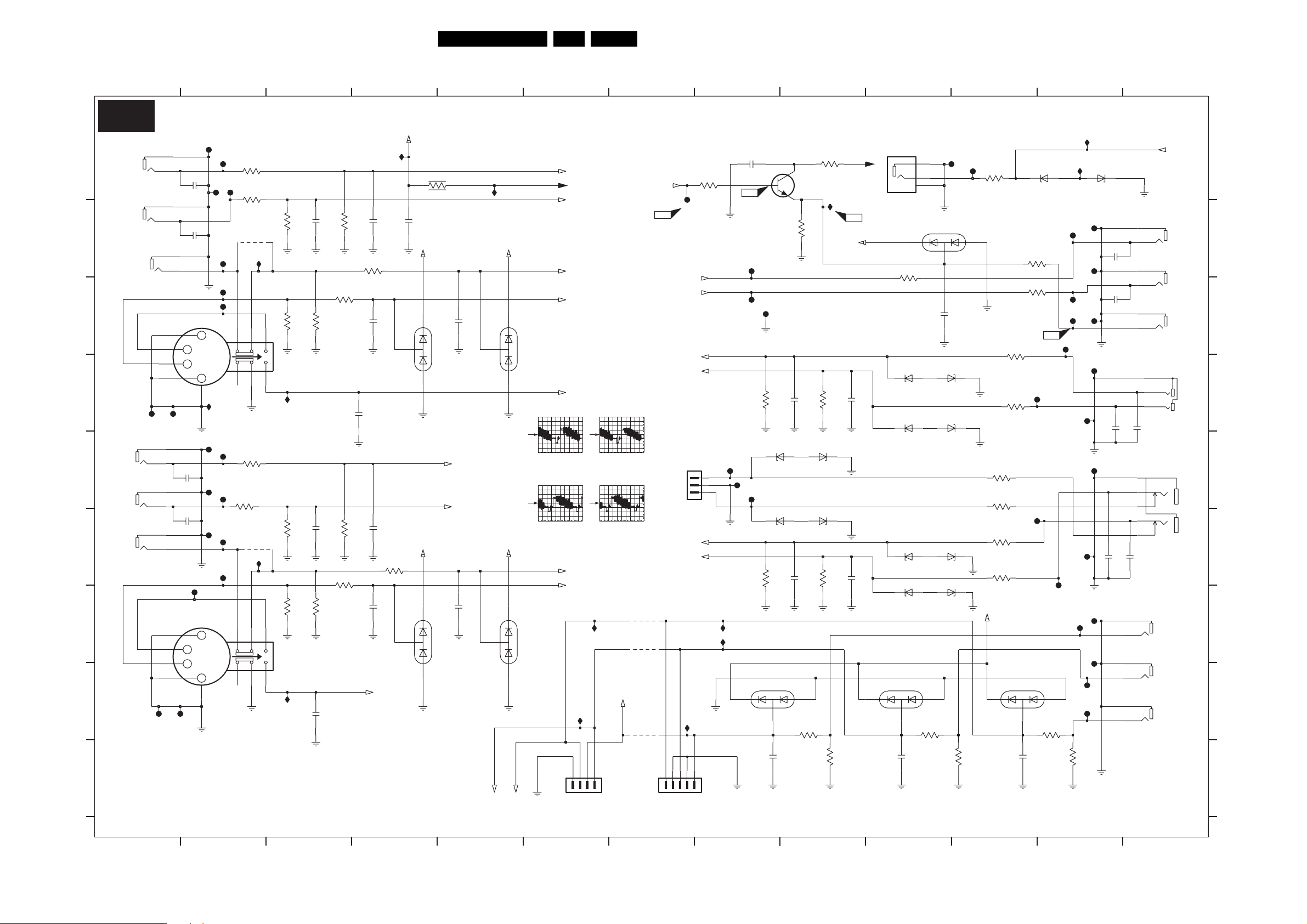
Small Signal Module: AP
C2
C2
Circuit Diagrams and PWB Layouts
31DPTV465 7.
A
A
B
B
C
C
D
D
E
E
F
F
H
H
1 1010
C2
SMALL SIGNAL MODULE (AP)
2
2
3
4
5
543 12
6
7
7
88
91
9
C2
S-2
I217
330p
22p
330p
22p
3051
100R
+Vp
2102
8.5V
100n
+Vp
+Vp
3142
1R0
8.5V
1-D2
1-E2
8.5V
6018
6021
BAV99
BAV99
2069
AV2 -L
AV2-R
2072
22p
22p
I218
+Vp
+Vp
8.5V
6020
8.5V
6023
AV1-L
1-D2
+9V
AV1-R
1-E2
AV1-Y_CVBS
1-B2
AV1-C
1-C2
BAV99
S-1
1-F5
V1
1
500mV / div AC
10µs / div
V3
1 1
500mV / div AC
10µs / div
AV2-Y_CVBS
1-B2
AV2 -C
1-C2
BAV99
I224
I225
CVBS-SC2_MON-OUT
V2
1
500mV / div AC
10µs / div
V4
500mV / div AC
10µs / div
Y
3-B9,1-A2
9011
9012
9013
6-D4
F251
V1
L-CL_VL-OUT
R-CL_VL-OUT
AV4 -R
AV4-L
1
2
3
1011
B3B-EH-A
AV5 -R
AV5-L
I226
3145
1K0
6-F3
6-F7
I228
I227
1-E2
1-D2
1-E2
1-D2
F222
2104
100n
V2
F249
F223
2.5V
F247
F248
47K
3006
6032
BZX284-C6V8
F224
6037
BZX284-C6V8
47K
3007
BAV99
6024
2075
2079
2080
22p
8.8V
7016
BC847B
1.8V
1K0
3146
330p
BZX284-C6V8
BZX284-C6V8
330p
3057
100R
3008
6016
6038
3009
3144
10R
3106
I221
47K
47K
2081
2082
75R
AV1 IN
L
A2
R
V
A3
AV2 IN
1024-11
YKC21-2921
L
D2
1024-10
YKC21-2921
R
D1
1024-12
YKC21-2921
V
D3
F234
1024-2
YKC21-2921
1024-1
YKC21-2921
A1
1024-3
YKC21-2921
F225
20
23
19
22
21
24
2
3
8
7
F233
2
5
2824
1n0
1
4
2825
1n0
3
6
F242
2
3
8
7
F244F243
2822
1n0
2823
1n0
F231
1025
YKF51-5347
1
F235
F237
F239
1026
YKF51-5347
1
F228
I208
F226
F229
F230
F236
F238
F241
F240
F227
94
100R
94
3050
3045
100R
3046
100R
4017
105
3049
100R
10
5
I216
4016
I204
47K
2062
3002
75R
3102
3004
3104
I200
I209
47K
75R
3103
2066
3105
2077
116
116
330p
75R
330p
75R
330p
3003
3048
100R
3005
3052
100R
2076
1-F5
47K
47K
2063
3047
100R
2068
330p
2067
2071
V3
+Vp
330p
330p
+9V
8.5V
6028 BAV99
1029
YKC21-3416
3101
150R
6026
BZX284-C6V8
6022
BZX284-C6V8
6017
BZX284-C6V8
6012
BZX284-C6V8
2074
1
22p
3
2
2070
BZX284-C6V8
BZX284-C6V8
BZX284-C6V8
BZX284-C6V8
3058
100R
F200
6014
BAV99
6027
6025
6019
6013
22p
3107
F201
75R
11
3073
150R
3012
100R
3013
100R
3055
100R
3056
100R
+Vp
8.5V
BZX284-C6V8
3053
100R
3054
100R
F212
6029 BAV99
2073
3100
68R
3072
150R
F211
22p
6031
V4
3059
100R
F215
F209
12
I240
F203
F205
F206
F210
F214
F217
3108
I241
6030
BZX284-C6V8
F202
F204
F207
F208
F213
2829
F216
F218
F219
F221
75R
2831
1n0
2830
1n0
2826
1n0
2827
1n0
2828
15
YKC21-2921
18
14
YKC21-2921
17
13
YKC21-2921
16
13
13611
SUB_WOOF
8-C12
8
YKC21-2921
11
7
YKC21-2921
10
9
YKC21-2921
12
AV OUT
1
2
3
1n0
1
4
5
2
3
1n0
1024-9
1024-8
1024-7
1024-5
L
B2
1024-4
R
B1
1024-6
V
B3
1021
JPJ9811-01-320
1027
JPJ9822-01-320
Y
C3
Pb
C2
Pr
C1
A
A
B
B
C
C
D
D
E
E
F
F
G
G
H
H
I
I
3135 033 3345.7
1
3-E9
3-H9
Pb
Pr
21
384
4
58
5
6
4
GND
N/U
1207
B4B-EH-A
123
Y
Pr
Pb
4
5
GND
N/U
7
7
GND
123
B5B-EH-A
1031
91110
96
11
12
12
E_15000_012.eps
1332 10
13
141004
I
I
Page 32
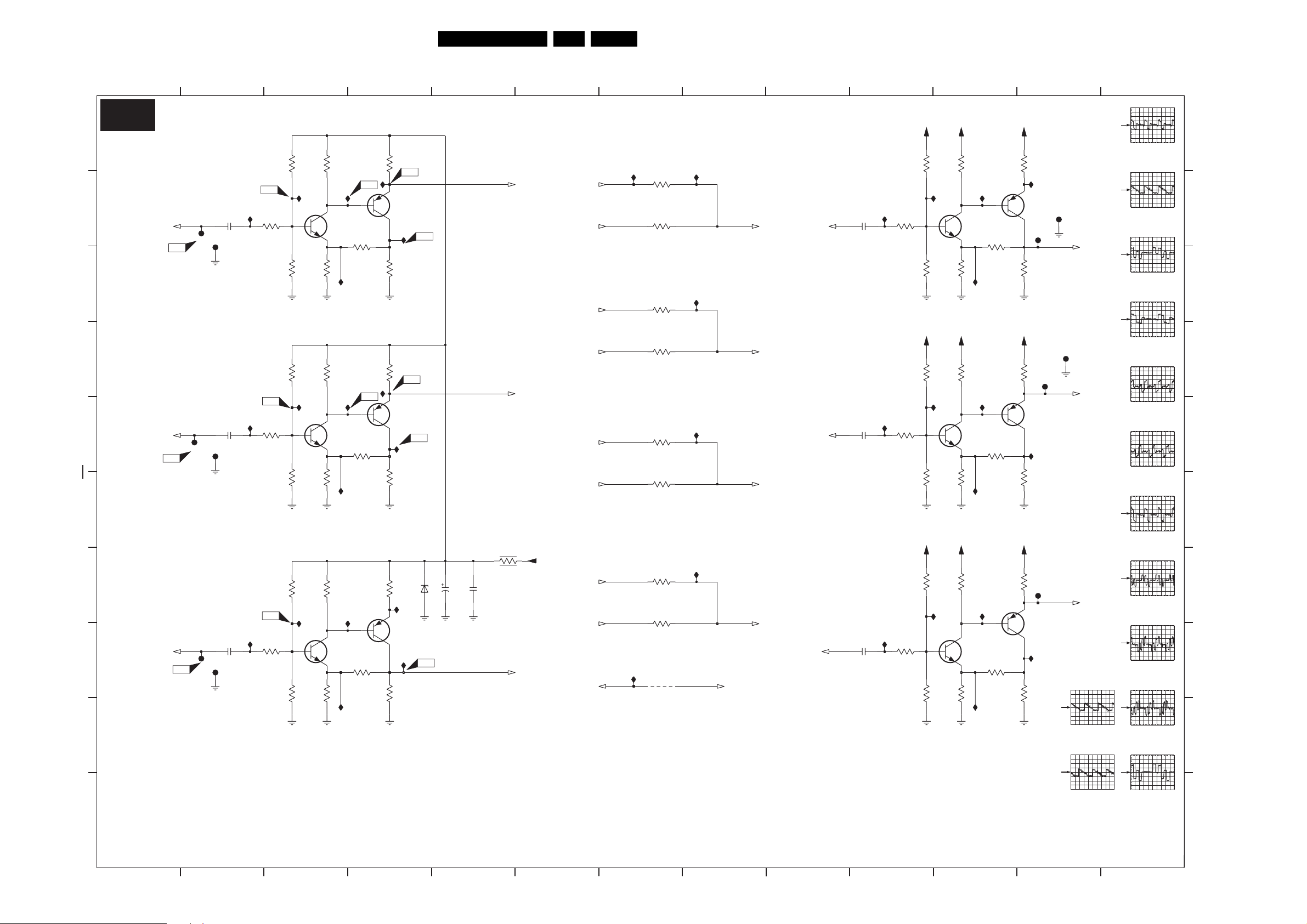
Small Signal Module: AP
C3
Circuit Diagrams and PWB Layouts
32DPTV465 7.
A
A
B
B
C
C
D
D
E
E
F
F
1
1
C3
2 10
23 1111
3
4
4
SMALL SIGNAL MODULE (AP)
68K
V-S SB
U-SSB
3852
V9
I315
6-D4
F304
V6
6-D7
F302
V8
2811
2u2
F305
2809
2u2
F303
3851
100R
3853
3842
V13
I308
3841
100R
3843
I316
4.1V
4V
68K
68K
68K
I309
3.4V
3.3V
3854
7808
BC847B
3855
3844
7810
BC847B
3845
680R
I318
6.8V
680R
I317
680R
I311
6.8V
680R
I310
3856
680R
3846
680R
V10
V14
I319
4.7V
I312
4.6V
3857
BC857B
7809
3858
3847
BC857B
7811
3848
680R
7.4V
I320
22K
680R
7.5V
I313
22K
V11
V15
V16
V12
5
5
8-G8
V-SSB-N
U-SSB-N
8-G8
6
6
RTXT
R_OSD
GTXT
6-B2
G_OSD
BTXT
B_OSD
6-C7
6-B2
6-C7
6-C7
6-B2
I321
7
7
3304
10R
3305
10R
3313
10R
3314
10R
3321
10R
3322
10R
8
813
I322
REDTXT
8-H12
I323
GRNTXT
8-H12
I324
BLUTXT
8-H12
9
Y
2-H7,1-A2
Pb
2-I5
2801
2u2
2803
2u2
I339
I333
109
3801
10R
3811
10R
+9V
3802
1.6V
3803
+9V
3812
3813
I340
2V
I334
100K
27K
100K
39K
.9V
1.3V
+9V
3804
4.8V
7800
BC847B
3805
+9V
3814
7802
BC847B
3815
1K0
5.4V
I341
1.3V
3806
180R
150R
I342
1K0
5.6V
I336
5V
1.9V
3816
470R
270R
I335
3807
3808
3817
3818
+9V
1K0
BC857B
7801
F306
1K0
+9V
1K0
BC857B
7803
1K0
I344
I338
F308
12
12
F307
6-C6
F309
6-C4
G-SC1-IN_Y-IN
B-SC1-IN_U-IN
13
V6
500mV / div AC
10µs / div
V7
500mV / div AC
10µs / div
V8
500mV / div AC
5µs / div
V9
500mV / div AC
5µs / div
V10
200mV / div AC
10µs / div
V11
200mV / div AC
10µs / div
V12
A
A
B
B
C
C
D
D
E
E
F
F
H
H
500mV / div AC
10µs / div
V13
500mV / div AC
10µs / div
V14
200mV / div AC
10µs / div
V15
200mV / div AC
10µs / div
V16
500mV / div AC
5µs / div
G
G
HH
I
I
J
J
6V
1.6V
3827
3828
+9V
1K0
BC857B
7805
I331
1K0
F310
R-SC1-IN_V-IN
6-C4
V17
500mV / div AC
10µs / div
V18
500mV / div AC
10µs / div
I328
100K
39K
1.5V
+9V
3824
5.4V
7804
BC847B
3825
1K0
I330
3826
100R
330R
I329
3821
10R
+9V
3822
2.1V
3823
3809
10R
68K
3832
V17
I301
6-D4
Y-SSB
F300
V7
I
I
J
J
2807
2u2
F301
3831
100R
3833
2.8V
39K
I302
2.2V
3834
7806
BC847B
3835
10R
680R
I304
I303
3836
100R
3837
BC857B
7807
3838
680R
I306
*
I305
330R
N/U
6801
V18
2813
470u 25V
BZX384-C9V1
2814
100n
8-F8
Y-SSB-N
+15V
FBLTXT
FBL
FRAMEDRIVE-
6-B2
6-C7
6-E4
I326
3329
10R
3330
10R
4005
I325
6-H7,6-E11
VFB
8-H12
TXTFBL
I327
2-I5
2805
2u2
Pr
3135 033 3345.7
1
7
2 12 1326498
3
4
53
65
7
10
E_15000_013.eps
191004
111
111098
1312
Page 33
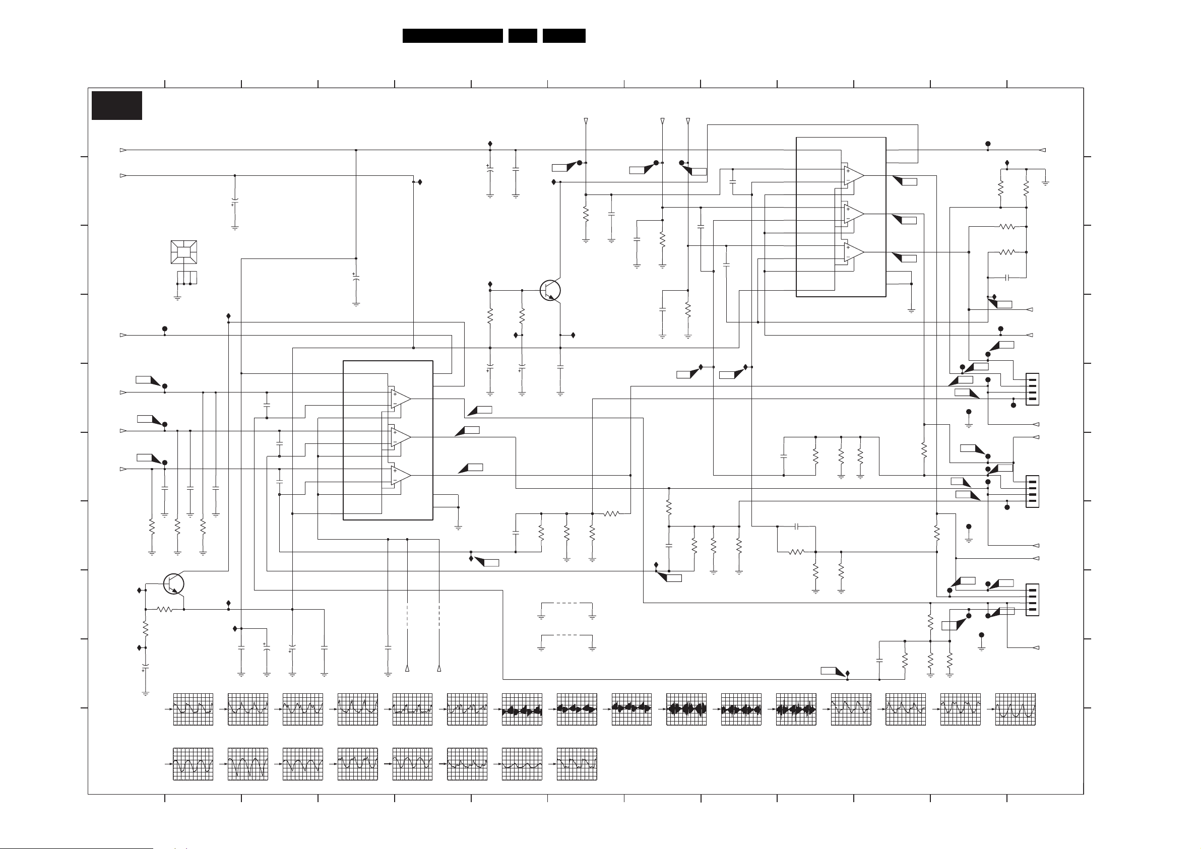
Small Signal Module: AP
C4
Circuit Diagrams and PWB Layouts
33DPTV465 7.
A
A
B
B
C
C
D
D
E
E
F
F
G
G
H7H
I
I
C4
+35V
-35V
VccPSW-H
BH
GH
RH
1
1
2
2 11D11
3103
SMALL SIGNAL MODULE (AP)
6-H11,5-A1
6-G11,5-I12,4-I5
2028
100u
GND-C
0045
HEATSINK
5-B1
6-C11
6-C11
6-C11
I401
I400
26.2V
G1
G2
G3
GND-C
-36.9V
3034
2043
GND-C
3092
22K
10u
F403
F402
F401
F400
2060
3K3
3167
4K7
GND-C
150p
GND-C
3091
GND-C
G1
2057
3K3
-35.8V
7007
BC817-25
-36.9V
150p
GND-C
3090
GND-C
2056
3K3
I408
150p
GND-C
I402
I403
2133
GND-C
100n
35.7V
-.5V
2100
150p
-.5V
-36.9V
-.05V
2101
150p
-.05V
-36.9V
.2V
2112
150p
.2V
-22V
-36.9V
100n
2032
100u
2037
GND-C
GND-C
G3G2 G7
100u
2132
GND-C
45 9
4 106
5
I438
8
6
7
BV
6-C11
8
RV
GV
6-B11
6-C11
9
35.6V
F405
150p
3099
F406
3K3
G9
2064
150p
2051
150p
-.1V
-.1V
-24.5V
.01V
-24.5V
.05V
I410
2008
GND-C
100u
2131
GND-C
100n
I412
G7
F404
3147
GND-C
3K3
2026
GND-C
G8
150p
2096
.04V
-24.5V
-36.9V
6R8
G12 G13
1
2113
2030
GND-C
PRE_POS
5
CH1_IN_POS
6
CH1_IN_NEG
7
CH1_NEG
8
CH2_IN_POS
14
CH2_IN_POS
13
CH2_NEG
12
CH3_IN_POS
15
CH3_IN_NEG
16
CH3_NEG
17
PRE_NEG
4
100u
I416
-35.8V
-36.9V
-36.9V
VCC
MUTING
CH1_OUT
26.2V
10
3
-35.8V
9
.8V
3169
2038
GND-C
4K7
100u
I411
3033
2042
GND-C
22K
10u
2130
GND-C
G4
G5
GND
.6V
11
7044
STK392-120
18
.8V
1
2
GND-C
9045
6-G11,5-I12,4-B1
-35V
G6
I404
G6
G15
150p
3095
GND-C
GND-C
3K3
G8
1
2109
CH2_OUT
CH3_OUT
SUB_GND
9044
100n
2134
6-H11,5-I1
GND-C
-22V
G5G4 G10 G11G9
7005
BC817-25
I417
100n
3154
GND-C
9009
9010
6R8
3153
GND-C
6R8
3162
100R
150p
3094
3K3
3K3
GND-C
3152
2065
G16
6R8
1
I420
3151
GND-C
GND-C
GND-C
150p
2061
3148
GND-C
GND-C
I421
G17
3161
100R
2107
150p
I427
G14
PRE_POS
5
CH1_IN_POS
6
CH1_IN_NEG
7
CH1_NEG
8
CH2_IN_POS
14
CH2_IN_POS
13
CH2_NEG
12
CH3_IN_POS
15
CH3_IN_NEG
16
CH3_NEG
17
PRE_NEG
4
150p
2111
150p
3096
3K3
10
3097
3157
GND-C
7045
STK392-120
3K3
6R8
3155
GND-C
6R8
6R8
3158
GND-C
G13
CH1_OUT
CH2_OUT
CH3_OUT
SUB_GND
3156
GND-C
I429
VCC
MUTING
GND
6R8
2105
10
11
18
G14
3
9
1
2
150p
24V
-35.8V
.5V
G10
.1V
G11
.5V
G12
GND-C
3093
3K3
3164
3166
3150
GND-C
12 13
12
F407
F410
G19
F411
G6
G20
F423
GND-C
G11
100R
G5
F413
F414
F415
G22
F422
3163
100R
GND-C
G23
G24
F420
3149
F417
F421
GND-C
6R8
F418
100R
6R8
GND-C
G15
F409
F419
3160
I435
G18
F408
G16
I436
3165
100R
3098
3K3
2115
150p
G12
G21
F416
G10
G4
6R8
5-G12
B4P-VH
F412
3159
5-A6
1005
5-F4
5-A6
B4P-VH
5-F4
5-A6
B4P-VH
5-F4
5-D12
6R8
RV_OUT
VccNSW-V
1006
1007
13
VccPSW-V
GND-C
1
RV-OUT
RV-RET
2
RH-OUT
3
4
RH-RET
RH_OUT
GV_OUT
1
GV-OUT
2
GV-RET
3
GH-OUT
4
GH-RET
GH_OUT
BV_OUT
1
BV-OUT
BV-RET
2
3
BH-OUT
BH-RET
4
BH_OUT
TO RED YOKE
TO GREEN YOKE
TO BLUE YOKE
A
A
B
B
C
C
D
E
E
F
F
G
G
H
H
I
I
J
J
3135 033 3345.7
1
1V / div AC
10µs / div
G17
1V / div AC
10µs / div
2 11
1V / div AC
10µs / div
G18 G20G19
1V / div AC
10µs / div
32 13
3
1V / div AC
10µs / div
1V / div AC
10µs / div
10V / div AC
10µs / div
1V / div AC
10µs / div
4
10V / div AC
10µs / div
1V / div AC
10µs / div
54
5
10V / div AC
10µs / div
G22G21
1V / div AC
10µs / div
2V / div AC
5ms / div
1V / div AC
10µs / div
6
6
2V / div AC
5ms / div
G24G23
1V / div AC
10µs / div
20V / div AC
5ms / div
7
7
10V / div AC
8
8
5ms / div
10V / div AC
5ms / div
9
9
1V / div AC
5ms / div
10
1V / div AC
10µs / div
1V / div AC
10µs / div
11
1V / div AC
10µs / div
12
12
1V / div AC
10µs / div
E_15000_014.eps
191004
131
J
J
Page 34
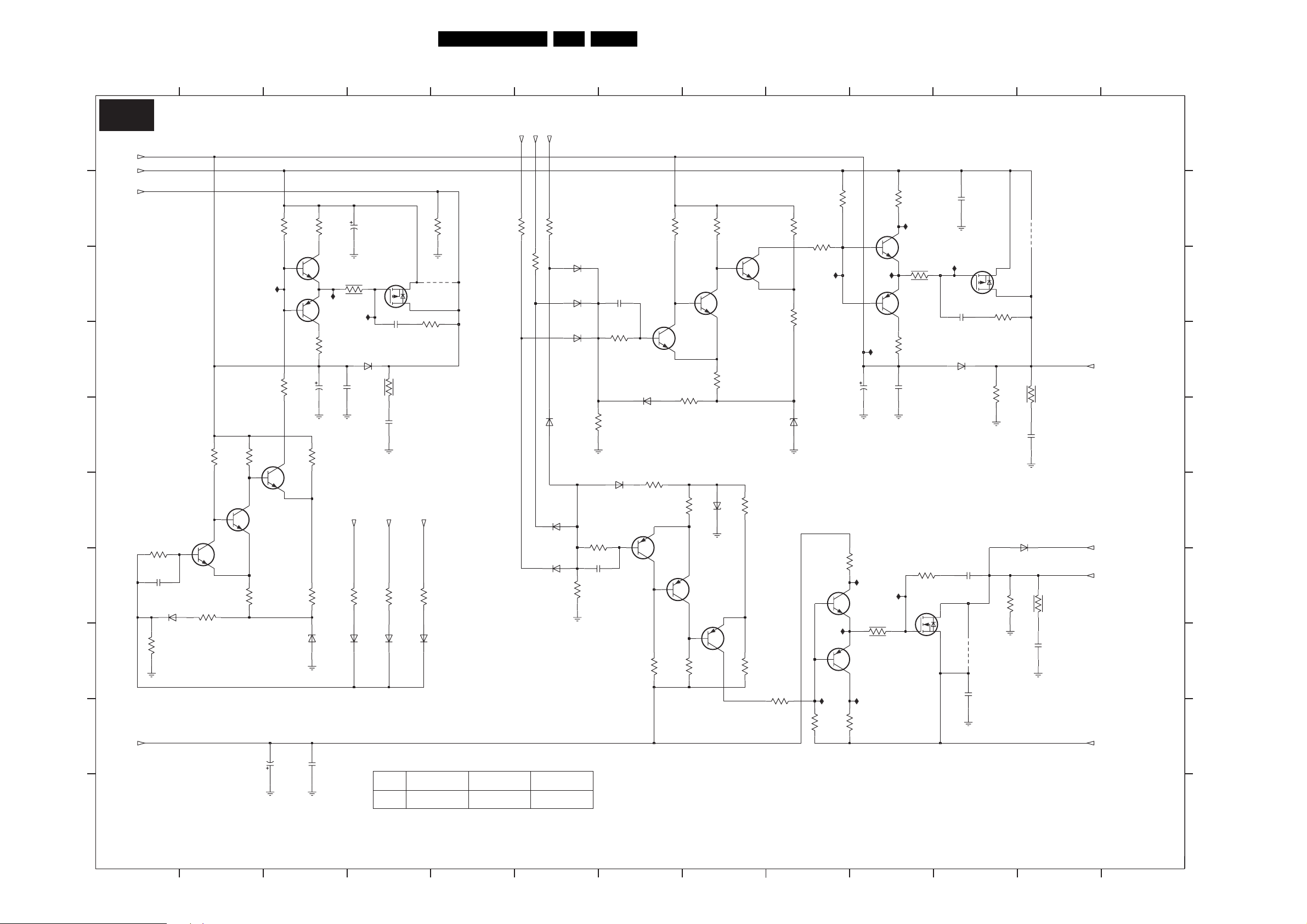
Small Signal Module: AP
C5
Circuit Diagrams and PWB Layouts
34DPTV465 7.
3074
3K3
3079
3170
6044
GND-C
99
10K
3199
3K3
I509
680R
BZX284-C6V8
I515
I514
2K7
3041
3196
2K7
3077
7012
BC817-25
7013
BC807-25
3065
12
3082
GND-C
33K
9040
2050
3083
2052
GND-C
12
4-A13
10R
1n0
6-G11,6-C9
4-D13
10R
1n0
6-G11,4-B1,4-I5
10 11 13
10
1n0
2156
GND-C
I519
2157
1n0
6006
BYD33D
IRF9Z24N
1
2160
1n0
2161
GND-C
9041
7020
100n
3084
GND-C
3
2
3201
10R
33K
6008
BYD33D
3086
GND-C
2058
GND-C
470R
I517
I516
470R
I510
470u
3061
6R8
I520
GND-C
I518
470R
3197
7010
BC817-25
7011
BC807-25
470R
3200
1n0
2159
STP16NE06
I521
3198
6R8
3202
10R
7022
134
VccPSW-V
-22VR
VccNSW-V
-35V
8
8
A
A
1
1
C5
+22V
+35V
VccPSW-H
26
2
45
SMALL SIGNAL MODULE (AP)
6-H11
6-H11,4-A1
4-D1
53
611
BV_OUT
RV_OUT
GV_OUT
4-E13
4-D13
4-G13
7
7
B
8K2
3044
3035
8K2
6045
6046
BAS216
6047
BAS216
8K2
BAS216
BAS216
BAS216
BAS216
6042
6041
6040
3020
GND-C
3031
GND-C
100R
2040
330p
100K
3037
2035
330p
3038
100R
100K
6048
BAS216
6043
BAS216
3062
3K3
3019
7001
BF550
220K
3043
7015
PMBT2369
3032
220K
3K3
3060
3036
100R
7006
BF550
BC857B
4K7
3080
3063
6049
GND-C
7014
4K7
7018
PMBT2369
100R
BZX284-C6V8
3064
3066
7019
BC847B
680R
10K
3137
6051
3085
GND-C
9042
3193
10R
RH_OUT
4-E13
8K2
BAS216
33K
3042
2K7
3K3
7004
BC847B
2153
GND-C
3112
3132
6033
GND-C
3191
470R
7009
BC817-25
I505
7008
BC807-25
3195
470R
100u
10K
680R
BZX284-C6V8
3190
4K7
3168
7023
PMBT2369
3133
I504
3194
100R
C
C
D
D D
E
E
3110
220K
FF
7024
PMBT2369
3134
100R
2044
G
G
H
H
I
I
-22V
330p
3078
GND-C
6-H11,4-I5
6035
BAS216
100K
3067
3K3
2150
GND-C
2154
GND-C
3192
6R8
3135
6039
100u
I503
BYD33D
6007
1n0
BH_OUT
4-H13
8K2
BAS216
7021
IRF9Z24N
1
2152
1n0
3081
2047
GND-C
GH_OUT
3136
6050
3
2
10R
1n0
4-G13
8K2
BAS216
A
A
BB
B
C
C
D
E
E
F3F
GG
H
H
I
I
J
J
3135 033 3345.7
1
2059
GND-C
2
24
GND-C
3 10 13
3
Ref Des 3135_037_11351_01
CHINA CORE
3190 NOT USED NOT USED 319802152720
3135_037_11361_01AP3135_037_11371_01
41
1n0
2055
470u
NAFTA CORE
(KOREA)
2K7
65
65
J
J
E_15000_015.eps
061004
7
7
8
8
9
10
11
119
12
12
13
Page 35
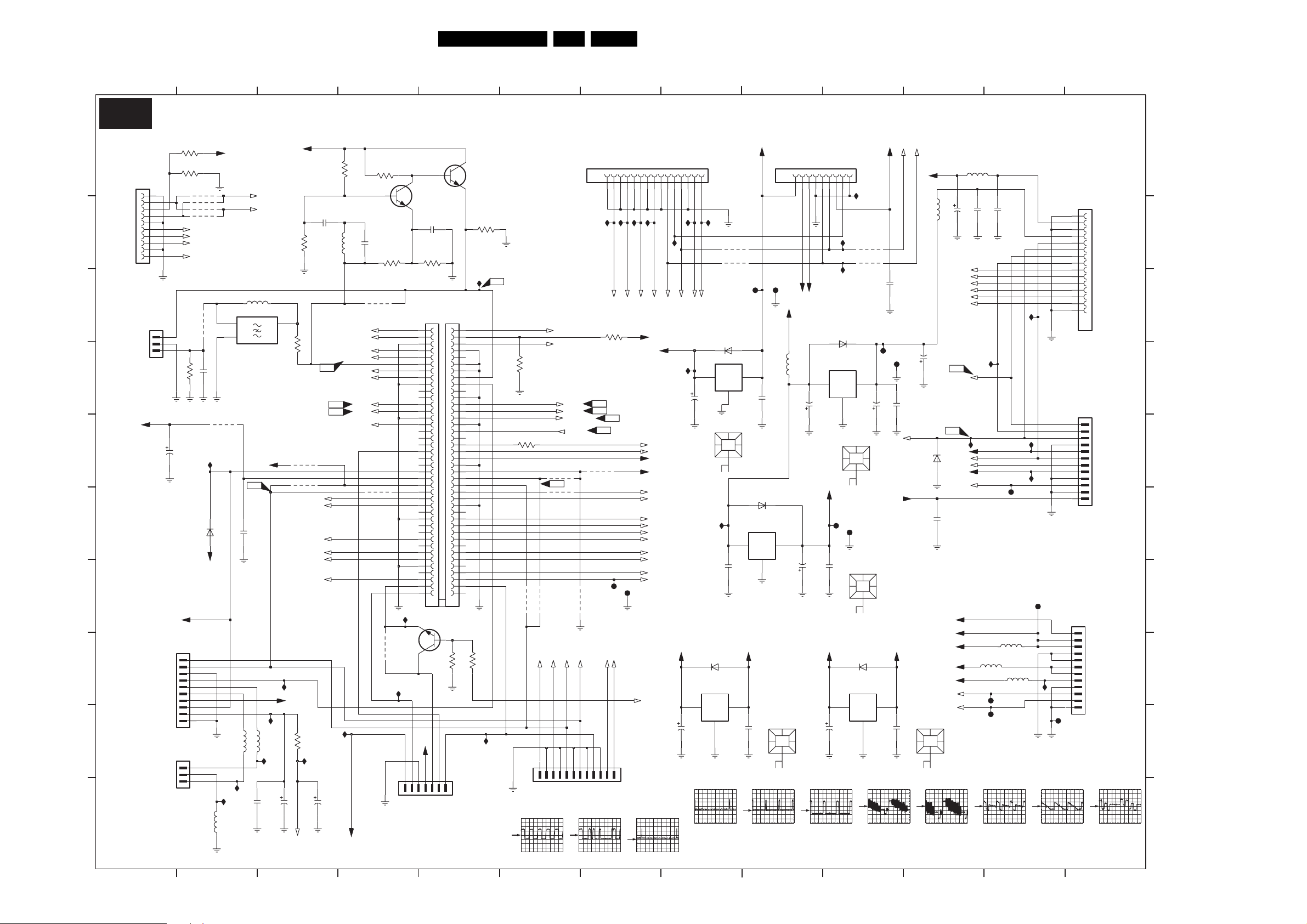
Circuit Diagrams and PWB Layouts
C6
35DPTV465 7.
Small Signal Module: AP
3
1 8
21
2
3
46
5
64
7
7
8
9
9
10
1110
11
12
12
135
13
C6
A
A
10
GND
9
TXD
8
GND
7
RXD
6
GND
5
RTXT
TO SSB
B
B
C
C
D
D
E
E
F
F
G
G
H
H
STATUS_1_PIP-AFT_50-60HZ
I
I
J
J
3135 033 3345.7
4
GTXT
3
BTXT
2
GND
1
FBLTXT
10FMN-BTRK-A
CVBS-PIP_
TUN1-2-CVBS-IN
GND
CVBS_TER_OUT
TO PIP
+5V
TO PIP
1
1
1043
SMALL SIGNAL MODULE (AP)
1
2
3
B3B-EH-A
1272
SDA_IN
SCL_IN
GND
VFB_PIP
HFB_PIP
+33VT2
GND
VFB_PEMG
HFB_PEMG
3-B7
3-C7
3-E7
3-G7
2024
+8V
B10B-EH-A
1
2
3
4
5
6
7
+5V
+8V
8
9
10
B3B-PH-K
3
2
1
3075
3076
10V2m2
1201
1681
1K0
1K0
4020
4021
4022
4023
RTXT
GTXT
BTXT
FBLTXT
1K03018
I613
6-H10,6-A3
4010
I
6004
2045 1n0
+9V
5008
2
2
+5V_STBY
1
2
9017
BYD33D
I600
I601
6-C8
6-C8
I
GND
2034
5006
5009
15u
1200
TPSRD
4M5
C1
100n
2029
TXD
RXD
O
O
+3.3V
6-E7,6-H9
SOUND_ENABLE
Y-CVBS_FRONT-IN
6-H10
I605
5005
I602
47n
2012
+8V
6-H10,6-G2
3070
560R
3
3017
330R
9019
9007
L-SC2_AV2-IN
HEADPHONE_L
L-CL_VL-OUT
AUDIO-L
I606
+5V-PIP
3025
100R
I603
1u0
2002
1-I1
TUNER_B+
3
3
3069
820R
2031
120p
1u0
2048
5010
B-SC1-IN_U-IN
R-SC1-IN_V-IN
C-SC2_SVHS-IN
CVBS-SC2_MON-OUT
V1
IF-TER
AGC
V-S SB
V6
Y-SSB
V7
FRAMEDRIVE-
7-C1
1-I6
1-D13
8-B1
2-B8
7-F1
I604
10u
8-F10,7-A10,7-A11,6-E11,6-E7,6-A2
+5V_STBY
3068
330R
7025
BC847B
2046
5.6V
6V
1.4V
2.5V
2.4V
1.7V
1.5V
1.2V
.09V
.09V
7.9V
4.9V
3.2V
5V
.01V
4.4V
1V
.2V
0V
3.4V
.8V
3.3V
I608
7027
23456
1
+5V_STBY
KEYBOARD
68p
3010
180R
ROW_A
1020-A
8182
87613-8011
+9V
GND
10p
4015
9016
330R
3-D12
3-G12
1-A10
2-A7
1-I1
1-F1
3-B1
3-H1
3-H7
4003
3039
BC817-25
I607
TO FRONT CONTROLS
4
4
ROW_B
1020-B
1
2
4
3
5
6
8
7
9
10
12
11
13
14
16
15
17
18
20
19
21
22
24
23
25
26
28
27
29
30
32
31
33
34
36
35
37
38
40
39
41
42
44
43
45
46
48
47
49
50
52
51
53
54
56
55
57
58
60
59
61
62
64
63
65
66
68
67
69
70
72
71
73
74
76
75
77
78
79
80
8182
3001
7
RC5
ON-OFF-LED
1.3V
1.9V
3.2V
4.4V
4.4V
4.4V
1.3V
1.4V
4K7
1014
5
5
7026
BC847B
I616
1V
2.4V
0V
1.4V
1.4V
.05V
.19V
.5V
0V
5V
0V
5V
.3V
.2V
0V
0V
3.4V
3.1V
3014
B7B-EH-A
3071
1K0
47K
I609
V5
3-B12
1-A11
10K
3182
3111 470R
C1
2V / div AC
5µs / div
G-SC1-IN_Y-IN
Y-CVBS-SC2_AV2-IN
3-E1
8-F8
8-F8
6-D11
4008
C2
4004
4007
SDA-C
1-G10,6-C8
GND
SDA-C
6
6
U-SSB
H-SSB
VSYNC-SSB
HBLANK
4009
SCL-C
1-G10,6-C8
9
101112
GND
SCL-C
19
15JL-BT-E
1000
18
V8
L1
8-F10,7-C12,6-E11
9018
F613
4006
SCL_IN
SDA_IN
1-F12,1-F1,6-A10
1-F12,1-G1,6-A11
5
678
RC5
GND
GND
SCL_IN
SDA_IN
C2
2V / div AC
20µs / div
TO ACS CONTROL
GND
GND
B_OSD
GND
FBL
17
15
16
.2V
.01V
.01V
I617
I618
I619
3-D7
3-G7
3-F7
FBL
B_OSD
G_OSD
3183
15K
F1
L40
6-E3,6-H9
1-G8
1-I6
1-G8
1-B2
1-D13
8-E1
2-C8
8-B9
7-E1
F614
IRQ
VFB
3-H8,6-E11
LED_DRV
8-G10
B12B-EH-A
1033
1
234
TO MMI
VFB
GND
F1
2V / div AC
7
7
G_OSD
GND
GND
R_OSD
1011121314
4.9V
.01V
I620
I622
3-B7
1-G10,6-H6
R_OSD
+5V
+15V
STANDBY
IRQ
+5V_STBY
+3.3V
PWR_FAIL
L-SC1_AV1-IN
R-SC2_AV2-IN
R-SC1_AV1-IN
FRONT-DETECT
C_FRONT-IN
HEADPHONE_R
R-CL_VL-OUT
AUDIO_SW
AUDIO-R
2ms / div
SDA-C
H-HOP
.3V
4.9V
1-G10,6-H6
SDA-C
I623
2054
SCL-C
3456789
I621
SCL-C
2027
+5V
GND
3.3V
6-B2
IN
1u0
F11
TXD
RXD
1
2
3.1V
I635
GND-C
9030
9031
6003
S1D
COM
GND
0103
HEATSINK
I624
2001
OUTIN
F609
OUTIN
7103
L7812CV
-22.1V
IN OUT
100n
OUT
2053
6-A2
TXD
RXD
IN OUT
1u0
6015
S1D
7104
LF33CV
COM
GND
2V / div AC
2ms / div
8
8
+12V
8-B11
6001
S1D
7101
L7912CV
OUTIN
COM
GND
+3.3V
6-E3,6-E7
100n
L1
2V / div AC
10µs / div
13
11
F610
5-F12,6-G11
5011
100n
2005
-11.9V
0104
HEATSINK
9
9
TO WB/HOP
-12V
HOP
+12V
GND
SDA-2
9
12
10
9.1V
6-F10
8-C10
HOP
-12V
-22VR
10u
-22.1V
IN OUT
2007
100u
1u0
2003
2010
2097
L40
2V / div AC
10µs / div
+5V
SCL-2
45678
.3V
I636
S1D
6002
7102
L7908CV
COM
-12V
6-C9
F605
100n
+8V
6-G2,6-A3
IN
7.9V
1u0
GND
H-HOP
123
09JL-BT-E
1950
I638
I637
9033
9032
-7.9V
OUTIN
GND
0102
HEATSINK
F606
0101
HEATSINK
6005
S1D
7105
L7805CV
OUTIN
COM
GND
V1
1 1
500mV / div AC
10
10
F607
F608
2011
5V
10µs / div
+5V
SCL_IN
1-F12,1-F1,6-H6
100n
2006
1u0
100n
2004
3-H8,6-H7
VFB
8-F10,8-G5,8-D7,3-G6,6-D8
+15V
+5V-PIP
6-H3
OUT
0105
HEATSINK
100n
2098
SDA_IN
+9V
1-F12,1-G1,6-H6
5000
2039
10u
6036
+5V_STBY
BZX384-C4V7
2033
-22VR
+V_AUDIO
-V_AUDIO
500mV / div AC
10µs / div
11
10u
2041
GND-C
L40
HBLANK
F11
I632
+33V
STANDBY
+130V
PWR_FAIL
100n
-35V
-22V
+22V
+35V
5001
10u
10u
2049
100n
2036
100n
GND-C
4-A8
RV
4-F1
RH
4-A8
GV
4-E1
GH
4-A7
BV
4-E1
BH
I640
6-E7
10u
F602
10µs / div
5004
10u
F600
5003
10u
I631
I630
12
12
1-J1
8-F10,7-C12,6-E7
8-F10,7-A10,7-A11,6-J4,6-E7,6-A2
1-J1
7-A9,6-E7
5-I12,4-B1,4-I5
5-F12,6-C9
5-I1,4-I5
5002
5-A1
5-A1,4-A1
7-H12
7-G12
F603
500mV / div AC
8.9V
-7.9V
.8V
.09V
-.05V
-.1V
-.5V
I639
GND-C
.09V
.3V
14.6V
F615
I628
F604
GND-C
V7V6V5 V8
500mV / div AC
10µs / div
1001
15JL-BT-E
16
18 19
1518
B12B-EH-A
1516
B12B-EH-A
1
2
3
4
5
6
7
8
9
10
11
12
GND
1
+9V
2
GND
3
-8V
4
STANDBY
5
VFB
6
HBLANK
7
DEF_GND
8
9
RV
10
RH
GV
11
GH
12
BV
13
BH
14
GND
15
17
HBLANK
1
DEF_GND
2
VFB
3
GND
4
+33V
5
STANDBY
6
+5V_STBY
7
+130V
8
GND
9
PWR_FAIL
10
GND
11
+15V
12
-35V
-22V
-22V
GND-C
GND-C
+22V
+22V
+35V
GND
+V_AUDIO
-V_AUDIO
GND
E_15000_016.eps
13
1311
TO LARGE SIGNAL
500mV / div AC
5µs / div
141004
A
A
B
B
TO ACS CONTROL
C
C
D
D
E
E
TO LARGE SIGNAL
F
F
G
G
H
H
I
I
J
J
Page 36
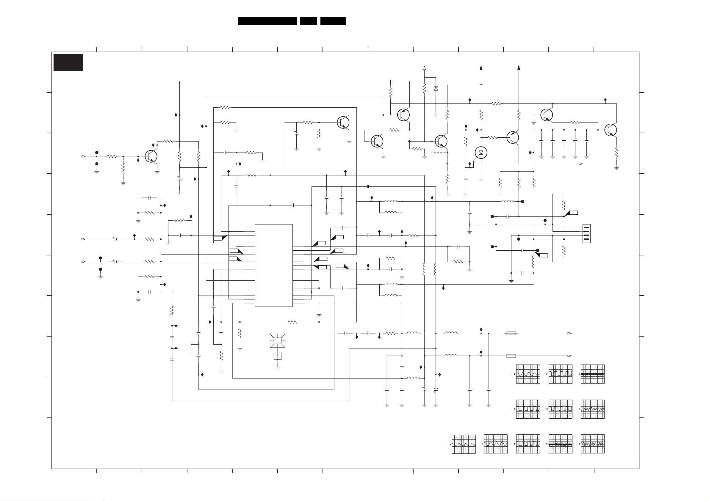
Small Signal Module: AP
C7
Circuit Diagrams and PWB Layouts
36DPTV465 7.
A
A
B
B
C
C
D
D
E
E
F
F
H
H
1
1
C7
SOUND_ENABLE
AUDIO-R
AUDIO-L
32
3
4
SMALL SIGNAL MODULE (AP)
3708
6-F3
6-G7
6-G3
F700
F701
F702
F703
3701
10K
50V
50V
2701
2703
1u0
1u0
100K
3727
I711
I708
.01V
I713
2702
1n0
3790
4K7
3793
10K
3792
10K
3791
4K7
2704
1n0
5.2V
7701
BC847B
I707
I750
3702
6K8
3705
2708
2720
I714
3703
2705
3712
10K
2718
22p
10R
220n
220n
I704
I702
33K
1u0
I738
I710
I709
3704
2706
2707
10K
100n
100n
I751
I705
2722
56K
3706
5K6
2709
470p
I718
A1
470p
2721
3722
470p
68K
12
126
7705
BC847B
2u2
2775
2776
8-F10,6-E11,6-E7
3732
3733
6-H11
6-H11
3730
100R
2u2
2773
2K2
A10
26-62-6051
2K2
-V_AUDIO
+V_AUDIO
2u2
2774
STANDBY
1349
A9
1
2u2
1
2
3
5
PWR_FAIL
47K
5710
9
9104
6-E11,6-E7
3799
BZX284-C6V8
.06V
4018
I724
5709
I735
6702
1V
100R
7711
BC847B
100K
I743
5713
10u
5714
10u
3795
3789
2716
330p
3710
22K
I726
3713
2713
I725
I728
2777
102
+5V_STBY
8-F10,6-A2,6-E7,6-E11,6-J4,7-A11
3715
47K
3K3
3726
I727
3719
680n
I745
I744
F709
1K0
1702
F708
BT169B
3796
100R
100n
1111
+5V_STBY
8-F10,6-A2,6-E7,6-E11,6-J4,7-A10
1K0
3720
5V
10K
5716
2737
10n
T
.8V
F706
1701
MRT
2000mA
1700
MRT
BC857B
7708
3717
2736
2763
680n
T2000mA
A3
I729
100K
F704
10n
5V
3718
5715
F705
F707
2778
100K
A11
5.2V
.04V
2u2
A6
5.1V
I721
I746
88
3716
7707
BC847B
5703
68u
5701
68u
2719
1n0
3725
22K
2728
330p
5704
68u
5702
68u
3724
100R
5.2V
3714
47K
47K
5.2V
I722
I736
2724
I720
BC857B
7706
.06V
3709
100R
5711
220n
5712
3794
100K
I742
5
5
3707
68K
I717
3711
120K
470p
2710
-16.8V
14
CURREF
8
2.6V
OSC
7
0V
FEED1
9
-.1V
.04V
5.1V
-7.6V
5.3V
18V
18.1V
0V
0V
0V
5K6
FEED2
IN110IN1
IN218IN2
FEED317FEED3
FEED419FEED4
6
STBY-MUTE
25
VREG
+5V12+5V
4
+VCCPOW1
22
+VCCPOW2
HEATSINK
0001
-VCCSIGNSUB
-VCCPOW1
-VCCPOW2
A8
A9
3721
BOOT15BOOT1
OUT1
OUT1
OUT223OUT2
BOOT221BOOT2
NC1
GND
T111T1
T215T2
-5V
2735
2712
220n
7700
TDA7490
20
13
24
3723
56K
3
1
16
2
6
-.1V
9.3V
2.6V
2.1V
9.3V
.05V
-18V
-5.3V
-18V
-18.1V
10u
3798
47K
100K
7
7
5.1V
.3V
7710
3797
BC847B
.06V
I719
I703
220n
I747
I723
2715
1n0
I739
2711
1n0
220n
2723
2725
2714
33n
A4
A2
A6
A7
A3
A5
2726
33n
2727
1n0
.04V
RIGHT
GND
GND
LEFT
13
13
I730
5.2V
7704
BC847B
3731
100R
TO CENTER CHANNEL
A
A
B
B
C
C
D
D
E
E
F
F
G
G
H
H
I
I
JJ
3135 033 3345.7
1
1
2V / div AC
2m2
220n
2732
2733
7
2610
2
3
3
4
4
59
5
6
7
8
220n
2731
2730
9
2m2
A1
2V / div AC
500ns / div
2780
100n
10
2781
A2
2V / div AC
2µs / div
100n
2µs / div
A4
20V / div AC
2µs / div
A5
20V / div AC
2µs / div
11
11
20V / div AC
2µs / div
A7
20V / div AC
2µs / div
A8
1
200mV / div AC
50µs / div
12
12
200mV / div AC
50µs / div
A10
500mV / div AC
5µs / div
A11
200mV / div AC
5µs / div
E_15000_017.eps
191004
13
138
I
I
J
J
Page 37
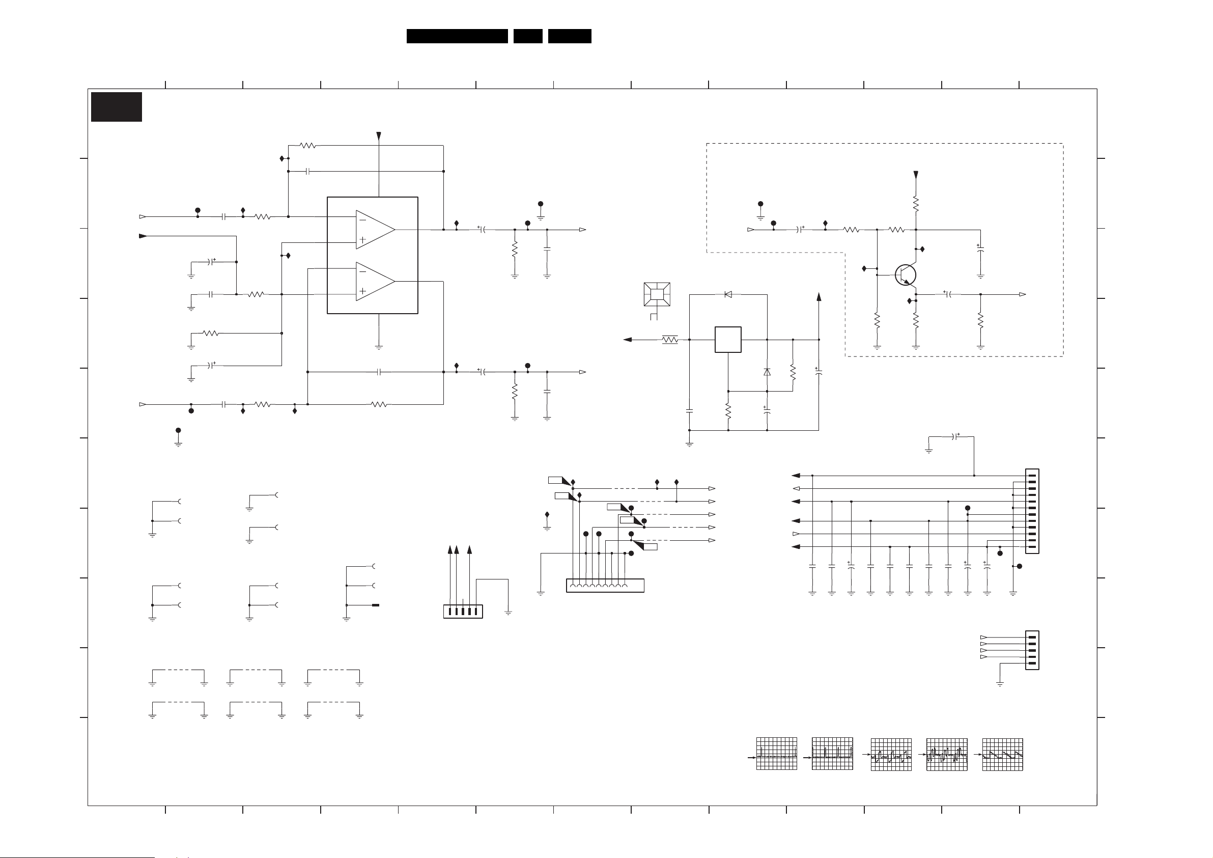
Small Signal Module: AP
C8
Circuit Diagrams and PWB Layouts
37DPTV465 7.
A
A
B
B
C
C
D
D
E
E
F
F
H
H
I
I
1
11
C8
HEADPHONE_L
+5V
HEADPHONE_R
2
2
31
3
4
4
SMALL SIGNAL MODULE (AP)
+5V
3412
33K
2414
100p
INA_NEG
2
2.4V
INA_POS
3
2.4V
I814
I810
1
1
1
1
GND-C
6
2.4V
5
2.4V
INB_NEG
INB_POS
9048
9047
2417
100p
3416
1611
SIN-21T-1.8S(B)
1602
SIN-21T-1.8S(B)
1603
RTB-1.5-1F
84
VDD
VSS
33K
1
1
6-F3
6-F7
GND-C
1606
SIN-21T-1.8S(B)
1607
SIN-21T-1.8S(B)
1608
SIN-21T-1.8S(B)
1609
SIN-21T-1.8S(B)
9037
9038
F800
F801
1
1
1
1
F802
100u
100u
2412
2413
100n
3415
3K3
2421
50V
50V
2411
470n
2423
470n
GND-C
I813
I811
3423
GND-C
3422
10K
3K3
3418
10K
1604
1605
1601
1600
9046
9039
I815
SIN-21T-1.8S(B)
SIN-21T-1.8S(B)
SIN-21T-1.8S(B)
SIN-21T-1.8S(B)
4.9V
1
OUTA
OUTB
5
1
2.4V
7403
TDA1308
7
2.4V
1206
B5B-EH-A
I816
2467
50V
100u
I809
2418
50V
100u
+9V
+5V
+15V
1
2
345
USED ON CERTAIN
MODELS ONLY
65
6
3419
3420
F804
10K
F806
10K
F805
2415
2416
I807
GND-C
3139
2440
50V
430R
6-H7
2110
2818
10
10
6-C9
I819
HOP
10n
47u
2819
10n
3442
1K0
2817
I822
25V100u
11 12
11 12
+12V
3441
3440
100K
7415
BC847B
I821
2820
3447
10n
100K
2821
10n
2009
3443
100n
6-A9
220R
I820
470R
2815
100n
2441
2816
2802
10u50V
16V220u
F611
100n
BLUTXT
GRNTXT
REDTXT
2140
TXTFBL
2442
3444
100u
2141
100K
3-G8
3-F8
3-D8
3-B8
220u
F816
100u
2-A13
SUB_WOOF
1102
B12B-EH-A
F612
1610
B5B-EH-A
+5V_STBY
1
2
GND
3
STANDBY
4
GND
+15V
5
6
GND
+5V
7
+5V
8
9
GND
10
GND
+9V
11
+9V
12
5
TXTFBL
4
BLUTXT
3
GRNTXT
2
REDTXT
1
GND
13
13
A
A
B
B
C
C
D
D
E
E
F
F
TO INPUT BOARD
G
G
H
H
TO WB/HOP
I
I
8
0106
HEATSINK
I800I806
9006
9005
F812
9003
V11
11
13
8
3140
1R0
I801
32
14.5V
2108
100n
6-D7
6-D7
3-H5
9004
3-D5
3-B5
7
7
HP_OUT_L
1-G8
6n8
+15V
HP_OUT_R
1-G8
6n8
L1
I805
F1
F811
.6V
.05V
1250
09JL-BT-E
3456789
1
2
GND
HSYNC
VSYNC
7.5V
V-SSB-N
F813
7.4V
GND
U-SSB-N
V18
GND
9008
1.6V
Y-SSB-N
F810
V15
F814
F815
10
12
GND
AUDIO_SW
6052
BAS316
7106
LM317T
IN OUT
ADJ
7.9V
1
3138
H-SSB
VSYNC-SSB
Y-SSB-N
U-SSB-N
V-SSB-N
2K7
9
9
USED WITH SUB-WOOFER MODELS ONLY
F809
F808
6-G7
9.1V
6-F11,6-D8,3-G6,8-D7,8-G5
10u
6053
BAS316
1u0
2106
+5V_STBY
STANDBY
7-C12,6-E11,6-E7
+15V
+5V
LED_DRV
+9V
TO WB/HOP
J
J
3135 033 3345.7
1
GND-C
GND-C
2
2
GND-C
35
4
4
5
661
F1
2V / div AC
2ms / div
7
7
8
8
9
9
L1
2V / div AC
10µs / div
10
V11
200mV / div AC
10µs / div
1110
11
V15
200mV / div AC
10µs / div
V18
500mV / div AC
10µs / div
12
12
E_15000_018.eps
141004
133
13
J
J
Page 38
C9
Diversity SSM C1-C8
SMALL SIGNAL MODULE (AP)
11
C9
A
Ref Des 3135 037 12881 3135 037 12891 3135 037 12651
1011 241202000725 241202000725
1027 242202605294 242202605294
1106 313914721141 242254290106
B
C
D
E
F
G
H
I
1344 241202000725 241202000725
1603 242202400628
2014 319802551080 319802551080
2015 319802551080 319802551080
2080 319801603310 319801603310
2082 319801603310 319801603310
2411 202055295343 202055295343
2412 319802551010 319802551010
2413 319801701040 319801701040
2414 319801601010 319801601010
2415 319801706820 319801706820
2416 319801706820 319801706820
2417 319801601010 319801601010
2418 319802551010 319802551010
2421 319802551010 319802551010
2423 202055295343 202055295343
2467 319802551010 319802551010
3007 319802154730 319802154730
3009 319802154730 319802154730
3012 319802151010 319802151010
3013 319802151010 319802151010
3055 319802151010 319802151010
3056 319802151010 319802151010
3120 319801101220 319801101220
3121 319801101220 319801101220
3412 319802153330 319802153330
3415 319802153320 319802153320
3416 319802153330 319802153330
3418 319801101030 319801101030
3419 319802151030 319802151030
3420 319802151030 319802151030
3422 319801101030 319801101030
3423 319802153320 319802153320
6012 934038640115 934038640115
6013 934038640115 934038640115
6016 934038640115 934038640115
6017 934038640115 934038640115
6019 934038640115 934038640115
6032 934038640115 934038640115
6037 934038640115 934038640115
6038 934038640115 934038640115
7403 935072110115 935072110115
Circuit Diagrams and PWB Layouts
32
PEMG PEMG BAS PEMG AP
4
38DPTV465 7.
Personal Notes:
51
A
B
C
D
E
F
G
H
I
J
3135 033 3345.7
1
E_15000_019.eps
191004
24
3
5
J
E_06532_012.eps
131004
Page 39
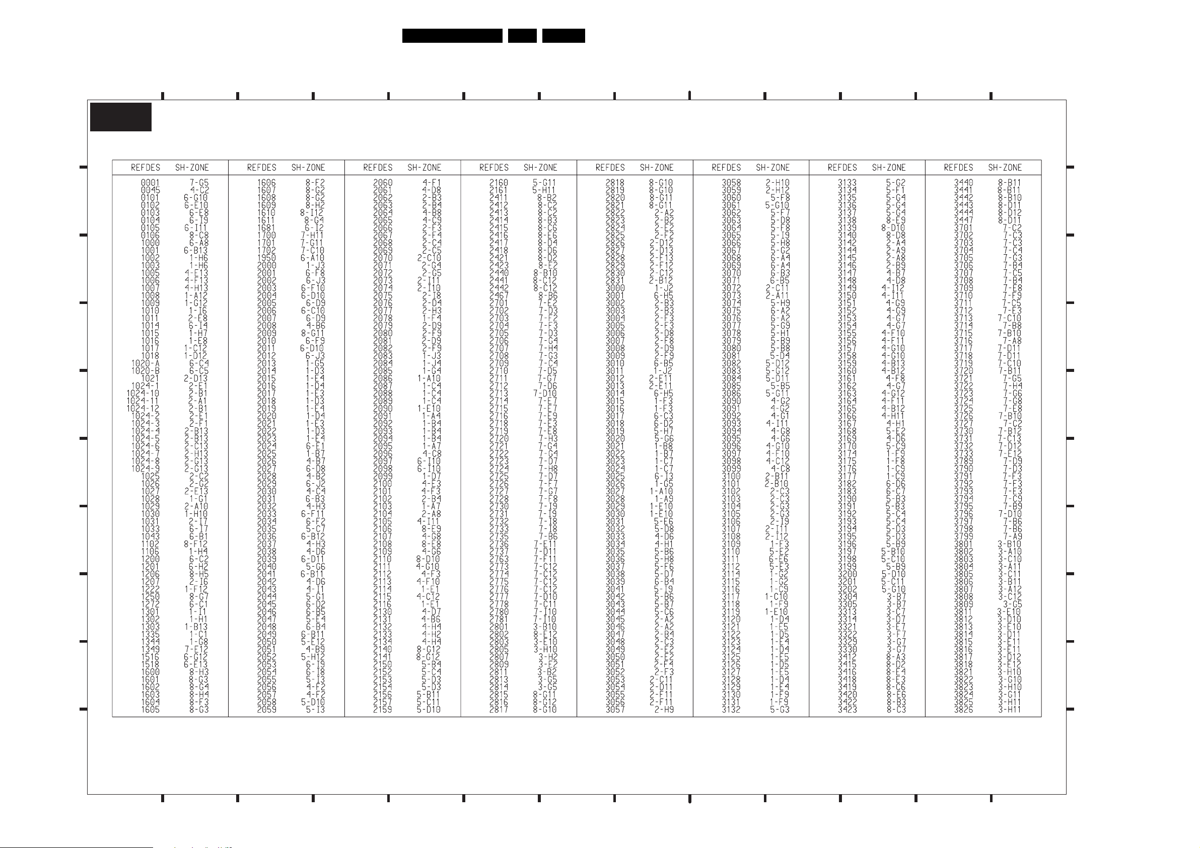
Circuit Diagrams and PWB Layouts
C10
Mapping SSM C1-C8 Part 1
39DPTV465 7.
A
B
C
D
11
C10
SMALL SIGNAL MODULE (AP)
54321
6
7
12111098
13
A
B
C
D
E
F
H
E
F
G
H
I
I
J
3135 033 3345.7
1
65432 1312111098
7
E_15000_020.eps
061004
J
Page 40
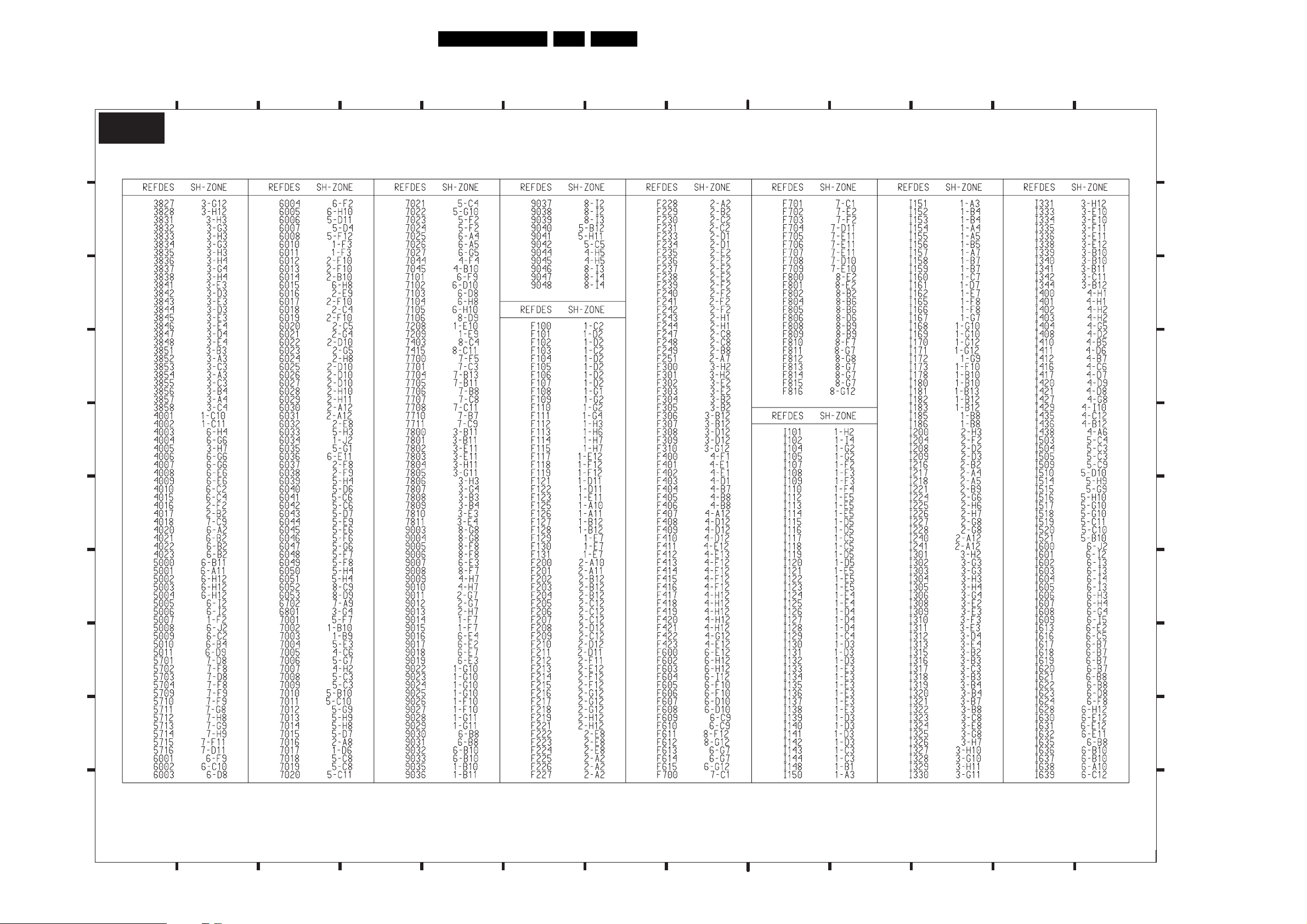
Circuit Diagrams and PWB Layouts
C11
Mapping SSM C1-C8 Part 2
40DPTV465 7.
A
B
C
D
11
C11
SMALL SIGNAL MODULE (AP)
6
7
12111098
1354321
A
B
C
D
G
E
H
E
F
I
F
G
H
I
J
3135 033 3345.7
1
5432 1312111098
6
7
E_15000_021.eps
061004
J
Page 41
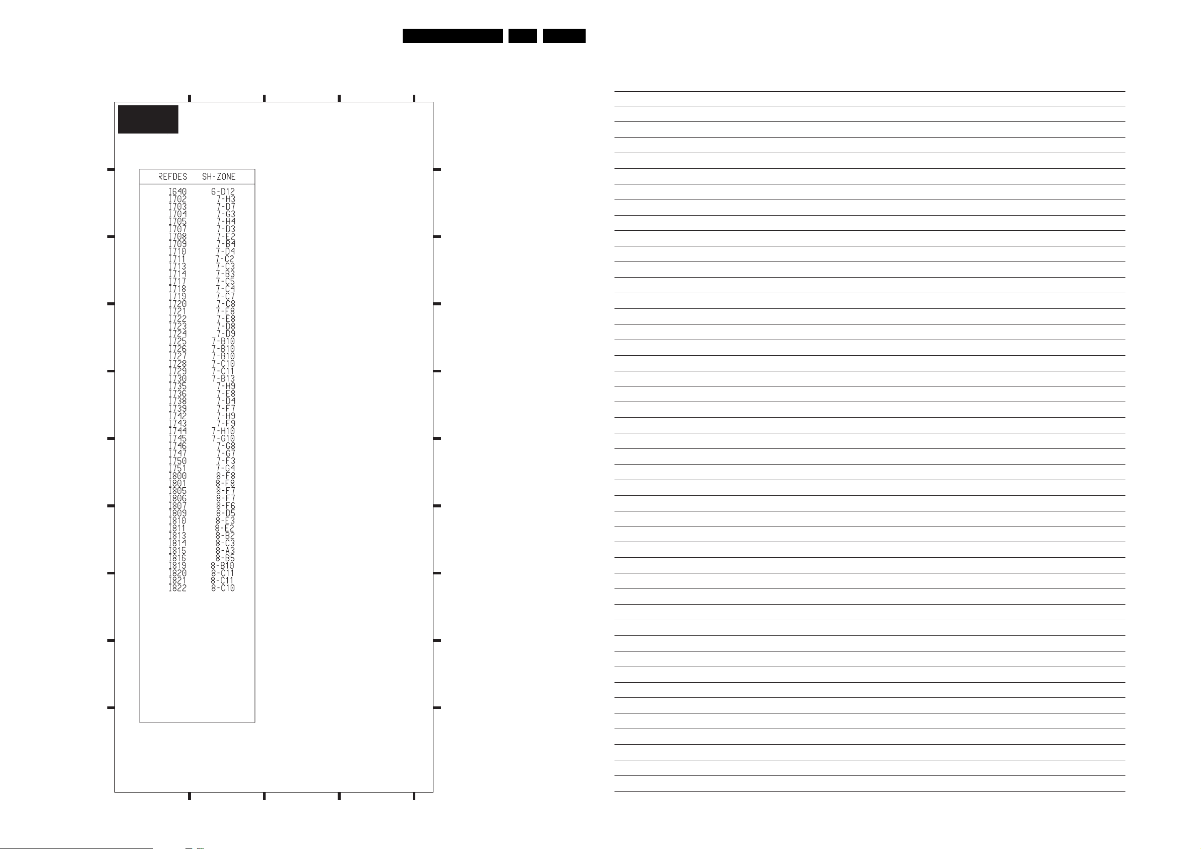
Circuit Diagrams and PWB Layouts
C12
Mapping SSM C1-C8 Part 3
41DPTV465 7.
Personal Notes:
4321
A
B
C
D
11
C12
SMALL SIGNAL MODULE (AP)
A
B
C
D
E
G
H
E
F
F
G
H
I
I
J
3135 033 3345.7
143
J
E_15000_022.eps
191004
E_06532_012.eps
131004
2
Page 42
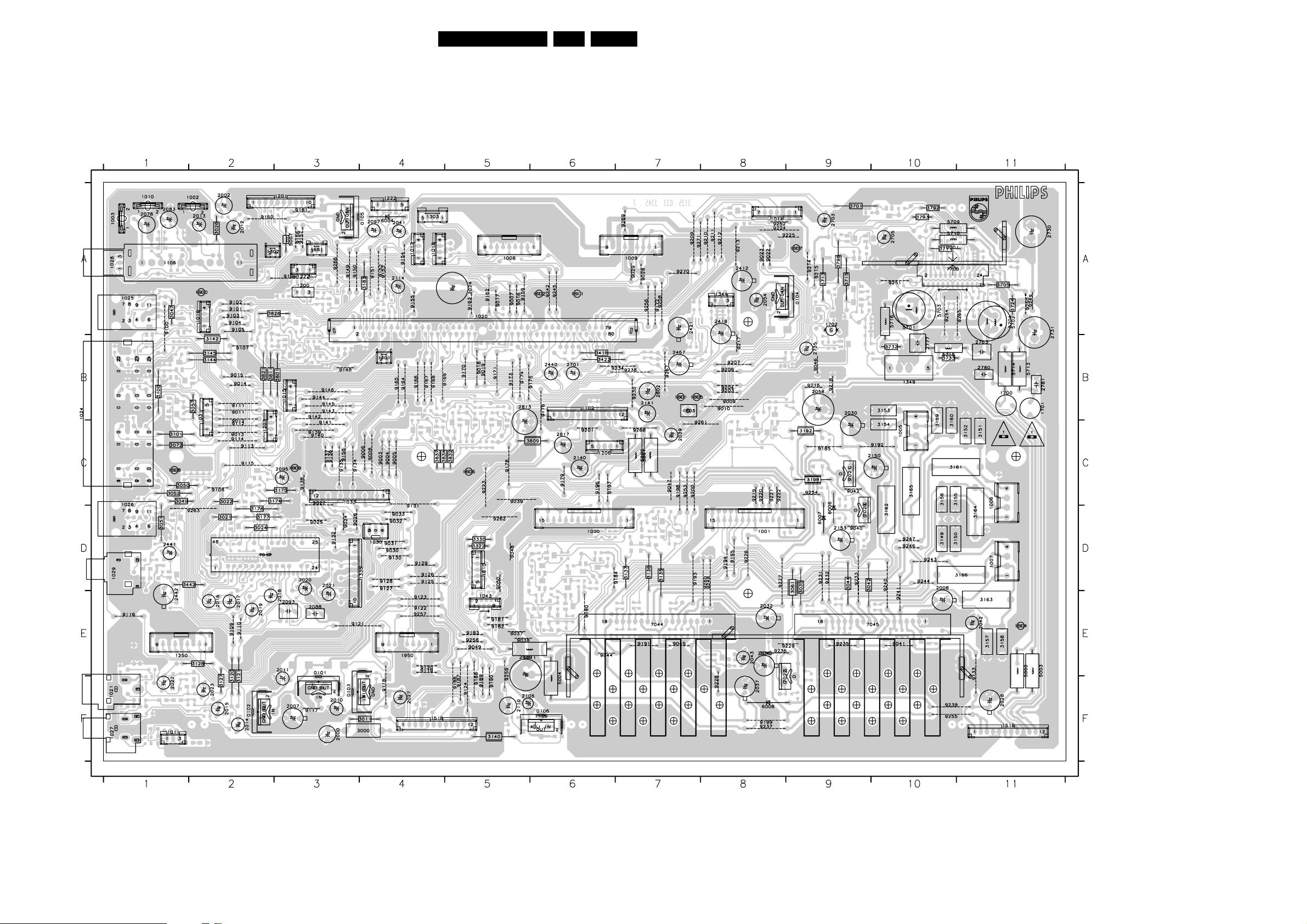
Layout SSM (Top Side)
0001 A10
0045 E8
0101 E3
0102 F2
0103 F3
0104 A9
0105 A4
0106 F6
1000 D6
3135 033 3345.7
1001 D8
1002 A2
1003 A1
1005 C10
1006 C11
1007 D11
1008 A5
1009 A7
1010 A1
1011 F1
1014 A8
1015 B3
1016 A2
1017 A4
1018 A4
1020 A5
1021 F1
1025 A1
1026 C1
1027 F1
1028 A1
1029 D1
1030 D4
1031 B2
1033 C3
1043 E5
1102 B6
Circuit Diagrams and PWB Layouts
1106 A1
1200 A3
1201 A3
1206 C6
1207 C2
1222 A4
1250 E1
1272 A3
1301 B4
1302 A2
1303 A4
1335 D4
1344 A8
1349 B10
1516 F11
1518 F4
1600 A2
1601 B7
1602 A6
1603 B7
1604 E11
1605 B7
1606 C5
1607 A9
1608 C1
1609 C3
1610 D5
1611 A6
1681 A3
1700 B11
1701 B11
1702 A9
1950 E4
2000 F3
2002 A2
2007 F3
2008 D10
2010 F3
2011 E3
2012 A2
2013 A2
2014 F2
2015 F2
2016 E2
2017 E2
2018 E3
2019 E2
2020 D3
2021 D3
2022 F1
2023 F2
2024 A5
2027 F4
2028 F11
2030 B9
2032 E8
2037 F8
2038 E8
2039 C7
2041 A4
2042 E11
2043 E8
2054 A8
2058 B9
2059 E5
2078 A1
2083 A1
2088 E3
2093 E3
2095 C3
2097 A4
2106 F5
2110 F5
2114 A4
2140 C6
2141 B7
2150 C10
2153 D9
2412 A8
2418 A8
2421 A7
2440 B6
2441 D1
2442 E1
2467 B7
2701 B6
2703 A9
2705 A10
2730 A11
2731 A11
42DPTV465 7.
2735 B9
2763 B11
2777 B10
2780 B11
2781 B11
2802 B7
2813 B5
2817 C6
3000 F4
3011 F4
3021 D2
3022 C2
3024 D2
3026 A2
3035 D9
3042 D9
3044 D9
3047 A1
3049 C1
3050 C1
3051 D1
3052 C1
3057 B2
3061 D9
3072 C1
3100 B1
3101 C1
3120 F2
3121 F2
3127 F2
3128 E2
3135 D7
3136 D7
3137 D7
3140 F5
3142 B2
3144 B2
3145 B2
3149 D10
3150 D10
3151 C11
3152 C11
3153 B10
3154 C10
3155 C10
3156 C10
3157 E11
3158 E11
3159 C10
3160 C10
3161 C10
3162 D10
3163 E11
3164 D11
3165 C10
3166 D11
3174 C3
3175 C3
3176 D2
3177 D2
3183 A4
3192 C9
3198 C9
3322 D5
3330 D5
3418 B6
3422 B6
3442 D2
3701 A9
3705 A11
3711 A10
3713 A9
3715 A9
3724 A11
3732 B10
3733 B10
3792 A10
3793 A10
3798 A9
3801 B3
3809 C6
3811 B2
3821 B2
3826 A2
3832 C5
3834 C4
3837 C4
5000 C7
5001 C7
5002 E11
5003 E11
5004 F6
5007 A3
5011 E5
5701 A10
5702 A11
5703 A10
5704 A11
5709 A10
5710 A10
5713 B11
5714 B11
5715 B10
5716 A10
6004 A4
6006 D9
6007 D9
6008 F8
E_15000_023.eps
121004
7017 D2
7020 D9
7021 C9
7022 F8
7044 E7
7045 E10
7101 F3
7102 F2
7103 F4
7104 A8
7105 A3
7106 F6
7700 A10
9003 C4
9004 C4
9005 C4
9006 C4
9007 A5
9008 C4
9009 B8
9010 B8
9011 B2
9012 C2
9013 C2
9014 B2
9015 B2
9016 A5
9017 A5
9018 B5
9019 B5
9022 A8
9023 A8
9024 D3
9025 D3
9026 D3
9027 C3
9028 A7
9029 A7
9030 D4
9031 D4
9032 D4
9033 D4
9037 E5
9038 E5
9039 C5
9040 D9
9041 E10
9042 C9
9044 E6
9045 E7
9046 B9
9047 C7
9048 D5
9049 E5
9050 D5
9100 A1
9101 A2
9102 A2
9103 A2
9104 A2
9105 A2
9106 A3
9107 B2
9108 C2
9109 E2
9110 E2
9111 B2
9112 C2
9113 C2
9114 C2
9115 C2
9116 E1
9117 F3
9118 F4
9119 E4
9120 E4
9121 E3
9122 E4
9123 E4
9124 F5
9125 D4
9126 D4
9127 D4
9128 D4
9129 D4
9130 D4
9131 D4
9132 D3
9133 E11
9134 C3
9135 C3
9136 C3
9137 C3
9138 C3
9139 C3
9140 C3
9141 C3
9142 B3
9143 B3
9144 B3
9145 B3
9146 B3
9148 B3
9149 A3
9150 A3
9151 A4
9152 A4
9153 A4
9154 A4
9155 A4
9156 A3
9157 A3
9158 C3
9159 A5
9160 A2
9161 A3
9162 A5
9163 A5
9164 B4
9165 B4
9166 B4
9167 B4
9168 B4
9169 B4
9170 B5
9171 B5
9172 A7
9173 B5
9174 B5
9175 B6
9176 B6
9178 C5
9179 C6
9180 E6
9181 E5
9182 E5
9183 E5
9184 D7
9185 C9
9186 F5
9187 F5
9188 F5
9189 F5
9190 F5
9191 E7
9192 C10
9193 D7
9194 D8
9195 D8
9196 C6
9197 C6
9198 C7
9199 F8
9200 C7
9201 C6
9203 B8
9204 B8
9206 B8
9207 B8
9208 A7
9209 A7
9210 A8
9211 A8
9212 A8
9213 A8
9214 A9
9215 A9
9216 B9
9217 B8
9218 B9
9219 C8
9220 C8
9221 C8
9222 C8
9223 C5
9224 A8
9225 A9
9226 D8
9227 D8
9228 F8
9229 E9
9230 B7
9231 D9
9232 D9
9233 D9
9234 B7
9235 E9
9236 E8
9237 F8
9238 B7
9239 F10
9240 D10
9241 E10
9242 A6
9243 D10
9244 D10
9245 A6
9246 D10
9247 D10
9248 D8
9249 A11
9250 A11
9251 A10
9252 A8
9253 C7
9254 C9
9255 F10
9256 A7
9257 E4
9258 E5
9259 E5
9260 D8
9261 C8
9262 D5
9263 D2
9264 A10
9265 A11
9266 A3
9267 B7
9268 C7
9269 A7
9270 A7
9271 A7
Page 43
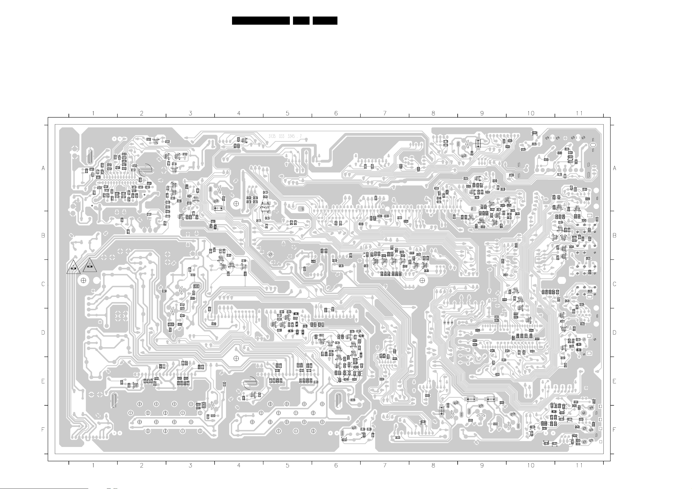
Layout SSM (Bottom Side)
2001 F9
2003 F9
2004 E9
2005 E8
2006 E8
2009 C5
2025 D10
2026 E2
2029 A10
2031 A8
2033 F7
2034 A7
2035 E6
2036 D3
2040 E6
2044 D5
2045 A9
2046 A9
2047 C3
2048 A8
2049 D3
2050 D3
2051 E2
2052 E3
2053 A4
2055 E6
2056 E5
2057 E5
2060 E5
2061 E3
2062 B11
2063 B11
2064 E3
2065 E3
2066 C10
2067 C10
2068 A11
2069 A10
2070 B11
2071 C11
2072 D11
2073 B11
2074 B11
2075 B11
2076 A10
2077 D11
2079 F10
2080 F10
2081 F11
2082 F10
2084 A11
2085 A10
2086 D10
2087 D10
2089 D9
2090 D10
2091 D10
2092 D10
2094 D9
2096 E3
2098 A9
2099 D10
2100 E5
2101 E5
2102 C11
2103 D10
2104 B11
2105 E5
2107 E5
2108 F7
2109 E5
2111 E2
2112 E5
2113 E3
2115 E3
2116 A10
2130 E2
2131 E2
2132 E5
2133 E5
2134 E6
2152 C3
2154 D6
2156 C2
2157 C3
Circuit Diagrams and PWB Layouts
2159 D3
2160 F3
2161 E4
2411 B6
2413 A5
2414 B5
2415 A4
2416 A4
2417 B4
2423 B6
2702 A2
2704 A1
2706 A2
2707 A1
2708 A1
2709 A2
2710 A2
2711 A1
2712 A2
2713 A3
2714 A2
2715 A2
2716 A2
2718 A2
2719 A2
2720 A1
2721 A1
2722 A1
2723 A2
2724 A1
2725 A2
2726 A1
2727 A1
2728 A1
2732 A1
2733 A1
2736 B2
2737 B2
2773 B3
2774 B3
2775 A3
2776 A3
2778 A3
2801 C9
2803 C9
2805 B10
2807 B8
2809 B8
2811 B7
2814 C7
2815 B6
2816 C6
2818 B6
2819 C6
2820 B6
2821 C6
2822 B11
2823 B11
2824 C11
2825 C11
2826 F11
2827 E11
2828 F11
2829 F11
2830 C11
2831 B11
3001 A4
3002 B11
3003 B11
3004 C10
3005 C10
3006 F11
3007 F11
3008 F11
3009 F10
3010 A9
3012 F11
3013 F11
3014 A4
3015 A11
3016 A11
3017 A9
3018 A9
3019 D6
3020 E6
3023 C9
3025 A10
3027 D10
3028 D10
3029 C10
3030 C10
3031 E7
3032 D6
3033 E2
3034 E4
3036 D6
3037 E6
3038 E6
3039 A9
3041 D6
3043 D6
3045 B11
3046 B11
3048 A11
3053 F11
3054 E11
3055 F11
3056 F10
3058 B11
3059 B11
3060 E6
3062 E6
3063 D6
3064 E6
3065 D6
3066 D6
3067 D5
3068 A9
3069 A9
3070 A9
3071 A9
3073 D11
3074 D6
3075 D7
3076 D7
3077 D6
3078 D5
3079 D6
3080 D6
3081 C3
3082 D3
3083 E3
3084 D3
3085 C3
3086 F3
3090 E5
3091 E5
3092 E5
3093 E5
3094 E5
3095 E5
3096 E2
3097 E3
3098 E3
3099 E3
3102 A11
3103 A11
3104 C11
3105 D11
3106 B11
3107 B11
3108 B11
3109 A11
43DPTV465 7.
3110 D5
3111 B7
3112 D5
3114 A11
3115 A11
3116 A7
3117 A7
3118 A8
3119 A8
3122 D10
3123 D10
3124 D10
3125 E9
3126 D9
3129 D9
3130 D9
3131 D9
3132 D5
3133 D5
3134 D5
3138 F7
3139 F7
3146 B11
3147 E2
3148 E3
3167 E4
3168 D5
3169 E2
3170 D6
3182 B8
3190 B3
3191 B4
3193 C3
3194 B3
3195 C4
3196 B4
3197 B4
3199 C4
3200 C4
3201 D3
3202 F3
3304 E7
3305 D6
3313 D7
3314 D6
3321 D7
3329 E7
3412 B5
3415 B5
3416 B5
3419 A4
3420 A4
3423 A5
3440 E11
3441 E11
3443 D11
3444 D11
3447 D11
3702 A2
3703 A2
3704 A2
3706 A2
3707 A2
3708 A2
3709 A2
3710 A2
3712 A2
3714 A3
3716 A3
3717 B2
3718 B2
3719 B3
3720 B3
3721 A1
3722 A1
3723 A1
3725 A1
3726 B3
3727 A3
3730 A3
3731 A3
3789 A3
3790 A2
3791 A1
3794 B3
3795 B3
3796 A3
3797 A3
3799 B3
3802 B9
3803 B9
3804 B9
3805 B9
3806 B9
3807 B9
3808 B9
3812 B9
3813 B9
3814 A9
3815 B10
3816 B9
3817 A9
3818 B10
3822 B10
3823 A10
3824 A9
3825 A10
3827 A9
3828 A9
3831 B8
3833 C8
3835 B8
3836 C8
3838 B8
3841 B7
3842 C7
3843 B7
3844 C7
3845 B7
3846 B7
3847 C7
3848 C7
3851 B7
3852 C7
3853 B7
3854 C7
3855 B7
3856 B7
3857 C7
3858 B7
4001 A7
4002 A8
4003 A4
4004 B7
4005 B7
4006 B7
4007 B7
4008 B7
4009 B7
4010 A9
4011 D11
4012 E9
4013 E9
4014 A11
4015 A8
4016 C11
4017 A11
4018 A3
4020 D6
4021 D6
4022 D5
4023 D6
4024 A3
5005 A10
5006 A9
5008 A10
5009 A9
5010 A8
5711 A1
5712 A1
6001 E9
6002 E9
6003 F8
6005 A9
6010 A11
6011 A11
6012 F10
6013 F10
6014 B10
6015 A4
6016 F11
6017 F11
6018 A11
6019 F11
6020 A11
6021 D11
6022 F11
6023 D11
6024 B11
6025 F11
6026 F10
6027 F10
6028 B11
6029 B11
6030 D11
6031 D11
6032 F11
6033 D5
6034 A10
6035 D5
6036 F8
6037 F10
6038 F10
6039 D5
6040 E6
6041 E6
6042 E6
6043 D7
6044 D7
6045 E6
6046 E6
6047 E6
6048 E6
6049 E6
6050 D5
6051 D5
6052 F6
6053 F7
6702 B4
6801 B7
7001 E6
7002 C10
7003 D10
7004 D5
7005 E2
7006 E6
7007 E4
7008 C4
7009 B4
7010 C4
7011 C4
7012 D6
7013 D6
7014 D6
7015 D6
7016 B11
7018 D6
7019 D6
7023 D5
7024 D5
7025 A9
7026 A9
7027 A4
7208 C10
7209 C10
7403 A5
7415 D11
7701 A2
7704 A3
7705 A3
7706 A3
7707 A3
7708 B3
7710 A3
7711 A3
7800 B9
7801 B9
7802 B9
7803 B9
7804 A10
7805 A9
7806 C8
7807 C8
7808 C7
7809 C7
7810 C7
7811 C7
9035 A8
9036 A8
3135 033 3345.7
E_15000_024.eps
121004
Page 44
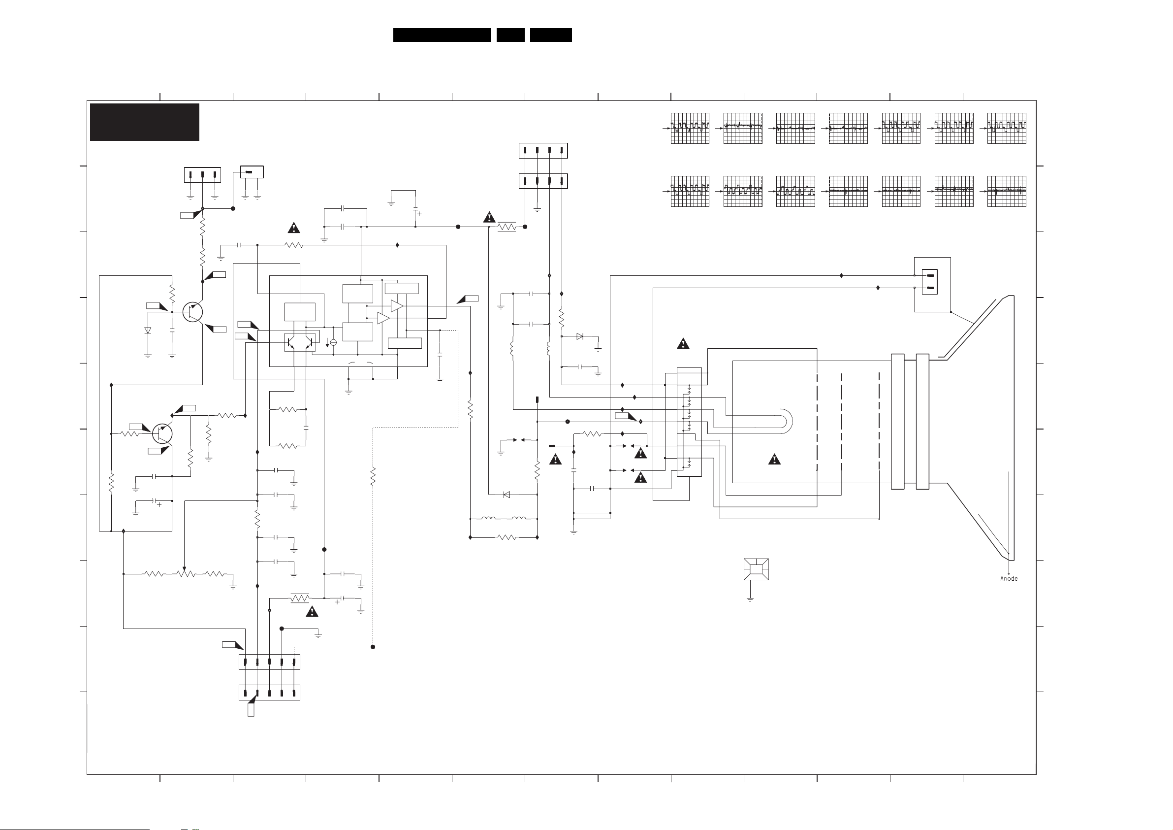
CRT Panel: Red
D(R)1
Circuit Diagrams and PWB Layouts
44DPTV465 7.
D(R)1
A
B
C
D
I103
E
F
3213
G
H
I
J
100R
680R
I133
3208
RV5
RV3
BAS216
4V
RV11
2209
1n
100u
2211
3225
2K2
6204
6K8
2201
I105
.5V
3.3V
7202
BF570
8.1V
21
3
RED CRT PANEL
To HOP Panel
12 3
I104
RV1
I112
3203
4V
100n
RV6
3223
3226
470R
1210
EH-S
3201
3200
1K5
-.7V
22R
75R
-.1V
7200
BF570
3209
3227
2K2
RV2
RV4
330R
3204
100R
RV10
1217
EH-B
1207
EH-S
1211
TMPJ02X-A1
1
F104
2219
2p2
RV13
RV7
I123
8.1V
1
1
N/U
23
2.2V
4V
3.2V
I114
3214
I134
.3V
2
2
RV12
5 IIN
4 VIN+
2 VIN-
2204
1n
2207
1u
N/U
100R
2212
1n
2215
1u
I135
11.6V
3
3
F103
4
3212
22K
11.2V
6
VCC
MIRROR
1X
RC+
RC-
3
1
3.3V
2.5V
3224
1K
10p
2210
3215
680R
3216
10R
4
5
4
5
To Green CRT Panel 1217
2224
47n
2214
47n
VDD
MIRROR
CURRENT
INPUT
911
F106
2213
1n
100u
2216
SLV
4
4
I106
3202
F125
1
7
To LSP Panel
1K5
6200
BYD33M
2218
100p
129V
3210
10K
I128
1n
2206
2208
100p
N/U
RV9
I117
I121
I127
1205
DSP
1206
DSP
I118
I125
-18V
6.2V
RV1 RV3RV2 RV6RV5RV4RV3
200mV / div AC
10µs / div
1V / div AC
10µs / div
1203
HPS0521
4
5
6
7
8
9
10
11
12
1
100mV / div AC
10µs / div
50V / div AC
10µs / div
5986
1202
EH-S
1
2
3
EH-B
1212
1
2
F102
2221
100n
2200
1n
RT-01T
1208
1
3218
3
6.2V
I107
5201
1204
220R
206V
4u7
2217
F117
I102
206V
10
4X
NC
3220
CASCODE
CASCODE
N/U
100R
7201
TDA6120Q
GND
8
128V
12OUTC
13OUT
7OUTM
21.5V
2203
RV8
129V
100p
3206
I119 I113
I115
47R
5202
0u47
3217
1R
6201
BAS21
3211
10K
5200
1209
DSP
5203
0u47
0001
HEATSINK
12
10
100mV / div AC
10µs / div
RV9 RV10RV8RV7 RV11 RV12
50V / div AC
10µs / div
3
11
100mV / div AC
10µs / div
100mV / div AC
10µs / div
I111
1V / div AC
10µs / div
100mV / div AC
10µs / div
I108
12
1
2
1201
1V / div AC
10µs / div
100mV / div AC
10µs / div
VH
13
1V / div AC
10µs / div
RV13
100mV / div AC
10µs / div
A
B
C
D
E
F
G
H
F105
NOTES
1. CAPACITANCE VALUES ARE IN FARADS:
m=MILI u=MICRO n=NANO p=PICO f=FEMTO
2. RESISTANCE VALUES ARE IN OHMS:
R=OHM K=KILO M=MEGA G=GIGA T=TERA
3. SAFETY TRIANGE REPRESENTS PCEC REPLACEMENT PART ONLY.
4. FOR VALUE SEE TABLE.
*
I
J
3135 013 3267.4
1 765
E_15000_008.eps
2 13
43 9
8
10
11
12
131004
Page 45
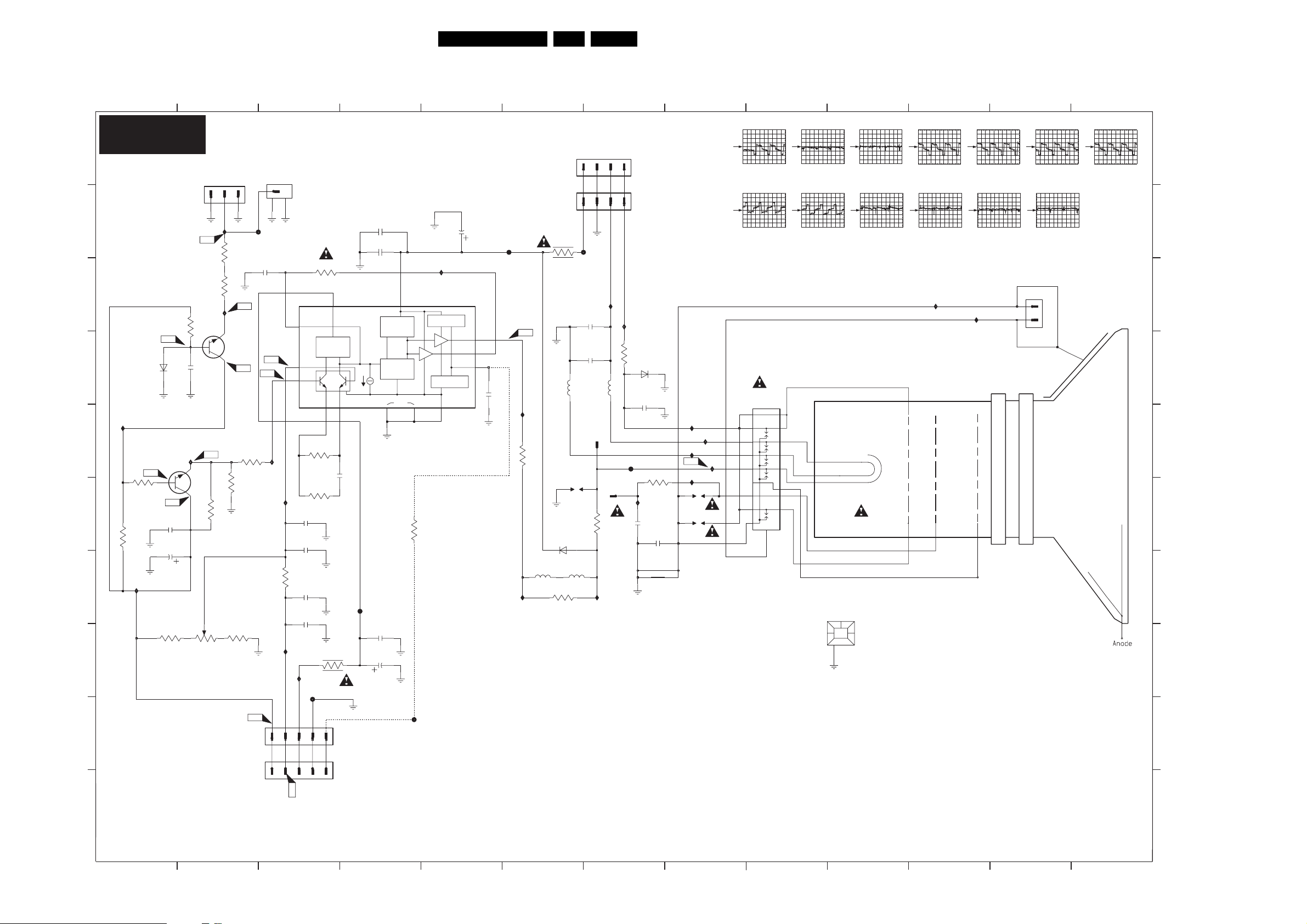
CRT Panel: Green
D(G)1
Circuit Diagrams and PWB Layouts
45DPTV465 7.
D(G)1
A
B
C
D
E
F
G
H
I
J
I103
3213
680R
I133
3208
100R
GV5
GV3
BAS216
4V
GV11
2209
1n
100u
2211
3225
2K2
To HOP Panel 1720
GV1
6K8
3203
.5V
6204
100n
2201
I105
3.3V
7202
BF570
8.1V
470R
21
3
4
GREEN CRT PANEL
1210
EH-S
12 3
-.7V
I104
22R
3201
75R
3200
I112
-.1V
7200
BF570
4V
GV6
3209
1K5
3223
3226
3227
2K2
GV4
GV2
330R
3204
100R
GV10
1217
EH-B
1207
EH-S
1211
TMPJ02X-A1
1
23
F104
2219
2p2
GV13
GV7
I123
I114
8.1V
1
1
3214
.3V
2
2
2.2V
N/U
4V
3.2V
I134
5 IIN
4 VIN+
2 VIN-
2204
1n
2207
1u
N/U
100R
2212
1n
2215
1u
I135
11.6V
3
3
GV12
3212
22K
11.2V
6
VCC
MIRROR
1X
RC+
RC-
3
1
3.3V
2.5V
3224
1K
2210
3215
680R
3216
10R
F103
To Red CRT Panel 1207
4
5
4
5
To HOP Panel 1701
10p
2224
47n
2214
47n
VDD
MIRROR
CURRENT
INPUT
911
F106
2213
1n
100u
2216
5986
1202
EH-S
1
2
3
EH-B
1212
1
2
F102
2221
100n
2200
1n
RT-01T
1208
1
3218
I107
3
5201
1204
SLV
220R
206V
4u7
2217
F117
I102
206V
10
4X
NC
3220
CASCODE
CASCODE
N/U
100R
7201
TDA6120Q
GND
8
128V
12OUTC
13OUT
21.5V
7OUTM
2203
GV8
129V
100p
3206
I119 I113
I115
47R
5202
0u47
3217
1R
6201
BAS21
3211
10K
5200
1209
DSP
5203
0u47
7
To LSP Panel 1202
4
To Red CRT Panel 1202
4
6.2V
I106
1K5
3202
6200
BYD33M
2218
100p
F125
1
I128
1n
2206
129V
3210
10K
2208
100p
N/U
I117
I121
GV9
I127
1205
DSP
1206
DSP
I118
I125
GV1 GV3
200mV / div AC
10µs / div
50V / div AC
10µs / div
1203
HPS0521
4
-18V
6.2V
5
6
7
8
9
10
11
12
1
GV2
100mV / div AC
10µs / div
50V / div AC
10µs / div
10
100mV / div AC
10µs / div
GV10 GV11GV9GV8 GV12 GV13
100mV / div AC
10µs / div
0001
HEATSINK
3
12
11
1V / div AC
10µs / div
100mV / div AC
10µs / div
I111
1V / div AC
10µs / div
100mV / div AC
10µs / div
I108
12
GV6GV5GV4
100mV / div AC
1201
1
2
1V / div AC
10µs / div
10µs / div
VH
13
GV7
1V / div AC
10µs / div
A
B
C
D
E
F
G
H
F105
NOTES
1. CAPACITANCE VALUES ARE IN FARADS:
m=MILI u=MICRO n=NANO p=PICO f=FEMTO
2. RESISTANCE VALUES ARE IN OHMS:
R=OHM K=KILO M=MEGA G=GIGA T=TERA
3. SAFETY TRIANGE REPRESENTS PCEC REPLACEMENT PART ONLY.
4. FOR VALUE SEE TABLE.
*
I
J
3135 013 3267.4
1 765
E_15000_007.eps
2 13
43 9
8
10
11
12
131004
Page 46
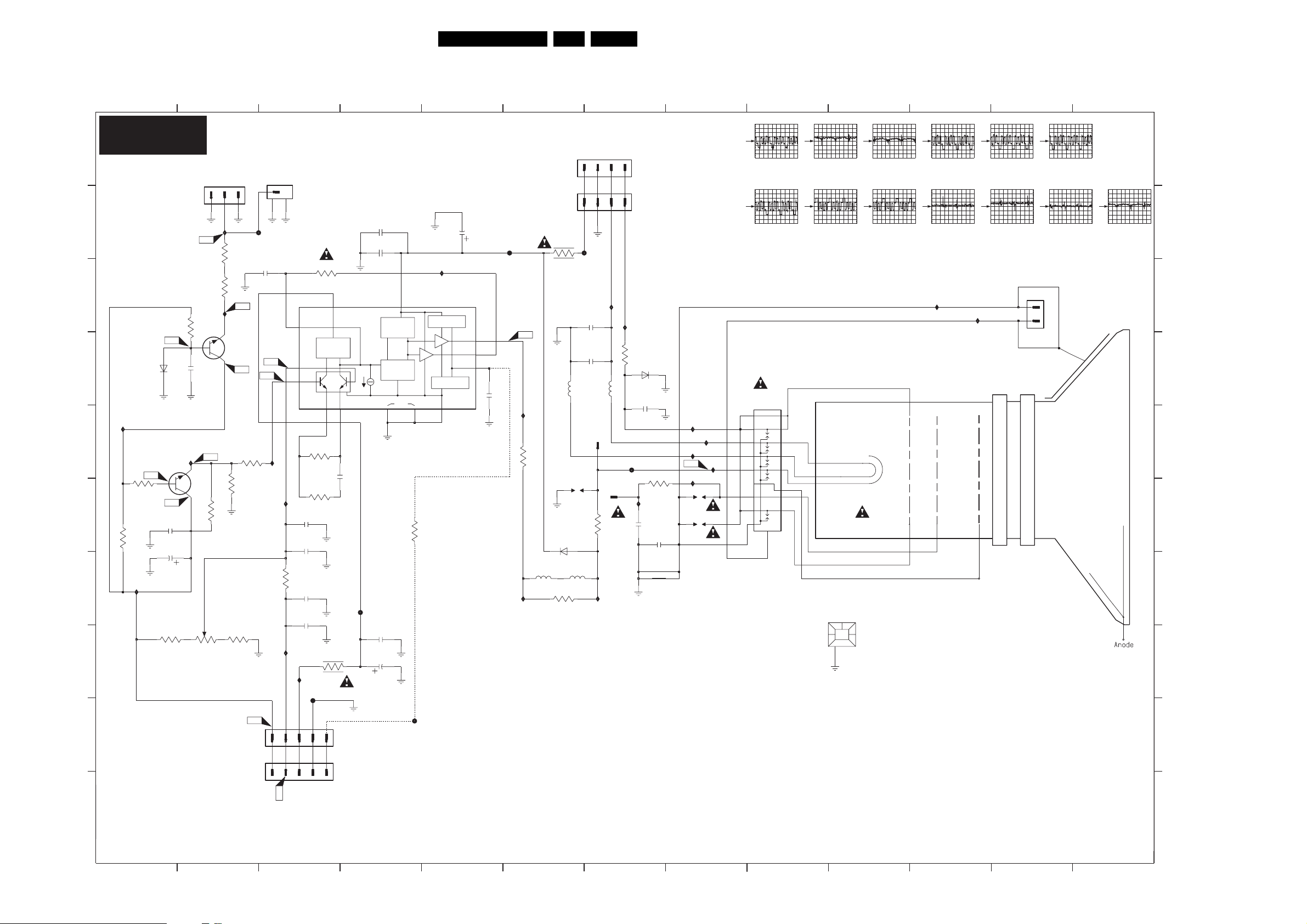
CRT Panel: Blue
D(B)1
Circuit Diagrams and PWB Layouts
46DPTV465 7.
D(B)1
A
B
C
D
E
F
G
H
I
J
I103
3213
680R
I133
3208
100R
BV5
BV3
BAS216
4.1V
BV11
2209
1n
100u
2211
3225
2K2
To HOP Panel 1720
12 3
BV1
6K8
3203
.5V
6204
100n
2201
I105
BV6
3.3V
7202
BF570
8.1V
3223
470R
21
3
BLUE CRT PANEL
I104
I112
4.1V
3226
1210
EH-S
3201
3200
1K5
-.6V
-.1V
7200
BF570
3209
3227
22R
75R
2K2
BV4
BV2
330R
3204
100R
BV10
1217
EH-B
1207
EH-S
1211
TMPJ02X-A1
1
F104
2219
2p2
BV13
BV7
I123
I114
8.1V
1
1
N/U
23
5 IIN
2.2V
4 VIN+
4V
2 VIN-
3.2V
2204
1n
2207
1u
N/U
3214
100R
2212
1n
2215
1u
I134
I135
F103
.3V
11.6V
2
3
3
2
To HOP Panel 1701
BV12
3212
22K
11.2V
6
VCC
MIRROR
1X
RC+
RC-
3
1
3.3V
2.5V
3224
1K
10p
2210
3215
680R
3216
10R
To Green CRT Panel 1207
4
5
4
5
4
2224
47n
2214
47n
206V
10
VDD
MIRROR
4X
CURRENT
INPUT
NC
911
3220
100R
F106
2213
1n
100u
2216
F105
5986
4u7
2217
I102
7201
TDA6120Q
CASCODE
12OUTC
13OUT
7OUTM
CASCODE
GND
8
N/U
21.5V
2203
F117
123V
BV8
124V
100p
I115
47R
3206
BAS21
5202
0u47
I119 I113
EH-B
1212
3217
1R
6201
3211
10K
5200
206V
1209
DSP
5203
0u47
1
1
F102
2221
100n
2200
1n
RT-01T
2
2
1208
1
3218
1202
EH-S
I107
3
3
6.2V
5201
1204
SLV
220R
7
To LSP Panel 1202
4
To Green CRT Panel 1202
4
I106
1K5
3202
6200
BYD33M
2218
1
F125
2206
100p
124.3V
3210
I128
1n
2208
100p
I117
I121
BV9
I127
10K
N/U
1205
DSP
1206
DSP
I118
-18V
I125
6.2V
BV1
200mV / div AC
10µs / div
BV7
1V / div AC
10µs / div
1203
HPS0521
4
5
6
7
8
9
10
11
12
100mV / div AC
10µs / div
50V / div AC
10µs / div
1
0001
HEATSINK
12
10
3
BV3BV2
100mV / div AC
10µs / div
50V / div AC
10µs / div
11
BV5BV4
1V / div AC
10µs / div
BV10 BV11BV9BV8 BV12 BV13
100mV / div AC
10µs / div
I111
100mV / div AC
I108
1V / div AC
10µs / div
10µs / div
12
1
2
1201
BV6
1V / div AC
10µs / div
100mV / div AC
10µs / div
VH
NOTES
1. CAPACITANCE VALUES ARE IN FARADS:
m=MILI u=MICRO n=NANO p=PICO f=FEMTO
2. RESISTANCE VALUES ARE IN OHMS:
R=OHM K=KILO M=MEGA G=GIGA T=TERA
13
100mV / div AC
10µs / div
A
B
C
D
E
F
G
H
I
3. SAFETY TRIANGE REPRESENTS PCEC REPLACEMENT PART ONLY.
4. FOR VALUE SEE TABLE.
*
J
3135 013 3267.4
1 765
E_15000_006.eps
2 13
43 9
8
10
11
12
131004
Page 47
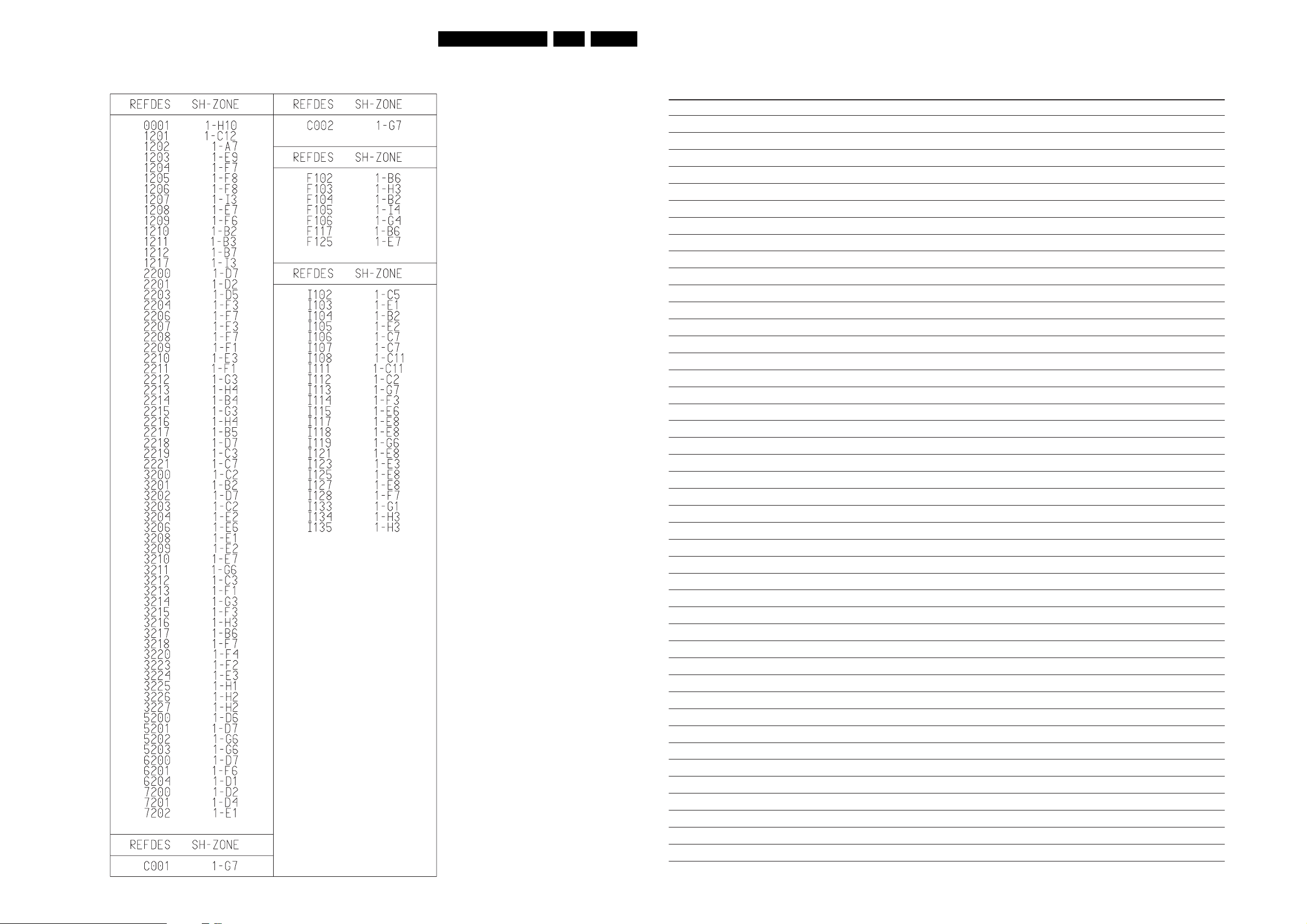
Circuit Diagrams and PWB Layouts
Mapping CRT Panel: Red, Green, and Blue
47DPTV465 7.
Personal Notes:
E150000_135.eps
191004
E_06532_012.eps
131004
Page 48
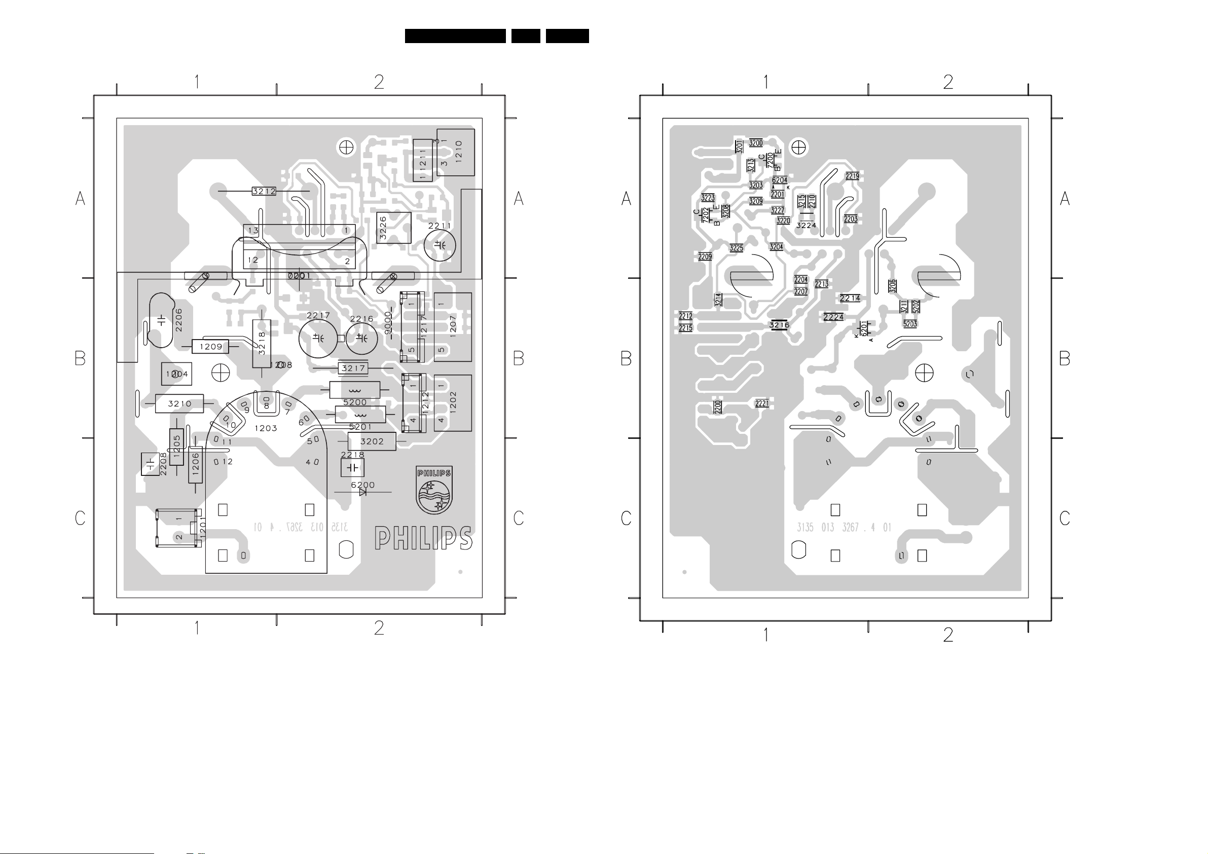
Circuit Diagrams and PWB Layouts
48DPTV465 7.
Layout CRT Panel (Top Side)
0001 A2
1201 C1
1202 B2
1203 B1
1204 B1
1205 C1
1206 C1
1207 B2
1208 B2
1209 B1
1210 A2
1211 A2
1212 B2
1217 B2
2206 B1
2208 C1
2211 A2
2216 B2
2217 B2
2218 C2
3202 C2
3210 B1
3212 A1
3217 B2
3218 B1
3226 A2
5200 B2
5201 B2
6200 C2
7201 A2
9000 B2
Layout CRT Panel (Bottom Side)
2200 B1
2201 A1
2203 A1
2204 B1
2207 B1
2209 A1
2210 A1
2212 B1
2213 B1
2214 B1
2215 B1
2219 A1
2221 B1
2224 B1
3200 A1
3201 A1
3203 A1
3204 A1
3206 B2
3208 A1
3209 A1
3211 B2
3213 A1
3214 B1
3215 A1
3216 B1
3220 A1
3223 A1
3224 A1
3225 A1
3227 A1
5202 B2
5203 B2
6201 B1
6204 A1
7200 A1
7202 A1
3135 013 3267.4
E_15000_009.eps
061004
3135 013 3267.4
E_15000_010.eps
061004
Page 49
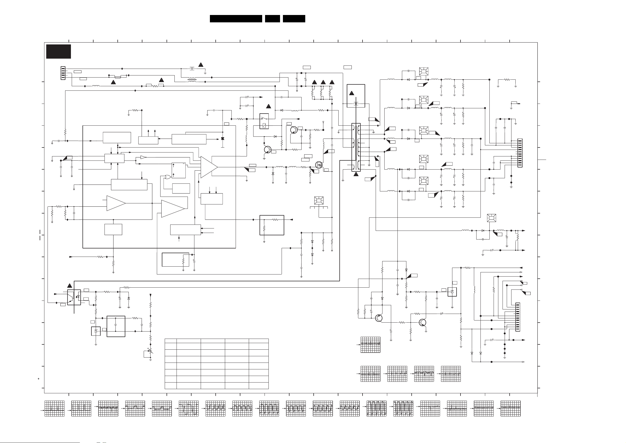
Large Signal Panel
E1
1
2
3
Circuit Diagrams and PWB Layouts
4
49DPTV465 7.
8
9
10 11
12
13
14
155
17
186 167
19
20
E1
1
A
B
C
D
E
F
G
H
I
J
K
L
M
N
O
2
To P ow er
Supply
Panel
1500
GND_C
GND_C
GND_C
VCC
56.5V
3
4
5
1500
B5P-VH
3314
2309
I135
82p
F106
680p
2310
GND_C
I143
3315
15K
1K0
3317
3316
I148
VCC
6
13.5V
5
4
19V
0V
I159
NOTES
1. CAPACITANCE VALUES ARE IN FARADS:
m=MILI u=MICRO n=NANO p=PICO f=FEMTO
2. RESISTANCE VALUES ARE IN OHMS:
R=OHM K=KILO M=MEGA G=GIGA T=TERA
3. SAFETY TRIANGE REPRESENTS PCEC REPLACEMENT PART ONLY.
4. FOR VALUE SEE TABLE.
*
3135 033 3425.3
1
F12
HDR2K4 LARGE SIGNAL PANEL (AP)
2390
2n2
5330
46
3
SUPPLY &
INITIALIZATION BLOCK
Q
Set
W8051
1
I110
GND_C
BUFFER
Vovp out
THERMAL
Vref
OVERVO LTAG E
MANAGEMENT
CONTROL
Iref
SS|DMAX|V_M
11
I149
2.4V
10K
1u0
3338
2306
GND_C
3135_037_12741_01
6
P10
GND_C
PEMG CH 4:3 PEMG CH 16:9
202002490682
470u 450V 470u 450V
NOT USED NOT USED NOT USED
NOT USED
NOT USED NOT USED
NOT USED
NOT USED
NOT USED NOT USED
3135_037_12751_01 3135_037_12761_01
202002490682
P11P9
82K
P7
220p
GND_C
GND_C
47K
13.5V
.24V
2.5V
1n0
L42
81.2V
8
9
2.5V
10
15
2353
12
14
2311
13
3.5V
7303
CQY80NG
152.4V
164V
I113
7302
MC44603AP
DEMAG_DET
SYNC_IN
CT
RF_SB
RP_SB
V_FB_IN
ERR_AMP_OUT
1
0V
2
19V
3
TL431BCLP
2
I164
I111
5315
I166
1300
5HT
I118
3313
10K
GND_C
3300
I114
22K
I132
16
2.5V
Vosc prot
Vosc
RREF
Vref Iref
REFERENCE
BLOCK
Vref
enable
Vdem in
Rref
DEMAGNETICATION
MANAGEMENT
Vdem out
Iref
OSCILLATOR
Latch
Iref
STANDBY
(REDUCED FREQUENCY)
Reset
SHUTDOWN
2.5V
ERROR
AMP
FOLDBACK
1.2V
5 FB_IN
I150
3318
150K
I157
0V
20V
4K7
3326
I158
3327
100R
0V
18.9V
1
K
R
7304
A
2
P7
I160
3
18.8V
3328
100R
0V
RESERVED
3
15K
3319
GND_C
3371
3K3
I156
1u0
6330
2328
BZX79-C22
3325
47K
2n2
2333
4n7
2334
I161
1
4
P8 P12
+130VS
3324
100K
I188
47K
3350
2K7
3323
I162
3322
470R
23
5
CURRENT
SENSE
Dmax & SOFT-STAR T
.14V
7 CUR_SEN_IN
RESERVED
Ref Des
2300
2333
2337
2391
3320 NOT USED NOT USED
3321
3338
I165
2346
100n
Vcc
UVLO1
UVLO1
Vref
NOT USED
NOT USED
2354
47u 25V
2303
100u 25V
GND_C
3311
F107
4R7
3312
5303
I136
2
VC
13V
OUT
3
2.8V
4
GND
GND_C
13.5V
I130
1
0V
VCC
18V
Vcc
6
OVP
1.9V
PEMG AP 4:3
NOT USED NOT USED
202002490562
470u 400V
NOT USED
NOT USED
NOT USED
89
4
75R
BC547B
164V
P8
I146
NOT_USED
319801912220
2n2
NOT USED
202055490173
2n2
319801108220
8K2
319801108220
8K2
319802151030
10K
120V Mains = 152V to 166V 220V Mains = 233V to 316V
VCC
1305
G5PA-1-5VDC
23
1
6313
1N4148
I134
.8V
0V
7300
*
220V Mains = 233V to 316V
I139
6322
GND_C
3321
8K2
8K2
3320
RESERVED
GND_C
10
P13
F111
470u
2337
I163
470p
2302
6301
RGP15J
3304
.8V
1K0
I125
2300
F108
GND_C
5312
+5VSTDBY
0V
7309
BC547B
3303
100K
I128
.7V
.4V
10n
2349
120V Mains = 152V to 166V
I140
5301
5302
BZX55-C15
470p
GND_C
P14
3306
15R
2305
GND_C
VCC
I144
3310
4n7
2308
390R
2307
4n7
GND_C
I152
11
470u
3301
220R
220R
3307
4R7
1-J20
3344
15K
F117
15K
3343
5305
7301
STW13NB60
*
I141
3.4V
G
P9
10K
3305
0032
MECHPART
12345
6302
0R22
1N5062
I142
GND_C
6303
1N5062
GND_C
P15
0033
HEATSINK
470p
2323
5308
1u0
6308
BY229X-600
RESERVED
3365
3302
220R
2391
2n2
I116
I120
5300
P11
US54018
2n2
GND_C
330p
11 12
10
8
6
STANDBY
2301
2304
P10
D
S
0V
.1V
3309
0R22
GND_C
2
1
3308
3381
I115
13
AGND
14
15
16
17
18
19
20
21
22
P17
3380
100K
I119
I124
I127
P16
I129
1K0
2382
100p
6380
50V1u0
4K7
2384
BF423
7380
P23
500mV / div AC
10µs / div
I117
3390
RGP15J
I170
470p
2329
BY229X-600
5321
1u0
P12
5323
P13
I173
6309
2364
470p
BY229X-600
6316
P15
I174
5320
BY229X-600
2319
470p
5324
I137
BY229X-600
2361
470p
6318
2370
100p
I189
3358
100n
2371
3361
3382
100K
160V47u
2380
P24
6307
6317
RGP15J
18K
I190
4K7
3384
P26
18.2V
0V
3360
100R
3383
4K7
0V
-18.1V
P19
HEATSINK
0V
HEATSINK
0037
HEATSINK
HEATSINK
0V -37V
47K
12
I168
0041
12
I171
0045
12
35.9V
2
1
0V -22V
0047
2
1
3385
7381
BC547B
5317
5318
I169
10u
2324
1m0
1m0
AGND
P20
5316
5313
I172
10u
1m0
2330
AGND
P21
5322
I112
10u
1m0
2365
P23
5309
I133
10u
2320
1m0
5314
I138
P24
1K0
10u
2362
1m0
7305
TL431BCLP
I191
0V
3
R
2.6V
2372
100n
2381
100V2u2
AGND
2331
AGND
2366
2321
2363
1
1.8V
2
4K7
2327
3352
AGND
4K7
1m0
3353
AGND
4K7
1m0
2332
3354
4K7
1m0
3356
4K7
1m0
3357
I147
5306
I192
3359
68K
0V
K
A
6K8
3362
3K3
3363
6320
P27P26P25
F113
-18V
F114
18V
F115
100n
F118
F119
0039
HEATSINK
6305
MUR8100
2312
470p
10u
5336
F127
6321
1N4148
1N4148
2322
100n
12
I145
2314
470u
3347
F129
F132
2336
10u
F943
AGND
2326
3345
10R
1506
0-106451-1
1
2
F142
F141
AGND
100n
2325
100n
1516
B12B-EH-A
12
11
10
35V
-22V
100n
-37V
2335
5304
P27
2313
F121
F128
F125
10K
F134
F135
F136
F137
9
8
7
6
5
4
3
2
1
F140
F139
F120
4R7
3370
470u
+130VS
1-C12
+5VSTDBY
2-N19
F12
2-C20
2-D20
1518
B12B-EH-A
1
To SSM
2
Panel
3
4
1518
5
.8V
6
7
8
.3V
9
10
PWR FAIL
11
12
F131
PROTECT
2-J1
- AUDIO
+ AUDIO
+35V
- 22V
- 35V
+130VS
+130VHV
STANDBY
VBLANK
DEFGND
HBLANK
L42
+15V
To SSM
Panel
1516
A
B
C
D
E
F
G
H
I
J
K
L
M
N
O
500mV / div AC
10µs / div
127
P16
P17
14
20V / div AC
10µs / div
15
P18
5V / div AC
5ms / div
1613
P19
20V / div AC
10µs / div
17
P20
18
P21
19
P22
E_15000_025.eps
191004
20
2V / div AC
5ms / div
2V / div AC
10µs / div
5V / div AC
10µs / div
10V / div AC
5µs / div
10V / div AC
5µs / div
50V / div AC
5µs / div
20V / div AC
10µs / div
20V / div AC
10µs / div
20V / div AC
10µs / div
20V / div AC
10µs / div
20V / div AC
10µs / div
50V / div AC
10µs / div
50V / div AC
10µs / div
50V / div AC
10µs / div
5V / div AC
10µs / div
50V / div AC
10µs / div
1V / div AC
10µs / div
1V / div AC
10µs / div
Page 50
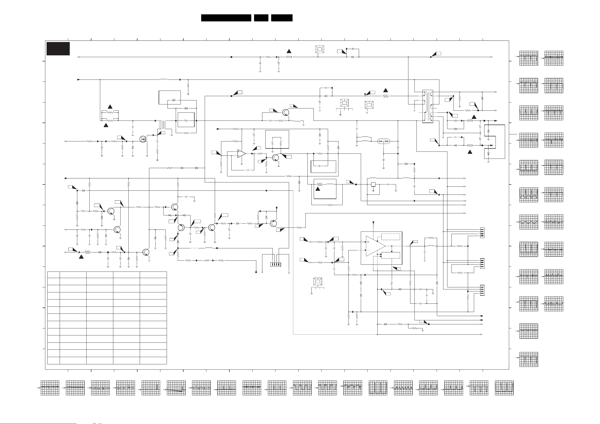
E2
Large Signal Panel
15
A
E2
B
C
D
E
F
G
H
I
J
NEG-HORIZ-PULSE
K
Ref Des
L
2817
2818
2833
M
2835
2849
3820
N
3822
3871
O
5807
6807
6808
P
6899
3135 033 3425.3
F2
HDR 2K4 LARGE SIGNAL PANEL (AP)
FILAMENT
+130VS
HOUT
3-K1
+15V
F9
I865
BZX284-C10
BZX284-C10
3842
PROTECT
1-N20
2838
L25
I882
2-A20
PEMG CH 4:3 PEMG CH 16:9
3135_037_12741_01 3135_037_12751_01
202055890484
560p 2KV
8n2 2KV
NOT USED
NOT USED
222237590343
319801211080
1R0 5% 1W
NOT USED
NOT USED
NOT USED
NOT USED
NOT USED
2 16
2-L10
6814
10K
1n0
6824
2837
3844
22K
3834
47R
470K
1u050V
I871
2839
3846
1R0
3
I842
2846
3841
F10
I866
3843
2K2
6815
1n0
22K
3845
6822
RGP15J
202055890484
222237590173
NOT USED
NOT USED
22237590343
15n 63015n 630
232219390342
1R5 1% 1W
NOT USED
NOT USED
NOT USED
NOT USEDNOT USED
3
Circuit Diagrams and PWB Layouts
4
5802
47u
RESERVED
3840
I840
-.4V
6829
330p
BAS216
F808
2840
3K3
3839
3K3
470R
.2V
BAS216
100K
2n2
L3
I841
3835
2K2
3836
33K
L27
2.8V
7808
BC847B
2.8V
7809
BC847B
L26
I884
3847
10n
2841
6823
PEMG AP 4:3
3135_037_12761_01
202055890484
560p 2KV 560p 2KV
222237590173222237590173
8n2 2KV8n2 2KV
NOT USED
NOT USED
222237590343
15n 630
319801211080
1R0 5% 1W
NOT USEDNOT USED
NOT USED
NOT USEDNOT USED
NOT USED
NOT USED
NOT USED
4
F5F4F3
2836
6813
3848
BAS216
100n
2.3V
BZX284-C10
3867
100R
-.4V
3861
7807
BSN304
2.8V
10K
NOT_USED
NOT USED
NOT USED
319802572280
2u2
202002191429
1m5
NOT USED
NOT USED
232220533108
1R0
319801211580
1R5
242253600107
3m3
934025530115
BAS216
934025530115
BAS216
319801010730
SS36
5
62V
7810
BC847B
I838
35V
6828
I827
1
2
2834
3837
3868
1K0
BZX284-C10
5808
UD15201
L4
470p
4K7
I858
3849
3850
47K
2.8V
6817
BAS216
2K2
50DPTV465 7.
6842
SS14
RESERVED
2835
6816
1K0
2845
100n
6818
BAS216
.5V
BZX79-C18
47K
7
47u
2801
I833
1m535V
3838
1R0
6812
BZX79-C68
L29
I867
3852
1.5V
100R
L32
2843
100n
9818
I877
3859
15K
7
6
1820
6899
SS36
I832
4
3
BZX79-C68
3851
5.2V
7906
BC847B
I861
L28
2.2V
7812
BF423
I868
L30
6819
I874
L31
3860
6
8
F800
L22
F802
206V
+15V
L7
10K
3854
I864
.03V
7813
.7V
BC847B
10K
3853
F944
5809
47u
I880
3862
15K
8
3866
150R
3826
27K
8
4.8V
.7V
5
7
6
7803-2
5.3V
4
LM358D
18K
3833
L33
I862
3855
330R
2844
3864
15K
2851
10n
6820
BZX284-C10
10u
91
F8 F9F7F6 F10
10
3801
0R68
100n
2806
2821
100n
47u
2810
L8
I848
1K0
3825
.8V
I844
L9
3870
330R
I857
I811
2804
7801
BU2520AF
L5
-.5V
3809
RESERVED
2u2
2833
11
1801
T2A
MRT
470u
L6
Taken w/100:1 Scope Probe
4R7
1R5
3871
24.7V
L10
7802
2SC4793
3827
1K0
148V, 1200Vp-p
5811
6830
BAS216
12
13
0085
HEATSINK
2803
470p
6802
22u
BZX284-C15
3823
5807
3m3
L24
6.8V
I818
1
47K
6821
12
RGP15J
2802
6832
I852
3829
82K
2829
1n0
RESERVED
3822
1R0
I810
2805
470p
6801
BY229X-200
1201
MECHPART
2345
BAS216
L20
14
2817
820p
F806
I822
123
5813
5814
15
L21
0180
HEATSINK
6810
BYM357DX
1
5812-1
47
120u
5812-2
UC28211
3
10
9
3817
1R0
2
2849
25.2V
2820
4u7
16
3
10n
2818
I843
22n
6809
BYD33J
5804
5u1
RESERVED
3812
100R
3811
100R
0082
HEATSINK
234
L4L3
3880
1R5
-13V
7811
TDA8177
4
GND
GND
PROTECTION
VSUP
VSUP
2
VSUPO
VSUPO
6
13V
15
I878
BZX79-C18
THERMAL
GENERATOR
FLYBACK
FLYB
FLYB
3
.03V
2825
F8
6826
OUT5OUT
F7
100u
6811
BYV27-200
3815
-12.5V
2K7
F4
I873
4n7
2n2
2824
2823
F5
I869
4n7
2822
13
.6V
IN+7IN+
AMPLIFIER
POWER
.7V
3813
1K87
IN-
IN-
1
1K87
3814
I881
1R2
3821
12.9V
I875
3819
470R
6840
BYV27-200
6841
BZW06-40
1R5
3820
14 19
L5
L6
10K
2-A1
FILAMENT
6831
13.9V
B4B-EH-A
1202
14.6V
BAS216
14.6V
+15V
BC857B
7814
L35
4
To BLUE
CRT Panel
1202
3858
4K7
F2
VDOA
200V
123
11
3-J1
F3
VDOB
3-K1
1
12
I859
3857
3856
4K7
L34
-200V
F12
17
5801
US40213
89
7
6
5
3
1
I835
3808
470R
2816
470n
I850
F6
2848
1R5
3818
2826
100n
2827
470n
2828
F12
3865
F809
2K2
17
182 9
L23
I812
I837
I845
I847
BYV27-200
I825
L11
I830
L13
2811
470p
BYV27-200
6805
2814
470p
6806
BYV27-200
10
12
13
14
15
16
L14
L19
3828
47R
5815
10u
150p
6825
100n
3803
3-E3
3-L19
3-K19
3804
220R
3805
220R
10R
I828
I834
3-M1
3-D3
3-F3
19
3802
1K0
1804
MRT
1805
MRT
DYN-FOCUS-LOW
HOT-COLLECTOR
DYN-FOCUS-HIGH
DM-INPUT
VERT-PARABOL A
HVG-ON
I860
I876
220R
L16
F803
T1A
2812
2813
T1A
148V
148V
148V
3806
1-K20
3-K1
6804
F804
1m0
1m0
F805
1501
B4P-LV-TA
1502
B4P-LV-TA
1503
B4P-LV-TA
-13V
+13V
VBLANK
VPULSE
2-K1
1-K20
BZX79-C4V7
1-K20
6807
6808
HORIZ_HI
1
2
HORIZ_LO
3
V_OUT_HI
4
V_OUT_LO
1
HORIZ_HI
2
HORIZ_LO
V_OUT_HI
3
V_OUT_LO
4
HORIZ_HI
1
HORIZ_LO
2
V_OUT_HI
3
V_OUT_LO
4
20
NEG-HORIZ-PULSE
DEFGND
HBLANK
+13V
BAS216
-13V
BAS216
To R ED
Deflection Yoke
To GREEN
Deflection Yoke
To BLUE
Deflection Yoke
RESERVED
L12
A
50V / div AC
10µs / div
B
L13
C
50V / div AC
10µs / div
L14
L26
500mV / div AC
10µs / div
L27
1V / div AC
5ms / div
L28
D
50V / div AC
10µs / div
L5
E
1V / div AC
10µs / div
F
L16
G
2V / div AC
10µs / div
L19
H
50V / div AC
10µs / div
L20
I
5V / div AC
10µs / div
J
L21
K
20V / div AC
10µs / div
L22
1V / div AC
5ms / div
L29
1
500mV / div AC
2ms / div
L30
50V / div AC
5ms / div
L31
50V / div AC
5ms / div
L32
500mV / div AC
10µs / div
L33
500mV / div AC
10µs / div
L34
L
1V / div AC
10µs / div
L23
M
20V / div AC
10µs / div
N
L24
O
1V / div AC
10µs / div
1V / div AC
10µs / div
L35
1V / div AC
10µs / div
L25
P
E_15000_026.eps
1810
L9
L10L8L7
20
L11
191004
20V / div AC
10µs / div
1V / div AC
10µs / div
1V / div AC
10µs / div
500mV / div AC
10µs / div
500mV / div AC
10µs / div
10V / div AC
2ms / div
20V / div AC
2ms / div
500mV / div AC
10µs / div
10V / div AC
5ms / div
1V / div AC
10µs / div
2V / div AC
5ms / div
2V / div AC
10µs / div
50V / div AC
10µs / div
5V / div AC
10µs / div
2V / div AC
10µs / div
1V / div AC
20µs / div
2V / div AC
10µs / div
2V / div AC
10µs / div
10V / div AC
10µs / div
20V / div AC
10µs / div
Page 51
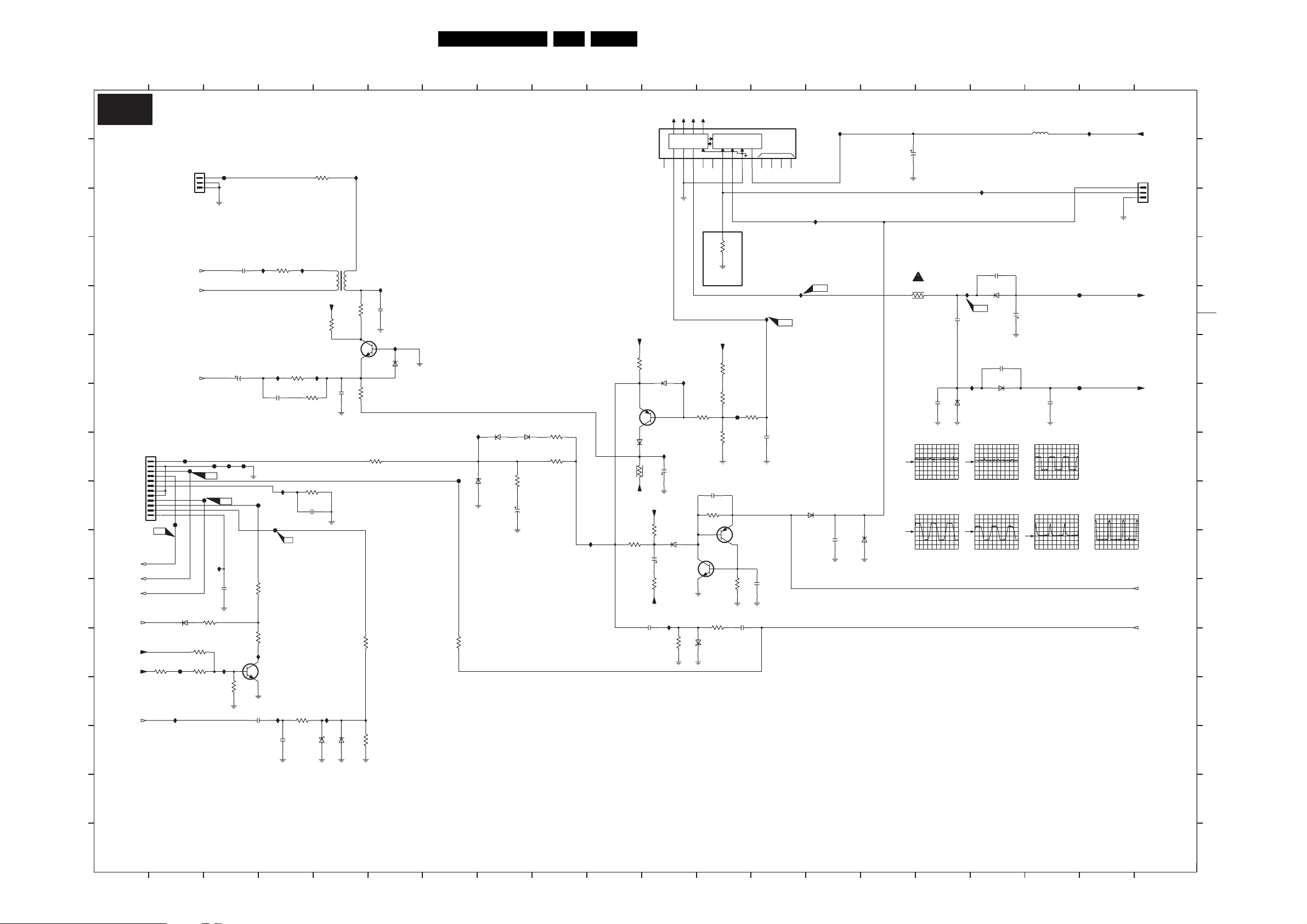
Large Signal Panel
E3
1
2 12
Circuit Diagrams and PWB Layouts
3
4
5
51DPTV465 7.
6
7
8
9
10
11
13 18
14
15
16
17
19
20
A
B
C
D
E
G
K
M
N
F
I
J
L
E3
To SSM
Panel
1510
VPULSE
HOT-COLLECTOR
VERT
VERT
FLASH
VDOA
VDOB
+15V
-200V
EWO
HOUT
HDR2K4 LARGE SIGNAL PANEL (AP)
DYN FOCUS
DYN-FOCUS-LOW
VERT-PARABOLA
F933
.7V
.7V
4.7V
2.9V
.6V
1.1V
4V
F936
6902
BZX79-C18
F946
I958
1504
B3P-LV-TA
1
2
3
1.5V
F935
3926
220K
3935
2M2
F938
2-H19
2-G19
2-I19
3928
10K
I955
1
4
+330V
I914
W8073
8
6
5901
3907
330K
180.5V
BF478
10n
2904
6906
6910
BZX79-C8V2
I917
2n2
1K5
2902
3909
-.37V
3933
3940
I924
6901
BAS216
27K
3936
10R
10R
100K
7901
3905
F900
181V
I918
2901
100n
2903
50V 4u7
F941
F934
F942
F2
L2
I941
1n0
2906
I957
-.4V
18K
3932
3901
100R
I927
2910
33n
I936
F939
F904
L39
1K0
3931
3930
100R
I956
.6V
7902
BC847B
I954
2908
220p
2907
3902
1K5
I919
I928
3904
22K
3900
2K7
3929
10K
100n
2905
3934
4K7
4n7
BAT85
To
Focus/G2
Block
ABL
EHT
HDR
SCO
HFP
DPC
1510
B12B-EH-A
1
2
3
4
5
6
7
8
9
10
11
12
2-J12
2-K12
2-E1
2-O19
2-H19
DYN-FOCUS-HIGH
F3
3927
2M2
F937
3925
BGR
VFOC
EHT EHT
EHT
5904
HVG
GND
NC NC
4
5
DRIVER & CONTROL
ON /
OVP
TEST
OFF GND
VB+
91011
678
2.1V
3903
131V
9.8V
220K
MT
13
14
12
TRANSFORMER
VAUX
ABL RTN VAUX
NC
123
-2.2V
RESERVED
I920
420Vp-p
I923
140Vp-p
+15V
2K2
3915
1.3V
BC327-25
7903
6903
I931
BZX79-C4V7
6905
BZX79-C3V9
1K0
6904
3923
BAS216
3937
2911
470R
3924
47K
4R7
47u
I935
-12.4V
6909
3916
-13V
3920
120K
2926
4n7
1N4148
10R
+15V
3919
10u
1K0
+15V
6908
BAS216
.7V
I932
2912
120K
3906
I929
10u
6912
BAS216
2914
I949
3922
7904
BC847B
10K
+130VS
6K8
3910
56K
3911
1K0
9.8V
BAT254
F945
8K2
3913
2921
100n
3917
22K
10.4V
BC857B
7905
.09V
3918
680R
2927
3921
470K
100n
3914
6919
L38
3912
1K5
100n
2913
2915
100n
6914
BAS216
I910
47u
2917
I915
I916
2922
L36
3908
340Vp-p
22R
2919
2925
100p
6915
F2
1V / div AC
10µs / div
I921
1n0
I925
BYV27-600
F3
100p
6917
BYV27-400
L37
BYV27-600
1V / div AC
10µs / div
2924
100p
6916
L36
100n
2916
6913
BAS216
1V / div AC
2µs / div
1V / div AC (x100)
2µs / div
5902
47u
4u7
2920
2918
L2
2V / div AC
10µs / div
L38L37
50mV / div AC (x100)
5ms / div
I912
(-216V Measured)
F902
F903
(+345V Measured)
2n2
+130VHV
1901
B3B-EH-A
-200V
+330V
1
TEST
2
3
L39
2V / div AC
10µs / div
HVG-ON
2-I19
DM-INPUT
2-H19
A
B
C
D
E
F
G
HH
I
J
K
L
M
N
O
P
3135 033 3425.3
1
O
P
E_15000_027.eps
191004
2
4
5
6
83
9
10
11
12
13
147
15
16
18
19
2017
Page 52
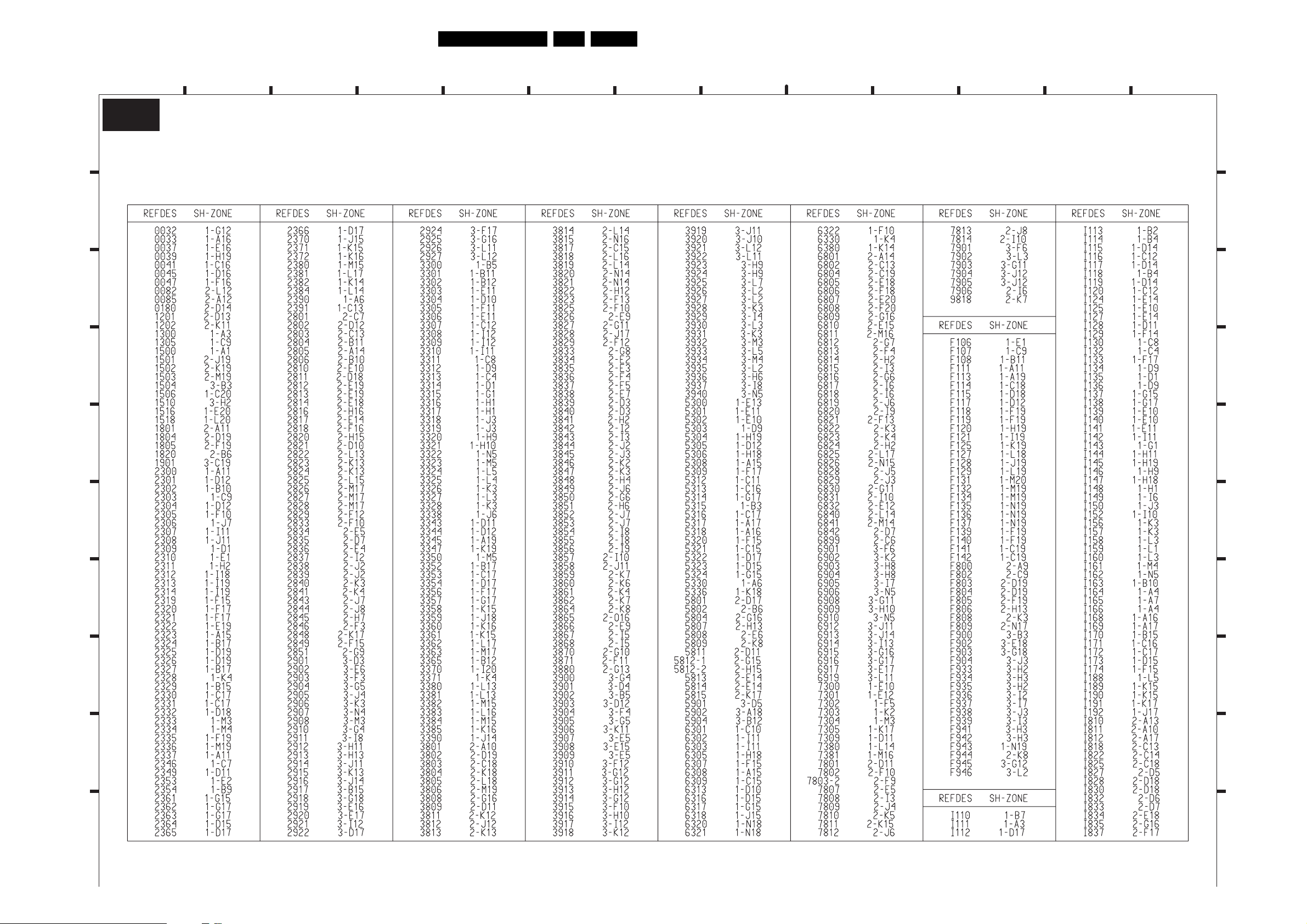
Circuit Diagrams and PWB Layouts
J
H
G
F
E
D
C
B
A
E4
Mapping Large Signal Panel E1-E3 (Part 1)
52DPTV465 7.
54321
6
7
1312111098
E4
KDR2K4 LARGE SIGNAL PANEL (AP)
A
B
C
D
E
G
H
F
I
I
J
3135 033 3425.3
E_15000_028.eps
Page 53
Circuit Diagrams and PWB Layouts
E5
Mapping Large Signal Panel E1-E3 (Part 2)
53DPTV465 7.
A
B
C
D
E5
54321
HDR2K4 LARGE SIGNAL PANEL (AP)
Personal Notes:
A
B
C
D
G
H
E
F
E
F
G
H
II
J
3135 033 3425.3
15432
E_15000_029.eps
191004
J
E_06532_012.eps
131004
Page 54
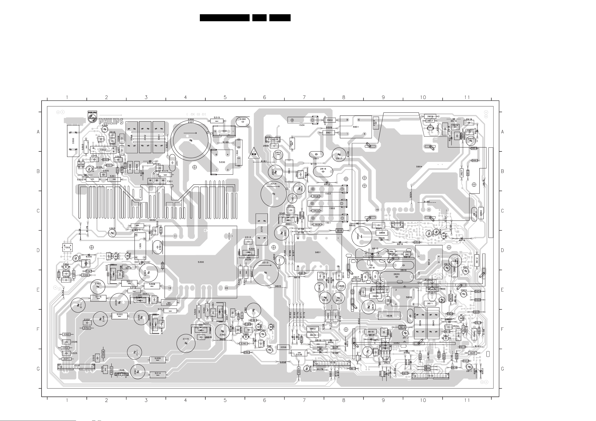
Circuit Diagrams and PWB Layouts
Layout Large Signal Panel (Top Side)
0032 C3
0033 D2
0037 F5
0039 D6
0041 E3
0045 F3
0047 F5
0082 F9
0085 C6
0180 D9
1201 E10
1202 A6
1300 B5
1305 D3
1500 A5
1501 C8
1502 C8
1503 C8
1504 A7
1506 G2
1510 G10
1516 G1
1518 G8
1801 C7
1804 E7
1805 E8
1901 C9
2300 A4
2301 B4
2302 C3
2303 C2
2304 B3
2305 B2
2306 A2
2307 A2
2308 A2
2309 B2
2310 A2
2311 A2
2312 D6
2313 D6
2314 B6
2319 F5
2320 F4
2321 G3
2322 G2
2323 E2
2324 E3
2325 G1
2326 F1
2327 E2
2328 D1
2329 E3
2330 E2
2331 E1
2332 F1
2333 E1
2334 E1
2335 G2
2336 G7
2337 A4
2346 B2
2349 D2
2353 A2
2354 B2
2361 E5
2362 F5
2363 G3
2364 F3
2365 F3
2366 F2
2370 F5
2371 F5
2372 F6
2380 F6
2381 F6
2382 F6
2384 F6
2390 A5
2391 D3
2801 D7
2802 B6
2803 B7
2804 B7
2805 C7
2806 A6
2810 D11
2811 E8
2812 E8
2813 E8
2814 E8
2816 B7
2817 E9
2818 D9
2820 E9
2821 E8
2823 G9
2825 G9
2828 F9
2833 E10
2834 F11
2835 E9
2836 F10
2837 D11
2840 C9
2844 D10
2848 G9
2849 E10
2901 B7
2902 A9
2903 E11
2907 E8
2908 E8
2911 G11
2912 F10
2913 C11
2914 D10
2917 B8
2918 A11
2919 A11
2920 A11
2922 A11
2924 A11
2925 A11
3300 A1
3301 A3
3302 A3
3305 B2
3307 C3
3308 B3
3309 B3
3310 B2
3311 B1
3312 B1
3314 B2
3320 B2
3321 B2
3322 D1
3323 E1
3324 G7
3325 E1
3345 D3
3347 E2
3350 E1
3352 F1
3353 F1
3354 F1
3356 G2
3357 G2
3358 F5
3359 F6
3360 F6
3361 F5
3362 G6
3365 A3
3370 C6
3371 G1
3381 F6
3390 F5
3801 B7
3802 F7
3803 E7
3804 C7
3805 C7
3806 C7
3808 D9
3809 E9
3811 G10
3812 G10
3815 G8
3817 C7
3818 F9
3819 F7
3820 F8
3821 F8
3822 E11
3828 F7
3829 F11
3834 G11
3837 F11
3838 F9
3839 F10
3840 F10
3844 F11
3846 D8
3850 D10
3859 B11
3860 C11
3862 B11
3864 A11
3866 F11
3871 E10
54DPTV465 7.
3880 D11
3900 E11
3901 A8
3902 A8
3904 E11
3905 F11
3907 A10
3908 A11
3909 A10
3910 F11
3911 F11
3912 D11
3913 F11
3914 F11
3915 F11
3916 F9
3925 G11
3926 G10
3927 B11
3931 G10
3933 G10
3934 G8
3935 G11
3936 G11
3937 G11
3940 G9
5300 D4
5301 B2
5302 B1
5303 A1
5304 E5
5305 B3
5306 E5
5308 E3
5309 G3
5312 C3
5313 E3
5314 G3
5315 A5
5316 E2
5317 E3
5318 D3
5320 F4
5321 E4
5322 F2
5323 E3
5324 F4
5330 B5
5336 G7
5801 D7
5802 D6
5804 D8
5807 D11
5808 E10
5809 A7
5811 E9
5812 D10
5813 D10
5814 D9
5815 F7
5901 A8
5902 B6
5904 B10
6301 D3
6302 B3
6303 B3
6305 D6
6307 F5
6308 D2
6309 E3
6313 D3
6316 F3
6317 F5
6318 F5
6320 G7
6321 F7
6322 B1
6330 D2
6380 F6
6801 C7
6802 B7
6804 F8
6805 E8
6806 E8
6809 D9
6810 D9
6811 F9
6812 B8
6816 D9
6819 D11
6822 C8
6825 F8
6826 G10
6840 F7
6841 F7
6902 G10
6903 G11
6905 G11
6906 G9
6909 F11
6910 G9
6915 A11
6916 A11
6917 A11
7300 D3
7301 B4
7302 A2
7303 D1
7304 D1
7305 F6
7309 D2
7380 F6
7381 F6
7801 E9
7802 E10
7807 F11
7811 F9
7812 D11
7901 A10
7903 F11
9106 B8
9109 B2
9110 B7
9138 D1
9139 C2
9140 D3
9141 F11
9142 E1
9146 D7
9149 A5
9153 G8
9156 D7
9158 C7
9162 F7
9165 F7
9166 D7
9167 D7
9168 F7
9169 F8
9170 F7
9171 F7
9172 F7
9173 F8
9176 F8
9177 E10
9179 G7
9180 G9
9181 B6
9187 G8
9188 G8
9189 C11
9190 C10
9191 C11
9193 G10
9195 G11
9198 F11
9201 F8
9202 E6
9203 F11
9204 A10
9302 F8
9303 A4
9304 C10
9307 G8
9308 G6
9309 A8
9805 E6
9807 F9
9808 G10
9809 F5
9811 G9
9814 F9
9816 E7
9818 B11
9819 E11
3135 033 3425.3
E_15000_030.eps
061004
Page 55
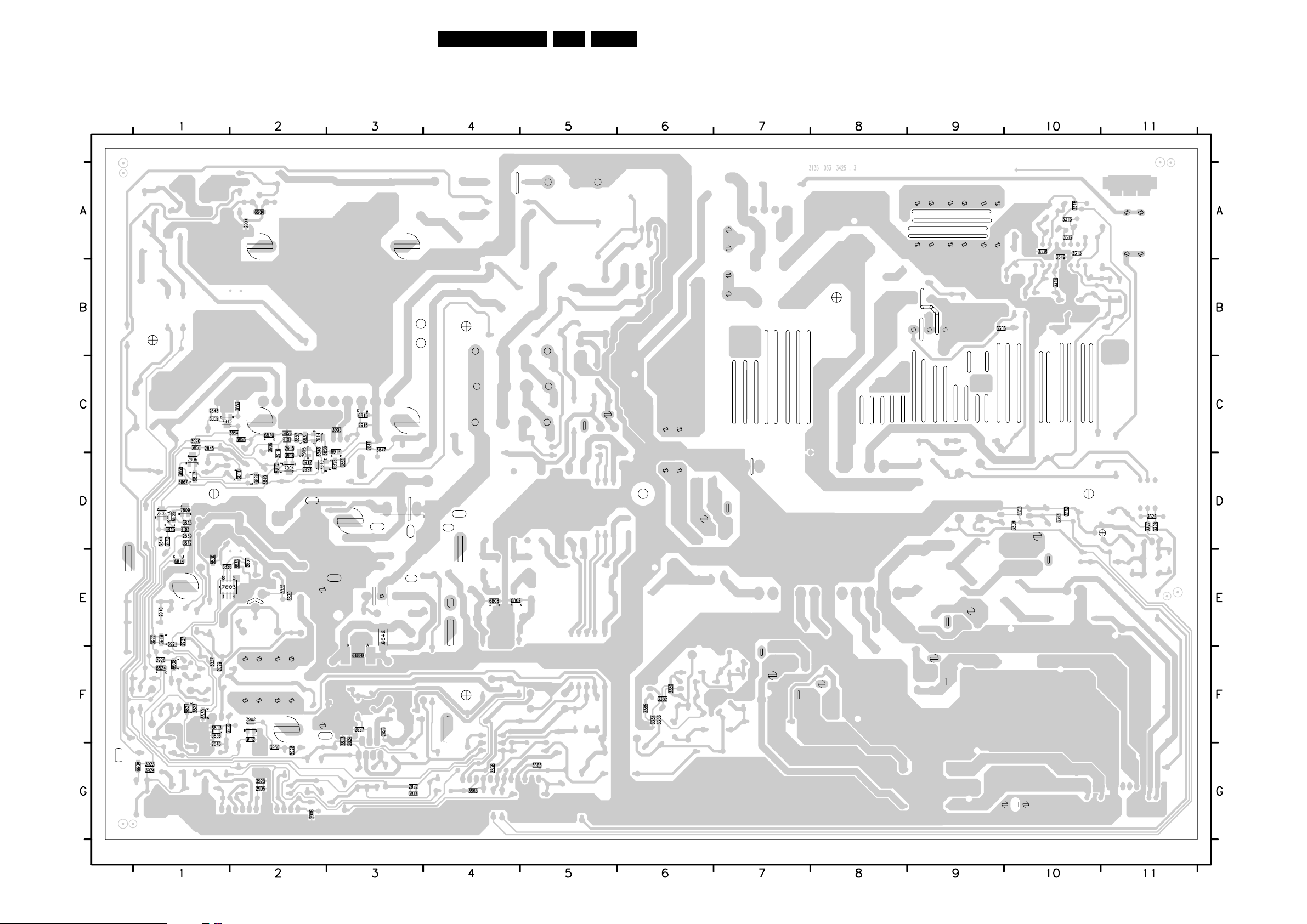
Circuit Diagrams and PWB Layouts
Layout Large Signal Panel (Bottom Side)
2822 G3
2824 F3
2826 F3
2827 F3
2829 F1
2838 G4
2839 D1
2841 C3
2843 C1
2845 C1
2846 G1
2851 E2
2904 A2
2905 G2
2906 G2
2910 E1
2915 C2
2916 C3
2921 D2
2926 F1
2927 E1
3303 D10
3304 D10
3306 B9
3313 A10
3315 A10
3316 A10
3317 A10
3318 B10
3319 A10
3326 D11
3327 D11
3328 D11
3338 A10
3343 D10
3344 D10
3363 G5
3380 F6
3382 F6
3383 F6
3384 F6
3385 F6
3813 F3
3814 G3
3823 F1
3825 E2
3826 E1
3827 F1
3833 E2
3835 F1
3836 F1
3841 D1
3842 D1
3843 D1
3845 D1
3847 C3
55DPTV465 7.
3848 C2
3849 D2
3851 C1
3852 C1
3853 C2
3854 C2
3855 C2
3856 C2
3857 C2
3858 C2
3861 D3
3865 G4
3867 D1
3868 D1
3870 E2
3903 C3
3906 C2
3917 D2
3918 D2
3919 D2
3920 C1
3921 E1
3922 E1
3923 G1
3924 G1
3928 G2
3929 G2
3930 G2
3932 F2
4101 C2
4103 D1
6807 E4
6808 E4
6813 F1
6814 E1
6815 D1
6817 D1
6818 D2
6820 C2
6821 F1
6823 D3
6824 F1
6828 D2
6829 D1
6830 F1
6831 C2
6832 E1
6842 E3
6899 F3
6901 A2
6904 G1
6908 F1
6912 D2
6913 C3
6914 C3
6919 E1
7803 E1
7808 D1
7809 D1
7810 D2
7813 C1
7814 C2
7902 F2
7904 D2
7905 C2
7906 D1
3135 033 3425.3
E_15000_031.eps
111004
Page 56
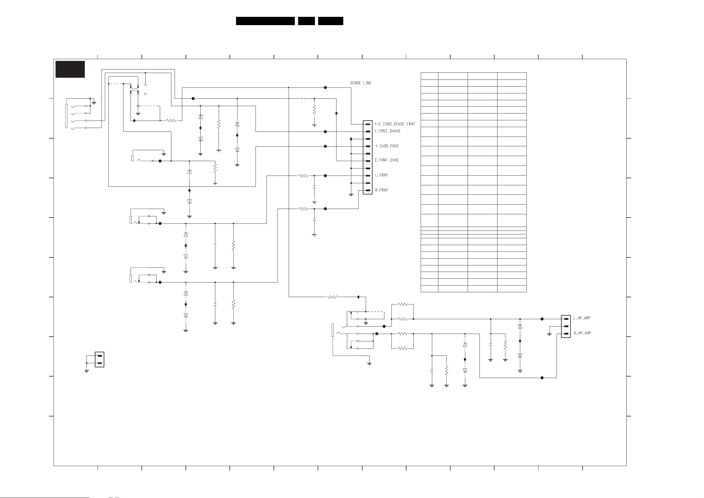
Side Jack Panel
G1
Circuit Diagrams and PWB Layouts
56DPTV465 7.
A
B
C
D
E
F
G
H
1 1312111098
2
3
654
7
A10PTV SIDE JACK PANEL
G1
10
9
11
5
4
6
4001
I000
1001-A
Y_CVBS_FRNT
1001-B
1001-C
1002-B
YKF51-5347
1
2
F010
4
6
5
F011
7
9
8
F012
3030
1K8
L_FRNT
R_FRNT
I004
I015
I003
6006
6007
6008
6009
F014
I002
6003
6005
BZX284-C6V8
BZX284-C6V8
BZX284-C6V8
BZX284-C6V8
C_FRNT_SVHS
Y_FRNT_SVHS
6000
3000
BZX284-C6V8
6002
BZX284-C6V8
3002
BZX284-C6V8
2002
2006
BZX284-C6V8
75R
330p
330p
75R
I023
6001
6004
3006
3009
BZX284-C6V8
BZX284-C6V8
22K
22K
2000
220N
3005
1K0
3007
1K0
3001
2001
2005
F015
75R
F016
F017
F018
330p
F019
330p
3029
3K9
1007
YKB21
I008
I009
I016
1002-A
YKF51-5347
4000
1
2
7
3
8
YKC21-5617
YKC21-5617
YKC21-5617
1337
PCB-TAB4.8x0.5
1
2
Ref Des
1002-A 242202604926
1002-B 242202604926
1007 242202604747
1344 241202000725
2000 223891019854
1335
EH-B
1
2
3
4
5
6
7
8
9
10
3023
F021
10R
3028
10R
3019
10R
3020
10R
5
4002
4
2
3
7
8
1
F020
2008 NOT USED NOT USED 319801706820
2009 NOT USED NOT USED 319801706820
3000 319802157590
3001 319802157590
3019 319802151090
3020 319802151090
3023 319802151090
3026
3027 NOT USED NOT USED 319802151030
3028 319802151090
3029 319802153920
3030
4000
4001 NOT USED 319802190020 NOT USED
4002
6000 934038640115
6001 934038640115
6002
6004
6010 934038640115
6011 934038640115
6012
6013 934038640115
3135_037_10581
FN1
YKF51-5347
YKF51-5347
YKB21
EH-B
220N
75R
75R
10R
10R
10R
NOT USED NOT USED 319802151030
10R
3K9
319802151820
1K8
NOT USED 319802190020 NOT USED
NOT USED 319802190020 NOT USED
BZX284-C6V8
BZX284-C6V8
934038640115
BZX284-C6V8
934038640115
BZX284-C6V8
BZX284-C6V8
BZX284-C6V8
934038640115
BZX284-C6V8
BZX284-C6V8
10K
6n8
3026
2008
3135_037_12321
FN0
NOT USED NOT USED
NOT USED
NOT USED NOT USED
NOT USED NOT USED
NOT USED
NOT USED NOT USED
NOT USED NOT USED
NOT USED
NOT USED NOT USED
NOT USED NOT USED
NOT USED
319802153920
3K9
319802151820
1K8
NOT USED NOT USED
NOT USED NOT USED
NOT USED NOT USED
NOT USED NOT USED
NOT USED NOT USED
NOT USED NOT USED
NOT USED NOT USED
NOT USED NOT USED
6011
BZX284-C6V8
I021
6010
BZX284-C6V8
2009
RESERVED
FN5
NOT USED
NOT USED
6n8
6n8
NOT USED
10K
10K
NOT USED
NOT USED
NOT USED
6n8
3027
10K
I022
6012
6013
F023
BZX284-C6V8
BZX284-C6V8
F022
1
2
3
EH-B
1344
A
B
C
D
E
F
G
H
I
NOTES
1. CAPACITANCE VALUES ARE IN FARADS:
m=MILI u=MICRO n=NANO p=PICO f=FEMTO
2. RESISTANCE VALUES ARE IN OHMS:
J
R=OHM K=KILO M=MEGA G=GIGA T=TERA
3. SAFETY TRIANGE REPRESENTS PCEC REPLACEMENT PART ONLY.
4. FOR VALUE SEE TABLE.
*
3135 033 3217.4
1
I
J
E_15000_032.eps
191004
5432
6891011
7
12 13
Page 57
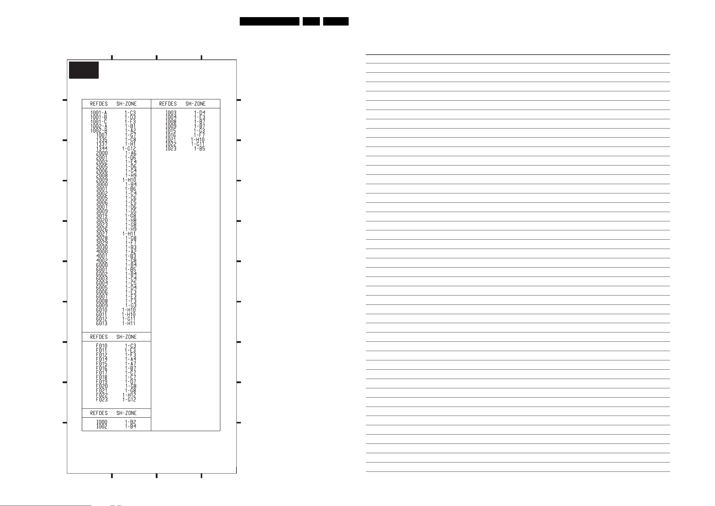
Circuit Diagrams and PWB Layouts
G2
Mapping Side Jack Panel G1
57DPTV465 7.
A
B
321
Personal Notes:
A10PTV SIDE JACK PANEL
G2
A
B
C
D
E
E
F
F
G
H
I
I
J
3135 033 3217.4
132
E_15000_033.eps
191004
J
E_06532_012.eps
131004
Page 58
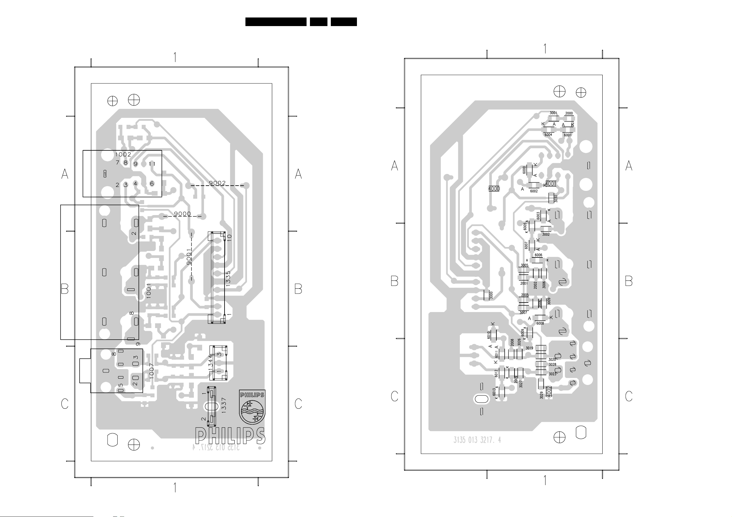
Circuit Diagrams and PWB Layouts
58DPTV465 7.
Layout Side Jack Panel (Top Side)
1001 B1
1002 A1
1007 C1
1335 B1
1337 C1
1344 C1
9000 A1
9001 B1
9002 A1
Layout Side Jack Panel (Bottom Side)
2000 A1
2001 B1
2002 B1
2005 B1
2006 B1
2008 C1
2009 C1
3000 B1
3001 A1
3002 B1
3005 B1
3006 B1
3007 B1
3009 B1
3019 C1
3020 C1
3023 C1
3026 C1
3027 C1
3028 C1
3029 C1
3030 A1
4000 A1
4001 A1
4002 C1
6000 A1
6001 A1
6002 A1
6003 A1
6004 A1
6005 B1
6006 B1
6007 B1
6008 B1
6009 B1
6010 B1
6011 C1
6012 C1
6013 C1
3135 033 3217.4
E_15000_034.eps
111004
3135 033 3217.4
E_15000_035.eps
111004
Page 59
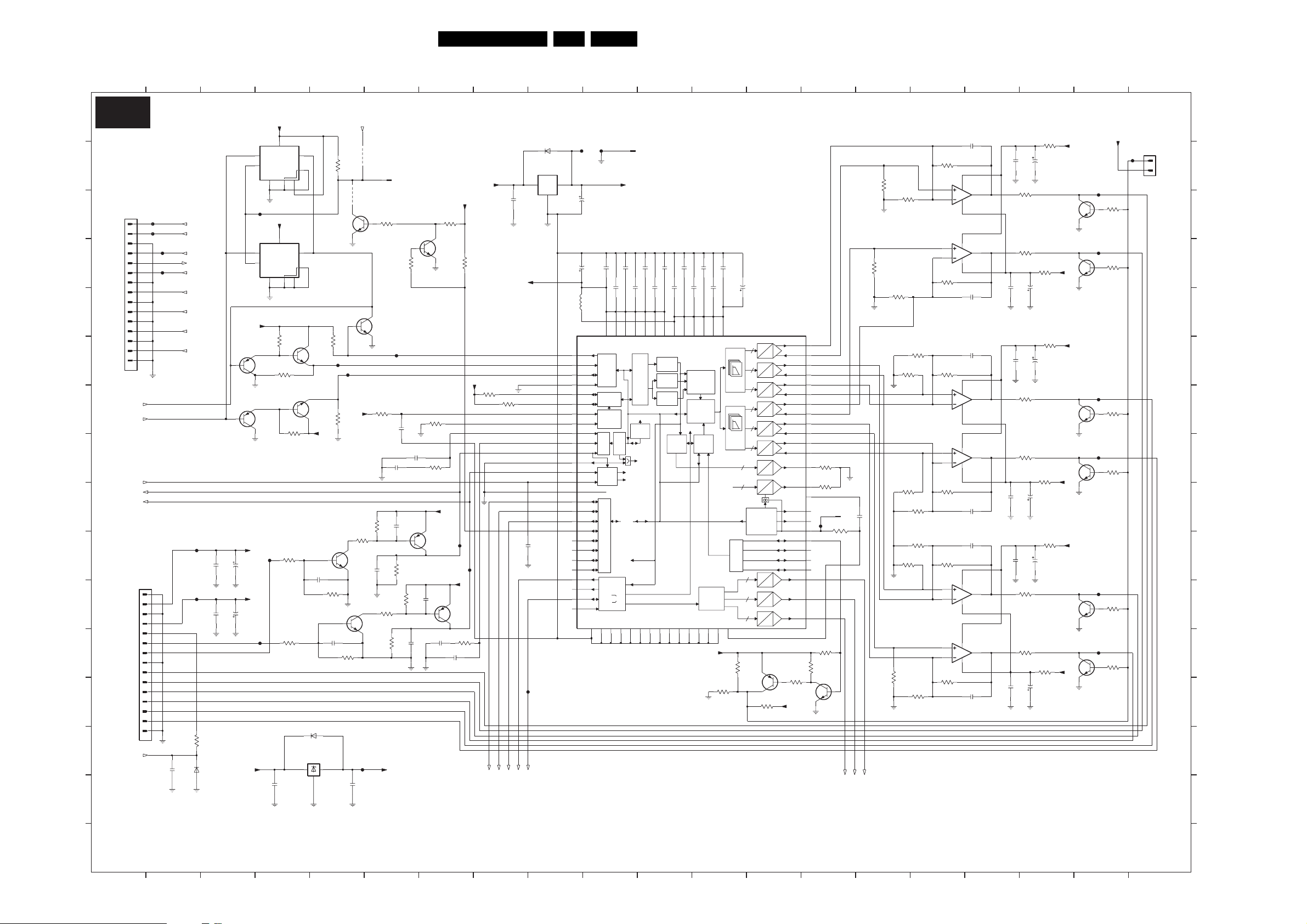
ACS Module
H1
1
23 8
Circuit Diagrams and PWB Layouts
4
5
67
59DPTV465 7.
10 11
12
14
1615 1918
17
20139
A
H1
B
Connector to SSM Panel
C
D
E
F
G
1000
SDA_B
SCL_B
JL
1617
1
2
3
4
5
6
7
8
9
10
11
12
13
14
15
3-K2,2-M3
3-L2,2-J3
H
Reset_ST
SYNC_H
SYNC_V
I
3-L8,2-K15
J
Connector to SSM Panel
K
L
M
N
ON_OFF
2-K15
O
P
3135 013 3233.3
1
ACS Module
3-D2
2-L15
1001
F101
F102
JL
1
2
3
4
5
6
7
8
9
10
11
12
13
14
15
1617
F104
F106
3-H5
3-I5
3-M2,2-H15
2-L3
3-M2,2-H15
3-D16
3-F16
3-G16
3-I16
VBLNK
HBLNK
2005
RV
RH
GV
GH
BV
BH
100p
SCL_A_Txd
SDA_A_Rxd
SCL_C
HORIZ_SYNC
SDA_C
R
G
B
BLANK
F112
F114
3005
100R
6006
BAS216
2004
2006
+5V
7000
8
M24128
VCC
6
SCL
7
WC_
VSS
F700
NOT USED
7001
M24128
SCL6SDA
7
WC_
VSS
+3.3V
BC857B
7021
BC857B
7024
+9V
F117
10u
2001
100n
-8V
10u
2003
100n
F116
+9V
5
SDA
3
5
3
7020
BC847B
BC847B
7023
6001
BAS216
7007
L78M05
1IN3
10K
10K
F708
+3.3V
2021
120p
3025
1K5
2024
120p
OUT
2
GND
5
NC
4
12
+5V
8
VCC
NC
12
4
10K
3011
10K
3012
3013
4K7
3024
5K6
3029
5K6
1u0
2007
4
2-L3
NVM_wc_N
6000
100n
TBU2
2010
+3.3V
2-C3
BLANK_ST
2002
3-I13
OPTT
BAS216
7006
LD1117DT33C
3
COM
10n
F774
3-L8,2-K3
4000
3079
3010
F709
4K7
3014
7026
BC847B
3030
1K5
2008
+3.3V
3026
4001
2K2
F001
100n
BC847B
7027
BC847B
WRITE PROTECT
7036
7022
BC847B
3020
82K
2K2
120p
1002
1
3080
1K0
1K0
F707
33p
2016
2019
2020
1n5
10n
2022
120p
3027
4K7
2023
3028
1K5
3032
3031
2K2
4K7
120p
3033
+5V
3081
1K0
7037
BC847B
3083
3021
10K
3023
15K
+3.3V
BC857B
7025
F727
SYNC_H
2025
120p
BC857B
2017
2026
10n
2018
1n5
76109
F728
+3.3V
7028
SYNC_V
+3.3V
1K0
3022
+5V
3082
+3.3V
3016
3015
10K
10K
15K
2-C3
2-C3
TBU1
TBU0
832 12
F002
2
OUTIN
1
2011
2040
7
10u
10u
5006
SDAO
SDAI8
SCLS9
ADS071
SDAM1
SCLM2
OSCL21
GRES22
FLT225
FILT24
SYNH27
ECLK14
SYNV28
REST13
TEST11
TBU040
TBU139
TBU238
TBU337
TBU436
TBU535
TBU634
TBU733
VBLK10
MLIN75
OPTT74
OPTI72
GNDA47GNDB59GNDC
F003
2014
5
VCCQ
2
I C
SLAVE
2
I C
MASTER
400 KHz
2
I C
OSC.
PLL
VERT.
FILTER
BUS EXPANDER
TIMEBASE
DAC
GRID
1003
GND
+3.3V
100n
2034
100n
2029
2009
100n
73
12
VCCL
VCCN
VCCM
MEM
CTRL
DAC ENABLE
START
LOGIC
PLL
LOGIC
SYSTEM
RESET
VSYNC
BUS
2
I C
PARALLEL
BUS
MEMORY
REGISTER
TIMING
GNDD20GNDF23GNDG43GNDH
67
1
2035
100n
2028
100n
2032
100n
VCCC
LOOP
70
2033
62
011111h
100n
VCCA50VCCB
100n
VERT
FILTER
HOR.
FILTER
10u
2041
7002
STV2050A
D
14
A
D
14
A
D
14
A
D
14
A
D
14
A
D
14
A
D
6
A
D
6
A
IREF
100n
2030
100n
2013
2031
2015
31
VCCJ
GREEN
100n
VCCH
RED
MEM
MEM
BLUE
MEM
42
VCCG
FOCUS
PROC.
44
FOCUS
100n
26
VCCF
POLATION
2012
19
VCCD
INTER-
GAIN/
OFFSET
100n
6
32
VCCK
SYS
CLK
BANDGAP
PORT
INTERF.
D
4
A
VIDEO
PATTERN
GEN.
GNDJ29GNDK4GNDL30GNDM76GNDN15GNDP56GNDQ
41 53
NOTES
1. CAPACITANCE VALUES ARE IN FARADS:
m=MILI u=MICRO n=NANO p=PICO f=FEMTO
2. RESISTANCE VALUES ARE IN OHMS:
R=OHM K=KILO M=MEGA G=GIGA T=TERA
3. SAFETY TRIANGE REPRESENTS PCEC REPLACEMENT PART ONLY.
4. FOR VALUE SEE TABLE.
*
GNDI
3
+5V
3044
10K
D
4
A
D
4
A
5K6
3043
BC857B
7038
3045
10K
NOT USED
11
DNGV 63
DNRH 51
DAGH 49
DNGH 48
OGAV
OGAH 57
PORC 78
3042
-8V
DARV
DNRV 65
DAGV 64
DABV 61
DNBV 60
DARH 52
DABH 46
DNBH 45
FOCS 69
FOCR 68
REFC 55
REFN 54
POUT 77
PORA 80
PORB 79
VIDR 16
VIDG 17
VIDB 18
5K6
BC847B
66
3035
10K
3036
10K
BAND GAP ADJUST
58
F754
4K7
3040
33K
3041
7029
1413
3049
100R
3048
100R
3064
100R
3063
100R
3058
100R
3059
100R
3074
100R
1005
1
2027
120p
3034
1K
3-E13
3-D13
3-G13
RED_ST
GRN_ST
BLUE_ST
3073
100R
3068
100R
100R
3054
100R
3053
100R
2042
10p
3050
10K
7004-2
LM833D
8
5
7
6
4
7004-1
8
LM833D
3
1
2
4
3065
10K
2045
10p
2044
10p
3060
10K
7003-2
LM833D
8
5
7
6
4
7003-1
LM833D
8
3
1
2
4
3075
10K
2047
10p
2046
10p
30703069
10K
7005-2
LM833D
8
5
7
6
4
7005-1
LM833D
8
3
1
2
4
3055
10K
2043
10p
2054
2052
2050
2048
2058
2056
3087
+9V
100R
10u
2055
100n
3051
330R
3066
330R
2053
100n
100n
2051
3061
330R
3076
330R
2049
100n
2059
100n
3071
330R
3056
330R
100n
2057
RV
7032
BC847B
RH
3086
-8V
100R
10u
3085
+9V
100R
10u
BV
7030
BC847B
BH
3084
-8V
100R
10u
3089
+9V
100R
10u
GV
7034
BC847B
GH
3088
-8V
100R
10u
181716 2015
F005
F006
BC847B
F007
F008
BC847B
F009
F010
BC847B
7033
7031
7035
19
+5V
3052
220R
3067
220R
3062
220R
3077
220R
3072
220R
3057
220R
1004
F004
1
2
EH-B
E_15000_036.eps
A
B
C
D
E
F
G
H
I
J
K
L
M
N
O
P
191004
Page 60
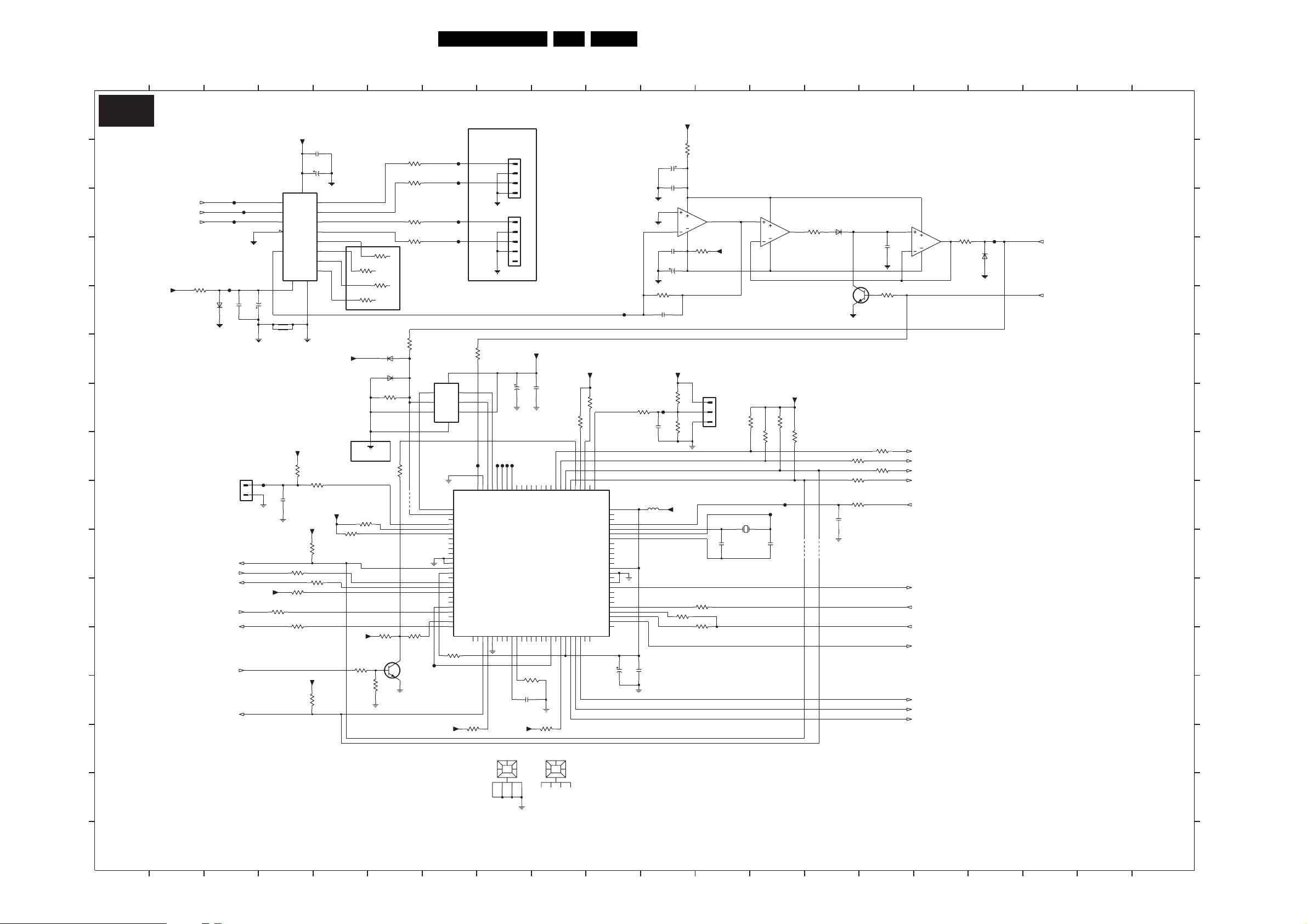
Circuit Diagrams and PWB Layouts
H2
ACS Module
1234
5678
60DPTV465 7.
910
11 12
13
14
15 16
17
18
19
20
A
B
C
D
E
G
H
K
M
N
O
F
I
J
L
H2
ACS Module
SENSOR MUX
TBU0
TBU1
TBU2
-8V
3405
150R
F019
1-N8
1-N8
F021
1-N8
F022
6405
2201
BZX284-C5V1
KEYBOARD
SCL_B
3-L2,1-G2
Rxd
Txd
3-H2
OPTT
3-L8,1-N8
NVM_wc_N
1-A5
HORIZ_SYNC
SDA_B
3-K2,1-G2
F020
ADC_GND
2252
100n
1019
1
2
EH-B
3-J5
1-D2
F014
+3.3V
7141
74HCT4051D
100u
3233
100R
+5V
+5V
2200
100n
2251
16V
100u
16
VCC
11
S0
10
S1
9
S2
6
E_
3
Z
13
Y0
14
Y1
15
Y2
12
Y3
1
Y4
5
Y5
2
Y6
4
Y7
VEE
GND
7
8
100R
100R
3298
100R
3299
3400
100R
3401
ADC_GND
+3.3V
+3.3V
2K2
3224
3223
4K7
10n
2224
+5V
3K3
3211
3212
100R
3214
3216
100R
1K0
3215
100R
+5V
3K3
3210
+3.3V
3221
1K0
+3.3V
ADC_GND
3220
1K0
3226
22K
3227
7227
BF570
NOT USED
6208
BAS216
6209
BAS216
3242
100R
NOT USED
3225
1K0
10K
3294
SENSOR_1
100R
3295
SENSOR_2
100R
3296
SENSOR_3
100R
3297
SENSOR_4
100R
1K0
3243
7101
TLV0831CD
VCC
1
2
IN+
IN-3REF
GND
3232
100R
4306
3231
100R
F142
+3.3V
F015
F016
F017
F018
8
CLK7CS_
DO
4
1
2
3
4
5
6
7
8
9
10
11
12
13
14
15
16
17
18
19
20
21
22
23
24
25
3213
1K0
6
5
F100
7100
SAA5667HL
P2.7|PWM6
P3.0|ADC0
A17-LN
P3.1|ADC1
P3.2|ADC2
P3.3|ADC3
A15-LN
A14
RD_
WR_
VSSC1
VSSP1
P0.5
EA_
A7
P0.0|TX
P0.1|RX
P0.2|INT2
PSEN_
ALE
VPE1
P0.3|INT3
A6
P0.4|INT4
P3.7
3217
1K0
INPUT FROM
SENSOR
ADC_GND
ADC_GND
SH_CLEAR
1K0
3241
F196
100
96
97
98
99
VSSC3
P2.4|PWM3
P2.5|PWM4
P2.6|PWM5
P2.0|TPWM
VSSA
P0.628P0.7|T2
CVBS031CVBS1
A427A5
30
29
26
TOP
SHEILD
1234
1010
1
2
3
4
EH-B
1011
1
2
3
4
5
EH-B
2211
F194
F195
94
95
P2.1|PWM0
P2.2|PWM1
P2.3|PWM2
SYNC-FILTER
A15-BK
32
33
+3.3V
0001
F193
93
34
IREF
92
35
+3.3V
10u
90
AD691AD7
A1237A13
36
3240
24K
2223
100n
2210
100n
AD186AD287AD388AD489AD5
FRAME41G
A239A3
A1
38
40
3222
1K0
0002
HEATSINK
1234
+3.3V +5V
1K0
3218
1K0
3219
76
78
79
80
83
84
81
82
P1.3|T1
P1.2|INT0
P1.4|SCL1
P1.6|SCL0
P1.7|SDA0
R
VDDA
P3.4|PWM7|T2EX
B46CORB
48
45
44
47
BOTTOM
SHEILD
A16-LN
P1.1|T0
XTALOUT
OSCGND
ROMBK0
ROMBK1
ROMBK2
RAMBK1
A0
49
77
P1.0|INT1
VDDP
MVX-RD
RESET
RESET_
XTALIN
MVX-WR
VDDC
VSSC2
INTD_
VSSP2
P3.6
VSYNC
P3.5
HSYNC
VDS
RAMBK0
50
A8
A9
A10
A11
AD0
VPE2
85
P1.5|SDA1
42
43
3418
100R
2279
10u
2280
100n
7140-A
3
4
ADC_GND
3291
33K
F012
75
74
73
72
71
70
69
68
67
66
65
64
63
62
61
60
59
58
57
56
55
54
53
52
51
2207
2250
3n3
F013
3235
100R
2235
5200
100u
47u
2206
100n
TL074
2
2281
100n
2282
16V
10u
3236
10n
3237
1
11
3419
-8V
100R
IR
1018
1
6K8
2
3
10K
EH-B
+3.3V
1200
DSX840
12M
56p
2204
3228
100R
3230
100R
3229
100R
5
4
6
11
4K7
3206
4K7
3207
2205
SAMPLE & HOLD
7140-B
TL074
3292
7
100R
ADC_GND
+5V
3K3
3208
NOT USED
3K3
3209
NOT USED
F172
F170
56p
4308
4307
6230
BAS216
BC847B
2311
7140-C
10
4
TL074
9
2253
470n
ADC_GND
3204
100R
3202
100R
3234
100R
3205
100R
3203
100R
3293
1K0
3-M2,1-D2
3-M2,1-D2
3-I2
3-H2
3-E2
1-N2
3-L8,1-I2
1-I2
3-H15
3-C15
3-E15
3-F15
7540
10n
8
11
SDA_C
SCL_C
SDA_A
SCL_A
Reset_N
ON_OFF
SYNC_V
SYNC_H
BLANK_uP
RED_uP
GRN_uP
BLUE_uP
3282
100R
6231
ADC_GND
F011
BZX284-C5V1
3-M8
ADC_IN
3-L8
SH_CLEAR
A
B
C
D
E
F
G
H
I
J
K
L
M
N
O
P
3135 013 3233.3
1 20
AUTO CONVERGENCE
3135 013 32333 01
32
5
6
7
89
12114
141310
171615
18
19
E_15000_037.eps
P
191004
Page 61
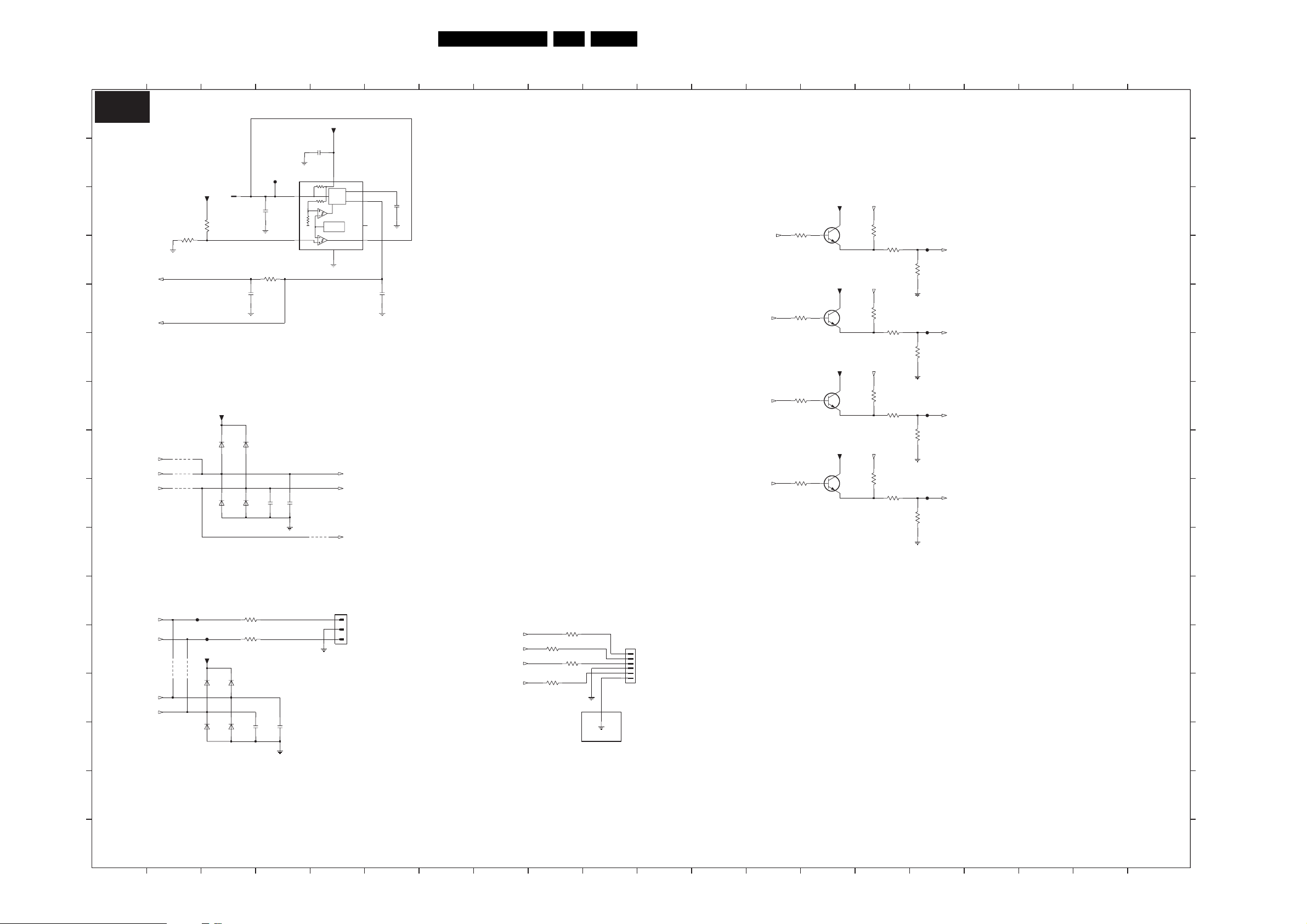
ACS Module
H3
12
Circuit Diagrams and PWB Layouts
3456
61DPTV465 7.
7
8
9
10 11 12 13 14
15
16 17
18
19
20
A
B
C
D
E
F
G
H
J
I
H3
ACS Module
+3.3V
2312
100n
3331
100R
2317
7301
TPS3707-33D
100n
10p
10p
2318
2
14K
VDD
RESET 8
RESET
MR_1
LOGIC&
RESET_ 7
TIMER
REF VOLT
OF 1.25V
PFI4 PFO_ 5
GND
3
RESET
1-C2
SDA_A_Rxd
1-C2
4304
Rxd
2-J3
RESET TESTPOINT
F301
1302
2313
10n
2310
Reset_ST
Reset_N
2-I15
RESET
+9V
1
RT-01T-1.0B
10K
3332
3333
2K2
1-I2
IIC BUS
+5V
6308
6309
BAS216
BAS216
BAS216
6311
BAS216
4302
Txd
2-K3
2-I15
2-H15
4303
NOT USED
4305
NOT USED
6310
SCL_A SCL_A_Txd
SDA_A
A
B
OSD "OR" CIRCUIT
100n
2314
6
NC
2315
100n
RED_ST
GRN_ST
BLUE_ST
BLANK_ST
1-N14
1-N14
1-N8
1-N15
3329
1K0
3328
1K0
3327
1K0
3326
1K0
+5V
+5V
+5V
+5V
7014
BC847B
7015
BC847B
7016
BC847B
7017
BC847B
3306
2-M15 2-M15
3307
2-M15
3308
2-L15
3309
RED_uP
100R
3314
47R
GRN_uP
100R
3315
47R
BLUE_uP
100R
3316
47R
BLANK_uP
100R
3317
47R
C
F023
R
1-E2
3322
100R
NOT USED
D
E
F024
G
1-E2
3323
100R
NOT USED
F025
B
1-E2
3324
100R
F
G
H
F026
BLANK
1-F2
3325
100R
NOT USED NOT USED
I
J
K
SDA_B
SCL_B
L
M
SDA_C
SCL_C
N
O
P
3135 013 3233.3
2-M3,1-G2
2-J3,1-G2
2-H15,1-D2
2-H15,1-D2
I2C BUS B
TEST CONNECT
1300
F027
F028
+5V
4300
4301
NOT USED
NOT USED
6312
BAS216
3201
100R
3200
100R
6313
BAS216
JQ-S
1
SDA_B
2
GND
3
SCL_B
SYNC_V
OPTT
SH_CLEAR
ADC_IN
2-K15,1-I2
2-K3,1-N8
2-E18
2-D18
3349
100R
3351
100R
100R
100R
3348
1301
1
B6B-EH-A
2
COMPUTER
3
DEVELOPMENT
4
CONNECTOR
5
6
3350
K
L
M
6314
BAS216
BAS216
ADC_GND
10p
10p
2320
2319
6315
N
O
AUTO CONVERGENCE
E_15000_038.eps
2
31
5
6
7
8121110
9
13
14
1615
1817
20194
P
191004
Page 62
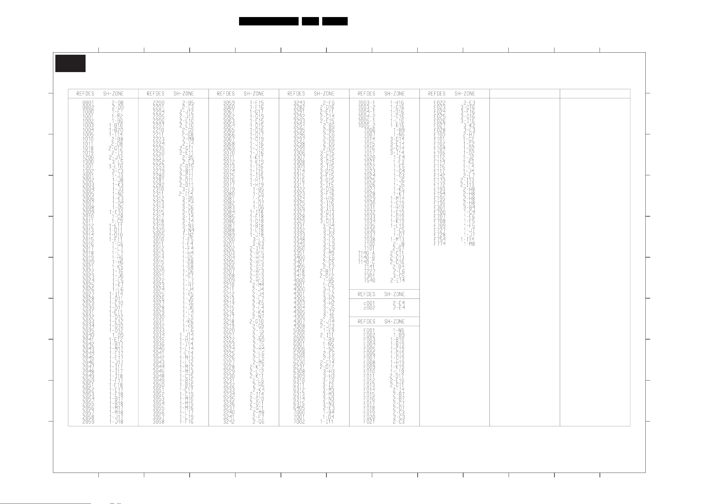
Circuit Diagrams and PWB Layouts
H4
Mapping ACS Module H1-H3
62DPTV465 7.
A
B
C
D
H4
AUTO CONVERGENCE
654321
7
1312111098
A
B
C
D
E
F
G
H
E
F
G
H
I
I
J
3135 013 3233.3
1
AUTO CONVERGENCE
65432
7
J
E_15000_039.eps
111004
1211109138
Page 63
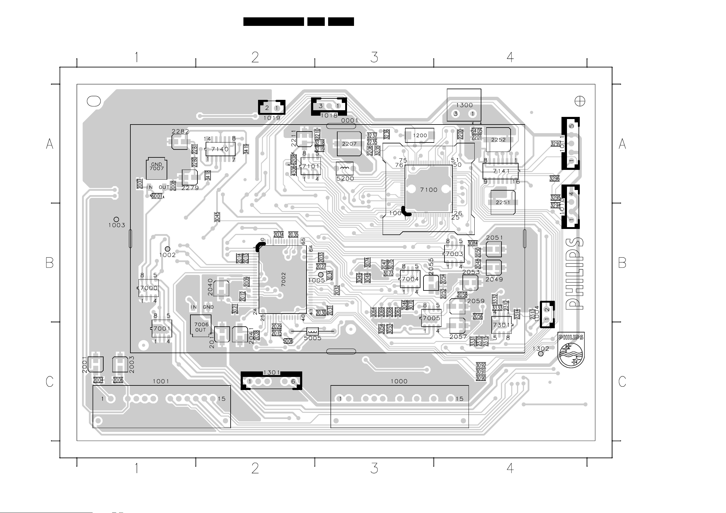
Circuit Diagrams and PWB Layouts
Layout ACS Panel (Top Side)
63DPTV465 7.
3135 013 3233.3
E_15000_040.eps
111004
0001 A3
1000 C3
1001 C1
1002 B1
1003 B1
1004 B4
1005 B3
1010 B4
1011 A4
1018 A3
1019 A2
1200 A3
1300 A4
1301 C2
1302 C4
2001 C1
2003 C1
2004 C1
2006 C1
2007 A1
2008 A1
2009 B2
2011 C2
2012 B2
2013 B2
2014 B2
2015 C2
2027 B3
2028 C2
2029 C2
2030 B3
2031 B3
2032 B3
2033 B3
2034 B2
2035 B2
2040 B2
2041 C2
2046 B3
2047 B3
2048 B4
2049 B4
2050 B4
2051 B4
2052 B4
2053 B4
2054 B4
2055 B3
2056 B4
2057 C4
2058 B4
2059 B4
2200 A4
2201 A4
2206 A3
2207 A3
2210 A3
2211 A2
2235 A3
2251 A4
2252 A4
2279 A1
2280 A1
2281 A1
2282 A1
2310 C4
2312 B4
2313 B4
2314 B4
2315 C4
3021 B2
3034 B3
3045 B2
3048 B3
3049 B3
3053 C3
3054 C3
3063 B3
3064 B3
3068 B3
3069 B3
3070 B3
3073 B3
3074 B3
3075 B3
3084 B4
3090 C4
3091 C4
3092 C4
3218 A3
3219 A3
3235 A3
3236 A3
3237 A3
3294 B4
3295 A4
3296 A4
3297 A4
3331 C4
3332 B4
3333 B4
3418 A2
3419 A2
4306 A2
5005 C2
5006 C2
5200 A3
6001 A1
6208 A2
6405 A4
7000 B1
7001 C1
7002 B2
7003 B4
7004 B3
7005 B3
7006 C2
7007 A1
7100 A3
7101 A2
7140 A2
7141 A4
7301 C4
Page 64
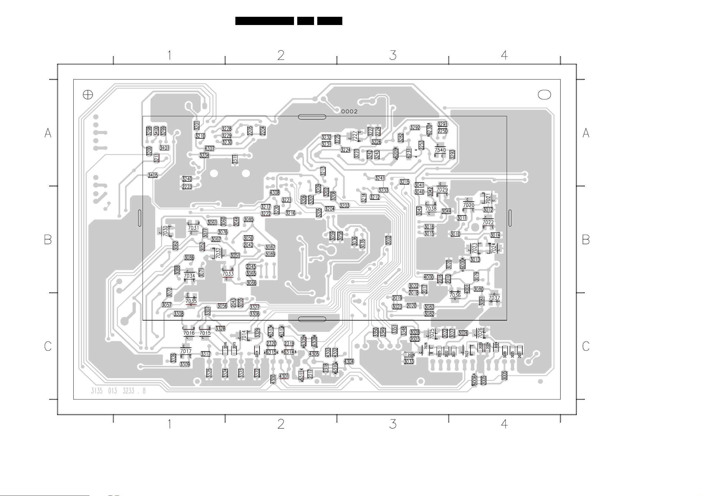
Circuit Diagrams and PWB Layouts
Layout ACS Panel (Bottom Side)
64DPTV465 7.
3135 013 3233.3
E_15000_041.eps
111004
2002 B3
2005 C4
2010 B3
2016 B3
2017 B3
2018 B3
2019 C3
2020 C3
2021 C4
2022 C3
2023 C3
2024 C4
2025 C3
2026 C3
2042 B2
2043 C2
2044 B2
2045 B2
2204 A2
2205 A2
2223 B1
2224 A3
2250 A3
2253 A3
2311 A2
2317 C2
2318 C2
2319 C2
2320 C2
3005 C4
3010 B4
3011 B4
3012 B4
3013 B4
3014 B4
3015 B3
3016 B3
3020 B4
3022 B3
3023 C3
3024 C4
3025 C4
3026 C4
3027 C4
3028 C3
3029 C4
3030 C4
3031 C4
3032 C3
3033 C3
3035 B3
3036 B3
3040 B3
3041 A3
3042 B3
3043 B3
3044 B3
3050 B2
3051 B2
3052 B1
3055 C2
3056 C1
3057 C1
3058 B3
3059 B2
3060 B1
3061 B1
3062 B1
3065 B2
3066 B2
3067 B1
3071 B1
3072 B1
3076 B1
3077 B1
3079 B4
3080 B4
3081 C4
3082 C3
3083 C3
3085 B2
3086 B1
3087 B2
3088 B1
3089 B2
3200 A1
3201 A1
3202 B2
3203 B3
3204 B2
3205 B2
3206 B2
3207 B2
3208 B2
3209 B2
3210 A1
3211 A1
3212 B3
3213 A2
3214 B3
3215 A3
3216 B2
3217 B2
3220 B2
3221 B2
3222 B2
3223 A3
3224 A3
3225 A3
3226 A3
3227 A3
3228 A2
3229 A2
3230 A2
3231 A2
3232 A2
3233 B3
3234 A1
3240 A1
3241 A3
3242 A3
3243 A3
3282 A3
3291 A3
3292 A3
3293 A4
3298 A1
3299 A1
3306 C2
3307 C1
3308 C1
3309 C1
3314 C2
3315 C2
3316 C2
3317 C1
3322 C2
3323 C2
3324 C1
3325 C1
3326 C1
3327 C2
3328 C1
3329 C2
3348 C3
3349 C3
3350 C3
3351 C3
3400 A1
3401 A1
3405 A1
4000 B3
4001 B4
4300 C2
4301 C2
4302 C2
4303 C2
4304 C3
4305 C2
4307 A1
4308 B2
6000 B4
6006 C4
6209 A3
6230 A3
6231 A3
6308 C2
6309 C2
6310 C2
6311 C2
6312 C2
6313 C2
6314 C2
6315 C2
7014 C2
7015 C1
7016 C1
7017 C1
7020 B4
7021 B4
7022 B4
7023 B4
7024 B4
7025 C3
7026 C4
7027 C4
7028 C3
7029 B3
7030 B1
7031 B1
7032 B1
7033 B2
7034 B1
7035 C1
7036 C4
7037 C4
7038 B3
7227 A3
7540 A3
Page 65
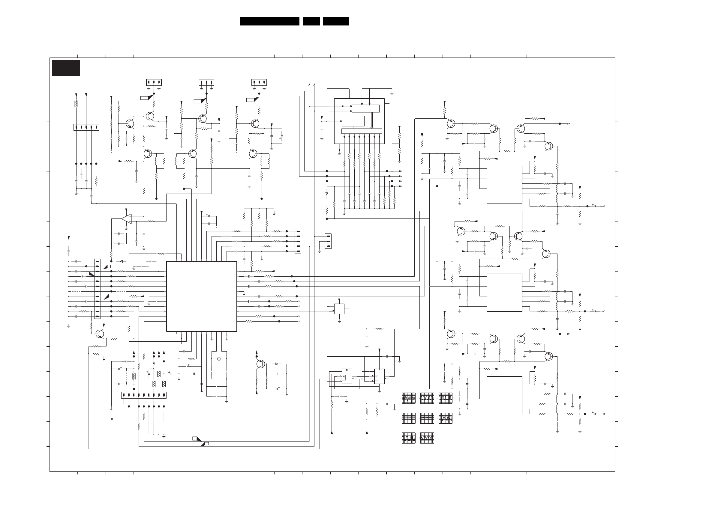
HOP Panel
J1
Circuit Diagrams and PWB Layouts
65DPTV465 7.
15K
3410
F410
5K6
3411
15K
3430
F430
16
5K6
3431
15K
3450
16
F450
5K6
3451
E_15000_042.eps
20
2410
2-J9
BPb
47u
2430
2-I9
GY
47u
2450
2-I9
RPr
47u
191004
1
J1
A
B
To Blue
CRT Panel
1701
C
D
E
F F
G
H
I
J
L
M
N
O
P
EH-B
+8V
2913
3135 033 3429.2
12
2
3 11
4
5
HDR2K4 HOP 28KHZ AP AUG
EH-B1720
123
BV1
3726
100R
7721
BF550
3723
1K0
1K2
3722
7720
3721
820n
5721
1u0
3720
100R
10K
3903
F642
3902
10K
1u0
2933
1u0
3643
100R
2601
2602
1n0
1n0
+8V
2607
47n
-12V
3965
100R
F963
F952
S1D
6963
100R
16
3952
47u
2963
1R0
1R0
3953
3951
F967
F966
F958
F955
4.9V
9.1V
4.9V
11.9V
3955
100R
100n
2953
2951
100R
2952
To Green
CRT Panel
1210
+8V
39K
3715
-8V
22K
3714
2721
100n
2714
100n
3711
680R
5711
820n
680R
3710
100R
F641
44
42
43
BO
BCL
BLKIN
1
VDOA
2
VDOB
3
EWO
4
EHTIN
5
FLASH
6
GND1
7
DECVD
8
HOUT
9
SCO
10
SCL
11
SDA
HFB
HSEL
DPC
13
12
14
2615
100n
3616
47u
To SSM
Panel
1950
39K
2616
47u
F951
2961
1R0
16
1R0
1950
JL
9
F959
12V
100n
100n
+8V +12V
3750
1
F750
2740
2750
1n0
2901
1u0
2903
2904
10p
2905
1n0
4907
2910
10p
2912
100n
1R0
2
F740
100n
10p
3911
47K
345
F730
100n
2702
2644
To LSP
1510
1.5V
F902
.7V
F3
4.3V
2906
1n0
2909
2.9V
10p
.6V
4V
3617
To Blue
CRT Panel
1210
+8V
4K7
39K
3732
3725
1K5
1u0
3731
2731
3727
220R
+12V
8
1
4
2911
1u0
2900
1u0
6643
BAS316
3601
3602
100R
3603
100R
100R
3604
100R
4605
3608
3609
47R
100R
3613
2K2
3614
2968
100n
4957
2957
100n
2345678
1
F962
7730
BF550
1K2
3730
BF570
2720
3
2
2902
3607
1K0
100R
+5V
F957
3966
3957
F961
F954
3956
22K
3724
2724
100n
F644
F760
3644
100n
100p
1510
EH-B
1V
1K0
3619
1K0
3620
1K0
+8V
1K0
7900-1
LM393D
18K
3901
1
F901
2
F2
F903
3
F904
4
.7V
F905
5
F906
6
F907
7
8
L2
F909
9
F910
10
F911
11
F912
12
+12V
7601
BC847B
3618
1K0
2958
47u
2-L1
Hf
3456
+12V
1K0
3426
7413
BF550
2473
SHARP
F802
SREF
2483
SHARP
+12V
3466
7453
BF550
SREF
2493
SHARP
C2
2V / div AC
20µs / div
GV1
200mV / div AC
10µs / div
15
3427
390R
+12V
1K0
3470
100n
1K0
3471
1n0
2470
7433
BF550
+12V
1K0
3480
100n
1K0
3481
1n0
2480
1K0
3467
390R
+12V
1K0
3490
100n
1K0
3491
1n0
2490
15
16
3429
180R
7412
BF550
3424
390R
3p3
2424
2409
100n
3425
470R
+CARRIER
8
NC4
2471
2472
3441
1K0
2481
2482
2491
2492
13
100n
-CARRIER
10
NC3
11
-OUTPUT
12
NC2
1n0
9
VEE
14
+12V
3443
100R
7432
BF550
3444
390R
3p3
2444
2429
100n
3445
470R
+CARRIER
8
NC4
100n
13
-CARRIER
10
NC3
11
-OUTPUT
12
NC2
1n0
9
VEE
14
3460
180R
7452
BF550
3464
390R
3p3
2464
2449
100n
3465
470R
+CARRIER
8
NC4
13
100n
-CARRIER
10
NC3
11
-OUTPUT
12
NC2
1n0
9
VEE
14
16
17
1K0
22R
3420
3422
3428
220R
+12V
NC1
+OUTPUT
BIAS
7410
MC1496D
-SIG_INP
GAIN_ADJ2
GAIN_ADJ1
+SIG_INP
3449
180R
3447
390R
22R
3448
3442
220R
+12V
NC1
+OUTPUT
BIAS
7430
MC1496D
-SIG_INP
GAIN_ADJ2
GAIN_ADJ1
+SIG_INP
1K0
22R
3468
3463
3462
220R
+12V
NC1
+OUTPUT
BIAS
7450
MC1496D
-SIG_INP
GAIN_ADJ2
GAIN_ADJ1
+SIG_INP
1714 20
7
6
5
4
3
2
1
7434
BF550
7
6
5
4
3
2
1
7
6
5
4
3
2
1
7414
BF550
2439
10p
7454
BF550
18
3421
+12V
1K0
3419
430R
2419
10p
7411
BF570
+12V
3K9
3416
2416
100n
3415
22R
3414
100R
3413
22R
3446
+12V
1K0
3439
430R
7431
BF570
+12V
3K9
3436
2436
100n
3435
22R
3434
100R
3433
22R
3461
+12V
1K0
3459
430R
2459
10p
7451
BF570
+12V
3K9
3456
2456
100n
3455
22R
3454
100R
3453
22R
18
19
2-E3
VV
F414
22R
3418
2422
120p
2u7
5411
2421
47p
560n
5410
3412
180R
4p7
2420
22R
3438
2442
120p
2u7
5431
2441
47p
5430
560n
3432
180R
4p7
2440
2-A4
UU
F454
22R
3458
2462
120p
2u7
5451
2461
47p
5450
560n
3452
180R
4p7
2460
+12V
+12V
+12V
12
5A06
A1
I2C BUS
SLAVE RECEIVER
DAC0-7
DAC312
11 DAC2
13 DAC4
14 DAC5
1K0
1K0
3811
100n
2811
10K
3814
3812
15K
1K0
3813
3815
2812
100n
2814
100n
2815
100n
2813
100n
2608
100p
15
14
11
6
12
7
13
4K7
3629
12
13
NC
+12V
100K
100K
TINT
VS1
VS2
SYNCSEL
BV1
200mV / div AC
10µs / div
1V / div AC
10µs / div
L2
2V / div AC
10µs / div
+12V
1K0
3801
1K0
3802
C1
2V / div AC
5µs / div
F3F2
1V / div AC
10µs / div
RV1
200mV / div AC
10µs / div
SREF
1u0
2802
3818
15 DAC6
CX
RCX
R
3625
16 DAC7
3816
10K
2816
100n
3621
180R
+5V
168
10K
F813
100n
3824
2605
100n
7605-2
74HC4538D
2604
820p
240K
3817
2-H7,2-D7
F814
2-A15
2-L12
F815
F816
2-J3
10K
3825
10K
10K
3826
10
9
13
B-BIAS
2-C8
2-K1
2-L1
109
SCL
SDA
2-A15
2-A15
U
V
HD
VD
SDA
SCL
7800
TDA8444T/N4
3
SDA
4
SCL
+12V
2
VMAX
2800
100n
GND
8
F809
F810
F811
6495
BAS316
3496
100K
22K
3495
F812
1030
JQ-S
1
2
3
+5V
7602
74AHC1G66GV
1
1
4
X1
35
7605-1
74HC4538D
1
2
5
4
3
2603
820p
6K2
3611
+5V +5V
11
1
VP
REFERENCE
VOLTAGE
GENERATOR
9DAC0
10 DAC1
3810
1K0
3809
2810
100n
2809
SHARP
2
1
168
CX
RCX
R
NOTES
1. CAPACITANCE VALUES ARE IN FARADS:
m=MILI u=MICRO n=NANO p=PICO f=FEMTO
2. RESISTANCE VALUES ARE IN OHMS:
R=OHM K=KILO M=MEGA G=GIGA T=TERA
3. SAFETY TRIANGE REPRESENTS PCEC REPLACEMENT PART ONLY.
4. FOR VALUE SEE TABLE.
*
6
EH-B1710
123
F712
GV1
3716
100R
7711
BF550
3713
1K0
+8V
1K2
3712
3707
7710
BF570
3708
1u0
2710
+8V
2638
47u
16
2639
100n
38
39
40
41
GO
VSC
15
2617
22n
F616
RO
VP2
7600
TDA9331H
VP1
IREF
16
17
+8V
BL2
DECBG
18
2620
37
BI2
GND2
19
75R
47R
DSX840
12p
2618
2u2
2619
22n
-8V
2711
36
GI2
XTALI21XTALO
20
1601
12M
100n
35
RI2
2637
100n
2635
100n
2621
34
PWL
FBCSO
DACOUT
LPSU
22
12p
7
To Red
CRT Panel
1210
+8V
39K
3705
22K
3704
100n
2704
3639
100R
2636
100n
2634
22n
33
BL1
32
BI1
31
GI1
30
RI1
29
28
YIN
27
UIN
26
VIN
25
24
HD
23
VD
8 14
EH-B1700
123
BF570
3645
2633
7700
BC807-25
F702F722
RV1
3706
100R
-8V
7701
BF550
3703
1K0
2701
1K2
3702
3701
820n
5701
1u0
3700
100R
2700
F640
3647
100R
100R
10K
3648
3646
100R
3637
47R
3635
47R
1u0
1K0
3633
3634
2632
100n
2630
100n
2627
100n
3623
100R
3632
1K0
2631
10R
3630
100n
10R
2628
F627
100n
2626
F626
100n
3624
F624
100R
-8V+8V +12V
F956
7922
BZX284-C6V8
1K0
10R
3923
3922
-12V
G-BIAS
R-BIAS
47u
2924
100n
16
680R
3638
47R
3636
47R
+8V
F623
6923
2923
1u0
2922
47u
1610
F615
5
F614
4
F613
3
F612
2
F611
1
EH-B
To SSM
Panel
1610
F632
3631
F631
10R
F630
3628
F628
10R
3627
3626
10R
2-G8
10R
C2
C1
7
8 19
910
A
B
C
D
E
G
H
I
J
KK
L
M
N
O
P
Page 66
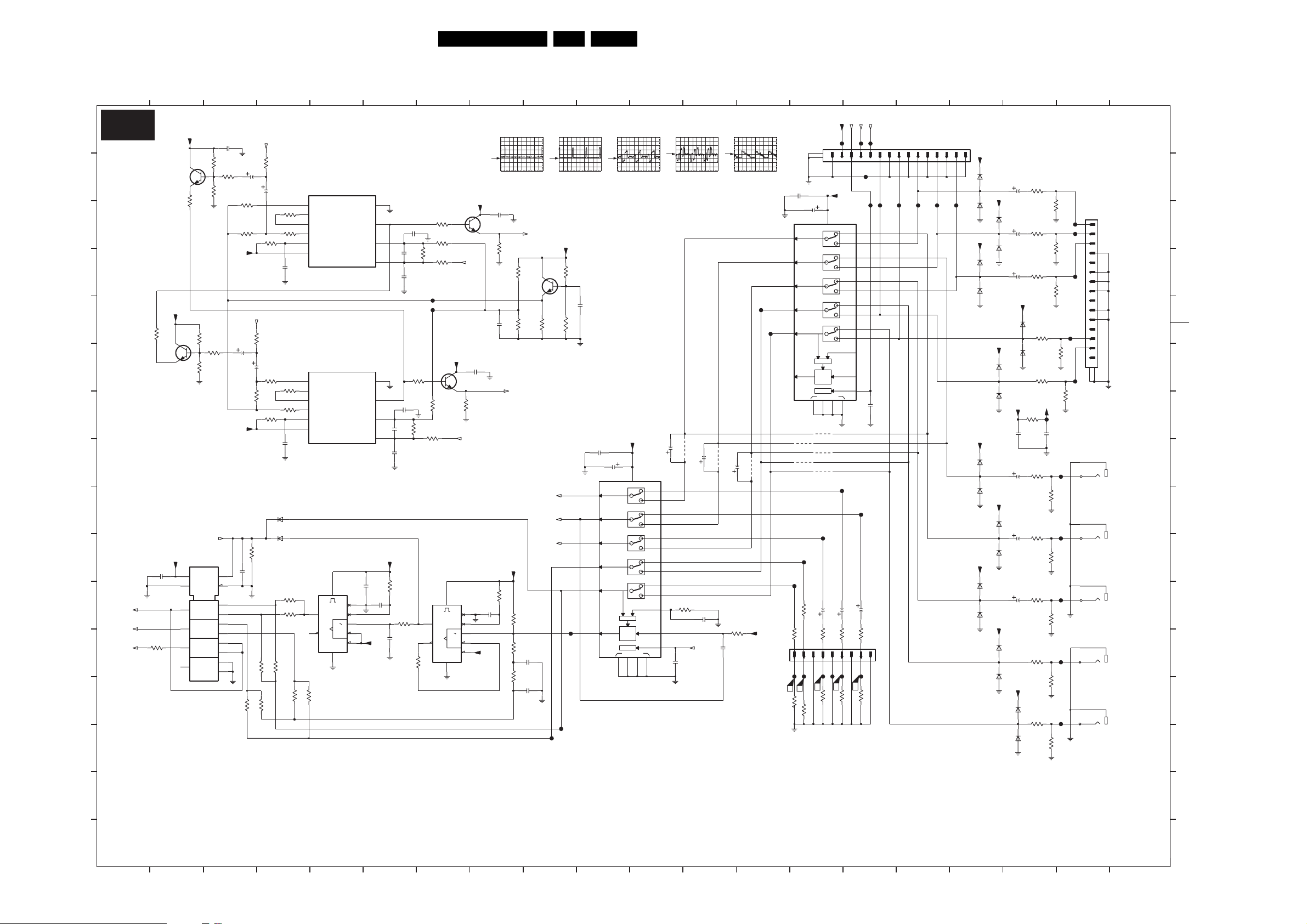
HOP Panel
J2
Circuit Diagrams and PWB Layouts
66DPTV465 7.
47u
2520
3331
100n
VOUT2
VV
1-C19
3520
3526
100R
4
UU
1-K19
10R
3510
47u
2510
3519
3K9
10R
47u
3525
22R
1K0
3529
3K9
6341
BAS316
6331
BAS316
1M0
3332
3343
100R
3345
100R
HOUT2
100R
+SIG_INP
1
3517
GAIN_ADJ1
2
470R
GAIN_ADJ2
3
3518
4
22R
5
6
7
2519
100n
1
3527
2
470R
3
3528
4
22R
5
6
7
100n
2529
3342
100R
3333
100R
-SIG_INP
BIAS
+OUTPUT
NC1
+SIG_INP
GAIN_ADJ1
GAIN_ADJ2
-SIG_INP
BIAS
+OUTPUT
NC1
10
9
16
7510
MC1496D
7520
MC1496D
CX
RCX
>
1
R
8
3336
100R
3346
100R
-OUTPUT
-CARRIER
+CARRIER
-OUTPUT
-CARRIER
+CARRIER
15
14
12
11
13
7328-B
74HC4538D
14
VEE
9
NC2
12
11
NC3
10
13
NC4
VEE
NC2
NC3
NC4
2329
2502
8
2500
14
9
12
2506
11
1n0
10
13
100n
2507
8
1n0
2505
2K2
3325
100n
2325
470p
3326
1K0
68p
2326
+5V
1
A
J2
B
C
HDR2K4 HOP 28KHZ ( AP)
BF570
+12V
7511
3530
330R
2509
100n
1K8
3513
3512
2511
3511
22R
15K
3515
TREF
22R
3516
1K0
+12V
D
+12V
3540
330R
7521
BF570
F
1K8
3523
3522
2521
3521
22R
15K
47u
TREF
G
+12V
H
I
1-E13
SYNCSEL
J
K
L
1-J9
HD
1-K9
VD
1-N3
3339
Hf
1K0
M
7330
+5V +5V
74HC157D
2330
100n
4
7
9
12
VCC
GND
MUX 1~
116
2331
G1
158
EN
2
3
1
5
6
11
10
14
13
3335
N
76
3531
2501
22R
3501
1n0
22R
3502
220R
100n
1n0
3541
22R
3507
3323
1-E13,2-H7
3500
22R
F805
F807
TBIAS
+12V
7540
BF570
22R
3506
220R
3505
22R
62
1-E13,2-D7
16
RCX
3542
TINT
CX
>
1
R
2K2
8
74HC4538D
TINT
1
4
57
3
7328-A
+5VA
6122
6121
+5VA
6147
6146
+5VA
6162
6161
+5VA
6182
6181
BAS316
BAS316
BAS316
BAS316
BAS316
BAS316
BAS316
BAS316
+5VA
181716152 10
2019
A
2110
3111
47R
47u
2120
47u
2130
47u
+5VA
6142
6141
+5V
3944
10R
100n
2944
2150
47u
2160
47u
2170
47u
6187
BAS316
6186
BAS316
3121
47R
3131
47R
BAS316
BAS316
3151
47R
3161
47R
3171
47R
3181
220R
3186
220R
220R
220R
75R
3110
3120
3130
3141
3146
+5VA
F953
2945
100n
3150
3160
3170
31803185
1110
SUB-D
1
F111
2
F112
3
4
75R
5
6
F113
7
8
75R
9
10
11
12
F114
13
14
15
1K0
3140
16 17
F115
1K0
3145
1150-A
2
YKC21
F152
1
75R
1150-B
YKC21
4
F162
3
75R
1150-C
6
YKC21
F172
5
75R
1180-A
YKC21
2
F182
1
1K0
1180-B
YKC21
4
F185
3
1K0
B
C
D
EE
F
G
H
I
J
K
L
M
N
10µs / div
+5V
20
VCC
DET
SYNC
SEPA
LOGIC
GROUND
BA7657F
R1-IN
1
R2-IN
2
G1-IN
1
G2-IN
2
B1-IN
1
B2-IN
2
VD1-IN
1
VD2-IN
2
HD1-IN
1
HD2-IN
2
HD-S-SIG-DET
4
6810
11
7210
V15
200mV / div AC
2210
47u
1
7
3
9
5
11
12
13
24
23
3248
2
470K
16CTL
2216
10µs / div
4210
2248
470p
1-E13
VS2
100n
2220
47u
4220
2247
8
F1
2V / div AC
2ms / div
+12V
2806
1n0
7530
BF570
3K3
3532
TREF
1u0
2807
2931
1n0
1-J9
V
3K3
+5V
68K
3324
2324
470p
3320
3321
+5V
3322
953
L1
2V / div AC
10µs / div
1-J9
U
+12V
4K7
3806
7805
BC847B
4K7
3807
3805
2K2
CSO
4K7
2321
470p
4K7
2322
470p
4K7
3803
2804
3K
1K0
3804
1-N20
RPr
1-J20
GY
1-F20
BPb
VOUT2
HOUT2
F217
F222
F214
V11
200mV / div AC
1u0
2291
100n
2290
47u
21 R-OUT
19 G-OUT
B-OUT15
14 VD-OUT
HD-OUT22
C-S-OUT17 18C-V-IN
1312
V18
500mV / div AC
10µs / div
F201
2230
47u
4230
VOUT1
HOUT1
3247
+5V
68K
2u2
To SSM
Panel 1250
2191
100n
R-OUT21
G-OUT19
15 B-OUT
14
VD-OUT
VOUT1
F202
22 HD-OUT
HOUT1
17 C-S-OUT C-V-IN 18
4221
4213
F281
F286
3281
3286
220R
.6V
.05V
1250
JL
123456789
F252
F251
L1
F1
1K0
3285
3280
14
2190
47u
220R
1K0
17
16
20
VCC
DET
SYNC
SEPA
LOGIC
GROUND
4211
4231
4223
F270
2270
3271
7.5V
F254
V15
3270
+5V
F014
15
+5V
BA7657F
R1-IN
1
R2-IN
2
G1-IN
1
G2-IN
2
B1-IN
1
B2-IN
2
VD1-IN
1
VD2-IN
2
HD1-IN
1
HD2-IN
2
HD-S-SIG-DET
46810
F260
47u
2260
47R
3261
7.4V
F255
V11
75R
3260
VS1
14
7110
CTL 16
47u
47R
F256
75R
SDA
SCL
1-E13
1-A10
1-A10
F012
F011
12
13
10
11
F015
F006
F008
F010
F013
1
7
3
9
5
11
12
13
24
23
2
2111
100n
F250
47u
2250
47R
3251
1111
JET
+5VA
2
3456789
1
6112
BAS316
F002
F004
+5VA
+5VA
+5VA
6111
BAS316
6132
BAS316
6131
BAS316
6152
BAS316
6151
BAS316
6172
BAS316
6171
BAS316
1.6V
F258
V18
75R
3250
O
P
3135 033 3429.2
1
O
P
E_15000_043.eps
141004
3
6
891045 15
11
127
13
142
16 17 18 19
20
Page 67
Circuit Diagrams and PWB Layouts
J3
Diversity HOP Panel J1 and J2
67DPTV465 7.
1
HDR2K4 HOP 28KHZ AP AUG
A
J3
N3 HOP DB15 N3 HOP W/O DB15
Ref Des 3135_037_12781_01 3135_037_12791_01 RESERVED
1030 NOT USED NOT USED 242202517535
NOT USED NOT USED NOT USED
2603
B
2604 NOT USED NOT USED NOT USED
2605 NOT USED NOT USED
2608 NOT USED NOT USED NOT USED
2900 NOT USED NOT USED 319801721050
C
3611 NOT USED NOT USED NOT USED
3613 319802152220
2K2
3617
NOT USED NOT USED NOT USED
3618 NOT USED NOT USED NOT USED
D
E
F
G
NOT USED NOT USED NOT USED
3619
3620 NOT USED NOT USED NOT USED
3621 NOT USED NOT USED
3625 NOT USED NOT USED NOT USED
3629 NOT USED NOT USED
3816 NOT USED NOT USED 319802151030
3817 NOT USED NOT USED 319802151040
3818 NOT USED NOT USED
3826 NOT USED NOT USED 319802151030
4957 NOT USED
7601 NOT USED NOT USED NOT USED
7602 NOT USED NOT USED NOT USED
7605-1
NOT USED NOT USED NOT USED
7605-2 NOT USED NOT USED NOT USED
H
I
J
K
L
319802152220
2K2
NOT USED 319802190020
SHEET 1
RESERVED
JQ-S
NOT USED
1u0
NOT USED
NOT USED
NOT USED
10K
100K
319802151040
100K
10K
N3 HOP DB15 N3 HOP W/O DB15
Ref Des
1110 242202516857
SUB-D
1111 NOT USED NOT USED 242202517519
2110 319803044790
47u
2120 319803044790
47u
2130 319803044790
47u
2210 319803044790
47u
2220
319803044790
47u
2230 319803044790
47u
319802157590
3110
75R
3111 319802154790
47R
319802157590
3120
75R
3121 319802154790
47R
3130
319802157590
75R
3131 319802154790
47R
3140 319802151020
1K0
3141
319802152210
220R
3145 319802151020
1K0
3146
319802152210
220R
3250 NOT USED NOT USED 319802157590
3260
NOT USED NOT USED 319802157590
3270 NOT USED NOT USED 319802157590
3280 NOT USED NOT USED 319802151020
3285 NOT USED NOT USED 319802151020
3332 NOT USED NOT USED 319802151010
3333 NOT USED NOT USED
3335 NOT USED NOT USED 319802151010
3336 NOT USED
4210 NOT USED 319802190020 NOT USED
4211 NOT USED 319802190020
4213 NOT USED 319802190020 NOT USED
4220 NOT USED 319802190020 NOT USED
4221 NOT USED 319802190020 NOT USED
4223 NOT USED
4230 NOT USED 319802190020 NOT USED
4231 NOT USED 319802190020 NOT USED
319801010630
6111
BAS316
6112 319801010630
BAS316
319801010630
6121
BAS316
6122 319801010630
BAS316
319801010630
6131
BAS316
6132 319801010630
BAS316
6141 319801010630
BAS316
319801010630
6142
BAS316
6146 319801010630
BAS316
6147
319801010630
BAS316
6331 NOT USED NOT USED 319801010630
7110 932211562668
BA7657F
3135_037_12791_013135_037_12781_01
NOT USED NOT USED
NOT USED NOT USED
NOT USED NOT USED
NOT USED NOT USED
NOT USED NOT USED
NOT USED NOT USED
NOT USED NOT USED
NOT USED
NOT USED NOT USED
NOT USED NOT USED
NOT USED NOT USED
NOT USED NOT USED
NOT USED
NOT USED NOT USED
NOT USED NOT USED
NOT USED NOT USED
NOT USED NOT USED
NOT USED 319802151010
319802190020 NOT USED
NOT USED NOT USED
NOT USED NOT USED
NOT USED NOT USED
NOT USED NOT USED
NOT USED NOT USED
NOT USED NOT USED
NOT USED NOT USED
NOT USED
NOT USED NOT USED
NOT USED NOT USED
NOT USED
RESERVED
RESERVED
JET
NOT USED
NOT USED
75R
75R
75R
1K0
1K0
100R
319802151010
100R
100R
100R
NOT USED
NOT USED
BAS316
NOT USED
SHEET 2
765432
Personal Notes:
A
B
C
D
E
F
G
H
I
J
K
L
M
N
O
P
3135 033 3429.2
12345
M
N
O
P
E_15000_044.eps
191004
67
E_06532_012.eps
131004
Page 68
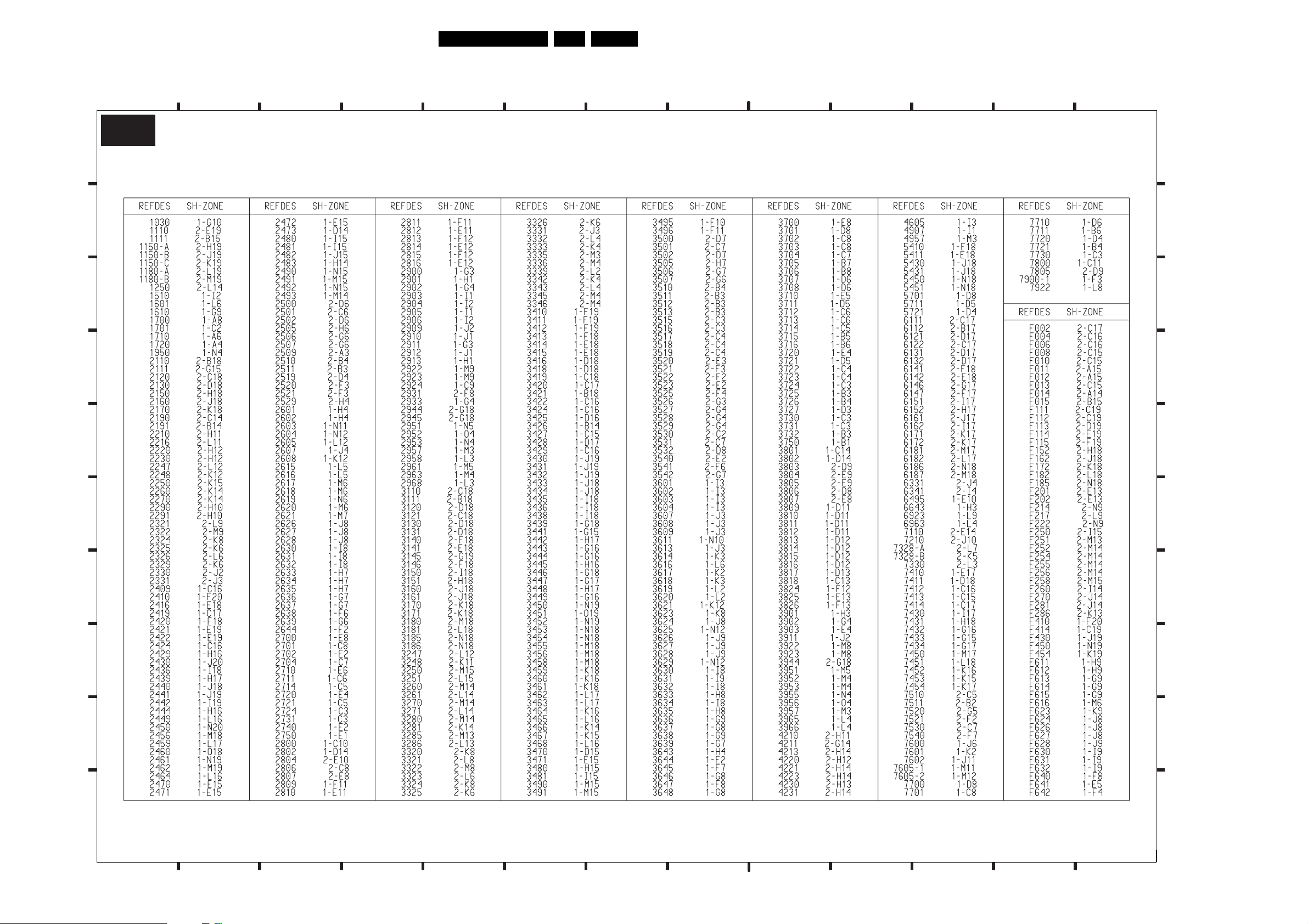
Circuit Diagrams and PWB Layouts
J4
Mapping HOP Panel J1 and J2 Part 1
68DPTV465 7.
A
B
C
D
J4
HDR2K4 HOP 28KHZ AP AUG
54321
6
7
1312111098
A
B
C
D
E
G
H
E
F
I
F
G
H
I
J
3135 033 3429.2
1
65432 1312111098
7
E_15000_045.eps
111004
J
Page 69
Circuit Diagrams and PWB Layouts
J5
Mapping HOP Panel J1 and J2 Part 2
69DPTV465 7.
Personal Notes:
4321
A
B
C
D
E
J5
HDR2K4 HOP 28KHZ AP AUG
A
B
C
D
E
G
H
F
F
G
H
I
J
I
J
3135 033 3429.2
1432
E_15000_046.eps
191004
E_06532_012.eps
131004
Page 70
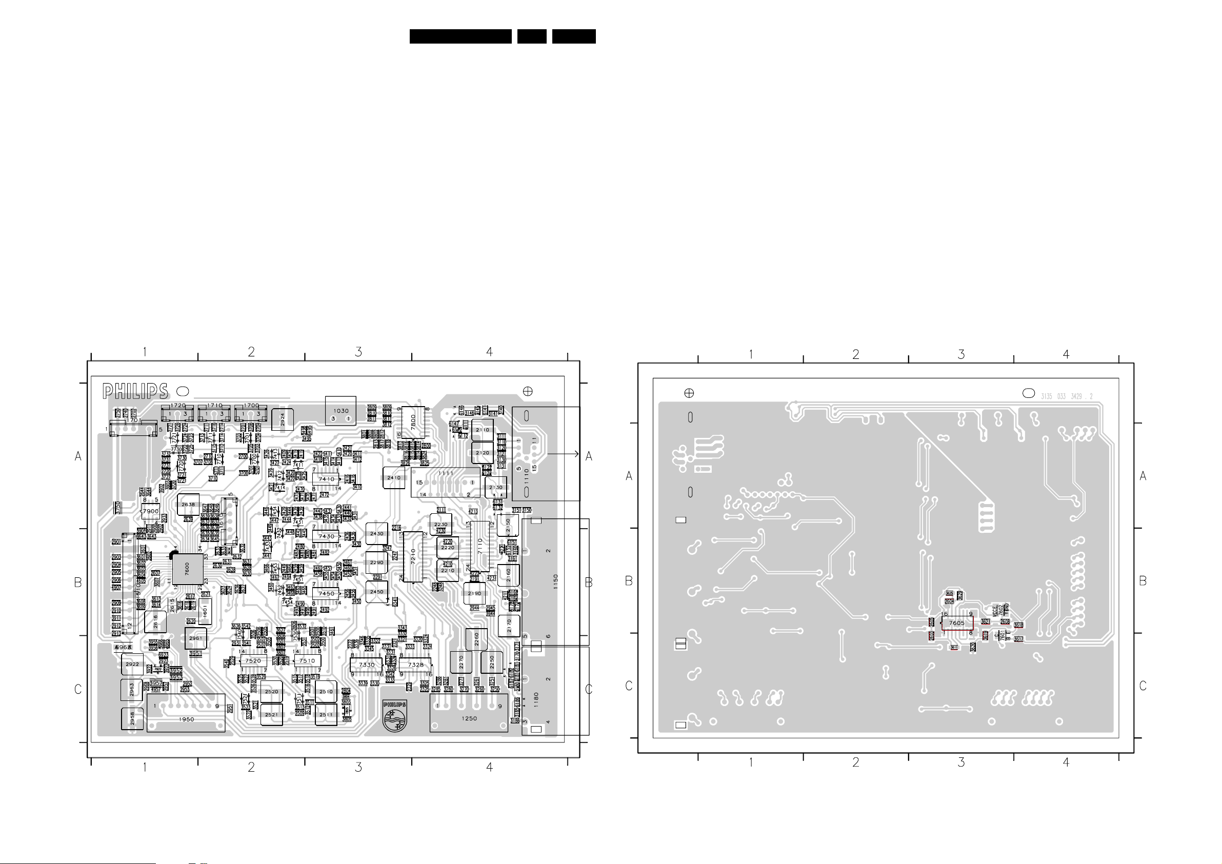
Circuit Diagrams and PWB Layouts
70DPTV465 7.
Layout HOP Panel (Top Side)
2816 A3
2638 A1
2509 C2
2442 A3
2248 B4
1030 A3
1110 A4
1111 A4
1150 B4
1180 C4
1250 C4
1510 B1
1601 B2
1610 A2
1700 A2
1701 A1
1710 A2
1720 A1
1950 C1
2110 A4
2111 A4
2120 A4
2130 A4
2150 A4
2160 B4
2170 B4
2190 B4
2191 B4
2210 B4
2216 A3
2220 B4
2230 A4
2247 B3
2250 C4
2260 C4
2270 C4
2290 B3
2291 B3
2321 C3
2322 C3
2324 C4
2325 C4
2326 C3
2329 C3
2330 C3
2331 C3
2409 A2
2410 A3
2416 A3
2419 A2
2420 A3
2421 A3
2422 A3
2424 A2
2429 A2
2430 B3
2436 B3
2439 A2
2440 A3
2441 A3
2444 A2
2449 B2
2450 B3
2456 B3
2459 B2
2460 B3
2461 B3
2462 B3
2464 B2
2470 A2
2471 A3
2472 A3
2473 A2
2480 B2
2481 B3
2482 B3
2483 B2
2490 B2
2491 B3
2492 B3
2493 B2
2500 B3
2501 B3
2502 C3
2505 B2
2506 B2
2507 C2
2510 C3
2511 C3
2519 C2
2520 C2
2521 C2
2529 C2
2601 B1
2602 B1
2607 B1
2615 B1
2616 B1
2617 B1
2618 B1
2619 B1
2620 B1
2621 B2
2626 B2
2627 B2
2628 B2
2630 B2
2631 B2
2632 B2
2633 B2
2634 B2
2635 B2
2636 A2
2637 A2
2639 A1
2644 A1
2700 A2
2701 A2
2702 A1
2704 A2
2710 A2
2711 A2
2714 A2
2720 A1
2721 A1
2724 A1
2731 A1
2740 A1
2750 A1
2800 A4
2802 A3
2804 C3
2806 B2
2807 C2
2809 A3
2810 A3
2811 A3
2812 A3
2813 A3
2814 A4
2815 A4
2900 A1
2901 B1
2902 A1
2903 B1
2904 B1
2905 B1
2906 B1
2909 B1
2910 B1
2911 A1
2912 B1
2913 B1
2922 C1
2923 C1
2924 A2
2931 C2
2933 A1
2944 B4
2945 B4
2951 C2
2952 C1
2953 C1
2957 C1
2958 C1
2961 C1
2963 C1
2968 C1
3110 A4
3111 A4
3120 A4
3121 A4
3130 A4
3131 A4
3140 A4
3141 A4
3145 A4
3146 A4
3150 A4
3151 A4
3160 B4
3161 B4
3170 C4
3171 C4
3180 C4
3181 C4
3185 C4
3186 C4
3247 B3
3248 B4
3250 C4
3251 C4
3260 C4
3261 C4
3270 C4
3271 C4
3280 C4
3281 C4
3285 C4
3286 C4
3320 C4
3321 C3
3322 C3
3323 C3
3324 C4
3325 C4
3326 C3
3331 C3
3332 B3
3333 C3
3335 C3
3336 C3
3339 C3
3342 C3
3343 B3
3345 C3
3346 C3
3410 A3
3411 A3
3412 A3
3413 A3
3414 A3
3415 A3
3416 A3
3418 A3
3419 A2
3420 A2
3421 A2
3422 A2
3424 A2
3425 A2
3426 A2
3427 A2
3428 A2
3429 A2
3430 B3
3431 A3
3432 A3
3433 A3
3434 A3
3435 A3
3436 B3
3438 A3
3439 A2
3441 B2
3442 B2
3443 B2
3444 A2
3445 B2
3446 A2
3447 A2
3448 B2
3449 A2
3450 B3
3451 B3
3452 B3
3453 B3
3454 B3
3455 B3
3456 B3
3458 B3
3459 B2
3460 B2
3461 B3
3462 B2
3463 B2
3464 B2
3465 B2
3466 B2
3467 B2
3468 B2
3470 A3
3471 A2
3480 B3
3481 B2
3490 B3
3491 B2
3495 A3
3496 A2
3500 C3
3501 C2
3502 C3
3505 C2
3506 B2
3507 C2
3510 B3
3511 C3
3512 C3
3513 C2
3515 C2
3516 C3
3517 C2
3518 C3
3519 C3
3520 C2
3521 C2
3522 C2
3523 C2
3525 C2
3526 C2
3527 C2
3528 C2
3529 C2
3530 C2
3531 C2
3532 B2
3540 C2
3541 C2
3542 B2
3601 B1
3602 B1
3603 B1
3604 B1
3607 B1
3608 B1
3609 B1
3613 B1
3614 B1
3616 B1
3623 B2
3624 B2
3626 B2
3627 B2
3628 B2
3630 B2
3631 B2
3632 B2
3633 B2
3634 B2
3635 B2
3636 A2
3637 A2
3638 A2
3639 A2
3643 B1
3644 A1
3645 B2
3646 A2
3647 A2
3648 A2
3700 A2
3701 A2
3702 A2
3703 A2
3704 A2
3705 A2
3706 A2
3707 A2
3708 A2
3710 A2
3711 A2
3712 A2
3713 A2
3714 A2
3715 A2
3716 A2
3720 A1
3721 A1
3722 A1
3723 A1
3724 A1
3725 A1
3726 A1
3727 A1
3730 A1
3731 A1
3732 A1
3750 A1
3801 A3
3802 A3
3803 C3
3804 C3
3805 C3
3806 C2
3807 C2
3809 A3
3810 A3
3811 A3
3812 A3
3813 A3
3814 A4
3815 A4
3816 A3
3817 A3
3818 A3
3824 A4
3825 A4
3826 A3
3901 B1
3902 A1
3903 A1
3911 B1
3922 C1
3923 C1
3944 B4
3951 C1
3952 C1
3953 C1
3955 C1
3956 C1
3957 C1
3965 C1
3966 C1
4210 B4
4211 B4
4213 A4
4220 B4
4221 B4
4223 B4
4230 B4
4231 B4
4605 B1
4907 B1
4957 C1
5410 A3
5411 A3
5430 A3
5431 A3
5450 B3
5451 B3
5701 A2
5711 A2
5721 A1
6111 A4
6112 A4
6121 A4
6122 A4
6131 A4
6132 A4
6141 A4
6142 A4
6146 A4
6147 A4
6151 B4
6152 B4
6161 B4
6162 B4
6171 B4
6172 B4
6181 C4
6182 C4
6186 C4
6187 C4
6331 C3
6341 B3
6495 A3
6643 B1
6923 C1
6963 C1
7110 B4
7210 B4
7328 C4
7330 C3
7410 A3
7411 A2
7412 A2
7413 A2
7414 A2
7430 B3
7431 A2
7432 B2
7433 B2
7434 A2
7450 B3
7451 B2
7452 B2
7453 B2
7454 B2
7510 C3
7511 C2
7520 C2
7521 C2
7530 C2
7540 B2
7600 B1
7700 A2
7701 A2
7710 A2
7711 A2
7720 A1
7721 A1
7730 A1
7800 A4
7805 C3
7900 A1
7922 C1
Layout HOP Panel (Bottom Side)
2603 C3 2604 B3 2605 B3 2608 B3 3611 C3 3617 C4 3618 B4 3619 C3 3620 C3 3621 B3 3625 B3 3629 B3 7601 C3 7602 B3 7605 B3
3135 033 3429.2
E_15000_047.eps
141004
3135 033 3429.2
E_15000_048.eps
111004
Page 71
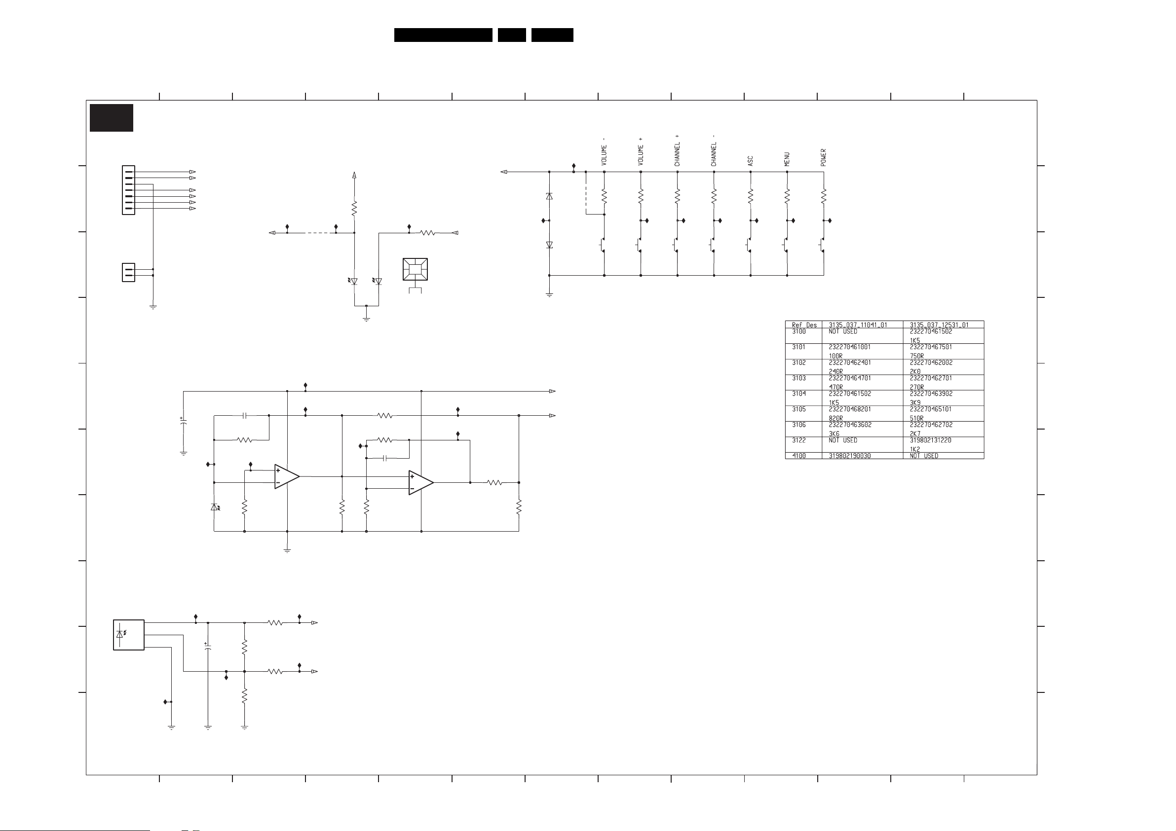
Keyboard Panel
K1
Circuit Diagrams and PWB Layouts
71DPTV465 7.
A
C
D
E
1
2
53
6
7
8
94
10
1211
13
KEYBOARD/LIGHT SENSOR AP
K1
A
6102
BZX284-C6V8
6103
BZX284-C6V8
+9V
LIGHT_SENSOR
I020
4100
1K5
3100
SKQNAB
1401
3101
100R
I014 I015
SKQNAB
1402
3102
240R
SKQNAB
1403
3103
470R
SKQNAB
1404
I016
1K5
SKQNAB
1405
3104
I017
3105
820R
I018 I019
SKQNAB
1406
3K6
3106
SKQNAB
1407
EMG STAR PEMG
BB
C
D
E
F
1201
1
2
3
4
5
6
7
S7B-EH
1202
1
2
106957
F
2101
10u 16V
+5V_STANDBY
KEYBOARD
+9V
ON_OFF_LED
LIGHT_SENSOR
RC5
I006
ON_OFF_LED
2102
470n
3110
1M5
I009
I021
4120
I007
I008 I012
7000-1
84
3
2
LM358DR2
1
I022
1K2
ORANGE-RED6101-1
I010
+5V_STANDBY
3122
TLUV5300
GREEN
6101-2
3111
10K
3112
3K3
2104
470n
TLUV5300
5
6
I024
3121
560R
1301
LED-HOLDER
84
7000-2
LM358DR2
7
KEYBOARD
I013
+9V
I011
3113
4K7
3K3
3118
G
G
BPW46
6104
1M5
3115
3K3
3116
1K0
3117
H H
6105
TSOP1736UU1
I
J
3135 033 3343.4
1
OUT
GND
2
VS
VS
3
OUT
1
GND
I005
I001 I002
2103
100u 16V
I004
2
6K8
10K
3108
3114
3
3107
330R
3109
470R
I003
+5V_STANDBY
RC5
49
5
6
7
8
NOTES
1. CAPACITANCE VALUES ARE IN FARADS:
m=MILI u=MICRO n=NANO p=PICO f=FEMTO
2. RESISTANCE VALUES ARE IN OHMS:
R=OHM K=KILO M=MEGA G=GIGA T=TERA
3. SAFETY TRIANGLE REPRESENTS PCEC REPLACEMENT PART ONLY.
4. FOR VALUE SEE TABLE.
10 12
11 13
E_15000_049.eps
191004
I
J
Page 72
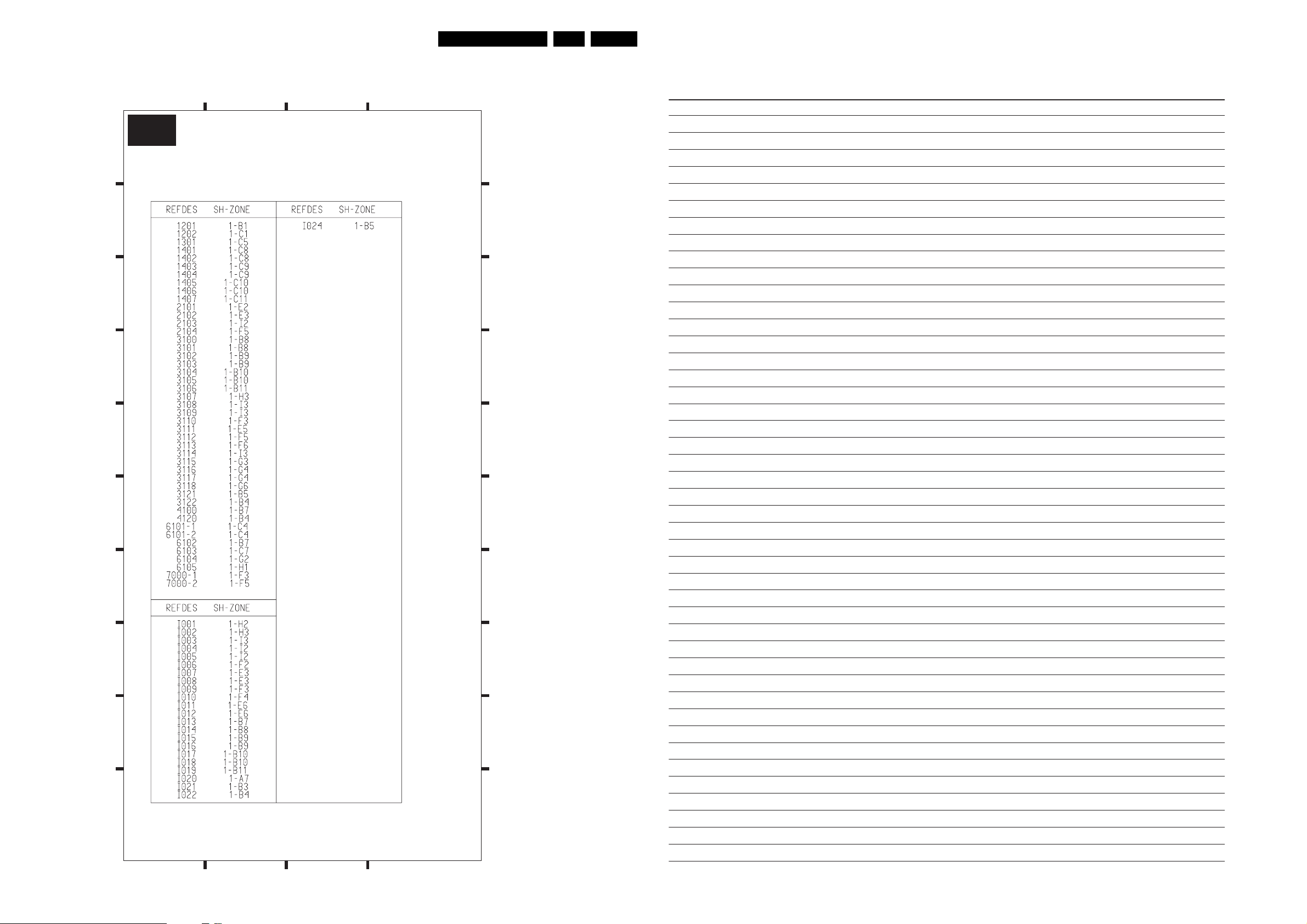
Circuit Diagrams and PWB Layouts
K2
Mapping Keyboard Panel
72DPTV465 7.
Personal Notes:
321
4
C
D
A
B
E
K2
KEYBOARD/LIGHT SENSOR AP
A
B
C
D
E
G
H
F
F
G
H
I
J
I
J
3135 033 3343.4
14
E_15000_050.eps
191004
E_06532_012.eps
131004
32
Page 73
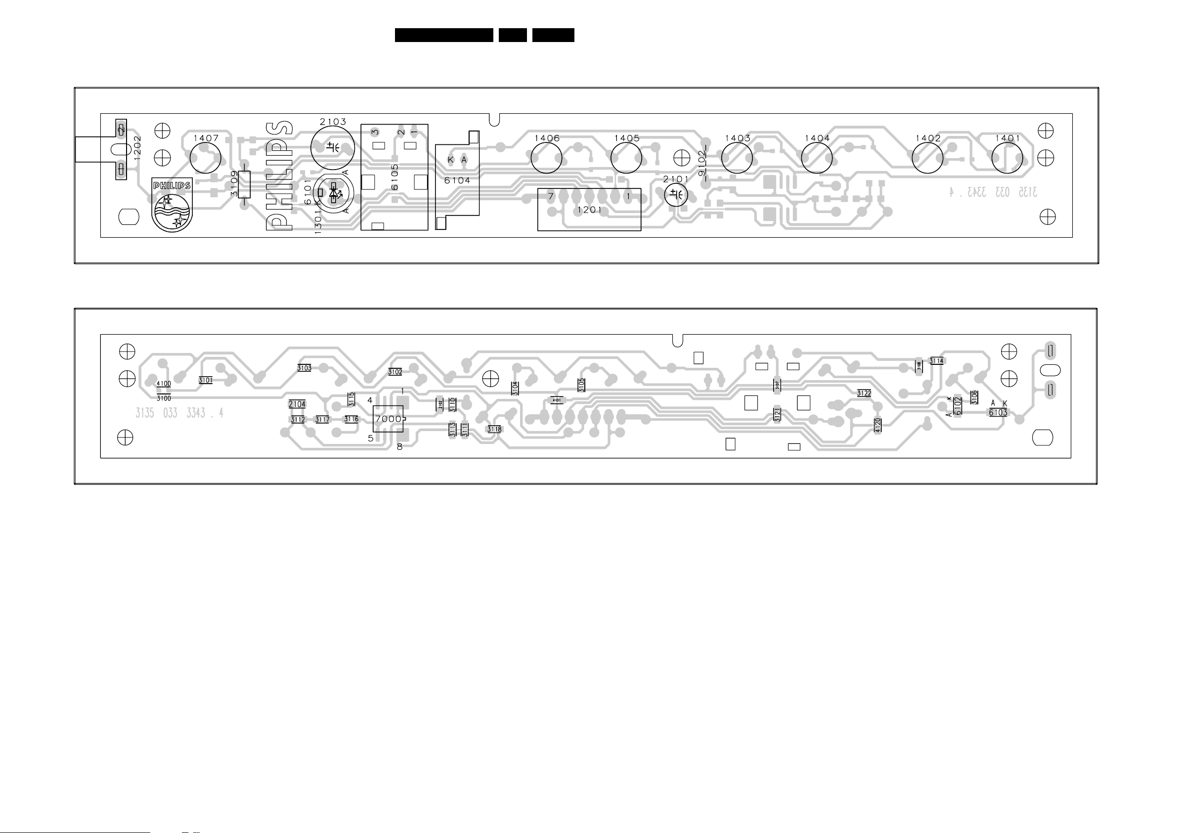
Circuit Diagrams and PWB Layouts
73DPTV465 7.
Layout Keyboard Panel (Top and BottomSide)
1201 -- 1202 -- 1301 -- 1401 -- 1402 -- 1403 -- 1404 -- 1405 -- 1406 -- 1407 -- 2101 -- 2103 -- 3109 -- 6101 -- 6104 -- 6105 -- 9102 --
3135 033 3343.4
2102 -2104 --
3100 -3101 --
3135 033 3343.4
3102 -3103 --
3104 -3105 --
3106 -3107 --
3108 -3110 --
3111 -3112 --
3113 -3114 --
3115 -3116 --
3117 -3118 --
3121 -3122 --
4100 -4101 --
4120 -6102 --
6103 -7000 --
E_15000_051.eps
111004
Page 74
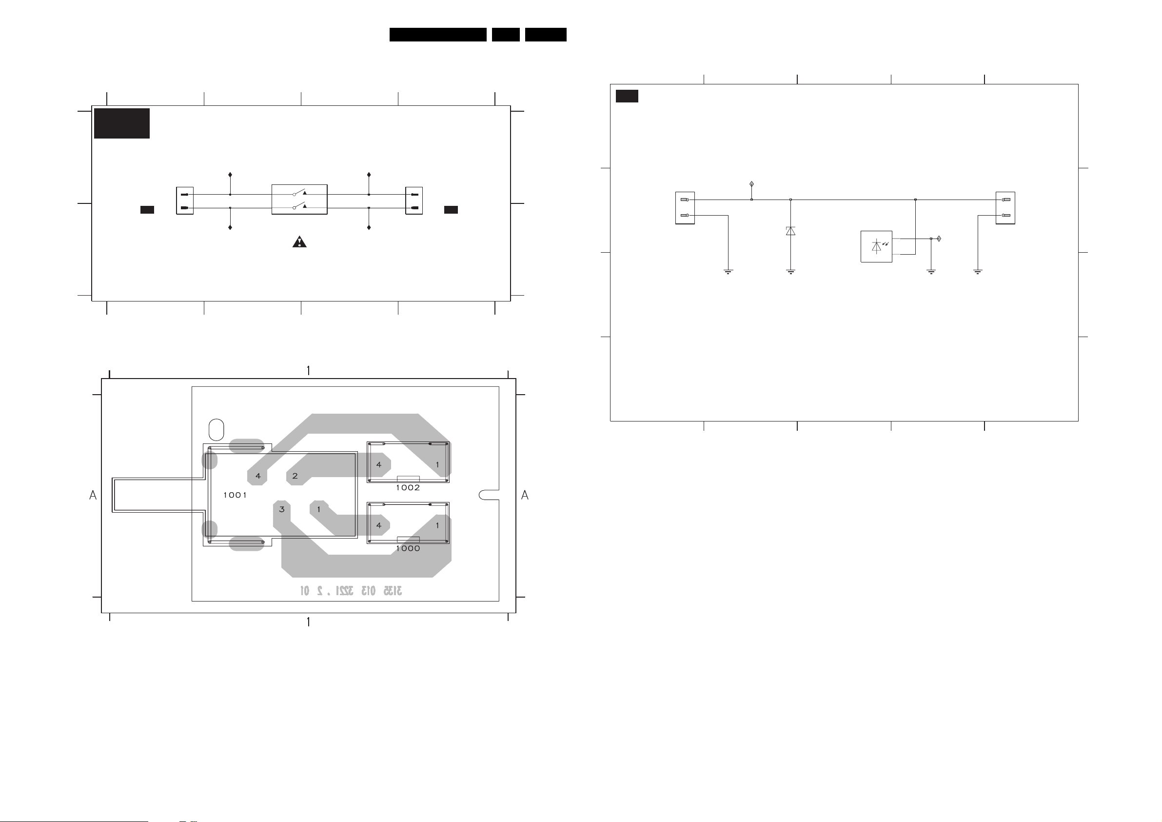
Circuit Diagrams and PWB Layouts
74DPTV465 7.
Mains Switch Panel
1234
MAINS SWITCH SCHEMATIC
L1
A
1000
FROM
1104
VH
A1
B
3135 013 3221.2
1234
Layout Mains Switch Panel
Sensor Panel
21354
M1
1000 A1
1001 A2
1002 A4
I001 A2
I002 A3
I003 B2
I004 B3
I001
4
1
I003
1001
SDKE
1
3
5689
2
4
I002
I004
4
1
1002
VH
TO
1106
A1
A
A
B
B
E_15000_136.eps
191004
C C
D
Sensor Panel
1001
EH-B
1
2
I001
6000
C062
6001
BZX284-C5V6
NOTES
1. CAPACITANCE VALUES ARE IN FARADS:
m=MILI u=MICRO n=NANO p=PICO f=FEMTO
2. RESISTANCE VALUES ARE IN OHMS:
R=OHM K=KILO M=MEGA G=GIGA T=TERA
3. SAFETY TRIANGE REPRESENTS PCEC REPLACEMENT PART ONLY.
4. FOR VALUE SEE TABLE.
*
2
1
+
I002
1
2
1000
A
EH-B
B
D
3135 013 3221.2
E_15000_137.eps
191004
15432
E_15000_139.eps
191004
Page 75
8. Alignments
Alignments
EN 75DPTV465 8.
Index of this chapter:
8.1 General Alignment Conditions
8.2 Hardware alignments
8.3 Software Alignments
8.4 Convergence and Geometry Adjustments
8.5 Option Settings
8.1 General Alignment Conditions
8.1.1 Start Conditions
Perform all electrical adjustments under the following
conditions:
• Power supply voltage: according to countries standard (±
10 %).
• Connect the set to the mains via an isolation transformer
with low internal resistance.
• Allow the set to warm up for approximately 10 to 20
minutes.
• Measure the voltages and waveforms in relation to chassis
ground (with the exception of the voltages on the primary
side of the power supply).
Caution: never use the cooling fins/plates as ground.
• Test probe: Ri > 10 Mohm, Ci < 20 pF.
• Use an isolated trimmer/screwdriver to perform the
alignments.
8.2 Hardware alignments
5. Repeat steps two through four to adjust the focus of the two
remaining CRTs.
Note: Before beginning the following adjustment procedures
set the customer picture, sharpness, brightness, and tint
controls to midrange and the customer colour control to
minimum.
Optical Focus Adjustment
1. Remove the back cover of the set and the light shield, then
turn these on and inject an NTSC crosshatch pattern signal
into the antenna terminal.
Note: The crosshatch pattern will appear clearer if the front
of the screen is covered with a dark cloth.
2. Cover tow of the CRT output lenses with cardboard pieces
(or other non-conductive, opaque material) and observe
the magnified reflection of the other picture tube on the
backside of the viewing screen.
3. Loosen the "lens retaining wing nuts" on the CRT Focus
Assembly.
4. Move the wing nut in the slot of the uncovered lens to
locate the optimum optical focus viewing the picture from
the back side of the screen), then re-tighten the wing nut.
5. Confirm correct focus by viewing the screen from the front
of the set.
6. Repeat steps two through five to adjust the focus of the two
remaining CRTs.
8.3 Software Alignments
8.2.1 VG2 Set-up
Preferred Method
1. Connect a Black Level signal to the aerial input of the set.
2. Preset all G2 controls on the Focus/G2 Combo Block to
minimum (fully CCW).
3. Connect an Oscilloscope to the Collector of the output
transistor on the Green CRT board. Set the probe to x10.
4. Adjust the Green G2 control until the Black Level is at 200
V.
5. Repeat steps 3 and 4 for the Red and Blue CRTs.
Alternate Method
1. Connect a Black Level signal to the aerial input of the set.
2. Preset all G2 controls on the Focus/G2 Combo Block to
minimum (fully CCW).
3. Turn each G2 control clockwise until each CRT is barely
illuminated.
8.2.2 Focus adjustment
Note: Before beginning the following adjustment procedures
set the customer picture, sharpness, brightness, and tint
controls to midrange and the customer colour control to
minimum.
Electrical Focus Adjustment
1. Remove the back cover of the set and the light shield, then
turn the set on and inject a crosshatch pattern signal into
the antenna terminal.
Note: The crosshatch pattern will appear clearer if the front
of the screen is covered with a dark cloth.
2. Cover two of the CRT output lenses with cardboard pieces
(or other non-conductive opaque material) to observe the
magnified reflection of the other picture tube on the
backside of the viewing screen.
3. Adjust the CRTs focus control (located on the Screen/
Focus Control Block) for the sharpest raster image.
4. Confirm correct focus by viewing the screen from the front
of the set.
With the software alignments, it is possible to align e.g.
Geometry, White Tone, and Tuner IF settings.
Put the set in the SAM (see chapter 5 "Service Modes, Error
Codes, and Faultfinding"). The SAM menu will now appear on
the screen. Select, via the cursor, one of the sub-menus.
Enter the Service Alignment Mode (SAM) by pressing the
following key sequence on the remote control transmitter:
“0-6-2-5-9-6”-[i+]. Do not allow the display to time out while
entering the key sequence. The following menu will appear:
Table 8-1 Alignments menu and default values
Alignments Item Default
General Luma gain 3
IF AFC 80
IF Lprime AFC 80
Tuner AGC 20
Tuner AGC Tuner 2 8
Blend Intensity 16
Lum. Delay Lum. Delay Pal B/G 11
Lum. Delay Pal I 8
Lum. Delay Secam 8
Lum. Delay Bypass 11
GDE SAM See menu on screen
8.3.1 General
LUMA GAIN
Fixed setting of "2".
IF AFC
Supply, via a service generator or via off-air, a TV-signal with a
signal strength of at least 1 mV and a frequency of 475.25 MHz
(PAL) or 61.25 MHz (NTSC).
Alignment procedure:
Page 76
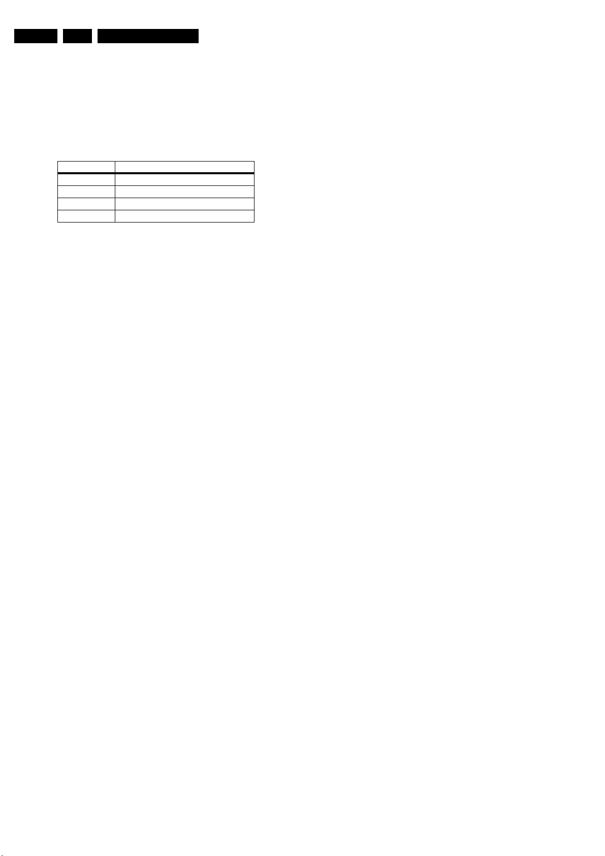
EN 76 DPTV4658.
Alignments
1. During the IF AFC-parameter adjustment, one can see
OSD feedback on the screen.
2. The OSD feedback can give 4 kinds of messages:
3. The first item (IN/OUT) informs you whether you are in or
out of the AFC-window.
4. The second item (HIGH/LOW) informs you whether the
AFC-frequency is too high or too low.
Table 8-2 OSD feedback of AFC alignment
AFC-window AFC-frequency vs. reference
Out High
In High
In Low
Out Low
1. Adjust the IF AFC parameter until the first value is within
the AFC window (= IN).
2. Next, adjust the IF AFC parameter until the second value
is LOW.
IF LPRIME AFC
Same procedure as described above but with other signal
source (SECAM L').
TUNER AGC
1. Connect the RF output of a video pattern generator to the
antenna input.
2. From the generator, input a PAL B/G TV signal with a
signal strength of approximately 2 mV and a frequency of
475.25 MHz (PAL) or 61.25 MHz (NTSC).
3. Measure the DC voltage on pin 1 of the (main) Tuner. You
can adjust this voltage by adjusting the TUNER AGC item
in the SAM menu. Alignment is correct when the DC
voltage is just below 3.5 V.
IF AFC TUNER 2 (if present)
Use the same procedure as described above (under IF AFC)
with the set switched to the DW source.
IF LPRIME AFC TUNER 2 (if present)
Use the same procedure as described above (under IF
LPRIME AFC) with the set switched to the DW source.
TUNER AGC TUNER 2
Use the same procedure as described above (under TUNER
AGC) with the set switched to the DW source. Measure on pin
“1” of the DW Tuner.
BLEND INTENSITY
Use this alignment when you replace the microcontroller or the
HOP. It aligns the level of transparency of the menu-picture
blended into the main-picture.
Position the "Brightness", "Contrast", and "Colour" setting in
the middle position (in the customer "Picture" menu).
1. Apply a signal with a 100 % white video pattern (white
raster).
2. Connect an oscilloscope to pin 8 of connector 1298 of the
CRT panel and measure the Red output level.
3. Align the BLEND INTENSITY parameter so that the
blended signal is 65 % of the black-white amplitude. This
will be about 1.3 V (blended signal) versus 2 V (full white
signal).
4. The parameter can be adjusted from 0 to 31.
8.3.2 LUM. DEL. (Luminance Delay)
With this alignment, you place the luminance information
exactly on the chrominance information (brightness is pushed
onto the colour). Use a colour bar / grey scale pattern as test
signal.
• LUM. DELAY PAL BG: Apply a PAL BG colour bar / grey
scale pattern as a test signal. Adjust this parameter until
the transients of the colour part and black and white part of
the test pattern are at the same position. Default value is
"9".
• LUM. DELAY PAL I: Apply a PAL I colour bar/grey scale
pattern as a test signal. Adjust this parameter until the
transients of the colour part and black and white part of the
test pattern are at the same position. Default value is "9".
• LUM. DELAY SECAM: Apply a SECAM colour bar/grey
scale pattern as a test signal. Adjust this parameter until
the transients of the colour part and black and white part of
the test pattern are at the same position. Default value is
"11".
• LUM. DELAY BYPASS: apply a NTSC colour bar/
greyscale pattern as a test signal. Adjust this value until the
transients of the colour and black and white part of the test
area are at the same position. Default value is "10".
8.3.3 GDE SAM
Specifications:
• Set display mode in service mode.
• Service blanking.
• Set geometry.
• Preset picture.
• Set white tone.
• Convergence disable for setting geometry.
The GDE SAM mode (GDE = Generic Display Engine), allows
the Service Technician to set Geometry and White Tone (Grey
Scale). This mode is controlled by the GDE microprocessor
located on the ASC module. These settings are stored in an
EEPROM located on the ASC module. The GDE SAM displays
the Software version of the GDE microprocessor and the GDE
Errors.
There are three settings for Geometry in the 4x3 aspect ratio
sets and two for the 16x9 aspect ratio sets.
The signal for the 480p mode can be applied to the set via the
HD YPbPr inputs or from the SSB when the set is in the NTSC
mode. All Geometry alignments for this mode should be done
with an NTSC signal selected.
Adjustments for the 1080i should be done with an HD 1080i
signal applied to the set. The 4x3 aspect ratio sets have both a
Full and Compressed mode that requires alignment.
The Service Blanking selection (SERV BLANK) will blank the
bottom half of the picture. This selection is useful when
adjusting the Yokes to level the picture.
The Clamp Pulse should be set to Normal for a 480p or NTSC
signal. It should be set to 1080i for an HD signal.
The Convergence Processor selection will enable or disable
Convergence drive. Convergence should be disabled when
performing Cantering or Geometry alignments.
8.4 Convergence and Geometry Adjustments
8.4.1 Introduction
If the ACS module has been replaced, the following
adjustments will be required in the order as shown:
1. Geometry.
2. Convergence.
3. Grey Scale (White Tone).
If the Large Signal Board (LSB) has been changed the
following adjustment are required:
1. Geometry.
2. Convergence.
If one or more CRTs have been replaced:
1. Geometry.
2. Convergence.
Page 77
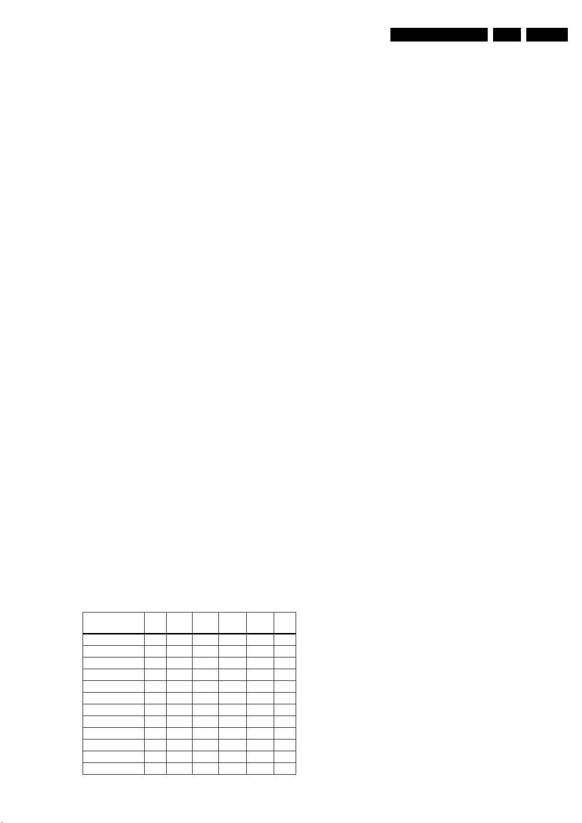
Alignments
EN 77DPTV465 8.
3. Grey Scale (White Tone).
If the SSM (Small Signal Module has been changed:
1. Convergence.
Enter the Service Alignment Mode (SAM) by pressing the
following key sequence on the remote control transmitter: 0-6-
2-5-9-6-[i+]. Do not allow the display to time out while entering
the key sequence.
Cursor down to the Alignments level and then Cursor right to
locate the GDE SAM. Press the OK button to enter the GDE
SAM mode.
Note: Read the complete following text before starting the
alignments.
8.4.2 Screen Centring
If one or more CRTs are replaced, it will be necessary to
perform Screen Centring.
1. Place the Convergence Template on the TV screen or
place a string from corner to corner to determine the screen
centre.
2. Apply a centre cross pattern to the TV.
3. Enter the SAM mode, described in the Geometry section
and disable Convergence.
4. Cover the Red and Blue CRTs.
5. Using the Centring rings on the Green CRT, centre the
cross onto the centre of the template.
6. Uncover the Red CRT and centre the Red onto the Green
cross.
7. Follow the same procedure with the Blue CRT.
Note: Only perform the Screen Centring for the first mode to be
adjusted. Do not repeat the adjustment for the other modes.
8.4.3 Geometry Alignment
The Geometry alignment data is stored in the NVM, located on
the ACS module. Whenever the ACS module or the Large
Signal Board (LSB) have been changed, a Geometry alignment
will be necessary. The Geometry Alignment is performed in the
GDE SAM alignment mode. Make sure the set is in the mode
in which you wish to align before entering the SAM mode. Use
the AV button on the Remote to select the input with a signal,
applied after entering the SAM mode.
Apply a crosshatch pattern to the set. Cursor Down to CONV
PROC in the menu and press the Right Cursor button to select.
This will disable the Convergence drive. Select GEOMETRY in
the menu and enter the following default values for the mode
being adjusted.
After entering the default values, the E-W WIDTH, VERTICAL
SLOPE, and VERTICAL AMP should be the only settings
requiring further adjustment.
Note: Perform (and store) Convergence alignment after any
changes to the Geometry.
8.4.4 Convergence Mode
There are two new screen sizes for the AP region incorporating
a Digital Convergence system using 208 adjustment points.
The Convergence Processor is located on the ACS (Automatic
Convergence System) module. The Convergence drive circuits
are located on the SSP (Small Signal Panel). Data for the
Convergence and Geometry settings are stored in the
EEPROM located on the ACS module.
If the CRTs, the Large Signal Panel (LSP), or the Small Signal
Module (SSM) are changed, a complete Geometry and
Convergence alignment will be necessary.
If the ACS module, the Small Signal Panel (SSP), or CRTs are
changed, a complete Convergence alignment will be
necessary.
To obtain the correct Geometry during Convergence, a
template must be used. There are eight Geometry and
Convergence settings, stored in the EEPROM on the ACS
Module.
• 43 inch 4x3 aspect ratio - Use Template ST4177
• 50 inch 4x3 aspect ratio - Use Template ST4178
• 55 inch 16x9 aspect ratio - Use Template ST4181
8.4.5 Convergence Alignment
Enter the Service Alignment Mode (SAM) by pressing the
following key sequence on the remote control transmitter:
0-6-2-5-9-6-[i+]. Do not allow the display to time out while
entering the key sequence.
Make sure that a signal is applied to the set for the mode being
adjusted.
Make sure that the set is in the mode you wish to adjust before
entering the Convergence Alignment mode.
Table 8-3 Geometry Default Values
480p 1080i 1080i
Wide blank 7 7 7 7 7 7
Horizontal Shift 24 21 21 25 24 26
Horizontal Para 8 8 8 8 8 8
E-W Width 31 44 44 31 31 31
E-W Para 45 45 45 45 45 45
E-W Trap 31 31 31 31 31 31
Horizontal Bow 7 7 7 7 7 7
Vertical Slope 40 33 33 37 38 38
Vertical Ampl 40 40 12 41 44 39
S Correction 31 31 31 31 31 31
Vertical Shift 31 31 31 31 31 31
Fast Blank 0 1 0 0 0 0
100Hz 120Hz 576p
Comp
Page 78
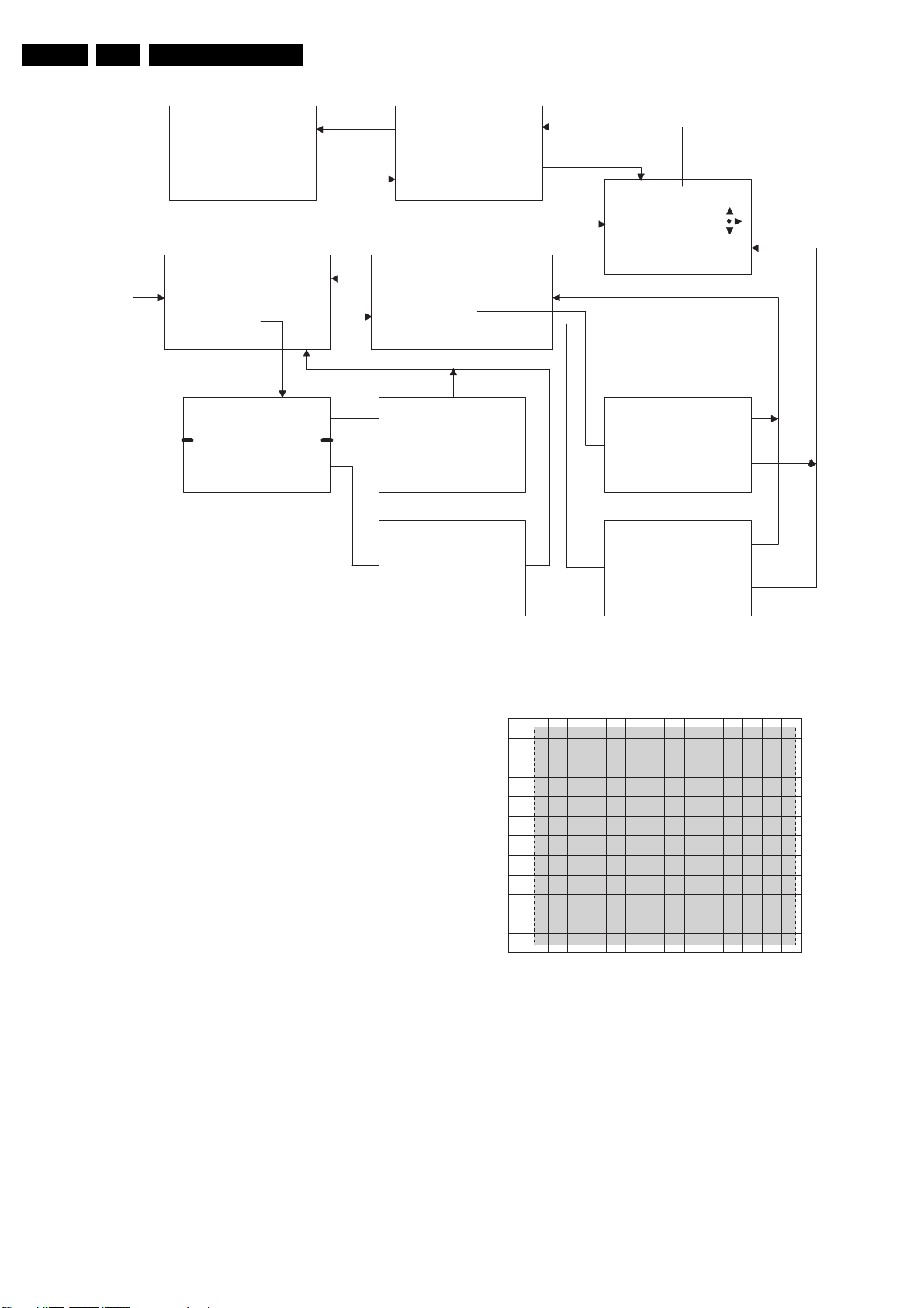
EN 78 DPTV4658.
Alignments
0 6 2 5 9 7 I+
USE CURSOR KEYS TO HIGHLIGHT
USE MENU KEY TO SELECT
USE STATUS KEY TO RETURN
CURSOR KEYS TO ADJUST
MENU TO CHANGE
STEP SIZE
I+ TO RETURN
CURSOR RIGHT TO SELECT
POWER OFF TO EXIT CONVERGENCE
CONVERGENCE ADJUSTMENTS
SENSOR TEST
1
2
4
MENU
I+
I+
3
CURSOR KEYS TO
NAVIGATE
MENU TO ADJUST
I+ TO RETURN
MANUAL CONVERGENCE WO VIDEO
MANUAL CONVERGENCE W VIDEO
RESTORE FACTORY
RESTORE DEFAULTS
CURSOR RIGHT TO SELECT
I+ TO RETURN
SENSORS NOT VERIFIED
AT LOCATIONS______
MENU TO TEST AGAIN
I+ TO RETURN
SENSORS OK
I+ TO RETURN
CURSOR RIGHT
I+
GREEN
RED TO GREEN
BLUE TO GREEN
GREEN TO RED
BLUE TO RED
SP RED
SP BLUE
MP RED
MP BLUE
STORE
I+
MENU TO SAVE DATA
I+ TO RETURN
MENU TO SAVE DATA
I+ TO RETURN
MENU
Figure 8-1 Convergence menus
Use the Cursor Up-Down button to highlight the selection.
Press the Cursor Right button to make the selection. In the
second menu:
• MANUAL CONVERGENCE WO VIDEO means that the
screen behind the adjustment grid will be blank. This does
not mean that Convergence can be performed without a
signal being applied to the set.
• MANUAL CONVERGENCE W VIDEO displays the applied
video behind the adjustment grid.
• RESTORE FACTORY loads the values from the last saved
convergence alignment.
• RESTORE DEFAULT loads values from the ROM on the
ACS Microprocessor.
• RESTORE FACTORY or RESTORE DEFAULT will
overwrite all eight Convergence modes.
If the ACS module has been changed, there may not be data in
the NVM for RESTORE FACTORY. The RESTORE DEFAULT
settings will then be loaded.
An internally generated grid will be displayed in the
Convergence mode as shown on the following page. The
shaded area is the visible screen area. Horizontal lines A and
M are displayed on the top and bottom edge of the visible
screen area. Lines 1 and 15 are also displayed on the left and
right edge of the visible screen area. Vertical line 0 is adjustable
but not visible.
0
123456789101112131415
A
B
C
D
E
F
G
H
I
J
K
L
M
Figure 8-2 Convergence alignment grid
8.4.6 Single Tube Replacement Convergence
If a single tube has been replaced, it is not necessary to do a
Major Convergence alignment.
1. Enter the Convergence mode and select the adjustment
needed.
2. Select "Red to Green", for example if the Red tube has
been replaced.
3. Adjust the centring rings on the CRT to centre the Red
pattern onto the Green pattern.
4. Starting with the centreline, adjust the Red icon onto the
Green pattern. Best results are obtained when navigating
from left to right. Two or three passes may be necessary to
obtain satisfactory results.
E_15000_062.eps
E_15000_063.eps
151004
151004
Page 79
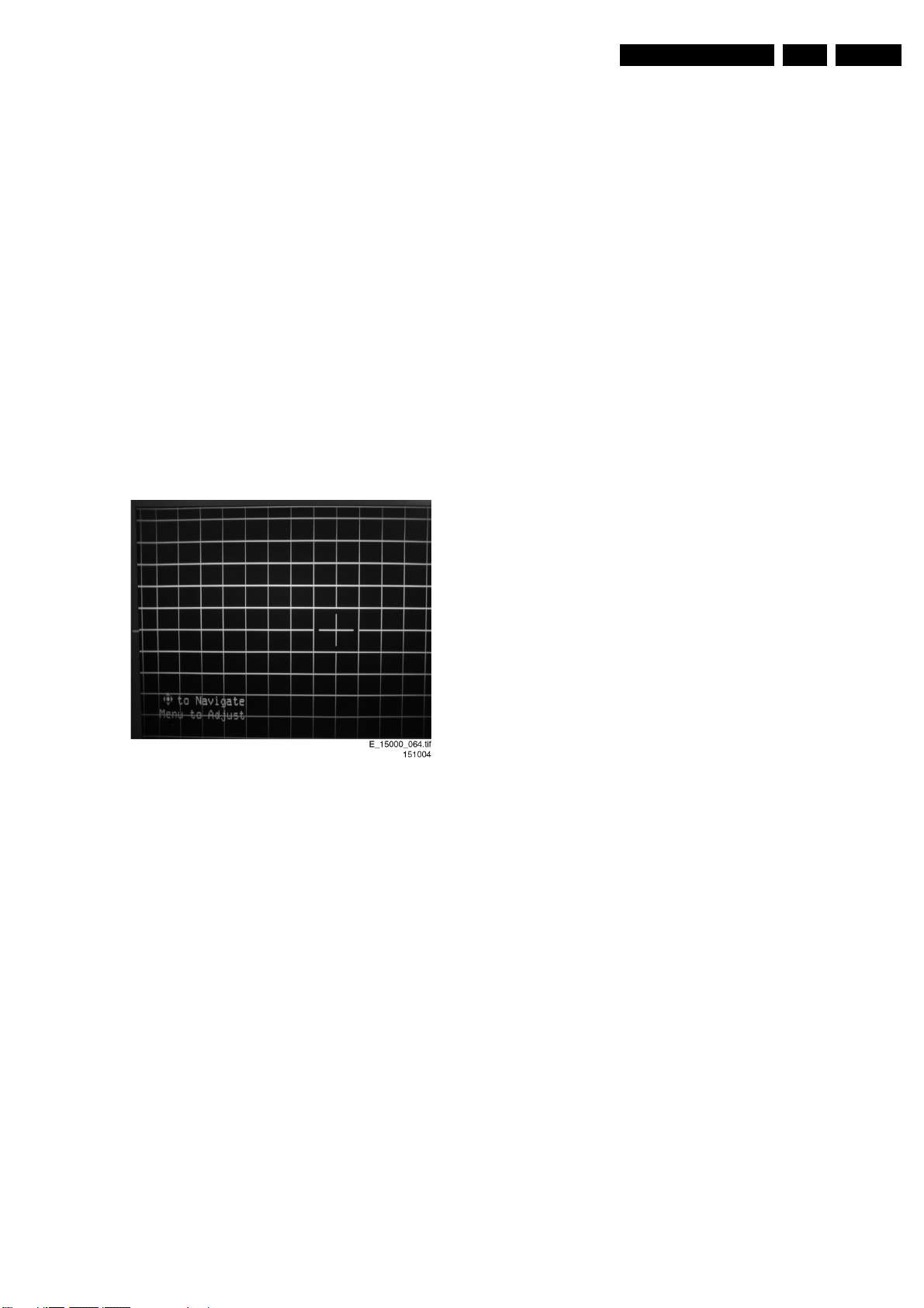
Alignments
EN 79DPTV465 8.
8.4.7 Touch Up Convergence
When making minor Convergence corrections, move the
Cursor to the location to be adjusted then press the MENU
button to adjust that location. When in the adjustment mode,
press the MENU button a second time if it is desired to change
the step size of the adjustment. When making minor
Convergence corrections, you may adjust the following:
• RED TO GREEN
• BLUE TO GREEN
• SP RED
•MP RED
• SP BLUE
• MP BLUE
8.4.8 Green Geometry
Important: Do not make changes to the Green Geometry
without placing a Template over the screen.
The Green Geometry must be done first when performing a
complete convergence alignment. A Screen Template is
necessary to obtain the correct geometry. Failure to use the
Screen Template or mis-adjustment of the convergence will
result in reduced life of the Convergence amplifiers.
Figure 8-3 Screen shot of "Green geometry" adjustment
Place the Screen template on the TV screen. Select GREEN in
the selection menu. The Cursor will appear in the centre of the
screen as shown in the picture.
When the ACS module has been replaced, it would be
advisable to load Default settings. Press the MENU button to
adjust, and then use the Cursor buttons to move the Green
cross onto the Template.
The adjustment of the cross has two-step sizes: large and
small. Press the MENU button to toggle between the two.
After a point has been adjusted, press the Index button to
return to Navigate. When Default settings have been loaded,
the left most line that is not visible should be adjusted first.
Adjust the Vertical line 0 while observing line 1 to make line 1
parallel with the left edge of the screen. The adjustment should
only be made in small steps.
Do not adjust any one point more than 1/4 the distance of one
grid in each pass. After the left most line is adjusted, start at the
centre left of the screen and work to the right, aligning the
Horizontal lines. When adjusting the Horizontal lines, best
results are obtained when working from left to right.
After the Centre line is adjusted, go to the next line down until
all of the lines have been adjusted, then work from the centre
up to adjust the Horizontal lines. Using the same method, work
from centre out to adjust the Vertical lines. At least three
passes will be necessary to complete the alignment. Press the
Index button to return to the selection menu.
When the GREEN geometry is complete, STORE the data.
Remove the template from the screen. Select RED TO GREEN
in the selection menu. Using the same method that was used
to adjust the Green Grid to the Template, adjust the Red Grid
onto the Green Grid. If the set is a later production, select SP
RED to centre the Red grid onto the Green grid. Exit this mode
by pressing the MENU button. Then select the MP RED to
adjust the Red onto the Green using the 35-point adjustment.
When this is complete, select the RED TO GREEN to perform
the 208-point adjustment.
When the RED TO GREEN is complete, select the BLUE TO
GREEN, using the same alignment method as the RED TO
GREEN.
Select STORE to save your the alignments after adjusting each
colour. Each time data is stored; the Intellisense circuit will
recalculate the position of the four sensors in the set.
Exiting the Convergence Mode without saving will cause the
alignments to be lost.
Repeat the adjustment for each of the remaining modes.
8.4.9 Grey Scale Alignment
1. Place the input to the RGB (AUX 5) or YPbPr (AUX 4)
mode. Connect a Computer or Computer monitor
generator to the AUX 5 input or a Component Generator to
AUX 4.
2. Preset the G2 controls counter clockwise.
3. Turn the Green G2 clockwise to make the menu visible.
4. Enter the SAM mode by entering 0-6-2-5-9-6-[i+] on the
Remote Control. Select the GDE mode and select WHITE
TONE.
5. Preset the following registers: Use the Cursor Right-Left
buttons to set the value. Use the Cursor Up-Down buttons
to select the register. Press the MENU button to exit the
WHITE TONE menu.
– NORMAL RED CUT-OFF: “32”
– NORMAL GREEN CUT-OFF: “25”
– NORMAL BLUE CUT-OFF:”31”
– NORMAL RED DRIVE: “22”
– NORMAL GREEN DRIVE: “58”
– NORMAL BLUE DRIVE: “40”
6. Set the BRIGHTNESS, PICTURE, and SHARPNESS to
their midpoint position. Select a Black Raster pattern on the
computer or computer monitor generator.
7. Connect an Oscilloscope, set to measure DC, to each
cathode to determine the dominant (lowest) colour.
8. Adjust the SUB BRIGHTNESS control to set the Black
Level equal to 180 Volts on the Oscilloscope.
9. Move the probe to the remaining cathodes and adjust the
corresponding cut-off registers to make the black part of
the waveform at 180 Volts.
10. Set the corresponding G2 control to just make cut-off for
the black part of the waveform for that tube.
11. Remove the Oscilloscope probe.
12. Apply a Greyscale pattern to the set.
13. Adjust the Drive Controls to achieve the proper white
balance. At least one drive should remain 3F.
14. The following Drives and Cut-offs should be set as listed.
These are in the WHITE TONE menu.
– COOL CUT-OFF RED: “0”
– COOL CUT-OFF GREEN: “0”
– COOL CUT-OFF BLUE: “0”
– COOL DRIVE RED: “-7”
– COOL DRIVE GREEN: “-6”
– COOL DRIVE BLUE: “0”
– WARM CUT-OFF RED: “0”
– WARM CUT-OFF GREEN: “0”
– WARM CUT-OFF BLUE: “0”
– WARM DRIVE RED: “+7”
– WARM DRIVE GREEN: “+4”
Page 80
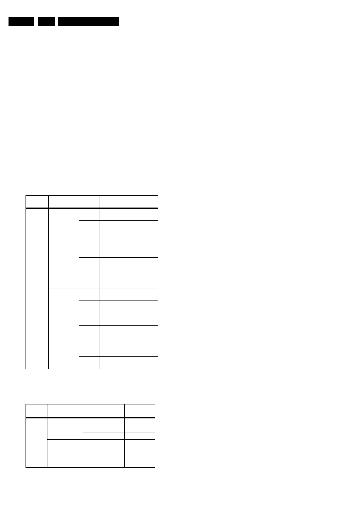
EN 80 DPTV4658.
Alignments
– WARM DRIVE BLUE: “-6”
15.Press the MENU button to return to the SAM menu. Exit the
Service mode by turning the set ”off”.
8.5 Option Settings
8.5.1 Introduction
The microprocessor communicates with a large number of I2C
ICs in the set. To ensure good communication and to make
digital diagnosis possible, the microprocessor has to know
which ICs to address. The presence / absence of these specific
ICs (or functions) is made known by the option codes.
Notes:
• After changing the option(s), save them with the STORE
command.
• The new option setting is only active after the TV is
switched "off" and "on" again with the Mains switch (the
EAROM is then read again).
8.5.2 DEALER OPTIONS
Table 8-4 Dealer options
Menu
name Subjects
Personal
Options
Picture Mute Yes Picture mute active in
Virgin Mode Yes TV starts up once with
Auto Store
Mode
TXT
Preference
Option
s Physically in set
case no picture detected
No Noise in case of no picture
detected
language selection menu
after mains switch on for
the first time (virgin mode)
No TV does not starts up
once with language
selection menu after
mains switch on for the
first time (virgin mode)
None Autostore mode disabled
(not in installation menu)
PDCVPS
TXT
page
PDCVPSTXT
TOP Preference to TOP
FLOF Preference to FLOF
Autostore mode via ATS
(PDC/VPS) enabled
Autostore mode via ACI
enabled
Autostore mode via ACI or
ATS enabled
Teletext
Teletext
8.5.4 Option Codes
Enter the Service Alignment Mode (SAM) by pressing the
following key sequence on the remote control transmitter:
0-6-2-5-9-6-[i+]. Do not allow the display to time out while
entering the key sequence.
Cursor to the OPT. NO. in the SERVICE OPTIONS level.
Locate the “option code label” on the inside right panel of the
unit and enter the correct codes for the model being serviced.
Example
• Group 1: 49483 32801 33055 32793
• Group 2: 39897 32768 32768 00000
Note: Remember to cursor to the STORE OPTIONS level and
select “OK” to save these changes
8.5.3 SERVICE OPTIONS
Table 8-5 Service options
Menu
name Dual screen
Service
Options
Video repro Lightsensor Yes/No
Miscellaneous Tuner Type TEDE9/
Opt. No. Group 1
TXT/EPG Dual
Screen Yes/No
2D Combfilter Yes/No
Pixel Plus Yes/No
UV1316
Group 2
Page 81
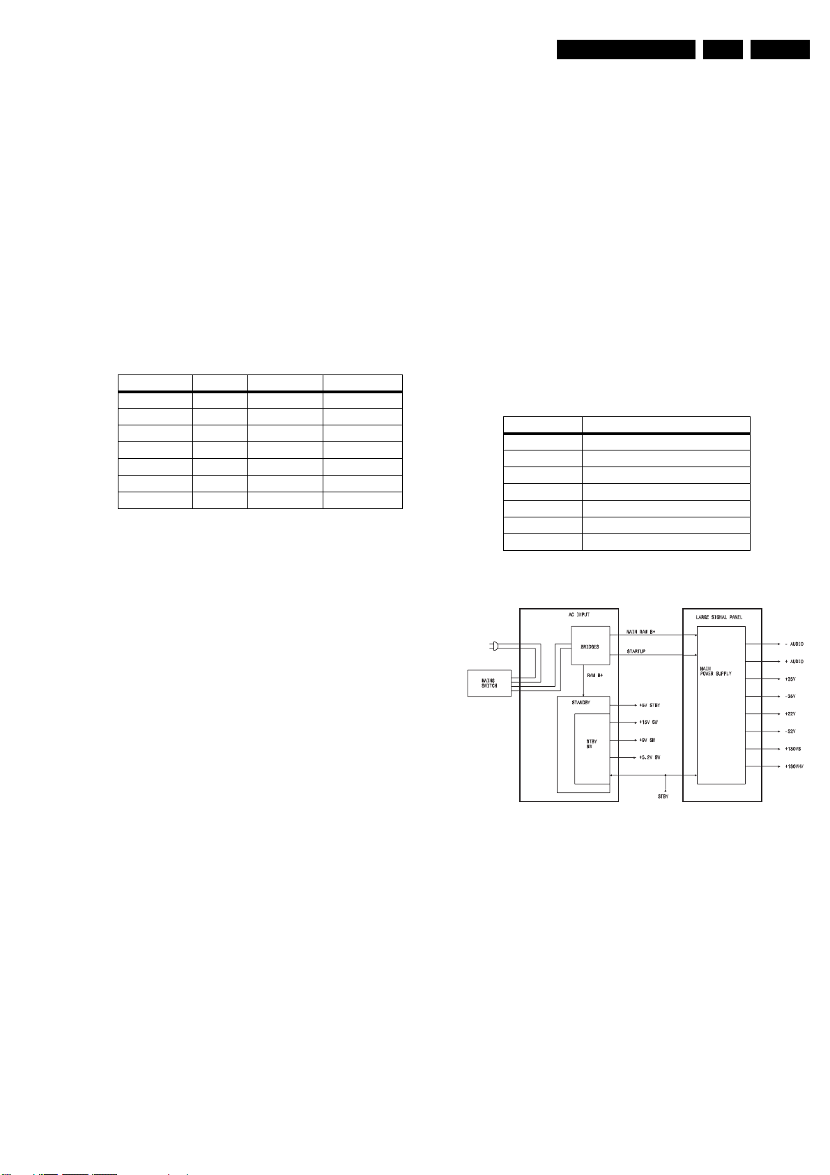
Circuit Descriptions, List of Abbreviations, and IC Data Sheets
EN 81DPTV465 9.
9. Circuit Descriptions, List of Abbreviations, and IC Data Sheets
Index of this chapter:
9.1 Introduction
9.2 Power Supplies
9.3 Video
9.4 Audio
9.5 Control/OSD
9.6 List of Abbreviations
9.7 IC Data Sheets
9.1 Introduction
Two new chassis are being introduced for the Asia Pacific
region in the 2003/2004 model year. The table below lists the
Model and Chassis numbers.
Table 9-1 Model and chassis overview
Model Chassis Aspect Ratio Destination
43PP8445/93 DPTV465 4x3 China
43PP8446/93 DPTV465 4x3 China
43PP8447/93 DPTV465 4x3 China
43PP8545/69 DPTV465 4x3 Singapore
50PP8545/69 DPTV465 4x3 Singapore
50PP8545/93 DPTV465 4x3 China
55PP8745/93 DPTV465 16x9 China
All the chassis have multi-system tuning capability. The set has
the capability of displaying the 1080i, 1152i, 480p, and 576p
high definition component analogue inputs. The 1fH RF inputs
can be PAL or SECAM. The 1fH AV inputs can be YPbPrcomponent, composite, or SVHS.
Some of the highlights are:
• TV-off air systems (PAL and SECAM).
• Korean sets NTSC only.
• NTSC (3.58 - 4.5 MHz).
• NTSC (4.43 - 5.5 MHz).
• PAL B/G, PAL D/K, PAL I, PAL M, PAL N.
• SECAM B/G, SECAM D/K, SECAM K1.
• HD signal inputs are analogue.
• Component in.
The sets have 1fH multi-system composite, SVHS, and
component inputs. The External 1fH or TV RF signals are fed
to the Picnic and Eagle circuits, where the user can select
between 100 Hz Digital Scan or Double lines.
External input systems:
• NTSC 3.58 MHz
• NTSC 4.43 MHz
• PAL
• SECAM
• 480p, 576p, 1080i, 1152i component input
• 480p, 1080i Korean set
All of the sets, based on the PEMG, have a 4x3 aspect ratio,
except the 55” version which has a 16x9 aspect ratio. There are
eight different scan modes with each requiring separate
geometry and convergence settings. The modes are PAL
100Hz, PAL 75 Hz, 576p, 576p DVD, 480p, 480p DVD, 1080i,
and 1152i. Each of the modes has separate geometry and
convergence data, stored in the NVM, located on the ACS
(Automatic Convergence System) module.
Sound System processing is performed on the SSB (Small
Signal Board). This is a multi-system sound decoding
processor. The audio amplifier is located on the SSM (Small
Signal Module). This is a 30 Watt (2 x 15 Watts) digital
amplifier. There is also a Headphone output, located on the
Side Jack Panel. The headphone amplifier is located on the
SSM.
Sound system:
• 30 W (2x15W) Audio.
• Headphone Out.
• Speaker "on"/Off.
9.2 Power Supplies
The Rectifiers and Standby Supplies are located on the AC
Input Panel. The Main Power Supply is located on the Large
Signal Board (LSB).
In the table below, the models are listed with their respective
voltage requirements. Auto Multi Voltage sets have a voltage
range of 90 to 276 V.
Table 9-2 Voltage range overview
Model Voltage Range
43PP8445/93 160 - 276V nominal 230 V
43PP8446/93 160 - 276V nominal 230 V
43PP8447/93 160 - 276V nominal 230 V
43PP8545/69 Auto Multi-Voltage
50PP8545/69 Auto Multi-Voltage
50PP8545/93 160 - 276V nominal 230 V
55PP8745/93 160 - 276V nominal 230 V
9.2.1 Overall Power Supply Block
Figure 9-1 Power supply block diagram
The bridge rectifiers and Standby supply are located on the AC
Input Panel. The Main Power supply is located on the Large
Signal panel. A mains switch switches the AC power to the
bridge rectifier, located on the AC Input panel. This switch must
be turned "on", to place the set in the Standby mode. The
Standby supply produces a +5 Volt standby voltage. In the
Standby mode, the set consumes less than 1 W of power.
When the set is turned "on", the microprocessor on the SSB
causes the STANDBY line to go "low", switching the Standby
supply to produce +15 V, +9 V, and +5.2 V sources. It also turns
the Main Power supply "on", which produces the Audio, +35, 35, +22, -22, +130 V_S, and +130 V_HV supplies. The +130
V_S supply is for the Horizontal Output section. The +130
V_HV supplies power to the High Voltage section.
E_15000_066.eps
151004
Page 82
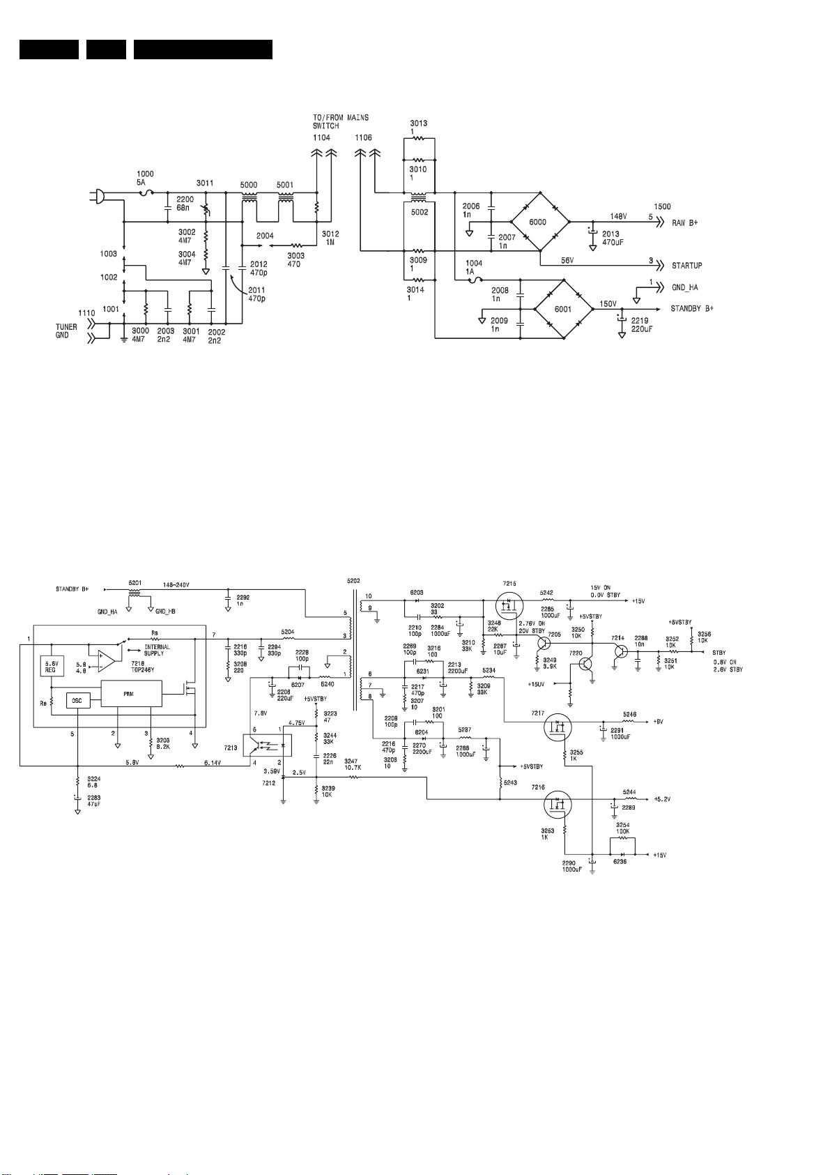
EN 82 DPTV4659.
9.2.2 AC Input Board
Circuit Descriptions, List of Abbreviations, and IC Data Sheets
The AC power is fed to the AC Input panel. A 5 A fuse (item
1000), provides protection. Chokes 5000 and 5001 provide
filtering for the AC. The Mains switch is connected via
connectors 1104 and 1106. Resistors 1003, 1002, 1001, and
3011 provide protection against Line Surges in the non-China
sets. In the China sets, resistors 3009, 3014, 3013, and 3010
have been replaced with choke 5002 to provide additional AC
filtering.
9.2.3 Standby Power Supply
Figure 9-2 AC input board
E_15000_067.eps
Bridge 6001 rectifies the voltage for the Standby Power supply.
Resistors 3009, 3014, 3013, and 3010 provide current limiting
when power is first applied to the set. Bridge 6000 rectifies the
voltage for the Main power supply. Start-up voltage for the Main
Power supply is taken from the neutral side of the AC line. Fuse
1004 provides protection for the Standby Power supply.
151004
Figure 9-3 Standby power supply circuit
The Standby Supply provides the 5V_STANDBY voltage to the
set in the Standby mode. When the set is turned "on", it
provides the +15, +9, and +5.2 Volts supplies.
Standby B+ is applied to the Standby Switching regulator 7218
via pins 5 and 3 of 5202. An internal switch in 7218 charges
capacitor 2283 connected to pin 1 of the IC. When the charge
on 2283 reaches 5.8 Volts, the internal switch switches to
internal. The IC is now being powered by the charge on
capacitor 2283. The internal FET drives transformer 5202 until
the charge on capacitor 2283 reaches 4.8 Volts. The IC repeats
the cycle until the 5 Volt Standby voltage reaches the correct
E_15000_068.eps
151004
level. Shunt regulator 7212 then turns "on", turning opto
isolator 7213 "on". The operating voltage for 7218 is then
supplied by the rectified hot secondary voltage from pin 1 of
5202. The internal regulator keeps pin 1 at 5.8 Volts.
Regulation is accomplished by monitoring the 5 Volt standby
voltage. If the 5 Volt supply increases, shunt regulator 7212 will
conduct more, causing the resistance of the transistor inside
7218 to decrease. The sensing resistor, Re, inside 7218 will
sense the increase in current and reduce the "on" time of the
internal FET, which will lower the 5 Volt supply to the correct
level.
Page 83
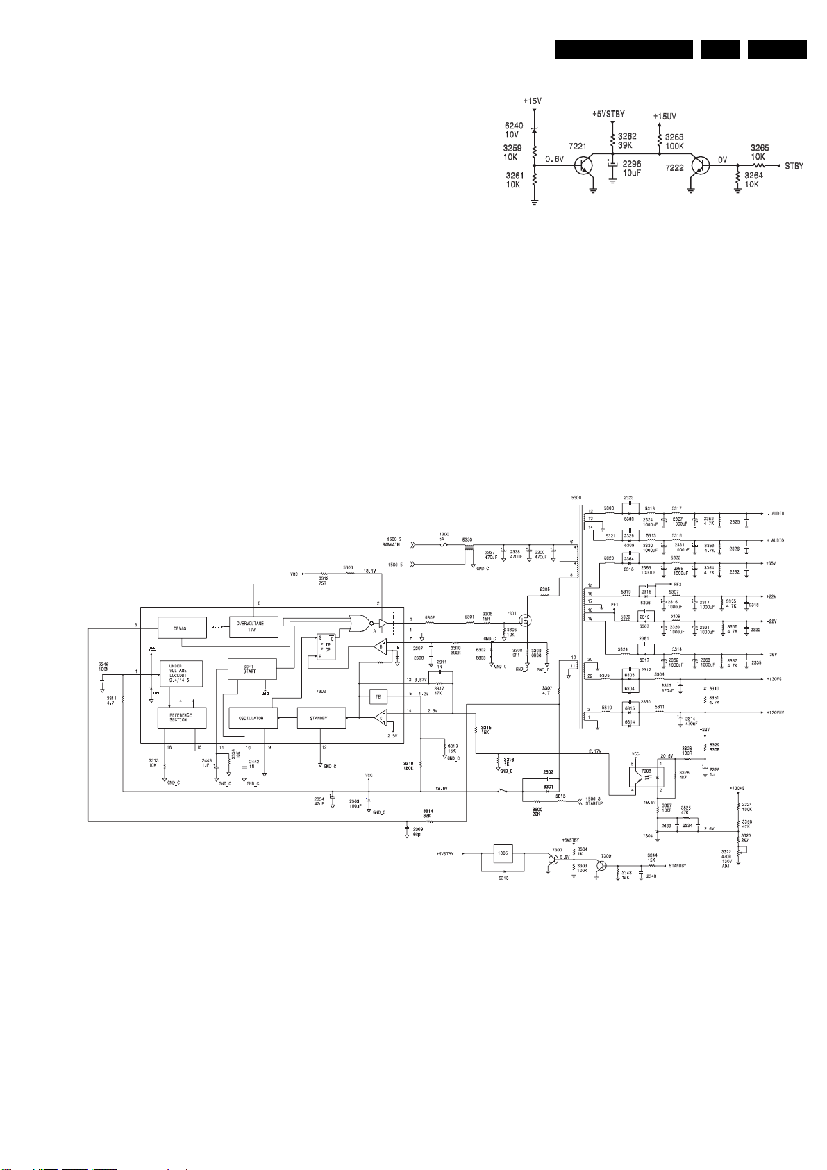
Circuit Descriptions, List of Abbreviations, and IC Data Sheets
EN 83DPTV465 9.
In Standby, the-5 volt Standby voltage is the only voltage being
applied to the set. The +15, +9, and +5.2 Volt sources are
turned "off". When the set is turned "on", the Standby Line goes
Low, turning transistor 7214 "off", turning 7205 "on", which
turns 7215 "on". This switches the +15 Volt supply to the set.
The +15 Volt supply then switches transistors 7216 and 7217
"on" to switch the +9 Volt and +5.2 Volt supplies to the set.
When the +15UV (Under Voltage detection) line goes "high",
transistor 7220 will turn "on", which will turn 7205 "off". This will
cause 7215 to turn "off", switching the +15, the +9, and the +5.2
Volt supplies "off". This will cause the set to shut down.
When troubleshooting, check for the presence of the operating
voltage on pin 7 of 7218. This 160 volts if the applied voltage is
120 volts AC or 328 volts is then applied voltage is 230 Volts
AC. If the Feedback circuit is not working or the secondary is
overloaded, pin 7 will be pulsing. In this case, check the voltage
on pin 5 of 7213. This is the operating voltage for pin 1 of 7218.
Each time the 5VSTBY voltage reaches 5 Volts, 7212 should
turn "on". The feedback opto isolator 7213 can be checked by
applying 5 volts to the +5VSTBY line with AC power removed
from the set. Vary the 5- volt supply between 4 and 6 Volts
while checking the resistance between Pins 4 and 5 of 7213.
9.2.4 Main Power Supply
Under voltage Detection
E_15000_069.eps
151004
Figure 9-4 Under voltage detection circuit
If the 15-Volt supply drops below 11.2 Volts, transistor 7221 will
turn "off". The 5-Volt standby supply will be applied to the base
of 7220 (Figure " Standby power supply circuit") via resistors
3262 and 3263. This will cause the +15UV line to go "high". In
the Standby mode, the Standby line is "high" turning transistor
7222 "on". When the set is turned "on", 7222 turns "off".
Capacitor 2296 provides a delay to prevent the +15UV line
from going "high" before the +15V supply turns "on".
This circuit can be defeated by grounding the base of transistor
7220. When repairs are complete, this jumper should be
removed.
Figure 9-5 Main power supply circuit
The Main Power supply is located on the Large Signal panel.
The Main B+ voltage from the Input panel is applied to the Main
Power switching transistor, 7301, via Pins 6 and 8 of
transformer 5300. This voltage is protected by fuse 1300 and
filtered by choke 5330. The Standby line goes "low" when the
set is turned "on". Transistor 7309 is turned "off", which turns
7300 "on". This turns relay 1305 "on". The Start-up voltage is
applied to capacitor 2303 via resistor 3300. When 2303
charges to 14.5 Volts, the under-voltage lockout of 7302
connected to pin 1 is turned "on". Drive is output on pin 3 to the
switching FET, 7301. This signal drives 5300 to produce the
Main Power supply voltages. IC 7302 will continue to drive
E_15000_070.eps
151004
5300 until the charges on capacitor 2303 drop below 9.4 Volts.
The Under voltage Lockout of 7302 will then turn the output on
pin 3 "off" until 2303 again charges to 14.5 Volts. After several
start-up cycles, the operating voltage for 7302 is supplied by
pin 10 of 5300.
Regulation is accomplished by monitoring the 130V_S supply
via resistors 3324, 3350, 3323, and 3322. The feedback
voltage is applied to the Shunt Regulator 7304, which drives
the feedback opto-isolator 7303. The feedback voltage is
applied to pin 14 of 7302. The voltage is fed to comparator "C"
which is referenced to 2.5 Volts. This output of this comparator
Page 84
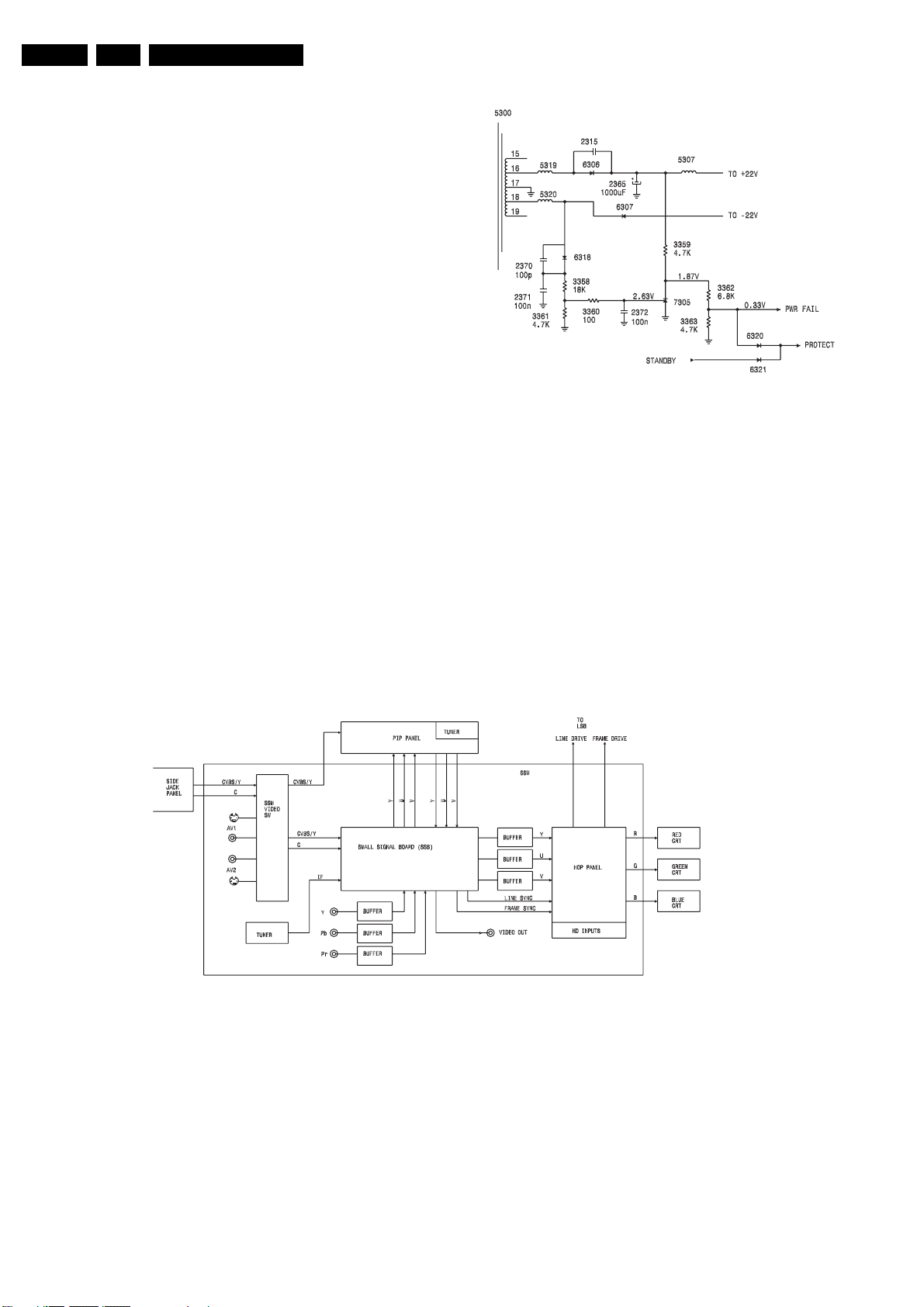
EN 84 DPTV4659.
Circuit Descriptions, List of Abbreviations, and IC Data Sheets
sets the reference voltage for comparator "B", which is
compared with the voltage on the source of 7301. This voltage
is developed when 7301 turns "on", causing current to flow
through resistors 3308 and 3309. If 7301 fails, Resistors 3308
and 3309 should be replaced. These are one percent tolerance
resistors.
The Main Power supply produces: +130 V, +35 V, +22 V, -22
V, -35 Volt, a plus audio supply, and a minus audio supply. The
Audio supply is a plus and minus 23 Volts. This supplies the
digital audio amplifier located on the SSM (Small Signal
Module).
When troubleshooting, notice that the Hot Ground for the Main
Power supply is separated from the main Hot Ground on the
AC Input Panel by Choke 5330. To ensure correct readings,
use the Hot Ground in the Main power supply. If the power
supply is overloaded or the operating voltage is missing, the
voltage on pin 1 of the IC should be changing between 9.4 and
14.5 Volts. Each time the voltage reaches 14.5 Volts, drive
should appear on pin 3 of the IC. If a voltage is present on pin
1 that is greater than 14.5 Volts and there is no drive on pin 3,
the IC should be replaced. If drive is present on pin 3, check for
drive on the Drain of 7301. If drive is present here, check for a
short on the 130 Volt lines, a problem in the feedback circuit, or
a problem with the operating voltage.
Power Fail Shutdown
E_15000_071.eps
151004
Figure 9-6 Power fail shutdown circuit
The +22 Volt supply is rectified by 6306 and the -22 Volt supply
is rectified by 6307. The voltage on pin 18 of 5300 is monitored
to detect a failure of the AC supply to the set. This circuit
signals the microprocessor in the event that AC is removed
from the set while it is turned "on". The voltage from pin 18 is
rectified by 6318 and is applied to the Shunt Regulator 7305.
Shunt Regulator 7305 is turned "on", keeping the Power Fail
and Protect lines Low. When AC is removed while the set is
"on", 7305 will turn "off" fast. This is because the filter capacitor
for the input to 7305 is small. When 7305 turns "off", the Power
Fail line goes "high" from the voltage on the +22 Volt line. The
microprocessor will shut the set down while it still has voltage
to operate.
9.3 Video
The HDR2004 is a multi-system PTV. It will accept:
• RF inputs from NTSC, PAL, or SECAM.
• Composite or SVHS inputs from NTSC, PAL, or SECAM
sources.
• Component YPbPr inputs from 1fH NTSC, PAL, or
SECAM.
• YPbPr or RGB inputs from 480p, 576p, or 1080i sources.
Composite Video or SVHS YC from the Side Jack panel is fed
to the video switch, located on the SSM (Small Signal Module).
The SSM video switch selects between the composite inputs or
SVHS inputs of the Side Jack panel or the inputs, located on
the SSM. AV1 and AV2 inputs are located on the SSM. AV3 is
Figure 9-7 Video signal block diagram
the Side Jack panel input. Selected composite video or YC is
fed to the SSB (Small Signal Board), which plugs into the SSM.
PAL, SECAM, or NTSC component video YPbPr is buffered
and fed to the SSB. Selected composite video is fed to the PIP
panel for the PIP window picture information. IF from the tuner
located on the SSM is fed to the SSB. Composite video from
the SSB, which is developed from the main Tuner, is fed to the
Video Output jack on the SSM. Switching "on" the PIP panel
selects between video from the Tuner on the PIP panel or
selected Video from the SSM. YUV for the main picture from
the SSB is fed to the PIP panel for the Picture in Picture
information to be inserted. After insertion of the PIP
information, the YUV signal is fed back to the SSB. A line
E_15000_072.eps
151004
Page 85
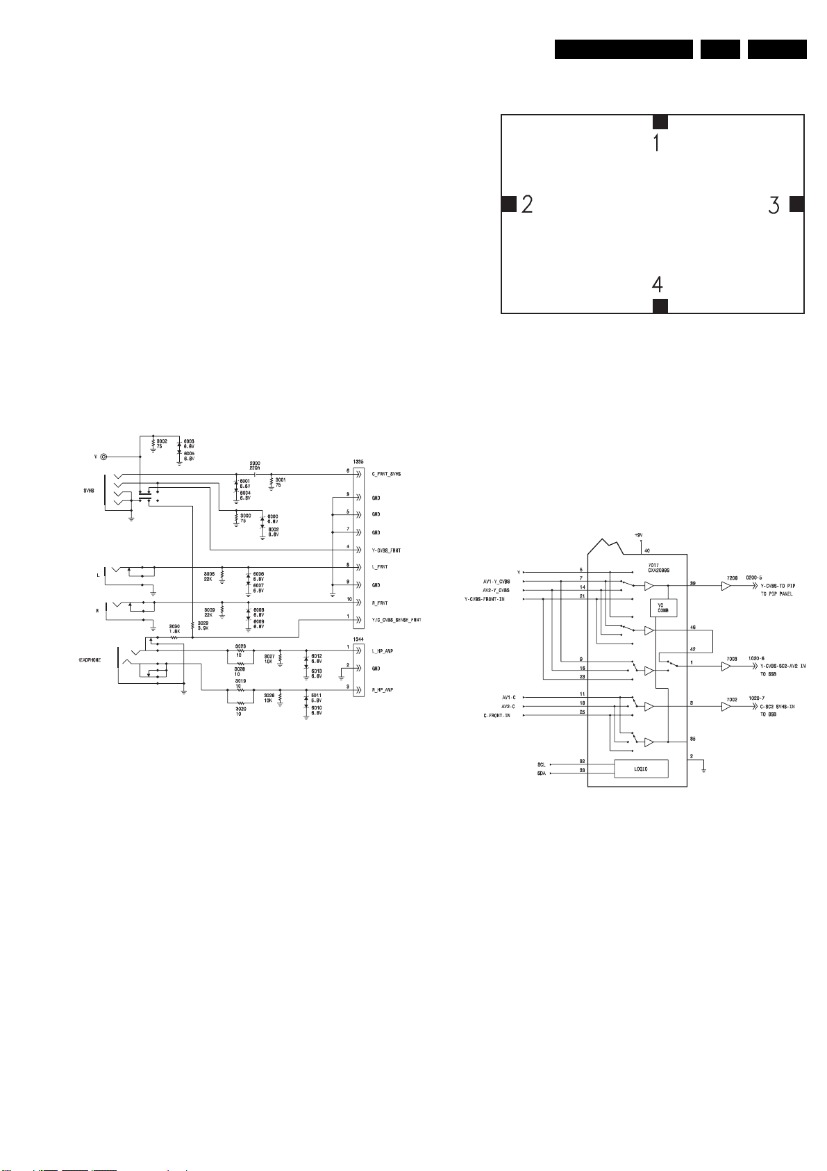
Circuit Descriptions, List of Abbreviations, and IC Data Sheets
EN 85DPTV465 9.
doubler circuit on the SSB, called the Feature Box, changes the
interlaced 625 or 525 signal to a Progressive Scan 480p, 576p,
100Hz, or 120 Hz signal. This YUV signal is buffered and fed to
the SSM where it is buffered before being fed to the HOP (High
end Output Processor) panel. The HOP panel has the HD input
jacks and DB15 RGB input. These inputs can be either 480p,
576p, or 1080i. The Video processing circuits on this panel
perform the Colour, Tint, Brightness, and Contrast adjustments
for the video. Signal selections between the signal from the
SSB and the HD inputs are performed on the HOP panel. Sync
processing and selection is also performed on the HOP panel.
Red, Green, and Blue drive from the HOP panel is fed to the
three CRT panels.
There are two sets of connectors, labelled YPbPr. The one on
the SSM is for NTSC signal levels only. The one on the HOP is
for 1080i, 576p, or 480p Progressive Scan only.
1fH Horizontal (Line) and Vertical (Frame) drive from the SSB
is fed to the HOP via the SSM. The HOP panel selects between
the sync from the SSB or the external HD inputs. These signals
are processed on the HOP before being sent to the LSB.
9.3.1 Side Jack Panel
9.3.2 SSM composite Inputs
Figure 9-9 CVBS (composite) video inputs
The composite inputs are located on the SSM. There are two
composite or SVHS inputs. A connector in the SVHS inputs will
mute the composite inputs when the cable in plugged into the
SVHS input. A connector in the SVHS inputs will cause a
voltage change on the SEL-SVHS-RR_STATUS2 line. This will
signal the microprocessor that something is connected to that
input.
E_15000_074.eps
181004
E_15000-073.eps
151004
Figure 9-8 Side Jack circuit
The Side Jack panel has a composite Video and SVHS input.
When there is a connector in the SVHS input, the composite
input is muted. Resistors 3001, 3002, and 3000 on the Video,
Y, and C lines provide 75-ohm impedance matching. If a cable
is plugged into the SVHS connector, the line connecting
resistor, 3029, to ground is removed causing the voltage on the
Y/C_CVBS_SENSE_FRNT line to increase. This signals the
microprocessor to switch the video switching circuits from
composite video to YC In.
There is also a left and right channel audio input.
9.3.3 SSM Video Switching
Figure 9-10 Video switching on SSM
IC 7017, located on the SSM, performs the Video and Audio
switching for the composite inputs to the SSM. Selected Y or
composite video is output on pin 1 before being fed to the SSB.
Selected C is output on pin 3 and is fed to the SSB. Selected
composite Video for the PIP window is output on pin 39 and fed
to the PIP panel. If an SVHS source is selected for the PIP
window, the YC is combined in 7017 and output on pin 39. IC
7017 is controlled by the microprocessor via the I2C SDA and
SCL lines on pins 33 and 32.
E_15000_075.eps
181004
Page 86
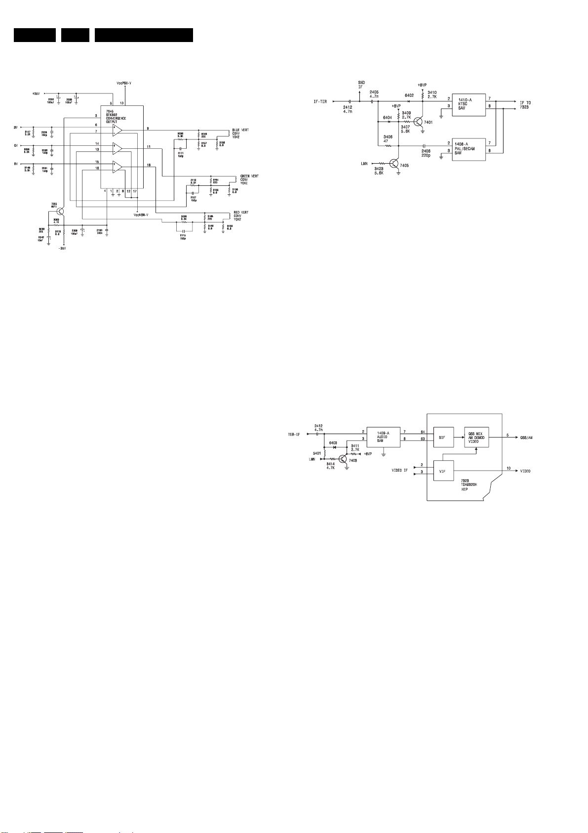
EN 86 DPTV4659.
Circuit Descriptions, List of Abbreviations, and IC Data Sheets
9.3.4 SSB Video Switching
Figure 9-11 Video switching on SSB
Selected composite video from the SSM is fed to the HIP 7323,
located on the SSB. IF from the main Tuner, located on the
SSM, is fed to the SSB via connector 1020 to the switchable
SAW filters 1408 and 1410. Refer to Figure "SAW filter
switching circuit" for description of the SAW circuits. IF from the
SAW filters is then fed to Pins 2 and 3 of 7323. composite Video
is output on pin 10 and is buffered by 7411. Video is then fed to
the switchable Sound traps. Refer to Figure "Sound trap
switching circuit" for a description of the Sound Traps. Output
from the Sound traps is buffered by 7322 and fed to pin 14 of
7323. IC 7323 then selects between the Tuner Video and
selected composite Video or Luminance from the SSM on pin
20. If the signal selected is composite video, it is output on pin
26 and buffered by 7320. It is then fed to the Three Line Comb
filter, 7307. Luminance is output on pin 14 and fed back to 7323
on pin 28. Chroma is output on pin 16 and fed to pin 29. The
internal Chroma switch selects between the output of the Comb
filter or external Chroma on pin 21. Selected Chroma is fed to
the internal Demodulator, which outputs UV to the YUV switch.
Selected Luminance is fed to the internal Delay and to the YUV
switch.
The YUV switch selects between the YUV from the internal
decoder and YUV from the YPbPr inputs located on the SSM.
The microprocessor, located on the SSB, via the I2C buss,
SDA-F and SCL-F, controls the HIP 7323. The YPbPr signals
for NTSC are fed through buffer amplifiers on the SSM before
being fed to the SSB. The selected YUV signal is output on
Pins 49, 50, and 51 to the PIP/DW circuit via connector 1682.
The Y or Luminance signal is fed to the internal Sync Separator
to develop Line and Frame sync. This sync is output on pin 60
and 61. pin 60 is the Line sync while pin 61 is the Frame sync.
Line sync is also output on pin 59 to synchronize the Three Line
Comb filter. When the Component input is selected by the YUV
switch (a DVD player for example), the Y signal is selected by
7017 on the SSM and fed to pin 20 of 7323. The selected Y
signal is then fed to the internal Sync Separator.
E_15000_076.eps
181004
9.3.5 SAW Filter Switching
Figure 9-12 SAW filter switching circuit
The HDR2K3 AP set has a Multi-System tuning system. Since
NTSC uses a 6 MHz bandwidth and PAL/SECAM uses an 8
MHz bandwidth, it is necessary to have separate SAW filters.
The LMN line switches between PAL/SECAM and NTSC.
The LMN line goes "high" in the NTSC mode. Transistor 7405
turns "on" causing a short at the junction of resistor 3406 and
capacitor 2406, removing the signal to the PAL/SECAM SAW
filter (item 1408-A). Transistor 7401 is turned "off". Diode 6402
is forward biased via resistors 3410 and 3406, causing signal
to be applied to pin 2 of 1410-A, and the NTSC SAW filter.
The LMN line goes "low" in the PAL/SECAM mode. Transistor
7405 turns "off", allowing signal to be applied to pin 2 of 1408A, the PAL/SECAM SAW filter. Transistor 7401 is biased "on"
via resistors 3409 and 3407. This prevents the signal from
reaching pin 2 of 1410-A.
9.3.6 3D Comb Filter
Figure 9-13 3D Comb Filter circuit
The 3D Comb Filter is used in NTSC only sets. This is a
separate PC board, which plugs into the System board. The
video signal is buffered by 7008 and 7009. Transistors 7010,
7015, 7016, and 7017 separate the Sync from the composite
video. The Sync is fed to pin 76 of 7023. The composite video
is buffered by 7011 and fed to a 6 MHz filter, 5006. This
prevents any high frequency signals from causing any
problems with the A/D conversion. The signal from 5006 is
buffered by 7012 and fed to pin 88 of 7023. A full frame 3D YC
separation is performed by the YCS circuit. The Y and C
signals are buffered and fed to 6 MHz filters, 5003 and 5004.
The YC signals are then fed back to the SSB via the SSM.
E_15000_077.eps
181004
E_15000_078.eps
181004
Page 87
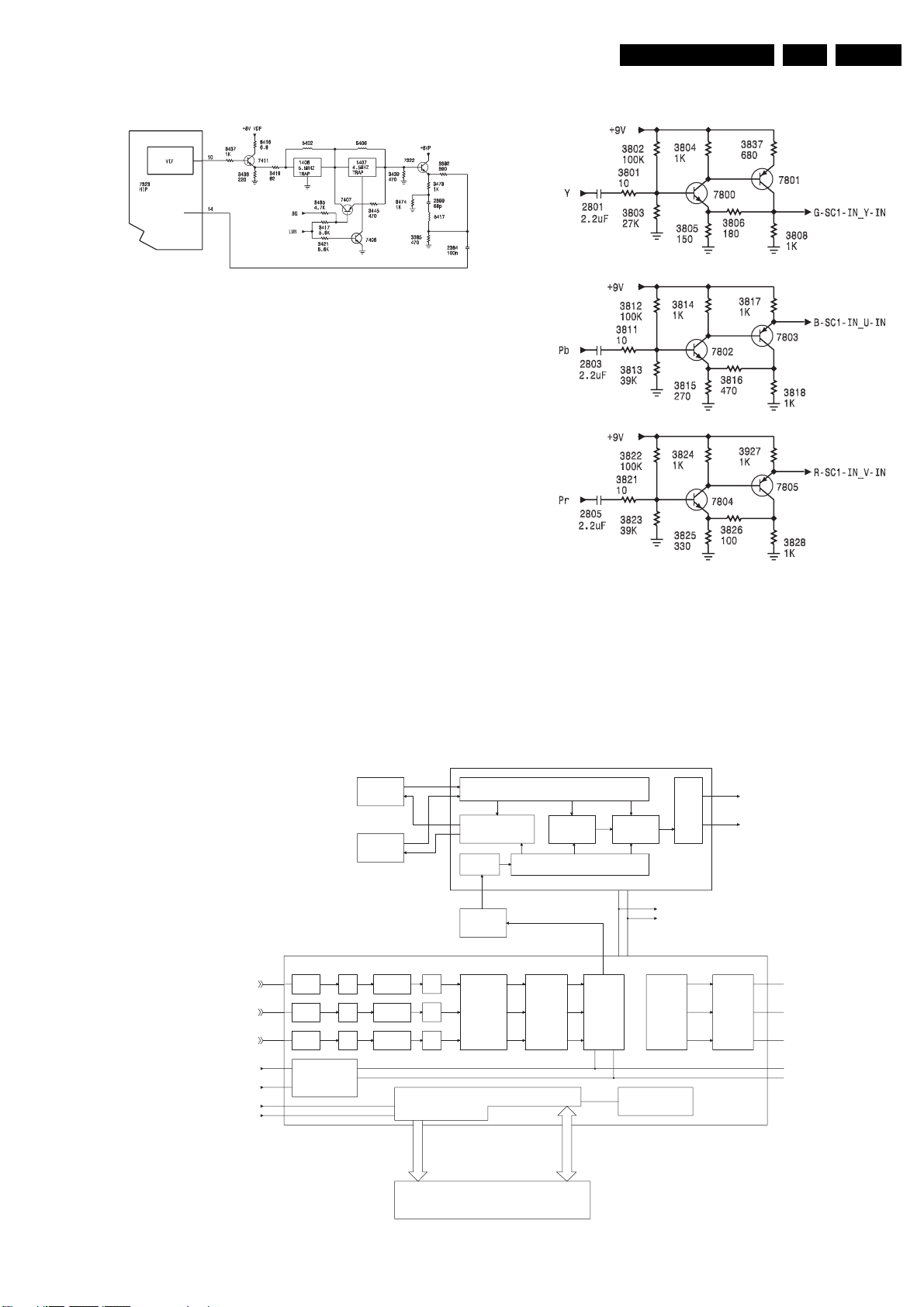
Circuit Descriptions, List of Abbreviations, and IC Data Sheets
EN 87DPTV465 9.
9.3.7 Sound Trap Switching
Figure 9-14 Sound trap switching circuit
Composite video is output on pin 10 of 7323 and buffered by
transistor 7411. The signal is then applied to the 5.5 MHz trap,
1406. In the PAL/SECAM mode, the LMN line is Low, switching
transistor 7407 "on", causing the signal to bypass 1407, the 4.5
MHz filter. The video is then buffered by transistor 7322 before
being applied to pin 14 of 7323.
In the NTSC mode, the LMN line goes "high" and transistor
7406 turns "on", switching the 4.5 MHz SAW filter "on".
Transistor 7407 is turned "off".
E_15000_079.eps
181004
9.3.8 1fH Component Buffer Amplifiers
9.3.9 Feature Box
Y-PIP+MAIN-IN
U-PIP+MAIN-IN
V-PIP+MAIN-IN
SCL-F
SDA-F
HA50
VA50
E_15000_080.eps
181004
Figure 9-15 Component (YPbPr) buffers
The Y signal is buffered by transistors 7800 and 7801. This is
an impedance matching and YPbPr to YUV circuit. This circuit
does not invert the signal. The Pb signal is amplified by 7802
and buffered by 7803. The Pr signal is amplified by 7804 and
buffered by 7805. The Pb and Pr signals are inverted.
E
D
C
B
A/D
A/D
A/D
16b
16b
16b
DE-INTERLACER
16b
DYNAMIC
NOISE
REDUCTION
7714
FM1
TIME
BASE
CORRECTION
MICROCONTROLLER CORE
MP
MOTION
ESTIMATOR
MF
16b
NOISE
REDUCTION
HISTOGRAM
UPCONVERSION
7718
27
SN-CL
2
PROGRAM
ROM
FALCONIC
SAA4992
TO EAGLE
BUS D
TRIPLE
DAC
MP
26
SN-DA
1
BUS C
MUX
VERT
PEAK
F
G
7611
PICNIC
SAA4978
16b
16b
TRIPLE
ANALOG
FILTER
TO
EAGLE
12
14
NOT
USED
15
18
19
7719
FM3
7717
FM2
1682
6
23
8
25
9
26
28
29
4
5
CLAMP
CLAMP
CLAMP
SYNC
PROCESSING
AGC
PREFILTER
AGC
PREFILTER
AGC
PREFILTER
ADDRESS
7716
EPROM
DATA
Figure 9-16 FBX block diagram
E_15000_084.eps
181004
Page 88
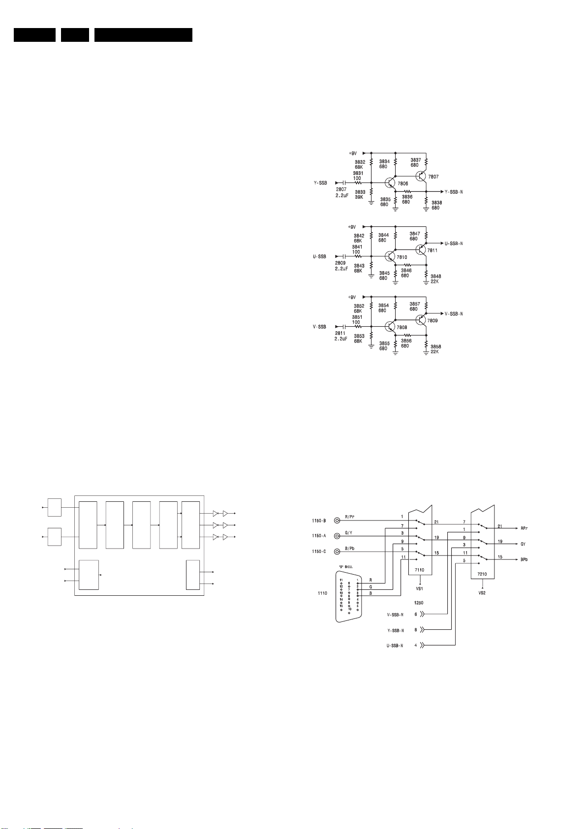
EN 88 DPTV4659.
Circuit Descriptions, List of Abbreviations, and IC Data Sheets
The circuit located on the SSB labelled the Feature Box
performs the digitising, line doubling, and picture resizing. The
main functions are performed by 7611, PICNIC (PICture
improvement Network IC), and 7718, FALCONIC (Field And
Line Converter and Noise reduction IC). The PICNIC IC
performs the A/D Analogue-to-Digital conversion while the
FALCONIC performs the Line Doubling. The FALCONIC also
performs the Super Zoom, Panoramic, 4:3, Movie Expand
14:9, Movie Expand 16:9, 16:9 Subtitle, and Widescreen
picture format conversions.
The YUV signal is fed to the PICNIC on Pins 23, 25, and 26.
Horizontal and Vertical Sync is fed to the IC on Pins 28 and 29.
The signals are fed to a Clamping circuit to limit the sampling
range, an AGC, and a Prefilter circuit. It is then fed to a triple A/
D converter, Time Base Corrector, Noise Reduction and
Histogram circuit, and a Multiplexer. The Prefilter circuit limits
the bandwidth of the signals to prevent aliasing. Aliasing shows
up as artefacts in the picture, which is caused by under
sampling. The Multiplexer combines the three data streams.
Data is output from the PICNIC to FM1 (Field Memory), IC
7714. The Fields are ready by 7718 to the Dynamic Noise
Reduction circuit and to the processor. The De-Interlace writes
the Field data to Field Memory 2, 7717 and Field Memory 2,
7719. The Processor then reads the Field memories to convert
the signal to a progressive scan signal. A Motion Estimator
processes moving blocks in the picture to produce a natural
motion. The processors resize the picture to fit the format
selected by the user. However the picture appears to be
formatted, the output is always a 480P or 576P format. The
Signal is output on two 16-bit busses, F and G, to the Eagle
processor.
The FALCONIC is controlled by the microprocessor in the
PICNIC. The PICNIC is controlled by the Fast clock and data
line from the OTC. The PICNIC communicates with the
FALCONIC and the Eagle via the SN clock and data line. This
is called a SNERT interface. SNERT is a No parity Eight-bit
Reception and Transmission interface.
Horizontal and Vertical sync is output on Pins 18 and 19.
9.3.10 Eagle
available. The signal is converted to an analogue format and
output on Pins 54, 63, and 73. Sync is output on Pins 28 and
29. The signal is then fed to a buffer circuit on the SSM and
then to the HOP. The Eagle is controlled by the microprocessor
in the PICNIC IC via the SNERT interface. The Eagle outputs
an analogue YUV signal to the SSM (Small Signal Module).
9.3.11 SSM HOP Buffer Amplifiers
E_15000_086.eps
181004
Figure 9-18 SSM YUV-buffers
The Y-SSB, U-SSB, and V-SSB signals are fed to buffer
amplifiers, located on the SSM. Transistors 7806 and 7807
buffer the Y signal. The U signal is buffered and inverted by
transistors 7810 and 7811. The V signal is buffered and
inverted by transistors 7808 and 7809. The YUV signal is then
fed to the HOP panel via connector 1250.
9.3.12 HOP RGB/YUV Switching
16b
7722
F
FM4
VERT
INPUT
HORIZ
MUX
SNERT
PEAK
CONTROLS
16b
7723
G
FM5
SN_CL
INERFACE
SN_DA
SCALING
7724
EAGLE
YUV
FORMAT
7731
7728
54
D/A
63
73
28
SYNC
29
7732
7733
HD_E
VD_E
Y_EAGLE_E
7729
U_EAGLE_E
7730
V_EAGLE_E
E_15000_085.eps
181004
Figure 9-17 Eagle
The Eagle circuit provides Skin tone correction, Blue stretch,
and Green Enhancement. In versions, equipped with the Pixel
Plus feature, the Eagle IC performs the corrections for this
mode.
The video frames are sent to FM4 and FM5, 7722 and 7723,
memories from the FALCONIC IC. These memory ICs hold the
frame data until they are required for processing by the Eagle.
The Input Multiplexer selects which frame is to be read. The
Vertical and Horizontal Peaking circuit sharpens the edges and
adds blue pixels to enhance the picture. This circuit is part of
the Pixel Plus processing.
The Scaling circuit scales the picture to a 100 Hz Digital Scan,
75 Hz Digital Scan, 576 progressive, or 480p progressive. If the
input signal is from an NTSC source, only 75 Hz or 480p is
E_15000_087.eps
181004
Figure 9-19 RGB/YUV switching
The input to the HOP panel can be RGB or YPbPr via the cinch
connectors or the Sub-D connector. This connector is not
present in the Basic or Basic Plus versions. The RGB or YPbPr
signal can be either 480P progressive scan or 1080i interlaced.
IC 7110 selects between the R/Pr-G/Y-B/Pb and the RGB
signal from the Sub-D connector. The output of 7110 is fed to
7210, which selects between the output of 7110 and the YUV
signal from the SSM.
Page 89
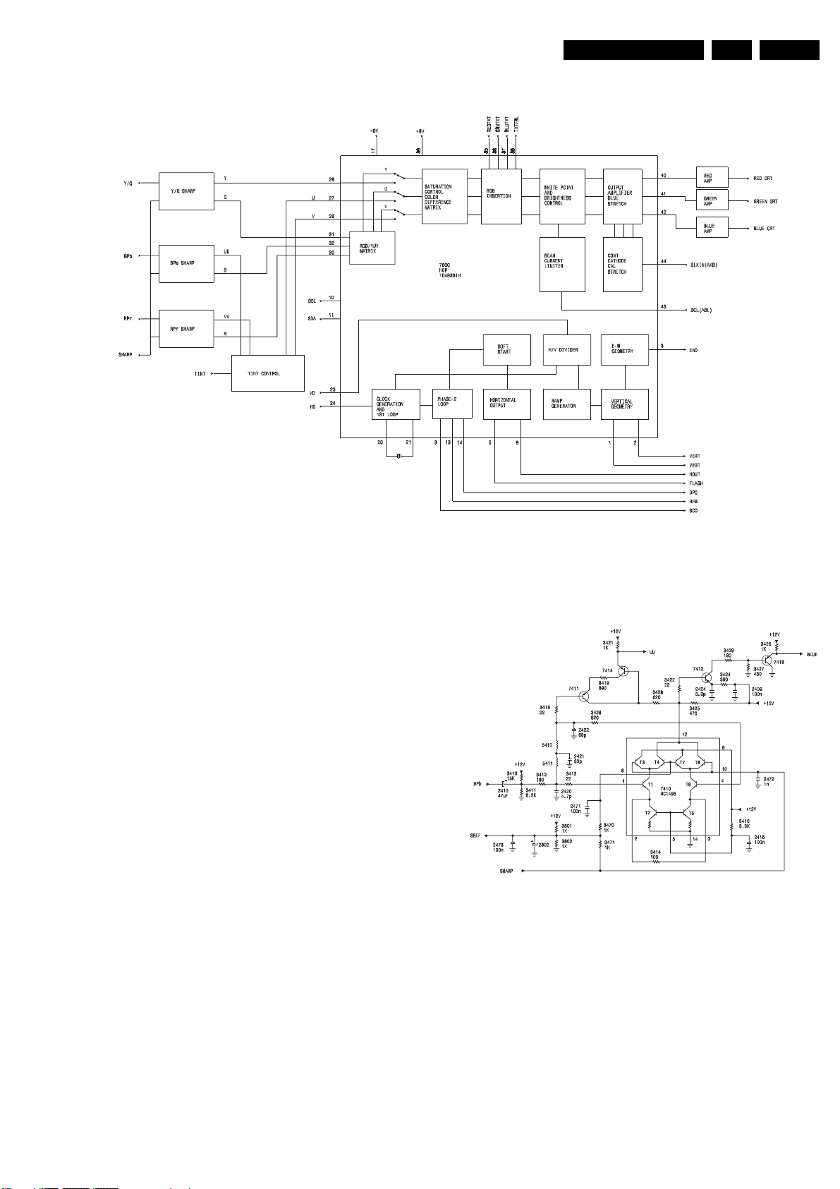
Circuit Descriptions, List of Abbreviations, and IC Data Sheets
9.3.13 HOP Signal Processing
EN 89DPTV465 9.
Figure 9-20 HOP signal processing
The Y/G, B/Pb, and R/Pr signals are fed to their respective
sharpness controls. If the input is a YUV signal, the Y signal is
fed to pin 28 of 7600. The U and V signals are fed to the Tint
Control circuit and then to Pins 27 and 26 of 7600. If the input
is RGB, the signals are fed to Pins 31, 32, and 30 of 7600 to an
RGB to YUV converter. When RGB input is used, there is no
Tint control available for the signal.
The input selector switch in 7600 selects between the YUV on
Pins 28, 27, and 26 or the output of the internal RGB/YUV
converter. The signal is fed to the RGB insertion circuits where
the OSD is inserted. The signal is then fed to a White Point
circuit and then to the Output Amplifier. The White Point and
Output Amplifier have the Drive controls and Cut-off controls.
Input from the ABL line on Pins 43 makes adjustments in the
brightness levels to adjust for changes in beam current. The
AKB pulses from the CRTs are fed to pin 44 to the Cathode
Calibration circuit. The Cathode Calibration circuit adjusts the
Cut-off levels of the CRTs to maintain the correct grey scale
tracking. When the set is first turned "on", a calibration pulse is
output on the RGB lines. The Cathode Calibration circuit
monitors this pulse on the AKB line to set the Black level and
the maximum drive voltage for the cathode. Once the
Calibration has taken place, the Output Amplifiers switches to
the RGB drive signal as the output.
Horizontal and Vertical Sync is fed to 7600 on Pins 23 and 24.
IC 7600 processes the sync to provide the geometry for the
picture. Horizontal drive is output to the sweep circuit on pin 8.
Vertical drive is output on Pins 1 and 2. East West drive is
output on pin 3. Sandcastle (SCO) is output on pin 9. Horizontal
Feedback (HFB) from the sweep circuit is fed into the Phase
Loop to phase correct the Horizontal drive.
IC 7600 is controlled by the microprocessor via the I2C buss on
Pins 10 and 11. Geometry and Drive settings are stored in the
Memory IC located on the HOP panel.
E_15000_088.eps
9.3.14 HOP Sharpness Control
Figure 9-21 HOP sharpness control
The Sharpness controls for the YUV/RGB signals are located
on the HOP panel. Since all three circuits are basically the
same, only the Blue one will be discussed.
The Blue signal is fed to pin 1 of 7410. It is also fed to a Low
Pass filter consisting of 5411 and 5410. This path is amplified
by transistor 7411. The Low Pass filter blocks the higher
frequencies as well as shifting the phase of the signal. The
output of the Low Pass filter is also fed to pin 4 of 7410. The
mixing of these two-phase shifted signals only allows the High
frequency component to be amplified and output on pin 12. The
gain of the High frequency component is controlled by the
Sharpness voltage, which is applied to Pins 8 and 10. The two
signals are combined at pin 12 of the IC. If the input was a Blue
181004
E_15000_089.eps
181004
Page 90
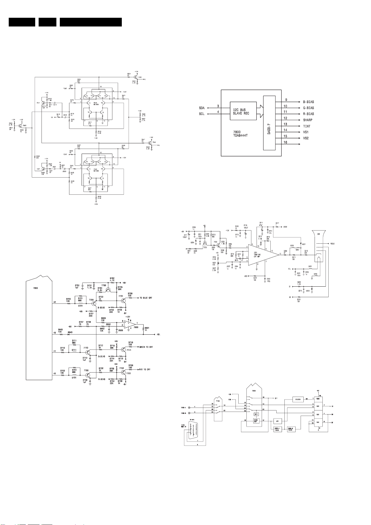
EN 90 DPTV4659.
Circuit Descriptions, List of Abbreviations, and IC Data Sheets
signal, it is amplified by 7412 and buffered by 7413. If the input
was a U signal, it is buffered by 7414.
9.3.15 HOP Tint Control
Figure 9-22 HOP tint control
E_15000_090.eps
181004
Green and Red CRTs, the inverting input on pin 2 will become
greater than the non-inverting input on pin 3, resulting in the
output on pin 1 to go Low. The ABL line will go Low, causing
7600 to reduce the drive to all of the CRTs. This circuit prevents
the Blue tube from being over-driven.
9.3.17 HOP Analogue Control
E_15000_092.eps
Figure 9-24 IC7800 HOP analogue control
IC 7800 develops the analogue control voltage for the HOP
panel. The I2C bus controls the IC. This IC is located on the
HOP panel.
9.3.18 CRT Panel
181004
IC 7510 amplifies the U signal while 7520 amplifies the V
signal. The Tint control voltage changes the balance between
the U and V signals to change, causing the tint of the picture to
change.
9.3.16 HOP RGB Amplifiers
Figure 9-23 HOP RGB amplifiers
The output of 7600 is fed to the RGB amplifiers before being
fed to the CRTs. Transistors 7720 and 7721 buffer the Blue
output on pin 42. The B-BIAS control voltage controls the gain
of this circuit. Transistor 7730 provides an additional voltage
gain for the signal.
Items 7710 and 7711 buffer the Green output from pin 41 of
7600. The G-BIAS controls the gain of the circuit.
The Red output from pin 40 of 7600 is buffered by 7700 and
7701. The R-BIAS controls the gain of the circuit.
The drive of the Red and Green outputs is compared with the
Blue drive by 7900-A. The difference signal is fed back to 7600
via the ABL line. If the Blue CRT is driven harder than the
E_15000_091.eps
181004
Figure 9-25 RGB amplifiers on CRT panel
The Red, Green, and Blue signals from the HOP panel are fed
to their respective CRT panel. The signal is fed to the emitter of
7200 and then to 7202 on each panel. The output of 7202 is fed
to pin 2 of 7201, which drives the cathode of the CRT. AKB
drive is output on pin 7 and fed to the HOP panel.
9.3.19 HOP Sync Switching and Processing
Figure 9-26 HOP sync processing
Horizontal and Vertical Sync from the SSB is fed to the HOP
panel via the SSM panel, when NTSC is used as the signal
source. In sets with the D Shell RGB input, 7110 switches
between the Vertical and Horizontal Sync on the cinch
connectors or the Sync from Pins 13 and 14 of the D Shell
connector. IC 7210 selects between the output of 7110 and the
E_15000_093.eps
181004
E_15000_094.eps
181004
Page 91
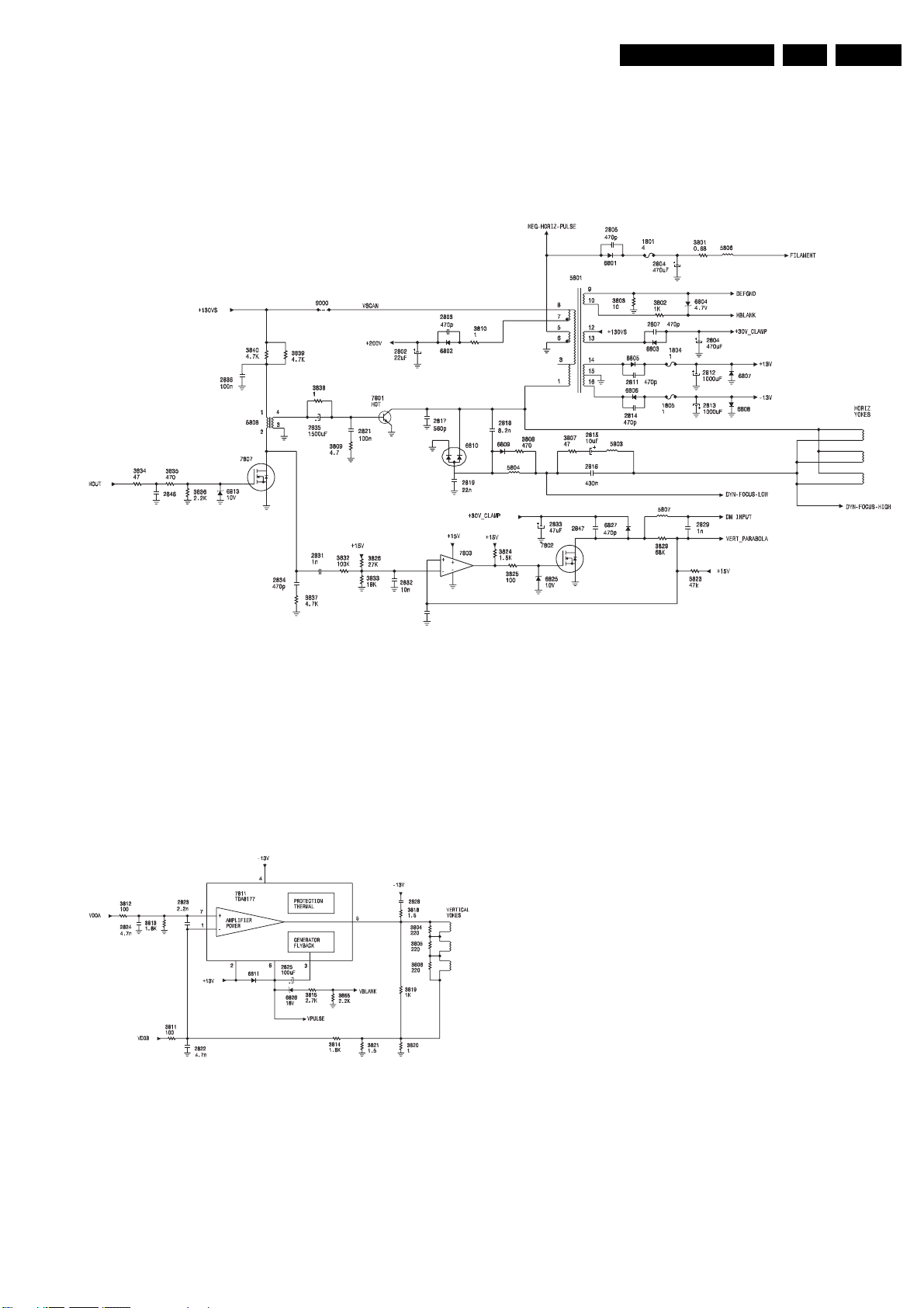
Circuit Descriptions, List of Abbreviations, and IC Data Sheets
EN 91DPTV465 9.
Sync from the SSB. For separate Horizontal and Vertical Sync,
the output of 7210 is fed to the multiplexer IC 7330, which is
used as a switch. In the case of Sync on Y or Sync on Green,
pin 19 of 7210 is fed to pin 18 of 7210 to a Sync Separator. If
separate Horizontal Sync is present, the internal detector in
9.3.20 Line Output
7210 turns the Sync Separator "off". The Sync output on pin 17
is fed to a Low Pass Filter, which separates the Vertical Sync.
The Timer IC 7328 detects the Horizontal Sync and feeds it to
7330. The detected Horizontal Sync from 7328 is fed to pin 1 of
7330 to switch the IC to the pin 6 and 3 inputs.
Horizontal drive from the HOP panel is fed to 7807 on the Large
Signal panel. Transistor 7807 drives the Horizontal Output
Transistor 7801, which drives the Yokes and the Horizontal
Output Transformer 5801. Transformer 5801 produces plus
and minus 13-Volt supplies for the Vertical Output circuit. It also
produces a 200-Volt source and Filament voltage for the CRT
panels. The output of 7807 also drives 7803 and 7802, which
drives the Dynamic Focus circuit.
9.3.21 Frame Amplifier
E_15000_095.eps
181004
Figure 9-27 Line output circuit
E_15000_096.eps
181004
Figure 9-28 Frame circuit
The Vertical drive from the HOP panel drives the Vertical
Output IC 7811. This IC is located on the Large Signal panel.
Drive is fed to pin 7 and is output on pin 5 to drive the three
Vertical Yokes. This IC is powered by the plus and minus 13Volt supplies from the Horizontal Output circuit. A Vertical pulse
on pin 6 is fed to the sweep failure detection circuit. If there is
a failure in the Horizontal or Vertical sweep, the High Voltage
will be shut down.
Page 92
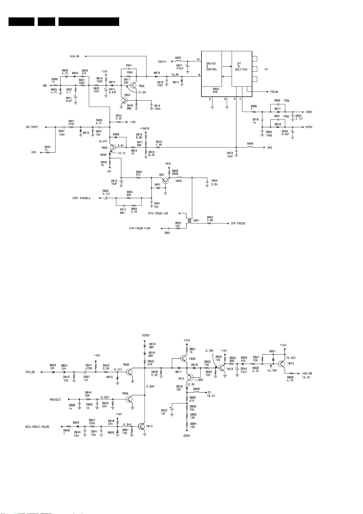
EN 92 DPTV4659.
9.3.22 High Voltage Circuit
Circuit Descriptions, List of Abbreviations, and IC Data Sheets
The High Voltage module is an integrated High Voltage supply
with its own switching power supply. When the set is turned
"on", 11.5 volts from the Sweep Failure detection circuit is fed
to diode 6913 and to pin 8 of the High Voltage module. A supply
voltage of 130 volts is also fed to pin 10 of the module. The
Module then outputs High voltage to the three CRTs. It also
outputs Focus voltage to the Focus G2 block. Output on pin 4
is rectified by 6917 to produce a negative 200 Volt source for
the CRT G1 voltage. The voltage is also rectified by 6919 to
9.3.23 Shutdown
E_15000_097.eps
181004
Figure 9-29 High voltage circuit
produce a 375 Volt source for the Dynamic Focus drive. The
DAG line along with the output on pin 2 is connected to 7903 to
produce the ABL voltage for the set. If an over-current condition
should develop with the drive, the ABL voltage will go Low,
turning 7905 "on", latching 7904, which will remove drive to pin
8 of the HVG. This will cause the High voltage to shut "off".
Vertical Parabola drive is fed to 7901 to produce the Vertical
component of the Dynamic Focus drive.
Figure 9-30 Blanking and HV-protection circuit
The Shutdown circuit will shut the High voltage "off" if the
Horizontal or Vertical Sweep should fail. It will also shut the
High voltage "off" if the Power Fail line goes "high" or the +200
Volt source should fail.
E_15000_098.eps
181004
The Vertical pulse is fed to zener diodes 6824 and 6814, which
keeps capacitor 2837 charged. This pulse is rectified by 6815
to keep the base of 7808 at a negative voltage. This keeps the
Page 93
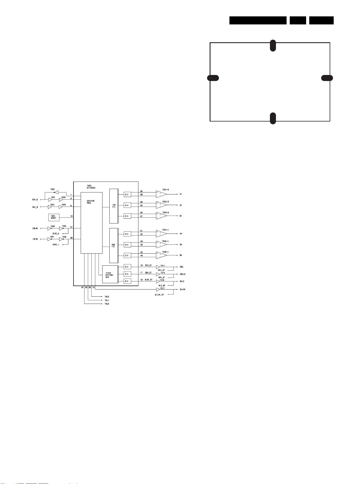
Circuit Descriptions, List of Abbreviations, and IC Data Sheets
EN 93DPTV465 9.
transistor turned "off". In the same manner, the Negative
Horizontal pulses keep the base of 7810 at a negative voltage
to keep it turned "off". The Protect line is normally Low, keeping
7809 turned "off". The +200-volt source is fed through zener
diodes 6812 and 6816, resistor 3850, the base-emitter of 7906,
the base emitter of 7812 to keep transistor 7813 turned "on".
This turns transistor 7814 "on", which switches the "on" voltage
to the High Voltage module. The conduction of 7812 keeps the
voltage on the G1 line at approximately - 18 Volts, which turns
the CRTs "on". If the Vertical Pulse should fail, transistor 7808
will turn "on", which will turn 7906, 7812, 7813, and 7814 "off".
This will turn the HVG module "off". In addition when 7812 turns
"off", the G1 voltage will go to -200 Volts, blanking the CRTs.
The same sequence will occur if Horizontal should fail, the
Protect line should go "high", or the +200 Volt source should
fail.
9.3.24 Convergence
The Convergence system is split into two sections. The
convergence signal processor is located on the ACS (Auto
Convergence System) module. The output amplifiers are
located on the SSM (Small Signal Module).
Convergence processor
Intellisense Sensor Locations
1
2
3
4
E_15000_100.eps
181004
Figure 9-32 Sensor locations
The Philips Intellisense system makes minor Convergence
corrections when the feature is selected by the Customer.
When a PTV is moved from one location to another, minor
Convergence errors will occur due to changes in the Earths
magnetic field. When Save is selected during the Convergence
Alignment, the set scans four optical sensors with each of the
three colours. The locations of these sensors are recorded by
the ACS microprocessor. When the Customer selects the
Intellisense feature, the sensors are again scanned and the
rotation of the beams for each colour is adjusted to the
recorded values.
E_15000_099.eps
Figure 9-31 Convergence signal processor
The Convergence data is stored in the EEPROM, 7000. The
microprocessor located on the ASC module reads 1,971 bytes
of data from 7000 and writes it to the Convergence Processor,
7002. Horizontal sync is inverted by 7026, buffered by 7025,
and fed to pin 27 of 7002. Vertical sync is inverted by 7027,
buffered by 7028, and fed to pin 28 of 7002. The data is
processed to produce the desired convergence correction
waveforms, which are output on six DACS. During the
convergence adjustment procedure, a 180-point alignment grid
is output on Pins 16, 17, and 18. This signal is mixed with the
OSD to be displayed on the screen. In the 4x3 aspect ratio set,
there are three sets of convergence data. In sets with a 16x9
aspect ratio, there are two sets of convergence data. The set
will require convergence alignment for each set of convergence
data. The correct mode must be selected and the signal for that
mode must be applied to the set during the convergence
alignment. The output of the DACS is fed to six op-amps before
being fed to the Power Amplifiers located on the SSM. When
screen centring is being performed, it is necessary to disable
the convergence drive waveform. A High on pin 77 turns
transistor 7029 "on", turning 7038 "on", which turns transistors
7032, 7033, 7030, 7031, 7034, and 7035 "on". This mutes the
correction drive signal to the Power Amplifiers.
181004
Page 94
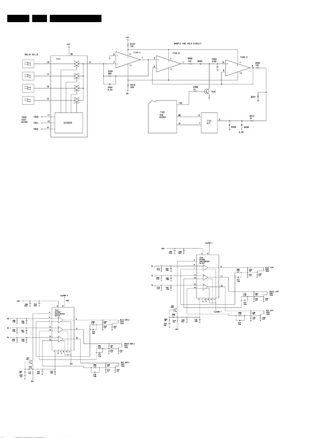
EN 94 DPTV4659.
Intellisense Sensing Circuit
Circuit Descriptions, List of Abbreviations, and IC Data Sheets
Figure 9-33 Intellisense circuit
The output of the four sensing Solar Cells are fed to IC 7141
located on the ACS module. Inputs TBU0, TBU1, and TBU2
from the Convergence microprocessor are fed to the Decoder,
which selects the Solar Cell to be read. The output on pin 3 is
fed to pin 2 of 7140-A. 7140-A matches the low impedance
output of 7141 to the high impedance input of 7140-B. Amplifier
7140-B charges capacitor 2253 with the sample voltage. Due
to the high input impedance of 7140-C, 2253 will hold the
sample voltage until it is cleared by transistor 7540. The output
of 7140-C is fed to 7101, which is an Analogue to Digital
converter. The Digital reference voltage is fed to the ACS
microprocessor where the data is processed and recorded.
When the next location requires sampling, a High is output on
pin 100 of 7100. This turns Transistor 7540 "on" discharging
capacitor 2253.
The Basic version of the HDRPTV does not have the Sensors
installed in the set. However, the Sensor Test is in the Service
Convergence menu. When the Convergence alignments are
stored, the microprocessor will attempt to read the Sensors. If
the Sensor test is selected in the Convergence Alignment
menu, the message will read “Sensors not verified at locations:
1234.” This will not affect the Convergence alignments.
E_15000_101.eps
181004
18. The IC is powered by four supply inputs. A +35 Volt supply
is fed to pin 5, a -35 Volt supply is fed to pin 4, and a -22 Volt
supply is fed to pin 8, 12, and 17. The supply fed to pin 10 is
normally a +22 Volt supply. During signal peak drives, the
voltage on pin 10 is increased to +35 Volts. Feedback sense
voltage is developed across the 6.8 ohm resistors on the return
side of each yoke. Transistor 7007 is part of a Soft Start circuit.
When the set is turned "on", Transistor 7007 turns "on" until
capacitor 2043 is fully charged. While 7007 is being turned
"on", a negative voltage is placed on pin 3 muting the output of
the IC. A 220-ohm snubber resistor is across each of the yoke
windings. This resistor will overheat if the unit is operated with
the Convergence Yokes unplugged.
Convergence Vertical Output
Convergence Horizontal Output
E_15000_103.eps
181004
Figure 9-34 Convergence horizontal output circuit
IC 7044 amplifies the Horizontal convergence waveforms. The
correction waveforms are fed to the IC on Pins 6, 14, and 15.
They are output to the Convergence Yokes on Pins 9, 11, and
E_15000_102.eps
181004
Figure 9-35 Convergence vertical output circuit
IC 7045 amplifies the Vertical convergence waveforms. The
correction waveforms are fed to the IC on Pins 6, 14, and 15.
Output is on Pins 9, 11, and 18 to the Vertical Convergence
yokes. Feedback sense voltage is developed across the 6.8ohm resistors on the return side of each yoke. A Snubber
resistor is across each yoke. These resistors will overheat if the
circuit is operated without the Convergence Yokes being
plugged in. The IC is powered by four supplies, +35 Volt, -35
Volt, VccPSW-V, and VCCNSW-V. The VccPSW-V supply is
normally at +22 volts. The BV_OUT, GV_OUT, and RV_OUT
lines are connected to a Vertical Power up circuit, which
senses the drive to the Convergence Yokes. If the drive to the
yokes reaches 10 to 12 Volts, the Vertical Power up circuit will
switch the VccPSW-V supply to +35 Volts. If the Vertical Power
Page 95
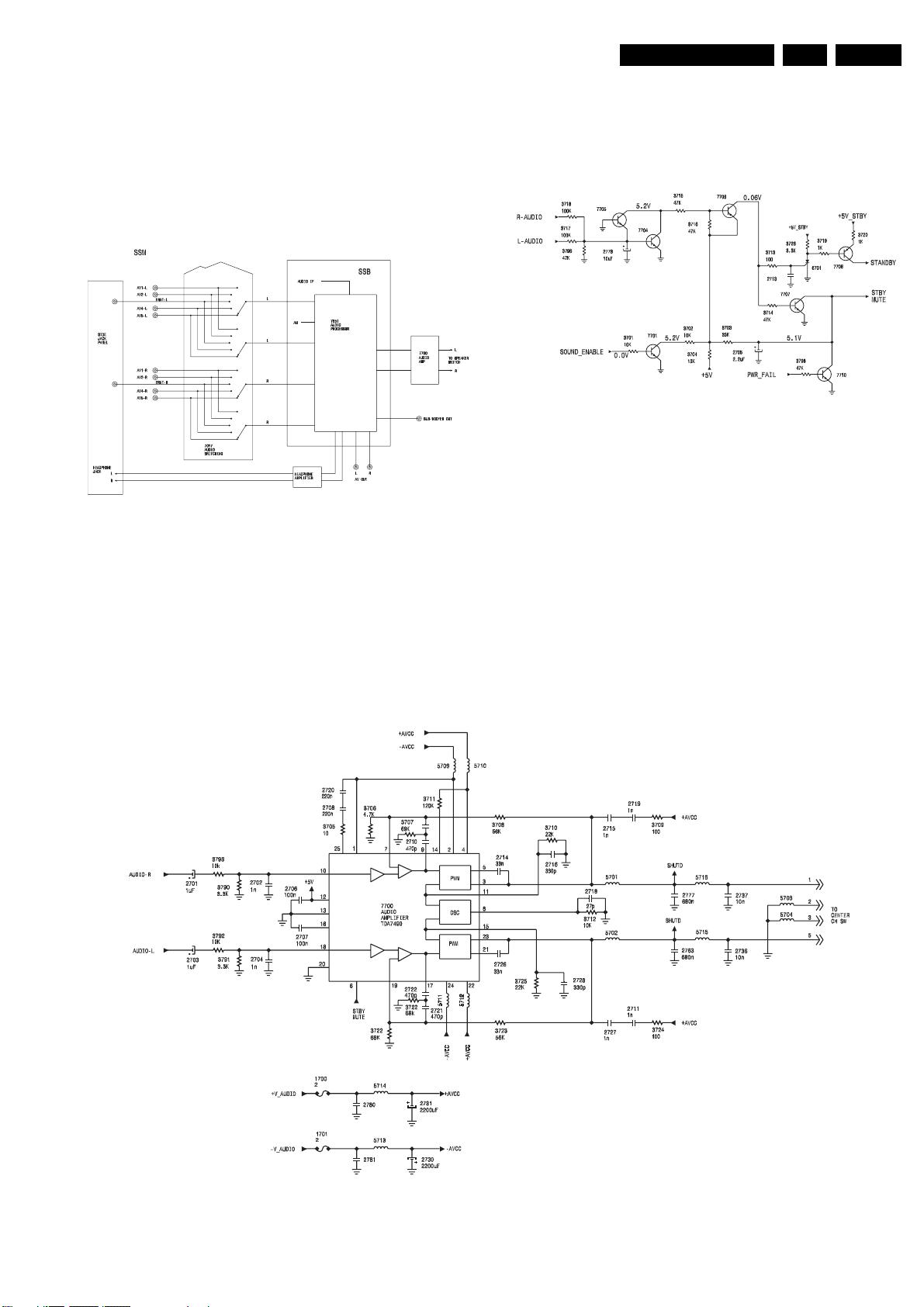
Circuit Descriptions, List of Abbreviations, and IC Data Sheets
EN 95DPTV465 9.
up circuit senses a negative 10 to 12 volt drive to the Vertical
Convergence yokes, the VccNSW-V supply will switch from 22 Volts to -35 Volts. As with the Horizontal drive circuit, 7005
mutes the output of 7045 during power up.
9.4 Audio
9.4.1 Overall Audio Block
Figure 9-36 Overall Audio Block
IC 7017, located on the SSM, selects Left and Right channels
of audio and feeds them to the Audio Processor, 7651, located
on the SSB panel. The Audio processor selects between the
two audio channels from the SSM or internally decoded audio
from selected audio IF on the SSB. The Processor outputs line
level Left and Right monitor audio, and line level Sub Woofer
out. These jacks are located on the SSM. It also outputs Left
and Right audio to the Audio Amplifier, located on the SSM.
E_15000_104.eps
181004
Left and Right audio is output to a Headphone Amplifier located
on the SSM. The output of the Headphone Amplifier is fed to
the Side Jack Panel.
9.4.2 Audio Processor
Figure 9-37 Audio Processor
Audio processing is performed by 7651, which is located on the
SSB. QSS Audio IF is fed to pin 50 of the IC. If the RF signal
source is SECAM, the AM audio is fed to pin 47. Selected AV
audio is fed to Pins 42, 41,45, and 44. The Demodulator
detects and decodes the signal before feeding it to the
processing section. The selected AV audio is fed to two A/D
converters and then to the processing section. The Sound
processing includes Volume, Equalizer, balance, Loudness,
Incredible Sound, and Virtual Dolby. After processing, the
Audio signal is fed to six D/A converters. The Main Speaker
Audio is output on Pins 20 and 21. Headphone Audio is output
on Pins 17 and 18 before being fed to an amplifier on the SSM.
AV out Audio is output on Pins 25 and 26.
E_15000_105.eps
181004
9.4.3 Audio Amplifier
Figure 9-38 Audio Amplifier
E_15000_106.eps
181004
Page 96
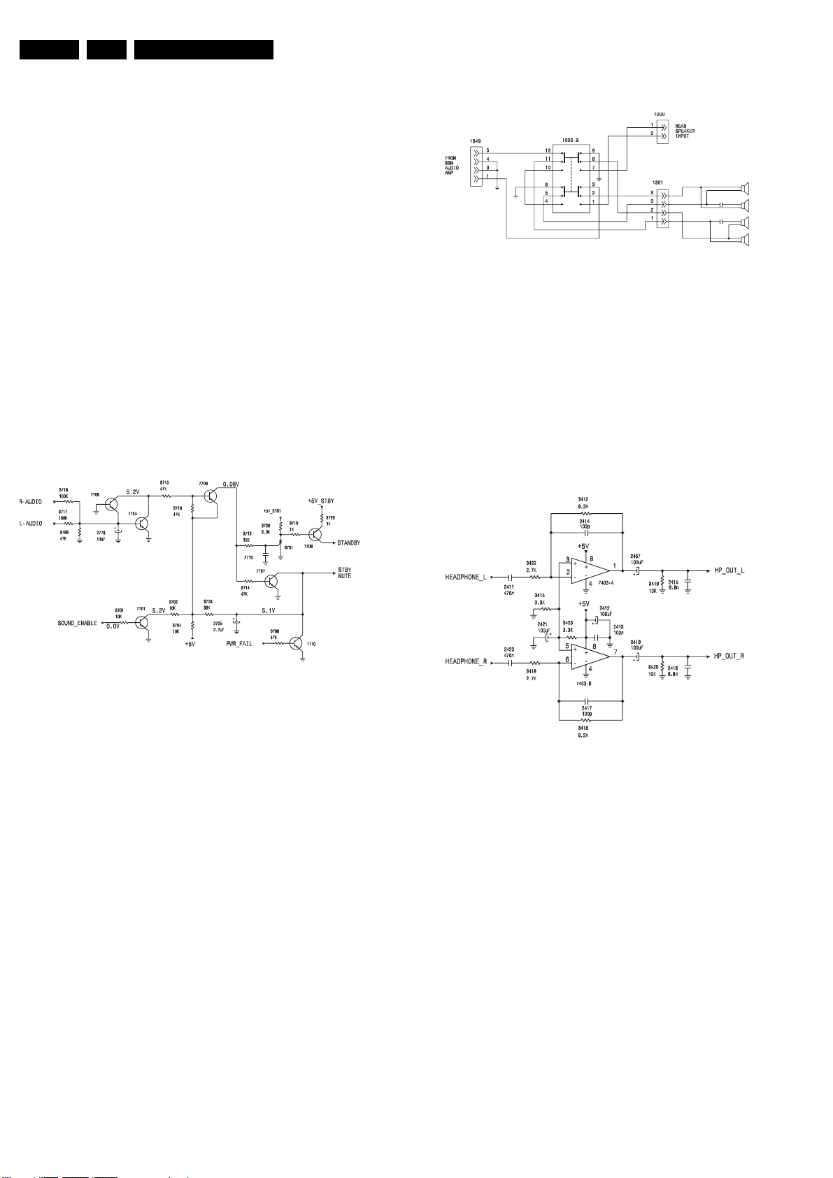
EN 96 DPTV4659.
Circuit Descriptions, List of Abbreviations, and IC Data Sheets
The Audio Amplifier is located on the SSM. The output power
for the Audio Amplifier is 10 Watts per channel for the Basic
and Basic Plus versions. The Core Version has an output of 15
Watts per channel. IC 7700 is the Audio output IC. This is a
class D amplifier. Left and Right Audio from the SSB is fed to
Pins 10 and 18 of the IC. The output stages are basically switch
mode circuits, driven by the audio input signal. The frequency
of the output is keep at 200 kHz by an internal 200 kHz
oscillator. The pulse width of the output is determined by the
signal level of the input signal. The Right Channel pulse width
signal is output on pin 3. The output is filtered by 5701, 2777,
2776, 2717, 5716, and 2737. The amplified audio is output on
connection 1349. In the same manner, Left audio is output on
pin 23. The IC is powered by +19 and -19 Volt supplies. The
supplies are protected by fuses 1700 and 1701. The Supply
voltage for the Core version is 4 volts higher than the Basic and
Basic plus version. The extra supply voltage is needed to
produce the additional 5 Watts per channel output.
Muting and volume control for the audio takes place in the
Audio Signal processor on the SSB. The STBY MUTE line on
pin 6 goes to 2.5 Volts to mute the audio when the set is turned
"on" or "off". This line goes "low" to place the amplifier in a
Standby mode if a DC voltage is detected on the Audio Output
lines.
9.4.4 Shutdown Mute
9.4.5 Centre Channel Amp Switch
Figure 9-40 Centre Channel Amp Switch
The Core versions have a Centre Channel amp switch, located
on the rear of the set. The Output of the Audio Amplifier on the
Basic and Basic Plus versions are fed directly to the speakers.
In the Core sets, the Output is fed to the Centre Channel amp
switch before being fed to the speakers. When the Centre
Channel amp switch is placed in the External position, the Left
and Right speakers in the set are placed in series with the
external speaker input. In cases where the Customer has a
separate sound system, this switch allows the speakers in the
set to be used as the centre output.
9.4.6 Headphone Amplifier
E_15000_108.eps
181004
E_15000_107.eps
181004
Figure 9-39 Shutdown Mute
The Audio Amplifier will be placed in a Standby mode and the
set will shut down if a DC voltage is detected on the Speaker
Output lines. The Left and Right audio output lines are
connected to the base of 7704 and the emitter of 7705 via
resistors 3718 and 3717. Filter capacitor 2778 filters out the AC
component of the waveform. If the DC voltage goes positive,
7704 will turn "on". If the voltage goes negative, 7705 will turn
"on". This turns 7706 "on" which turns 7707 "on". This causes
the Front Detect line to go Low, preventing the microprocessor
from receiving any commands. It also turns SCR 6701 "on",
turning transistor 7708 "on", causing the Standby line to go
"high". If this SCR is turned "on", it will be necessary to remove
power from the set to reset the circuit. This will turn the set "off".
Transistor 7707 also turns "on", causing the Standby-Mute line
to go Low. This places the Audio Output IC in a Standby mode.
If the Power Fail line should go "high", 7710 will turn "on",
causing the Standby-Mute line to go Low.
E_15000_109.eps
181004
Figure 9-41 Headphone Amplifier
IC 7403 is the Amplifier for the Headphone output. The volume
control for the Headphone output is on the Audio Signal
processor located on the SSB. The Headphone Amplifier is
located on the SSM. The output of the amplifier on Pins 1 and
7 is sent to the Headphone Jack, located on the Side Jack
panel.
Page 97
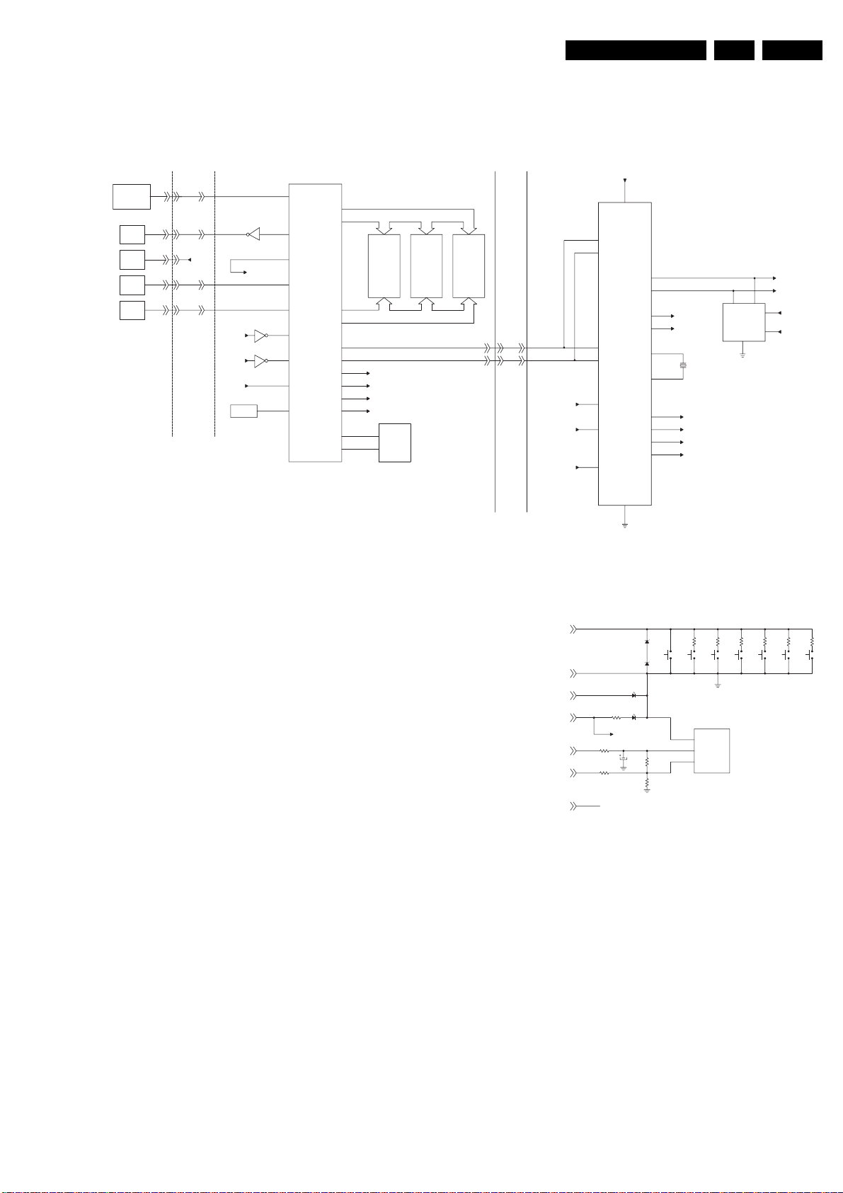
Circuit Descriptions, List of Abbreviations, and IC Data Sheets
9.5 Control/OSD
9.5.1 Microprocessor
EN 97DPTV465 9.
SENSOR
BOARD
KEYBOARD
STBY
LED
ON/OFF
LED
LIGHT
SENSOR
RC5
1201
2
5
4
6
7
1014
2
5
4
6
7
SSM
+9V
1020
79
77
37
78
HFB
VSYNC
CVBS-TXT
RESET
7010
STANDBY
7015
7016
SSB
107
113
104
116
100
83
84
5
74
7001
OTC
SDA
SCL
23-37
DTA
7006
7012
PROGRAM
EPG
FLASH
FLASH-RAM
RAM
45-66
ADD
SDA-S
SCL-S
SDA-F
SCL-F
5
6
7011
NVM
TxD
RxD
90
89
86
85
88
87
91
92
Figure 9-42 Microprocessor
7007
DRAM
TXT
1401-2
1401-4
SSM
1043-9
1043-7
1000-1
1000-2
SYNC-V
SYNC-H
RESET
+3.3V
75
7100
82
ACS
CONTROL
81
16
17
55
53
72
30
ACS
28
13
84
SDA-C
83
SCL-C
69
70
52
BLANK-UP
48
RED-UP
47
GRN-UP
46
BLUE-UP
1200
TO HOP
VIA
SSM
6
7000
NVM
5
1
SDA-B
SCL-B
7
WC
8
+5V
E_15000_110.eps
181004
CONV
PROC
The HDR2K3 has two microprocessors. The microprocessor,
OTC, located on the SSB, 7001, is the main processor for the
set. When Power is applied to the set and the Mains switch is
turned "on", the processor monitors the Keyboard and IR
receiver located on the Sensor Board. This IC controls the
functions on the SSB, Video switching on the SSM, and the
PIP/DW panel. A ROM located inside the IC has the Startup
program. The main program to run the processors is located in
the Program Flash RAM, 7006. IC 7012 is used by the OTC for
temporary storage. IC 7007 is used to store data for Teletext.
There are three I2C busses, a fast bus, F, a slow bus, S, and a
TX bus to communicate with the microprocessor on the ACS
module. The NVM 7011 stores settings such as customer
preferences, OPT numbers, Tuner settings, and Error codes.
composite video is fed to pin 5 for decoding Teletext and
Closed Caption information. In the Standby mode, Power is not
applied to the processor on the ACS module.
The microprocessor, 7100, located on the ACS module,
controls the Convergence, Geometry, and CRT drive circuits.
Settings for Convergence, Geometry, and White drive are
stored in the NVM, 7000. This IC is 512K for the AP sets and
256K for the Korean version. When 7100 reads the size of
7000, it then determines which software to load. If it reads 512K
present, the AP software is loaded. If it reads 256K, NTSC only
software is loaded. Commands for the ACS processor are
produced by the OTC on the SSB and transmitted via the TXD
and RXD lines.
9.5.2 Front Control Panel
KEYBOARD
ON_OFF_LED
+5V_STANDBY
LIGHT_SENSOR
+9V
RC5
GND
1201
2
6102
6.8V
6103
3121
560
3107
330
3109
470
LIGHT_SENSOR
6.8V
RED
6101
GREEN
+9V
3
5
4
1
7
6
VOL-
VOL+
CH+
100
240
3101
3102
1401
3108
6.8K
RC5
3114
10K
1403
1402
1
6105
2
IR
REC
3
Figure 9-43 Front Control Panel
The Front Control panel has the Power LED, Keyboard, IR
Receiver, and Light Sensor. The Keyboard is a resistor ladder.
The voltage changes value depending on which selection is
made. The voltage on this line will be 3.3 volts if no buttons are
selected. The two-colour LED indicates the status of the set. In
the Standby mode, the ON_OFF_LED line is High and the +9volt source is turned "off". In this case, the RED LED is lit.
When the set is turned "on", the +9-volt source is switched "on",
turning the Green section of the LED "on". The LED then turns
Yellow. When the set is fully "on", the ON_OFF_LED line goes
Low, turning the Red LED "off". The indicator is now Green.
The IR Receiver, 6105, receives commands from the remote
control.
MENU
CH-
3103
E_15000_111.eps
ASC
820
470
1404
1.5K
3105
3104
1406
1405
181004
POWER
3.6K
3106
1407
Page 98
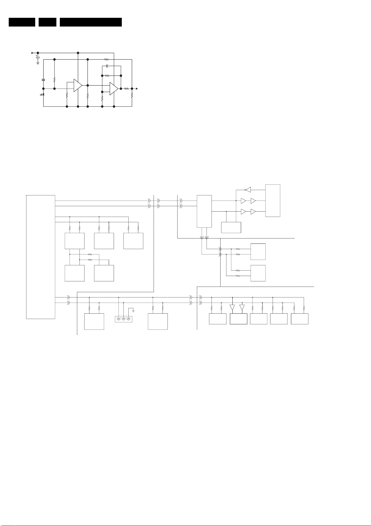
EN 98 DPTV4659.
Circuit Descriptions, List of Abbreviations, and IC Data Sheets
9.5.3 Light Sensor
+9V
2101
10uF
3110
2102
330K
220n
6104
3115
330K
Figure 9-44 Light Sensor
9.5.4 I2C interconnect
90
89
88
SDA-F
87
SCL-F
7001
OTC
86
SDA-S
85
SCL-S
The Light Sensor, 6104, is amplified by two op amps in 7000.
This circuit senses the ambient light and outputs a voltage on
pin 7 of 7000. This voltage is fed to the OTC, which makes
3111
4.7K
2104
9741-C
9741-D
10
5
10
3376
100
1203
TUNER
3117
1K
46
32
2.2uF
3112
3.3K
3113
5
8
+
4.7K
7
6
4
7000-2
3377
100
47
7323
HIP
26
7724
EAGLE
3114
47
4
1
COMPAIR
3118
1K
E_15000_112.eps
3656
100
1
2
7651
MSP
2
3
LIGHT_SENSOR
181004
1401
2
4
3655
100
3131
220
33
7017
AV SW
1043
32
1000
1
2
SSM
3130
220
7000-1
3
8
+
1
2
4
3116
3.3K
SSB
TXD
RXD
3709
3710
100
100
4
5
7713
PICNIC
SN-DA
SN-CL
1
2
26
27
7718
FALCONIC
1020
48
49
3115
47
changes in the picture brightness to compensate for changes
in the ambient light.
7000
GDE
NVM
HOP
7022
7021 7020
7024
3955
100
3956
100
3965
100
3966
100
7832 7829
7801
PIP/DW
7023
7800
I/O
7600
HOP
3267
100
7201
TUNER
7002
CONV
PROC
3268
100
3330
100
7301
SIGNAL PRO
3329 3509
100
E_15000_113.eps
100
7403
I/O EXP
ACS
28
1
2
1201
1
2
SDA-B
7100
ACS
MICRO
13
SCL-B
84
83
1000
6
4
0201
1950
5
SDA-C
4
SCL-C
PIP/DW PANEL
1
2
3431
100
7403
I/O EXP
3432
100
181004
3510
100
Figure 9-45 I2C interconnect
The OTC communicates with the set via three I2C busses.
SDA-F, Fast bus communicates with the PICNIC, HIP, and
MSP (Audio Processor). The SN-DA line from the PICNIC
communicates with the FALCONIC and EAGLE. The SDA-S
Slow bus communicates with the Tuner, AV Switch, and
ComPair connector on the SSM. It also communicates with the
PIP-DW board.
The TXD and RXD lines communicate with the microprocessor
on the ACS module. The microprocessor on the ACS
communicates with the GDE NVM, Convergence Processor,
and the HOP panel.
Page 99
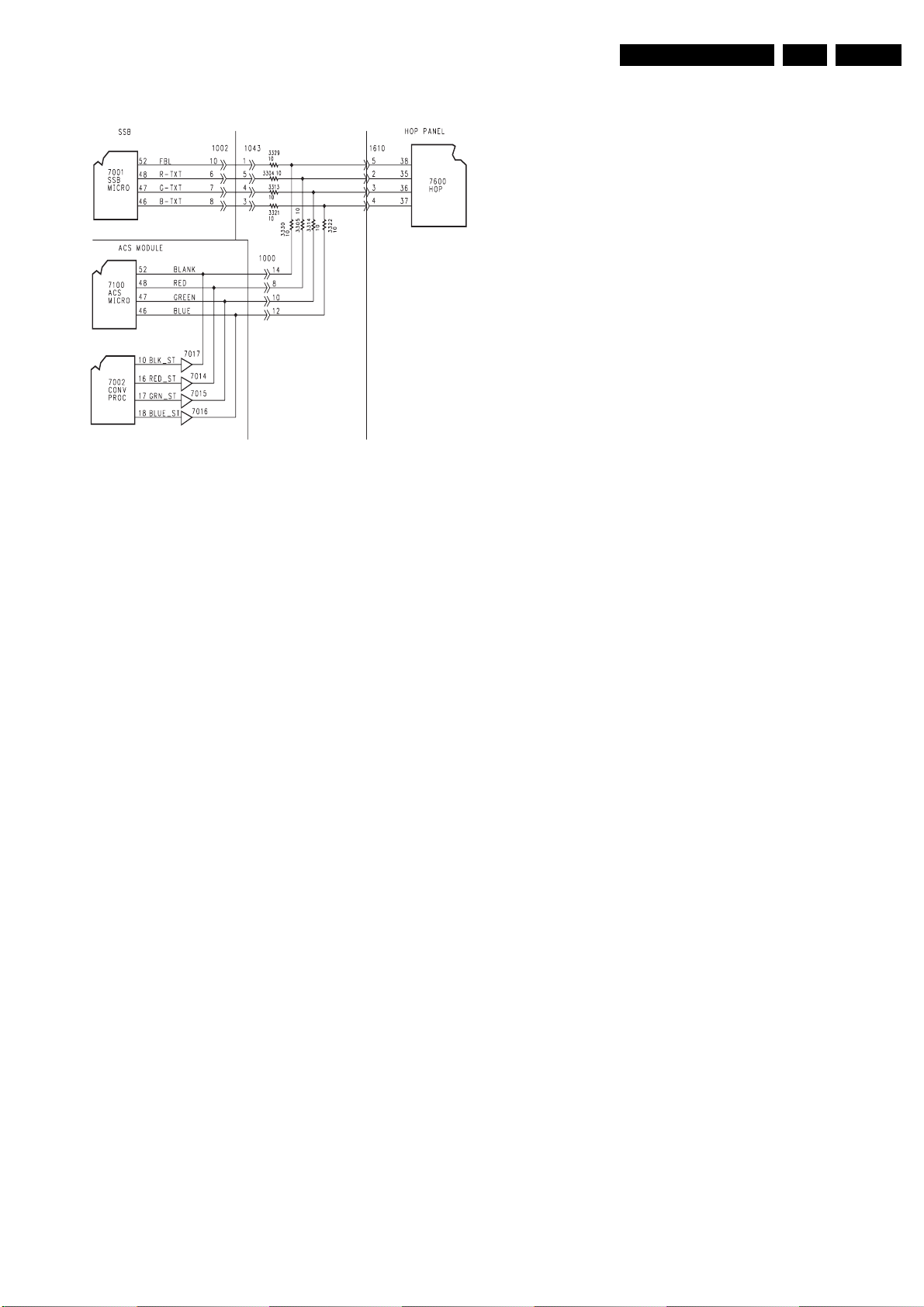
Circuit Descriptions, List of Abbreviations, and IC Data Sheets
EN 99DPTV465 9.
9.5.5 On-Screen Display
Figure 9-46 On-Screen Display
Signal for the OSD (On-Screen Display) comes from three
different sources. IC 7001, which is located on the SSB (Small
Signal Board), generates all of the customer menus except for
Convergence.
In the SAM (Service Alignment Mode), the menus are
generated by 7001, except those in the GDE SAM. The GDE
SAM menus are generated by IC 7100 on the ACS module.
The Convergence Alignment menus are generated by 7100,
while the Convergence Alignment grid is generated by IC 7002.
The OSD signals from 7001 on the SSB are fed to the SSM
(Small Signal Module) via connector 1002 and 1043. The OSD
signals from the Convergence Processor, 7002, are buffered
by 7014 through 7017 before being mixed with the signals from
the ACS microprocessor, 7100. They are fed to the SSM via
connector 1000. The signals from the ACS and SSB are mixed
and fed to the HOP panel and HOP IC, 7600, via connector
1610. The HOP IC, 7600, mixes the OSD signal with the video
signal before feeding it to the CRTs.
E_15000_114.eps
191004
9.6 List of Abbreviations
16:9-ARFRONT 16:9 aspect ratio input from side jack
panel
50Hz/60Hz 50Hz/60Hz AC frequency
6-CHANNEL DAC 6-Channel DAC
ACS Auto Convergence System
AFC Automatic Frequency Control
AGC Automatic Gain Control
AM-FM Amplitude Modulation/Frequency
Modulation
AM-SOUND Amplitude modulated sound signal
AP Asia Pacific
AR Aspect Ratio: 4 by 3 or 16 by 9
ATV See Auto TV
Auto TV A hardware and software control
system that measures picture content,
and adapts image parameters in a
dynamic way
AUDIO_C Audio Centre
AUDIO_L Audio Left
AUDIO_R Audio Right
AUDIO_SL Audio surround Left
AUDIO_SW Audio Subwoofer
AUDIO-L-PROC Audio left processed
AUDIO-R-PROC Audio right processed
AUDIO-SR Audio surround right
AUX-SUPPLY Auxiliary supply
BC-PROT Beam current protection
B/G Monochrome TV system. Sound
carrier distance is 5.5 MHz
BLC-INFO Black current information
B-SC1-IN Blue SCART1 in
B-SC2-IN Blue SCART2 in
BTSC Broadcast Television Standard
Committee. Multiplex FM stereo sound
system, originating from the USA and
used e.g. in LATAM and AP-NTSC
countries
B-TXT Blue teletext
B-vc Blue from video-controller
C Centre
C/16/9 Chrominance input
C-7-OUT Chrominance on pin 7 SCART
(variant)
CBA Circuit Board Assembly
CENTER Centre speaker
C-FRONT Chrominance front input
CL_DS_L Constant Level Dual Screen Left
CL_DS_R Constant Level Dual Screen Right
CL_L Constant Level Left
CL_L_OUT Constant Level Left out
CL_R Constant Level Right
CL-R-OUT Constant Level Right out
CODEC Coding/Decoding
COMP Compander ON/OFF
CORDL_L Cordless Left
CORDL_R Cordless Right
CORE TOP LEVEL Core Top Level
CRT Cathode Ray Tube
CSM Customer Service Mode
C-UI Chrominance UI
CVBS Composite Video Blanking Signal
CVBS_Y-UI CVBS Y UI
CVBS-PIP-DS CVBS Picture In Picture dual Screen
CVBS-SC1-IN CVBS SCART1 in
CVBS-SC2 OUT CVBS SCART2 out
CVBS-SC2-IN CVBS SCART2 in
CVBS-SC3-IN CVBS SCART3 in
CVBS-SC4-IN CVBS SCART4 in
CVBS-TER CVBS terrestrial
CVBS-TXT-DS-OUT CBVBS teletext Dual Screen out
CVBS-TXT-OUT CVBS teletext out
CVBS-Y-FRONT CVBS luminance front input
Page 100

EN 100 DPTV4659.
Circuit Descriptions, List of Abbreviations, and IC Data Sheets
DAC-HOP Digital analogue converter HOP IC
DC_PROT/
AUDIO_SR DC protection (for supply)
DC-filament Filament supply voltage
DC-PROT DC protection
DETECT Detect signal side I/O (side jack panel)
input
DFU Directions For Use: owner's manual
DIG_IN1 Digital In 1
DIG_IN2 Digital In 2
DIGITAL I/O Digital in/out
DIG-OUT Digital out
D/K Monochrome TV system. Sound
carrier distance is 6.5 MHz
DNR Dynamic Noise Reduction
DS-AUDIO-L Dual Sound Audio Left
DS-AUDIO-R Dual Sound Audio Right
DSP Digital Signal Processing
DST Dealer Service Tool: special remote
control designed for service
technicians
DUET DUET-IC
DVD Digital Versatile Disc
DYN-FASE-COR Dynamic phase correction
Eagle Feature box IC performing peaking,
zooming and sub pixel LTI in both
horizontal and vertical directions, CTI,
and other colour features
EHT-INFO Extra high-tension information
EPG Electronic Program Guide (=
NexTView)
EW-DRIVE East-west drive signal
FALCONIC Field and line rate converter IC.
SAA4992H, feature box IC which
performs Digital Natural Motion, 3DNR
vertical zoom, and vertical peaking
FBCSO Fixed beam current switch off
FBL-DS-OUT Fast Blanking Dual Screen out
FBL-FDS Fast Blanking Full Dual Screen
FBL-PIP Fast Blanking PIP
FBL-SC1-IN Fast blanking signal for SCART1 in
FBL-SC2-IN Fast blanking signal for SCART2 in
FBL-TXT Fast Blanking Teletext
FDS Full Dual Screen (same as FDW)
FDSL-OUT Full Dual Screen - Left out
FDSR-OUT Full Dual Screen - Right out
FDW Full Dual Window (same as FDS)
FEAT-U U from Feature Box
FEAT-V V from Feature Box
FEAT-Y Y from Feature Box
FILAMENT Filament of CRT
FILAMENT-PROT Filament protection
FLASH Flash memory
FM Field Memory or Frequency
Modulation
FM SOUND Frequency Modulation Sound
FRAME ROTATION Frame rotation
FRAME-ROT + Frame rotation plus
FRONT-C Front input chrominance (SVHS)
FRONT-DETECT Front input detection
FRONT-Y_CVBS Front input luminance or CVBS
(SVHS)
GDE Generic Display Engine
GHOST-IN Signal Ghost cancellation in
G-SC1-IN Green SCART1 in
G-SC2-IN Green SCART2 in
G-TXT Green teletext
G-vc Green from video-controller
HA Horizontal Acquisition
HA1 Horizontal Sync (diversity)
HA-D Horizontal Sync from HIP-IC to FDS
HD Horizontal drive coming from PICNIC
Hdefl-1in Horizontal deflection signal needed for
DC-shift circuitry
Hdefl-lin Horizontal deflection linearity
HEATER Heater (Filament)
HFB Horizontal flyback
HFB+13V Non-rectified output 13V-winding LOT
HFB-D Horizontal flyback to FDS
HIP High-end Input Processor
HOP High-end Output Processor
HOSD PIP Horizontal OSD PIP
HP Headphone
HS-DS Horizontal sync input POPOV (Double
Window PIP IC)
I Monochrome TV system. Sound
carrier distance is 6.0 MHz
I2C Integrated IC bus
I2S Integrated IC Sound bus
I2S-CL I2S bus clock
I2S-DSP-IN I2S digital signal processor in
I2S-DSP-OUT I2S digital signal processor out
I2S-DSP-OUT1 Serial-DSP-bus-out1
I2S-WS I2S bus Word Stroke
IN-C_IN-R-SC2 Either Chrominance-in SCART2 or
Red-in SCART pin 15
IN-FRONT-SNDL Sound left front in
IN-FRONT-SNDR Sound right front in
IN-SC1-B In SCART1 blue
IN-SC1-G In SCART1 green
IN-SC1-R In SCART1 red
IN-SC1-SNDL In SCART1 sound left
IN-SC1-SNDR In SCART1 sound right
IN-SC2-B In SCART2 blue
IN-SC2-CVBS_Y In SCART2 CVBS or luminance
(SVHS)
IN-SC2-FBL In SCART2 fast blanking
IN-SC2-G In SCART2 green
Interlaced Scan mode where two fields are used
to form one frame. Each field contains
half the number of the total amount of
lines. The fields are written in "pairs",
causing line flicker.
IN-UI-B B input from UI
IN-UI-FBL Fast Blanking input from UI
IN-UI-G G input from UI
IN-UI-R R input from UI
IO-BUS In/out - Bus
IR-LED Drive signal for the service infrared
LED
KEYBOARD Top controls
L Left Audio
LDP Line Deflection Protection
LED Light Emitting Diode
LINE-DRIVE Line drive signal
L/L' Monochrome TV system. Sound
carrier distance is 6.5 MHz. L' is Band
I, L is all bands except for Band I
LMN System L, M, N
LNA Low noise adapter
LS CORRECTION Picture with corrections
LSB Large Signal Board
LV- Frame coil sink signal to the N/S
correction circuitry
LV+ Frame coil drive signal from the frame
output stage
MCADEC_RESET Reset signal (Master reset)
MCS-MPEG Multi Channel Sound - MPEG
M/N Monochrome TV system. Sound
carrier distance is 4.5 MHz
MSP-CLOCK Clock signal multi-standard sound
processor
MUP Microcomputer
MUTE Mute-Line
N52502 CAD naming referring to other sub-
schedule
NC Not Connected
NICAM Near Instantaneous Compounded
Audio Multiplexing. This is a digital
sound system, mainly used in Europe.
 Loading...