

Philips BC559C, BC559B, BC559 Datasheet
DISCRETE SEMICONDUCTORS
DATA SH EET
ook, halfpage
M3D186
BC559
PNP general purpose transistor
Product specification
Supersedes data of 1997 Jun 03
1999 May 28
Philips Semiconductors Product specification
PNP general purpose transistor BC559
FEATURES
• Low current (max. 100 mA)
• Low voltage (max. 30 V).
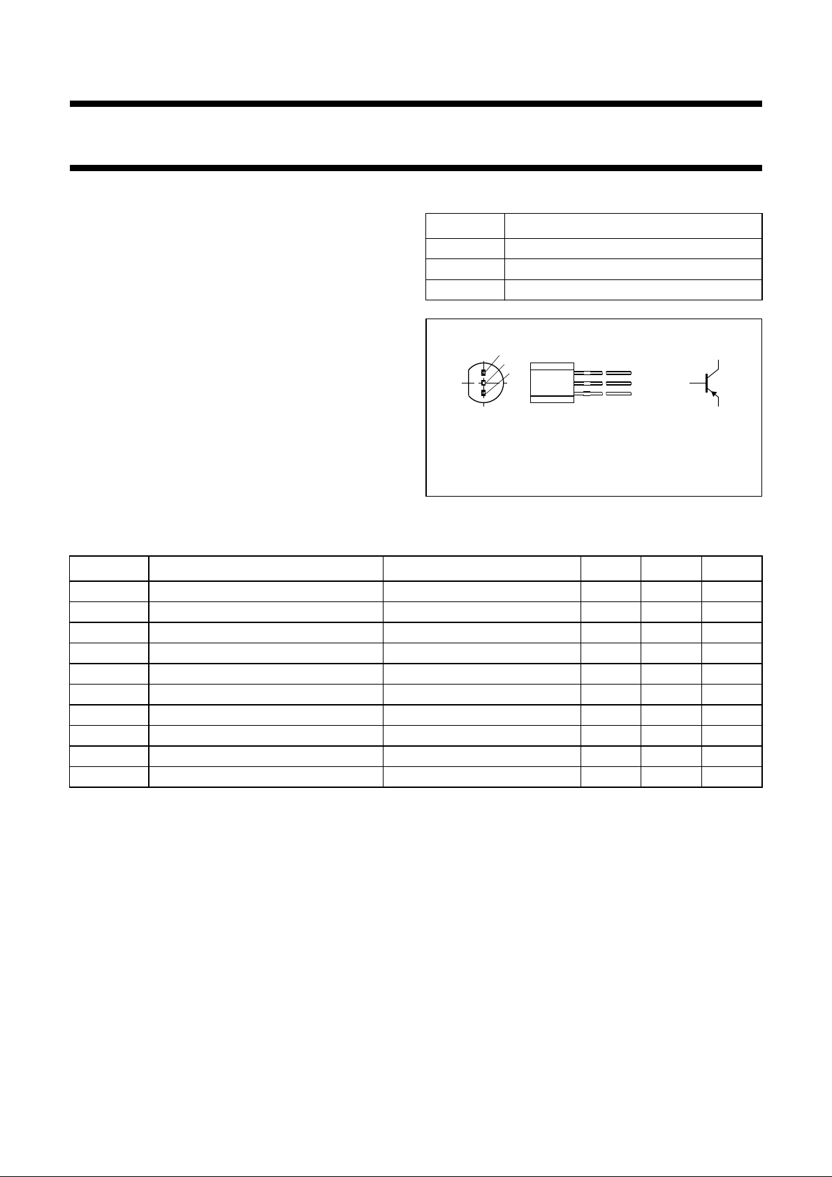
PINNING
PIN DESCRIPTION
1 emitter
2 base
APPLICATIONS
3 collector
• General purpose switching and amplification.
DESCRIPTION
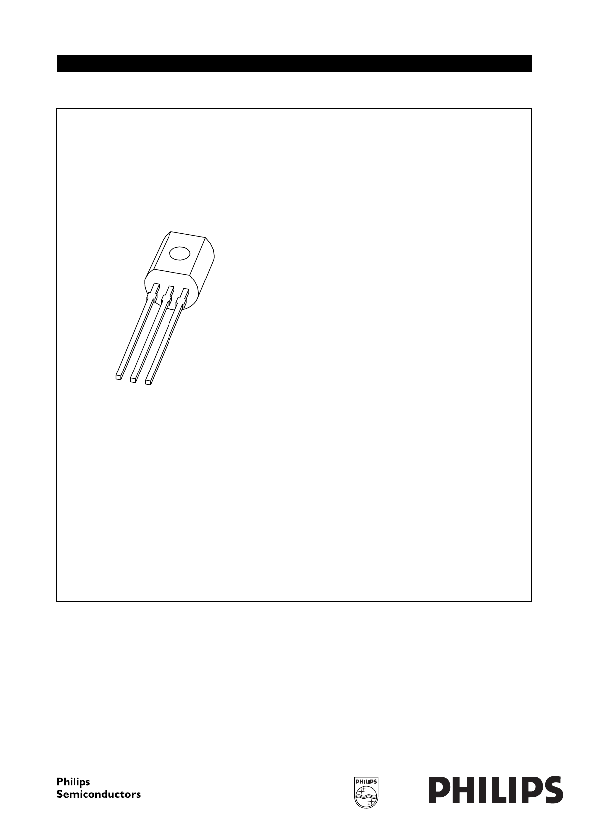
PNP transistor in a TO-92 (SOT54) plastic package.
handbook, halfpage
1
2
3
2
NPN complement: BC549.
MAM281
Fig.1 Simplified outline (TO-92; SOT54)
and symbol.
LIMITING VALUES
In accordance with the Absolute Maximum Rating System (IEC 134).
SYMBOL PARAMETER CONDITIONS MIN. MAX. UNIT
V
CBO
V
CEO
V
EBO
I
C
I
CM
I
BM
P
tot
T
stg
T
j
T
amb
collector-base voltage open emitter −−30 V
collector-emitter voltage open base −−30 V
emitter-base voltage open collector −−5V
collector current (DC) −−100 mA
peak collector current −−200 mA
peak base current −−200 mA
total power dissipation T
≤ 25 °C − 500 mW
amb
storage temperature −65 +150 °C
junction temperature − 150 °C
operating ambient temperature −65 +150 °C
3
1
1999 May 28 2
Philips Semiconductors Product specification
PNP general purpose transistor BC559
THERMAL CHARACTERISTICS
SYMBOL PARAMETER CONDITIONS VALUE UNIT
R
th j-a
Note
1. Transistor mounted on an FR4 printed-circuit board.
CHARACTERISTICS
=25°C unless otherwise specified.
T
j
SYMBOL PARAMETER CONDITIONS MIN. TYP. MAX. UNIT
I
CBO
I
EBO
h
FE
V
CEsat
V
BEsat
V
BE
C
c
f
T
F noise figure; BC559C I
thermal resistance from junction to ambient note 1 250 K/W
collector cut-off current IE= 0; VCB= −30 V −−1−15 nA
I
= 0; VCB= −30 V; Tj= 150 °C −−−4µA
E
emitter cut-off current IC= 0; VEB= −5V −−−100 nA
DC current gain; BC559C IC= −2 mA; VCE= −5 V; see Fig.2 420 − 800
collector-emitter saturation
voltage
IC= −10 mA; IB= −0.5 mA −−60 −300 mV
= −100 mA; IB= −5mA −−180 −650 mV
I
C
base-emitter saturation voltage IC= −10 mA; IB= −0.5 mA; note 1 −−750 − mV
I
= −100 mA; IB= −5 mA; note 1 −−930 − mV
C
base-emitter voltage IC= −2 mA; VCE= −5 V; note 2 −600 −650 −750 mV
I
= −10 mA; VCE= −5 V; note 2 −−−820 mV
C
collector capacitance IE=ie= 0; VCB= −10 V; f = 1 MHz − 4 − pF
transition frequency IE= −10 mA; VCB= −5 V; f = 100 MHz 100 −−MHz
= −200 µA; VCE= −5 V; RS=2kΩ;
C
−−4dB
f = 30 Hz to 15.7 kHz
=−200 µA; VCE= −5 V; RS=2kΩ;
I
C
−−4dB
f = 1 kHz; B = 200 Hz
Notes
1. V
decreases by about −1.7 mV/K with increasing temperature.
BEsat
2. VBE decreases by about −2 mV/K with increasing temperature.
1999 May 28 3
 Loading...