

Philips BC369G, BC369-16 Datasheet
DISCRETE SEMICONDUCTORS
DATA SH EET
ook, halfpage
M3D186
BC369
PNP medium power transistor
Product specification
Supersedes data of 1997 Feb 28
1999 Apr 26
Philips Semiconductors Product specification
PNP medium power transistor BC369
FEATURES
• High current (max. 1 A)
• Low voltage (max. 20 V).
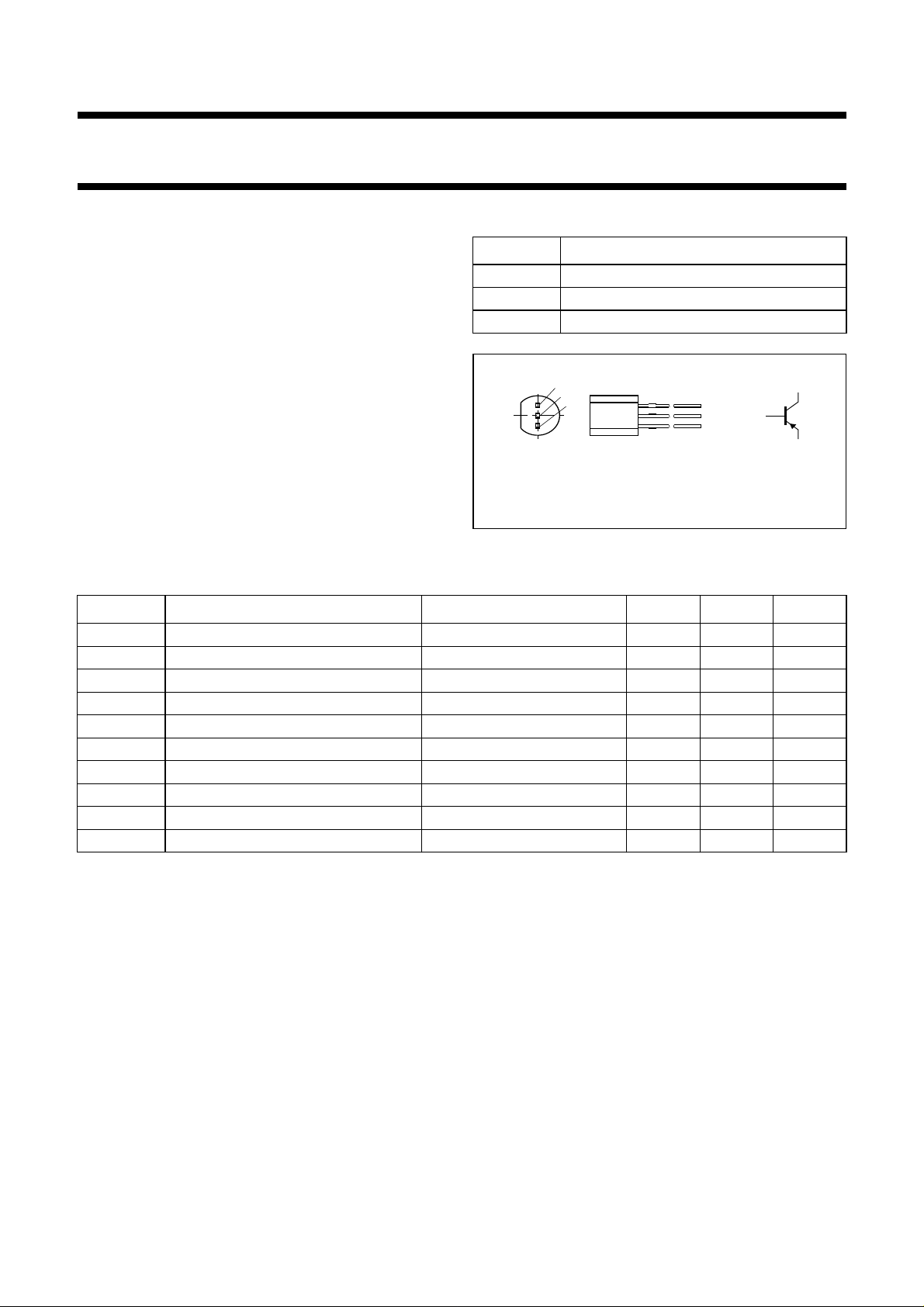
PINNING
PIN DESCRIPTION
1 base
2 collector
APPLICATIONS
3 emitter
• General purpose switching and amplification
• Power applications such as audio output stages.
handbook, halfpage
DESCRIPTION
NPN medium power transistor in a TO-92; SOT54 plastic
package. PNP complement: BC368.
1
2
3
1
MAM285
Fig.1 Simplified outline (TO-92; SOT54)
and symbol.
LIMITING VALUES
In accordance with the Absolute Maximum Rating System (IEC 134).
SYMBOL PARAMETER CONDITIONS MIN. MAX. UNIT
V
CBO
V
CEO
V
EBO
I
C
I
CM
I
BM
P
tot
T
stg
T
j
T
amb
collector-base voltage open emitter −−32 V
collector-emitter voltage open base −−20 V
emitter-base voltage open collector −−5V
collector current (DC) −−1A
peak collector current −−2A
peak base current −−200 mA
total power dissipation T
≤ 25 °C; note 1 − 0.83 W
amb
storage temperature −65 +150 °C
junction temperature − 150 °C
operating ambient temperature −65 +150 °C
2
3
Note
1. Transistor mounted on an FR4 printed-circuit board.
1999 Apr 26 2
Philips Semiconductors Product specification
PNP medium power transistor BC369
THERMAL CHARACTERISTICS
SYMBOL PARAMETER CONDITIONS VALUE UNIT
R
th j-a
Note
1. Transistor mounted on an FR4 printed-circuit board.
CHARACTERISTICS
=25°C unless otherwise specified.
T
j
SYMBOL PARAMETER CONDITIONS MIN. MAX. UNIT
I
CBO
I
EBO
h
FE
V
CEsat
V
BE
f
T
h
FE1
----------h
FE2
thermal resistance from junction to ambient note 1 150 K/W
collector cut-off current IE= 0; VCB= −25 V −−100 nA
I
= 0; VCB= −25 V; Tj= 150 °C −−10 µA
E
emitter cut-off current IC= 0; VEB= −5V −−100 nA
DC current gain IC= −5 mA; VCE= −10 V 50 −
I
= −500 mA; VCE= −1 V; see Fig.2 85 375
C
= −1 A; VCE= −1 V; see Fig.2 60 −
I
C
DC current gain I
= −500 mA; VCE= −1 V; see Fig.2
C
BC369-16 100 250
BC369-25 160 375
collector-emitter saturation voltage IC= −1 A; IB= −100 mA −−0.5 V
base-emitter voltage IC= −5 mA; VCE= −10 V −−0.7 V
I
= −1 A; VCE= −1V −−1V
C
transition frequency IC= −10 mA; VCE= −5 V; f = 100 MHz 40 − MHz
DC current gain ratio of the
I
= 500 mA; VCE =1V − 1.6
C
complementary pairs
1999 Apr 26 3
 Loading...