

Philips BC177 Datasheet
DISCRETE SEMICONDUCTORS
DATA SH EET
*
M3D125
BC177
PNP general purpose transistor
Product specification
Supersedes data of 1997 May 01
File under Discrete Semiconductors, SC04
1997 Jun 04
Philips Semiconductors Product specification
PNP general purpose transistor BC177
FEATURES
• Low current (max. 100 mA)
• Low voltage (max. 45 V).
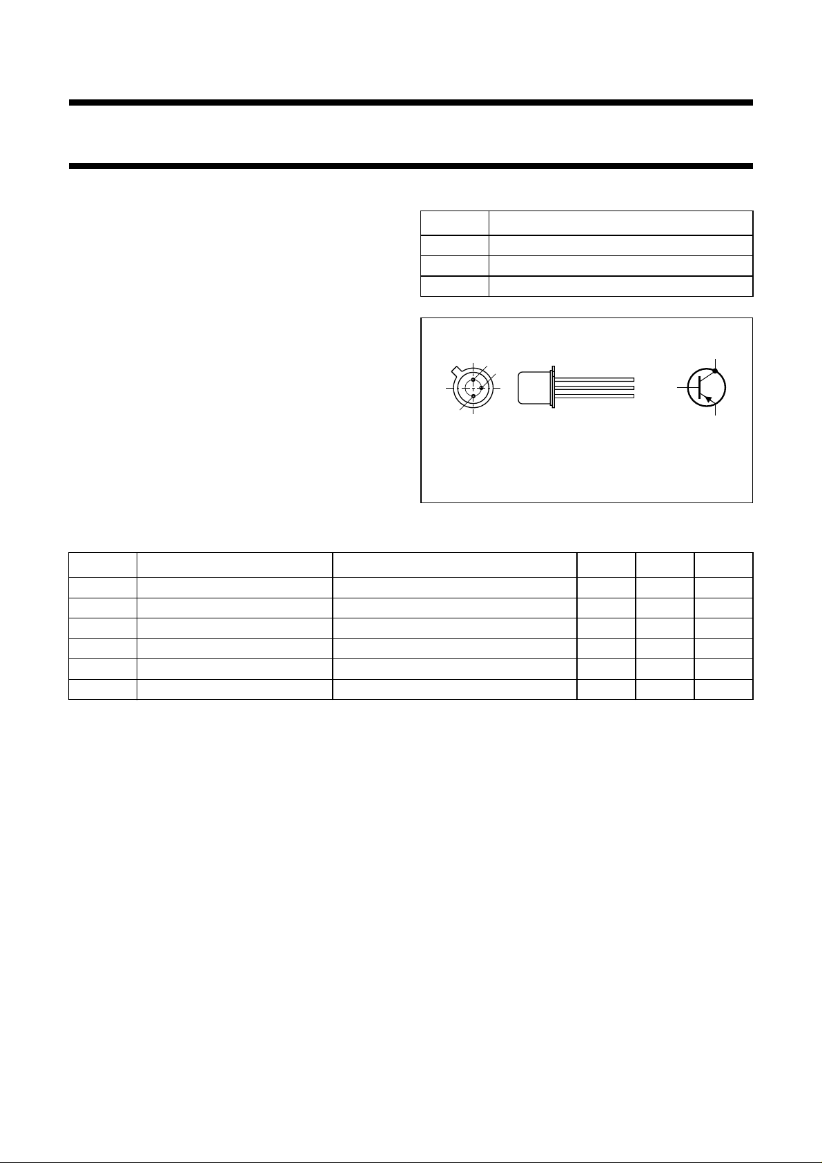
PINNING
PIN DESCRIPTION
1 emitter
2 base
APPLICATIONS
3 collector, connected to the case
• General purpose switching and amplification.
DESCRIPTION
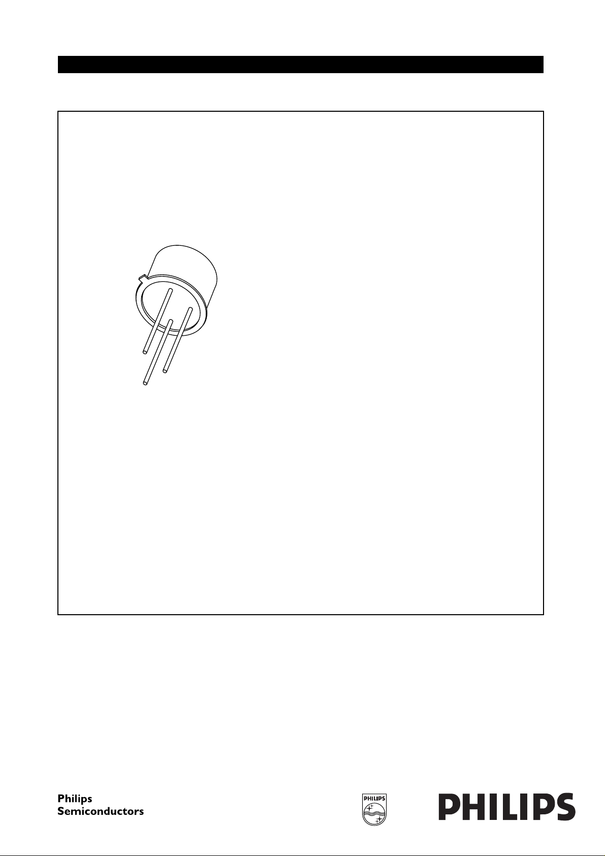
PNP transistor in a TO-18; SOT18 metal package.
NPN complement: BC107.
handbook, halfpage
3
1
2
2
MAM263
3
1
Fig.1 Simplified outline (TO-18; SOT18)
and symbol.
QUICK REFERENCE DATA
SYMBOL PARAMETER CONDITIONS MIN. MAX. UNIT
V
V
I
P
h
f
CBO
CEO
CM
tot
FE
T
collector-base voltage open emitter −−50 V
collector-emitter voltage open base −−45 V
peak collector current −−200 mA
total power dissipation T
≤ 25 °C − 300 mW
amb
DC current gain IC= −2 mA; VCE= −5 V 125 500
transition frequency IC= −10 mA; VCE= −5 V; f = 100 MHz 100 − MHz
1997 Jun 04 2

Philips Semiconductors Product specification
PNP general purpose transistor BC177
LIMITING VALUES
In accordance with the Absolute Maximum Rating System (IEC 134).
SYMBOL PARAMETER CONDITIONS MIN. MAX. UNIT
V
CBO
V
CEO
V
EBO
I
C
I
CM
I
BM
P
tot
T
stg
T
j
T
amb
collector-base voltage open emitter −−50 V
collector-emitter voltage open base −−45 V
emitter-base voltage open collector −−5V
collector current (DC) −−100 mA
peak collector current −−200 mA
peak base current −−200 mA
total power dissipation T
≤ 25 °C − 300 mW
amb
storage temperature −65 +150 °C
junction temperature − 175 °C
operating ambient temperature −65 +150 °C
THERMAL CHARACTERISTICS
SYMBOL PARAMETER CONDITIONS VALUE UNIT
R
R
th j-a
th j-c
thermal resistance from junction to ambient note 1 0.5 K/mW
thermal resistance from junction to case 0.2 K/mW
Note
1. Transistor mounted on an FR4 printed-circuit board.
1997 Jun 04 3
 Loading...