

Philips 74HC04, 74HCT04 Technical data
查询74HC04供应商
INTEGRATED CIRCUITS
DATA SH EET
74HC04; 74HCT04
Hex inverter
Product specification
Supersedes data of 1993 Sep 01
2003 Jul 23
Philips Semiconductors Product specification
Hex inverter 74HC04; 74HCT04
FEATURES
• Complies with JEDEC standard no. 8-1A
• ESD protection:
HBM EIA/JESD22-A114-A exceeds 2000 V
MM EIA/JESD22-A115-A exceeds 200 V.
• Specified from −40 to +85 °C and −40 to +125 °C.
DESCRIPTION
The 74HC/HCT04 are high-speed Si-gateCMOS devices
and are pin compatible with low power Schottky TTL
(LSTTL). They are specified in compliance with JEDEC
standard no. 7A. The 74HC/HCT04 provide six inverting
buffers.
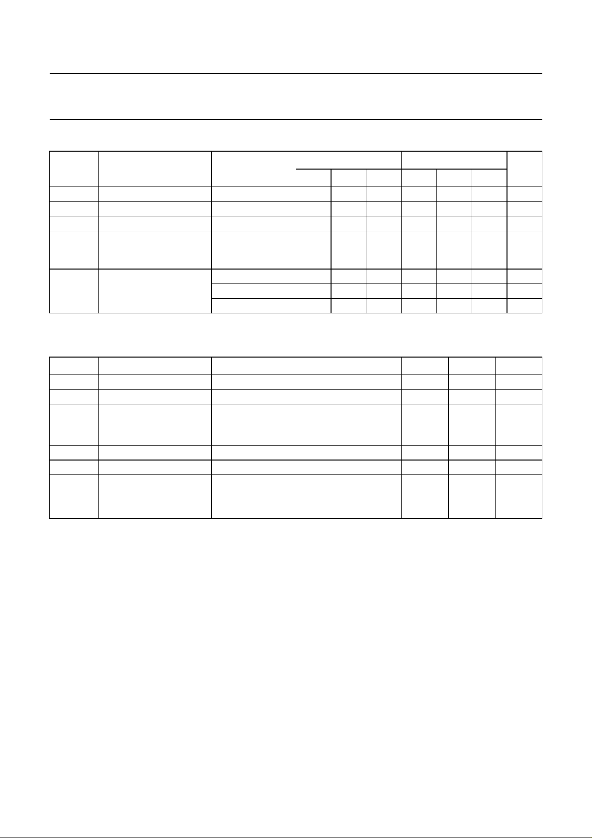
QUICK REFERENCE DATA
GND = 0 V; T
=25°C; tr=tf≤6.0 ns.
amb
SYMBOL PARAMETER CONDITIONS
t
PHL/tPLH
C
I
C
PD
propagation delay nA to nY CL= 15 pF; VCC=5V78ns
input capacitance 3.5 3.5 pF
power dissipation capacitance per gate notes 1 and 2 21 24 pF
Notes
1. C
is used to determine the dynamic power dissipation (PDin µW).
PD
PD=CPD× V
2
× fi× N+Σ(CL× V
CC
2
× fo) where:
CC
fi= input frequency in MHz;
fo= output frequency in MHz;
= output load capacitance in pF;
C
L
VCC= supply voltage in Volts;
N = total load switching outputs;
Σ(CL× V
2
× fo) = sum of the outputs.
CC
2. For 74HC04: the condition is VI= GND to VCC.
For 74HCT04: the condition is VI= GND to VCC− 1.5 V.
TYPICAL
UNIT
HC04 HCT04
FUNCTION TABLE
See note 1.
INPUT OUTPUT
nA nY
LH
HL
Note
1. H = HIGH voltage level;
L = LOW voltage level.
2003 Jul 23 2
Philips Semiconductors Product specification
Hex inverter 74HC04; 74HCT04
ORDERING INFORMATION
TYPE NUMBER
PACKAGE
TEMPERATURE RANGE PINS PACKAGE MATERIAL CODE
74HC04N −40 to +125 °C 14 DIP14 plastic SOT27-1
74HCT04N −40 to +125 °C 14 DIP14 plastic SOT27-1
74HC04D −40 to +125 °C 14 SO14 plastic SOT108-1
74HCT04D −40 to +125 °C 14 SO14 plastic SOT108-1
74HC04DB −40 to +125 °C 14 SSOP14 plastic SOT337-1
74HCT04DB −40 to +125 °C 14 SSOP14 plastic SOT337-1
74HC04PW −40 to +125 °C 14 TSSOP14 plastic SOT402-1
74HCT04PW −40 to +125 °C 14 TSSOP14 plastic SOT402-1
74HC04BQ −40 to +125 °C 14 DHVQFN14 plastic SOT762-1
74HCT04BQ −40 to +125 °C 14 DHVQFN14 plastic SOT762-1
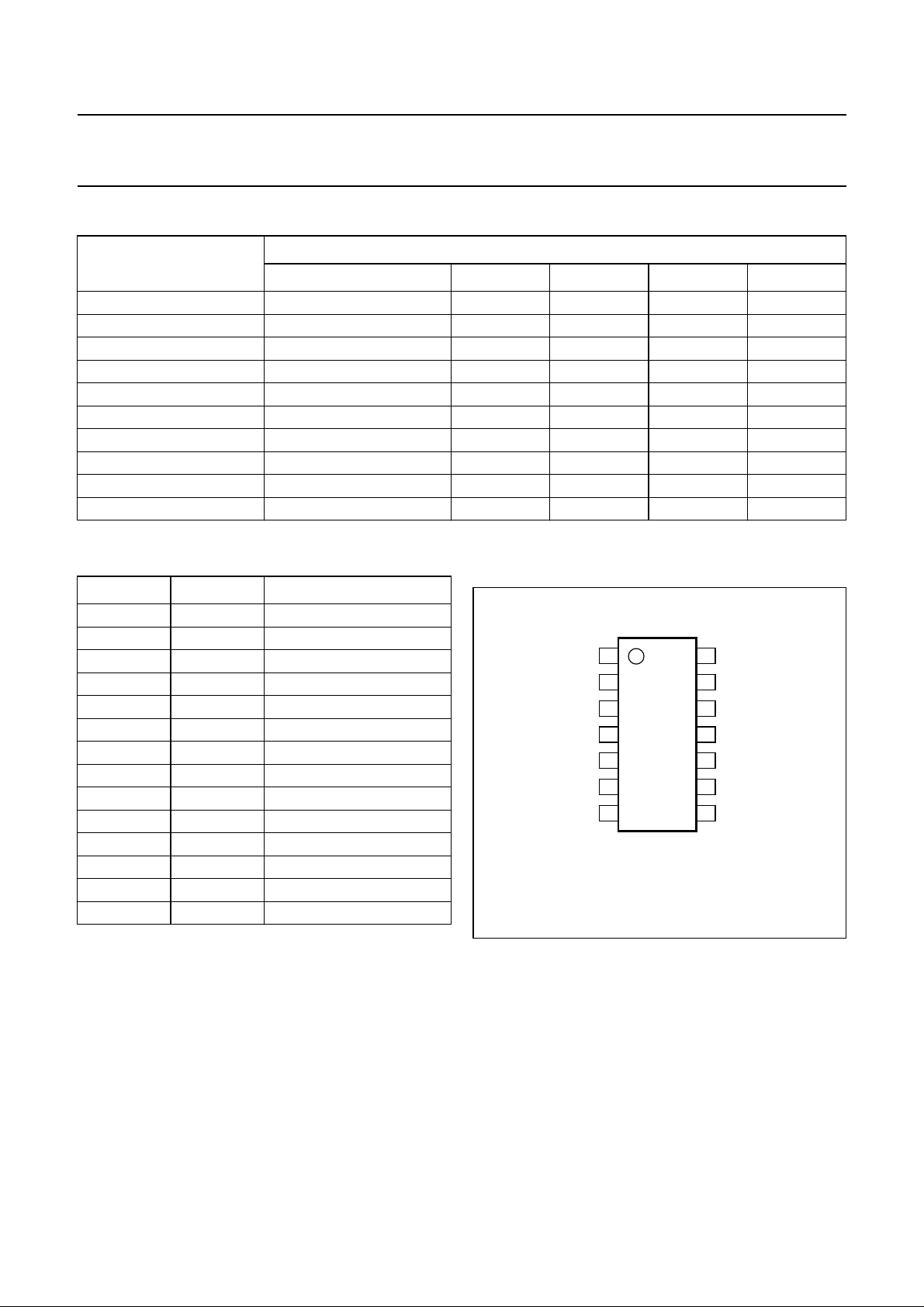
PINNING
PIN SYMBOL DESCRIPTION
1 1A data input
2 1Y data output
3 2A data input
4 2Y data output
5 3A data input
6 3Y data output
7 GND ground (0 V)
8 4Y data output
9 4A data input
10 5Y data output
11 5A data input
handbook, halfpage
1A
1Y
2A
2Y
3A
3Y
GND
1
2
3
4
04
5
6
7
MNA340
V
14
CC
13
6A
12
6Y
11
5A
10
5Y
9
4A
8
4Y
12 6Y data output
13 6A data input
14 V
CC
supply voltage
Fig.1 Pin configuration DIP14, SO14 and
(T)SSOP14.
2003 Jul 23 3
Philips Semiconductors Product specification
Hex inverter 74HC04; 74HCT04
V
handbook, halfpage
1Y
2A
2Y
3A
3Y
2
3
4
5
6
Top view
1A
CC
114
(1)
GND
8
7
GND
4Y
13
12
11
10
9
MBL760
6A
6Y
5A
5Y
4A
handbook, halfpage
1Y
2Y
3Y
4Y
5Y
6Y
2
4
6
8
10
12
1A
1
2A
3
3A
5
4A
9
5A
11
6A
13
(1) The die substrate is attached to this pad using conductive die
attach material. It can not be used as a supply pin or input.
Fig.2 Pin configuration DHVQFN14.
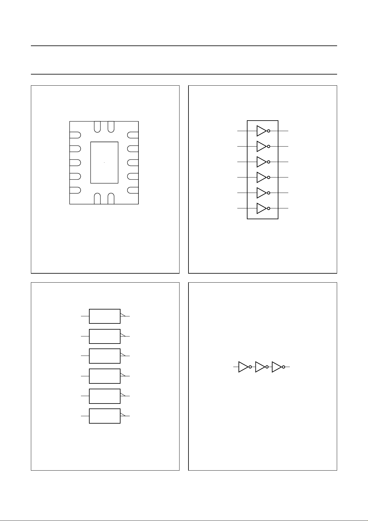
handbook, halfpage
1
3
5
9
11
1
1
1
1
1
2
4
6
8
10
handbook, halfpage
MNA342
Fig.3 Logic symbol.
A
Y
MNA341
13
1
MNA343
12
Fig.4 IEC logic symbol. Fig.5 Logic diagram (one inverter).
2003 Jul 23 4
Philips Semiconductors Product specification
Hex inverter 74HC04; 74HCT04
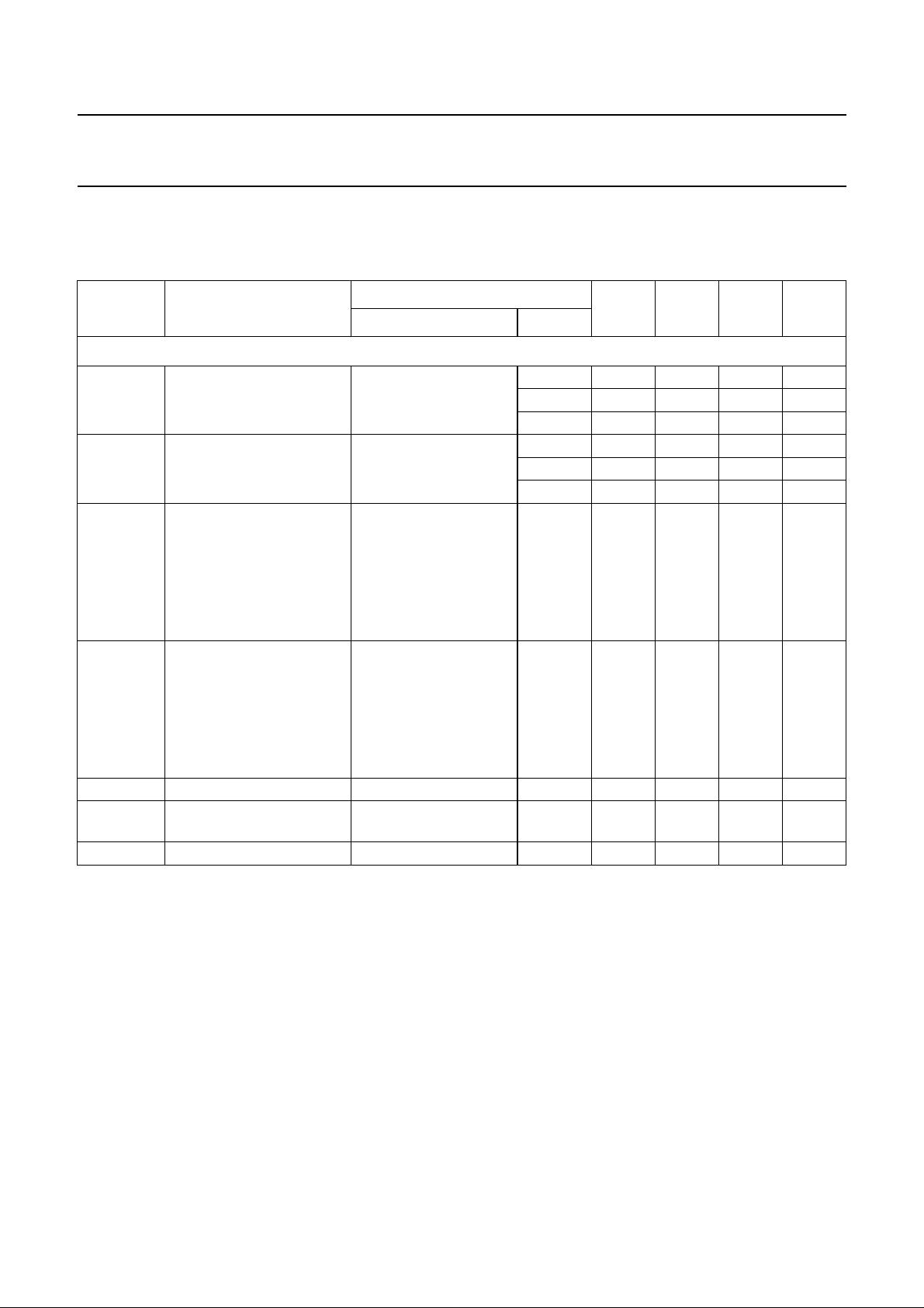
RECOMMENDED OPERATING CONDITIONS
SYMBOL PARAMETER CONDITIONS
UNIT
MIN. TYP. MAX. MIN. TYP. MAX.
74HC04 74HCT04
V
CC
V
I
V
O
T
amb
supply voltage 2.0 5.0 6.0 4.5 5.0 5.5 V
input voltage 0 − V
output voltage 0 − V
ambient temperature see DC and AC
−40 +25 +125 −40 +25 +125 °C
0 − V
CC
0 − V
CC
CC
CC
V
V
characteristicsper
device
t
, t
r
f
input rise and fall times VCC= 2.0 V −−1000 −−−ns
= 4.5 V − 6.0 500 − 6.0 500 ns
V
CC
V
= 6.0 V −−400 −−−ns
CC
LIMITING VALUES
In accordance with the Absolute Maximum Rating System (IEC 60134); voltages are referenced to GND (ground = 0 V).
SYMBOL PARAMETER CONDITIONS MIN. MAX. UNIT
V
CC
I
IK
I
OK
I
O
supply voltage −0.5 +7.0 V
input diode current VI< −0.5 V or VI>VCC+ 0.5 V −±20 mA
output diode current VO< −0.5 V or VO>VCC+ 0.5 V −±20 mA
output source or sink
−0.5V<VO<VCC+ 0.5 V −±25 mA
current
I
, I
CC
T
stg
P
tot
GNDVCC
or GND current −±50 mA
storage temperature −65 +150 °C
power dissipation
DIP14 package T
other packages T
= −40 to +125 °C; note 1 − 750 mW
amb
= −40 to +125 °C; note 2 − 500 mW
amb
Notes
1. For DIP14 packages: above 70 °C derate linearly with 12 mW/K.
2. For SO14 packages: above 70 °C derate linearly with 8 mW/K.
For SSOP14 and TSSOP14 packages: above 60 °C derate linearly with 5.5 mW/K.
For DHVQFN14 packages: above 60 °C derate linearly with 4.5 mW/K.
2003 Jul 23 5
Philips Semiconductors Product specification
Hex inverter 74HC04; 74HCT04
DC CHARACTERISTICS
Type 74HC04
At recommended operating conditions; voltages are referenced to GND (ground=0V).
SYMBOL PARAMETER
T
=25°C
amb
V
V
V
V
I
I
I
IH
IL
OH
OL
LI
OZ
CC
HIGH-level input voltage 2.0 1.5 1.2 − V
LOW-level input voltage 2.0 − 0.8 0.5 V
HIGH-level output voltage VI=VIHor V
LOW-level output voltage VI=VIHor V
input leakage current VI=VCCor GND 6.0 − 0.1 ±0.1 µA
3-state output OFF current VI=VIHor VIL;
quiescent supply current VI=VCCor GND; IO= 0 6.0 −−2µA
TEST CONDITIONS
MIN. TYP. MAX. UNIT
OTHER V
CC
(V)
4.5 3.15 2.4 − V
6.0 4.2 3.2 − V
4.5 − 2.1 1.35 V
6.0 − 2.8 1.8 V
IL
IO= −20 µA 2.0 1.9 2.0 − V
I
= −20 µA 4.5 4.4 4.5 − V
O
I
= −4.0 mA 4.5 3.98 4.32 − V
O
I
= −20 µA 6.0 5.9 6.0 − V
O
I
= −5.2 mA 6.0 5.48 5.81 − V
O
IL
IO=20µA 2.0 − 0 0.1 V
I
=20µA 4.5 − 0 0.1 V
O
I
= 4.0 mA 4.5 − 0.15 0.26 V
O
I
=20µA 6.0 − 0 0.1 V
O
I
= 5.2 mA 6.0 − 0.16 0.26 V
O
6.0 −−±.0.5 µA
VO=VCCor GND
2003 Jul 23 6
 Loading...