

Page 1
Color Television Chassis
18970_000_100325.eps
100325
LC9.3L
LA
Contents Page Contents Page
1. Revision List 2
2. Technical Specifications and Connections 2
3. Precautions, Notes, and Abbreviation List 5
4. Mechanical Instructions 9
5. Service Modes, Error Codes, and Fault Finding 17
6. Alignments 24
7. Circuit Descriptions 29
8. IC Data Sheets 36
9. Block Diagrams
Wiring Diagram 32" - 40" (Picasso) 39
Wiring Diagram 32" - 46" (van Gogh) 40
Wiring Diagram 32" 46" (Da Vinci) 41
Block Diagram Video 42
Block Diagram Audio 43
Block Diagram Control & Clock Signals 44
Block Diagram I2C 45
Supply Lines Overview 46
10. Circuit Diagrams and PWB Layouts Drawing PWB
Ambilight: Everlight LED Common 1
Ambilight: Everlight LED Common 2 (AL1B) 48 54
Ambilight: 3 LED Everlight (AL2A) 49 54
Ambilight: 9 LED Everlight (AL2A) 50 54
Ambilight: 9 LED Everlight (AL2B) 51 54
Ambilight: 15 LED Everlight (AL2A) 52 54
Ambilight: 15 LED Everlight (AL2B) 53 54
SSB: DC-DC (B01A) 55 75-76
SSB: TUNER & Analog Demodulator (B02) 56 75-76
SSB: CLASS-D & Muting (B03) 57 75-76
SSB: MTK Power (B04A) 58 75-76
SSB: GDDR3 (B04B) 59 75-76
SSB: Flash, EJTAG & Display Interface (B04C) 60 75-76
SSB: Ambilight Microcontroller (B05) 61 75-76
SSB: HDMI & Multiplexer (B06) 62 75-76
(AL1A) 47 54
SSB: Analog I/O - Audio (B07B) 63 75-76
SSB: Analog I/O - YPbPr & Cinch (B07C) 64 75-76
SSB: USB (B07D) 65 75-76
SSB: VGA (B07E) 66 75-76
SSB: Hospitality (B08) 67 75-76
SSB: Ambilight CPLD (B13) 68 75-76
SSB: TCON Control (B14A) 69 75-76
SSB: TCON DC/DC (B14B) 70 75-76
SSB: P Gamma & VCOM & Flash (B14C) 71 75-76
SSB: MPD (B14D) 72 75-76
SSB: Mini LVDS (B14E) 73 75-76
SSB: Connectors (B14F) 74 75-76
SSB: SRP List Explanation 77
SSB: SRP List 78
IR/LED Board (J) 79 80
Keyboard Control Board (E) 81 82
11. Styling Sheets
Styling Sheet 32" - 40" (Picasso) 83
Styling Sheet 32" - 46" (van Gogh) 84
Styling Sheet 32" - 46" (Da Vinci) 85
©
Copyright 2010 Koninklijke Philips Electronics N.V.
All rights reserved. No part of this publication may be reproduced, stored in a
retrieval system or transmitted, in any form or by any means, electronic, mechanical,
photocopying, or otherwise without the prior permission of Philips.
Published by ER/JY 1063 BU TV Consumer Care Printed in the Netherlands Subject to modification EN 3122 785 18970
2010-Mar-26
Page 2
EN 2 LC9.3L LA1.
Revision List
1. Revision List
Manual xxxx xxx xxxx.0
• First release.
2. Technical Specifications and Connections
Index of this chapter:
2.1 Technical Specifications
2.2 Directions for Use
2.3 Connections
2.4 Chassis Overview
Notes:
• Figures can deviate due to the different set executions.
• Specifications are indicative (subject to change).
2.1 Technical Specifications
For on-line product support please use the links in Table 2-1.
Here is product information available, as well as getting started,
user manuals, frequently asked questions and software &
drivers.
Table 2-1 Described Model numbers
CTN Styling Published in:
32PFL3805D/78
32PFL5605D/78
32PFL6605D/78
40PFL3805D/78
40PFL5605D/78
40PFL6605D/78
46PFL5605D/78
46PFL6605D/78
Picasso 3122 785 18970
van Gogh 3122 785 18970
da Vinci 3122 785 18970
Picasso 3122 785 18970
van Gogh 3122 785 18970
da Vinci 3122 785 18970
van Gogh 3122 785 18970
da Vinci 3122 785 18970
2.2 Directions for Use
You can download this information from the following websites:
http://www.philips.com/support
http://www.p4c.philips.com
2010-Mar-26
Page 3
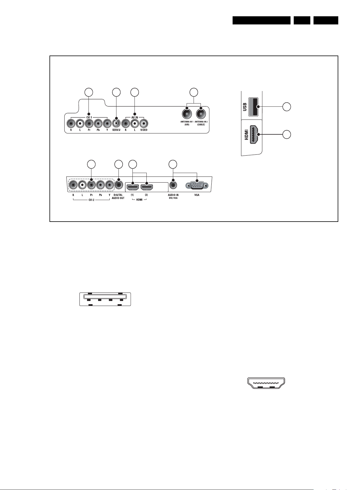
2.3 Connections
18920_001_100317.eps
100317
Side connectors
Back connectors
Bottom connectors
1
2
345 6
789 10
1 2 3 4
10000_022_090121.eps
090121
10000_017_090121.eps
090428
19
1
18 2
Technical Specifications and Connections
EN 3LC9.3L LA 2.
Note: The following connector color abbreviations are used
(according to DIN/IEC 757): Bk= Black, Bu= Blue, Gn= Green,
Gy= Grey, Rd= Red, Wh= White, Ye= Yellow.
2.3.1 Side Connectors
1 - USB2.0
Figure 2-2 USB (type A)
1-+5V k
2 -Data (-) jk
3 -Data (+) jk
4 -Ground Gnd H
2 - HDMI: Digital Video, Digital Audio - In (see HDMI 1 & 2)
2.3.2 Rear Connectors
3 - CVI-1: Cinch: Video YPbPr - In, Audio - In
Gn - Video Y 1 V
Bu - Video Pb 0.7 V
Rd - Video Pr 0.7 V
Wh - Audio - L 0.5 V
Rd - Audio - R 0.5 V
4 - Service Connector (UART)
1 -Ground Gnd H
2 -UART_TX Transmit k
3 -UART_RX Receive j
Figure 2-1 Connection overview
/ 75 Ω jq
PP
/ 75 Ω jq
PP
/ 75 Ω jq
PP
/ 10 kΩ jq
RMS
/ 10 kΩ jq
RMS
5 - Cinch: AV IN: Video CVBS - In, Audio - In
Ye - Video CVBS 1 V
Wh - Audio L 0.5 V
Rd - Audio R 0.5 V
6 - Aerial - In (Air and Cable)
- - F-type Coax, 75 Ω D
2.3.3 Bottom Connectors
7 - CVI-2: Cinch: Video YPbPr - In, Audio - In
Gn - Video Y 1 V
Bu - Video Pb 0.7 V
Rd - Video Pr 0.7 V
Wh - Audio - L 0.5 V
Rd - Audio - R 0.5 V
8 - Cinch: S/PDIF - Out
Bk - Coaxial 0.4 - 0.6V
PP
PP
9 - HDMI 1 and 2: Digital Video, Digital Audio - In
Figure 2-3 HDMI (type A) connector
1 -D2+ Data channel j
2 -Shield Gnd H
3 -D2- Data channel j
4 -D1+ Data channel j
5 -Shield Gnd H
6 -D1- Data channel j
7 -D0+ Data channel j
8 -Shield Gnd H
9 -D0- Data channel j
/ 75 ohm jq
/ 10 kohm jq
RMS
/ 10 kohm jq
RMS
/ 75 Ω jq
/ 75 Ω jq
PP
/ 75 Ω jq
PP
/ 10 kΩ jq
RMS
/ 10 kΩ jq
RMS
/ 75 ohm kq
PP
2010-Mar-26
Page 4

EN 4 LC9.3L LA2.
1
6
10
11
5
15
10000_002_090121.eps
090127
Technical Specifications and Connections
10 - CLK+ Data channel j
11 - Shield Gnd H
12 - CLK- Data channel j
13 - Easylink/CEC Control channel jk
14 - n.c.
15 - DDC_SCL DDC clock j
16 - DDC_SDA DDC data jk
17 - Ground Gnd H
18 - +5V j
19 - HPD Hot Plug Detect j
20 - Ground Gnd H
10 - Mini Jack: DVI/VGA: Audio - In
Bk - Audio 0.5 V
/ 10 kΩ jo
RMS
10 - VGA: Video RGB - In
Figure 2-4 VGA Connector
2.4 Chassis Overview
Refer to chapter 9. Block Diagrams for PWB/CBA locations.
1 -Video Red 0.7 V
2 -Video Green 0.7 V
3 -Video Blue 0.7 V
4-n.c.
/ 75 Ω j
PP
/ 75 Ω j
PP
/ 75 Ω j
PP
5 -Ground Gnd H
6 -Ground Red Gnd H
7 -Ground Green Gnd H
8 -Ground Blue Gnd H
9-+5V
10 - Ground Sync Gnd H
+5 V j
DC
11 - n.c.
12 - DDC_SDA DDC data j
13 - H-sync 0 - 5 V j
14 - V-sync 0 - 5 V j
15 - DDC_SCL DDC clock j
2010-Mar-26
Page 5

Precautions, Notes, and Abbreviation List
3. Precautions, Notes, and Abbreviation List
EN 5LC9.3L LA 3.
Index of this chapter:
3.1 Safety Instructions
3.2 Warnings
3.3 Notes
3.4 Abbreviation List
3.1 Safety Instructions
Safety regulations require the following during a repair:
• Connect the set to the Mains/AC Power via an isolation
transformer (> 800 VA).
• Replace safety components, indicated by the symbol h,
only by components identical to the original ones. Any
other component substitution (other than original type) may
increase risk of fire or electrical shock hazard. Of de set
ontploft!
Safety regulations require that after a repair, the set must be
returned in its original condition. Pay in particular attention to
the following points:
• Route the wire trees correctly and fix them with the
mounted cable clamps.
• Check the insulation of the Mains/AC Power lead for
external damage.
• Check the strain relief of the Mains/AC Power cord for
proper function.
• Check the electrical DC resistance between the Mains/AC
Power plug and the secondary side (only for sets that have
a Mains/AC Power isolated power supply):
1. Unplug the Mains/AC Power cord and connect a wire
between the two pins of the Mains/AC Power plug.
2. Set the Mains/AC Power switch to the “on” position
(keep the Mains/AC Power cord unplugged!).
3. Measure the resistance value between the pins of the
Mains/AC Power plug and the metal shielding of the
tuner or the aerial connection on the set. The reading
should be between 4.5 MΩ and 12 MΩ.
4. Switch “off” the set, and remove the wire between the
two pins of the Mains/AC Power plug.
• Check the cabinet for defects, to prevent touching of any
inner parts by the customer.
picture carrier at 475.25 MHz for PAL, or 61.25 MHz for
NTSC (channel 3).
• Where necessary, measure the waveforms and voltages
with (D) and without (E) aerial signal. Measure the
voltages in the power supply section both in normal
operation (G) and in stand-by (F). These values are
indicated by means of the appropriate symbols.
3.3.2 Schematic Notes
• All resistor values are in ohms, and the value multiplier is
often used to indicate the decimal point location (e.g. 2K2
indicates 2.2 kΩ).
• Resistor values with no multiplier may be indicated with
either an “E” or an “R” (e.g. 220E or 220R indicates 220 Ω).
• All capacitor values are given in micro-farads (μ=× 10
nano-farads (n =× 10
• Capacitor values may also use the value multiplier as the
decimal point indication (e.g. 2p2 indicates 2.2 pF).
• An “asterisk” (*) indicates component usage varies. Refer
to the diversity tables for the correct values.
• The correct component values are listed on the Philips
Spare Parts Web Portal.
3.3.3 Spare Parts
For the latest spare part overview, consult your Philips Spare
Part web portal.
3.3.4 BGA (Ball Grid Array) ICs
Introduction
For more information on how to handle BGA devices, visit this
URL: http://www.atyourservice-magazine.com
“Magazine”, then go to “Repair downloads”. Here you will find
Information on how to deal with BGA-ICs.
BGA Temperature Profiles
For BGA-ICs, you must use the correct temperature-profile.
Where applicable and available, this profile is added to the IC
Data Sheet information section in this manual.
-9
), or pico-farads (p =× 10
. Select
-12
-6
),
).
3.2 Warnings
• All ICs and many other semiconductors are susceptible to
electrostatic discharges (ESD w). Careless handling
during repair can reduce life drastically. Make sure that,
during repair, you are connected with the same potential as
the mass of the set by a wristband with resistance. Keep
components and tools also at this same potential.
• Be careful during measurements in the high voltage
section.
• Never replace modules or other components while the unit
is switched “on”.
• When you align the set, use plastic rather than metal tools.
This will prevent any short circuits and the danger of a
circuit becoming unstable.
3.3 Notes
3.3.1 General
• Measure the voltages and waveforms with regard to the
chassis (= tuner) ground (H), or hot ground (I), depending
on the tested area of circuitry. The voltages and waveforms
shown in the diagrams are indicative. Measure them in the
Service Default Mode with a colour bar signal and stereo
sound (L: 3 kHz, R: 1 kHz unless stated otherwise) and
3.3.5 Lead-free Soldering
Due to lead-free technology some rules have to be respected
by the workshop during a repair:
• Use only lead-free soldering tin. If lead-free solder paste is
required, please contact the manufacturer of your soldering
equipment. In general, use of solder paste within
workshops should be avoided because paste is not easy to
store and to handle.
• Use only adequate solder tools applicable for lead-free
soldering tin. The solder tool must be able:
– To reach a solder-tip temperature of at least 400°C.
– To stabilize the adjusted temperature at the solder-tip.
– To exchange solder-tips for different applications.
• Adjust your solder tool so that a temperature of around
360°C - 380°C is reached and stabilized at the solder joint.
Heating time of the solder-joint should not exceed ~ 4 sec.
Avoid temperatures above 400°C, otherwise wear-out of
tips will increase drastically and flux-fluid will be destroyed.
To avoid wear-out of tips, switch “off” unused equipment or
reduce heat.
• Mix of lead-free soldering tin/parts with leaded soldering
tin/parts is possible but PHILIPS recommends strongly to
avoid mixed regimes. If this cannot be avoided, carefully
clear the solder-joint from old tin and re-solder with new tin.
2010-Mar-26
Page 6
EN 6 LC9.3L LA3.
Precautions, Notes, and Abbreviation List
3.3.6 Alternative BOM identification
It should be noted that on the European Service website,
“Alternative BOM” is referred to as “Design variant”.
The third digit in the serial number (example:
AG2B0335000001) indicates the number of the alternative
B.O.M. (Bill Of Materials) that has been used for producing the
specific TV set. In general, it is possible that the same TV
model on the market is produced with e.g. two different types
of displays, coming from two different suppliers. This will then
result in sets which have the same CTN (Commercial Type
Number; e.g. 28PW9515/12) but which have a different B.O.M.
number.
By looking at the third digit of the serial number, one can
identify which B.O.M. is used for the TV set he is working with.
If the third digit of the serial number contains the number “1”
(example: AG1B033500001), then the TV set has been
manufactured according to B.O.M. number 1. If the third digit is
a “2” (example: AG2B0335000001), then the set has been
produced according to B.O.M. no. 2. This is important for
ordering the correct spare parts!
For the third digit, the numbers 1...9 and the characters A...Z
can be used, so in total: 9 plus 26= 35 different B.O.M.s can be
indicated by the third digit of the serial number.
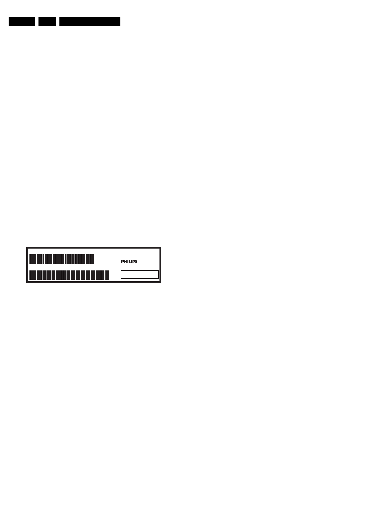
Identification: The bottom line of a type plate gives a 14-digit
serial number. Digits 1 and 2 refer to the production centre (e.g.
AG is Bruges), digit 3 refers to the B.O.M. code, digit 4 refers
to the Service version change code, digits 5 and 6 refer to the
production year, and digits 7 and 8 refer to production week (in
example below it is 2006 week 17). The 6 last digits contain the
serial number.
MODEL :
PROD.NO:
32PF9968/10
AG 1A0617 000001
MADE IN BELGIUM
220-240V 50/60Hz
VHF+S+H+UHF
S
10000_024_090121.eps
~
BJ3.0E LA
Figure 3-1 Serial number (example)
3.3.7 Board Level Repair (BLR) or Component Level Repair (CLR)
If a board is defective, consult your repair procedure to decide
if the board has to be exchanged or if it should be repaired on
component level.
If your repair procedure says the board should be exchanged
completely, do not solder on the defective board. Otherwise, it
cannot be returned to the O.E.M. supplier for back charging!
3.3.8 Practical Service Precautions
• It makes sense to avoid exposure to electrical shock.
While some sources are expected to have a possible
dangerous impact, others of quite high potential are of
limited current and are sometimes held in less regard.
• Always respect voltages. While some may not be
dangerous in themselves, they can cause unexpected
reactions that are best avoided. Before reaching into a
powered TV set, it is best to test the high voltage insulation.
It is easy to do, and is a good service precaution.
128W
100105
3.4 Abbreviation List
0/6/12 SCART switch control signal on A/V
board. 0 = loop through (AUX to TV),
6 = play 16 : 9 format, 12 = play 4 : 3
format
AARA Automatic Aspect Ratio Adaptation:
algorithm that adapts aspect ratio to
remove horizontal black bars; keeps
the original aspect ratio
ACI Automatic Channel Installation:
algorithm that installs TV channels
directly from a cable network by
means of a predefined TXT page
ADC Analogue to Digital Converter
AFC Automatic Frequency Control: control
signal used to tune to the correct
frequency
AGC Automatic Gain Control: algorithm that
controls the video input of the feature
box
AM Amplitude Modulation
AP Asia Pacific
AR Aspect Ratio: 4 by 3 or 16 by 9
ASF Auto Screen Fit: algorithm that adapts
aspect ratio to remove horizontal black
bars without discarding video
information
ATSC Advanced Television Systems
Committee, the digital TV standard in
the USA
ATV See Auto TV
Auto TV A hardware and software control
system that measures picture content,
and adapts image parameters in a
dynamic way
AV External Audio Video
AVC Audio Video Controller
AVIP Audio Video Input Processor
B/G Monochrome TV system. Sound
carrier distance is 5.5 MHz
BDS Business Display Solutions (iTV)
BLR Board-Level Repair
BTSC Broadcast Television Standard
Committee. Multiplex FM stereo sound
system, originating from the USA and
used e.g. in LATAM and AP-NTSC
countries
B-TXT Blue TeleteXT
C Centre channel (audio)
CEC Consumer Electronics Control bus:
remote control bus on HDMI
connections
CL Constant Level: audio output to
connect with an external amplifier
CLR Component Level Repair
ComPair Computer aided rePair
CP Connected Planet / Copy Protection
CSM Customer Service Mode
CTI Color Transient Improvement:
manipulates steepness of chroma
transients
CVBS Composite Video Blanking and
Synchronization
DAC Digital to Analogue Converter
DBE Dynamic Bass Enhancement: extra
low frequency amplification
DCM Data Communication Module. Also
referred to as System Card or
Smartcard (for iTV).
DDC See “E-DDC”
D/K Monochrome TV system. Sound
carrier distance is 6.5 MHz
DFI Dynamic Frame Insertion
2010-Mar-26
Page 7

Precautions, Notes, and Abbreviation List
EN 7LC9.3L LA 3.
DFU Directions For Use: owner's manual
DMR Digital Media Reader: card reader
DMSD Digital Multi Standard Decoding
DNM Digital Natural Motion
DNR Digital Noise Reduction: noise
reduction feature of the set
DRAM Dynamic RAM
DRM Digital Rights Management
DSP Digital Signal Processing
DST Dealer Service Tool: special remote
control designed for service
technicians
DTCP Digital Transmission Content
Protection; A protocol for protecting
digital audio/video content that is
traversing a high speed serial bus,
such as IEEE-1394
DVB-C Digital Video Broadcast - Cable
DVB-T Digital Video Broadcast - Terrestrial
DVD Digital Versatile Disc
DVI(-d) Digital Visual Interface (d= digital only)
E-DDC Enhanced Display Data Channel
(VESA standard for communication
channel and display). Using E-DDC,
the video source can read the EDID
information form the display.
EDID Extended Display Identification Data
(VESA standard)
EEPROM Electrically Erasable and
Programmable Read Only Memory
EMI Electro Magnetic Interference
EPG Electronic Program Guide
EPLD Erasable Programmable Logic Device
EU Europe
EXT EXTernal (source), entering the set by
SCART or by cinches (jacks)
FDS Full Dual Screen (same as FDW)
FDW Full Dual Window (same as FDS)
FLASH FLASH memory
FM Field Memory or Frequency
Modulation
FPGA Field-Programmable Gate Array
FTV Flat TeleVision
Gb/s Giga bits per second
G-TXT Green TeleteXT
H H_sync to the module
HD High Definition
HDD Hard Disk Drive
HDCP High-bandwidth Digital Content
Protection: A “key” encoded into the
HDMI/DVI signal that prevents video
data piracy. If a source is HDCP coded
and connected via HDMI/DVI without
the proper HDCP decoding, the
picture is put into a “snow vision” mode
or changed to a low resolution. For
normal content distribution the source
and the display device must be
enabled for HDCP “software key”
decoding.
HDMI High Definition Multimedia Interface
HP HeadPhone
I Monochrome TV system. Sound
2
I
C Inter IC bus
2
I
D Inter IC Data bus
2
I
S Inter IC Sound bus
carrier distance is 6.0 MHz
IF Intermediate Frequency
IR Infra Red
IRQ Interrupt Request
ITU-656 The ITU Radio communication Sector
(ITU-R) is a standards body
subcommittee of the International
Telecommunication Union relating to
radio communication. ITU-656 (a.k.a.
SDI), is a digitized video format used
for broadcast grade video.
Uncompressed digital component or
digital composite signals can be used.
The SDI signal is self-synchronizing,
uses 8 bit or 10 bit data words, and has
a maximum data rate of 270 Mbit/s,
with a minimum bandwidth of 135
MHz.
ITV Institutional TeleVision; TV sets for
hotels, hospitals etc.
LS Last Status; The settings last chosen
by the customer and read and stored
in RAM or in the NVM. They are called
at start-up of the set to configure it
according to the customer's
preferences
LATAM Latin America
LCD Liquid Crystal Display
LED Light Emitting Diode
L/L' Monochrome TV system. Sound
carrier distance is 6.5 MHz. L' is Band
I, L is all bands except for Band I
LPL LG.Philips LCD (supplier)
LS Loudspeaker
LVDS Low Voltage Differential Signalling
Mbps Mega bits per second
M/N Monochrome TV system. Sound
carrier distance is 4.5 MHz
MHEG Part of a set of international standards
related to the presentation of
multimedia information, standardised
by the Multimedia and Hypermedia
Experts Group. It is commonly used as
a language to describe interactive
television services
MIPS Microprocessor without Interlocked
Pipeline-Stages; A RISC-based
microprocessor
MOP Matrix Output Processor
MOSFET Metal Oxide Silicon Field Effect
Transistor, switching device
MPEG Motion Pictures Experts Group
MPIF Multi Platform InterFace
MUTE MUTE Line
MTV Mainstream TV: TV-mode with
Consumer TV features enabled (iTV)
NC Not Connected
NICAM Near Instantaneous Compounded
Audio Multiplexing. This is a digital
sound system, mainly used in Europe.
NTC Negative Temperature Coefficient,
non-linear resistor
NTSC National Television Standard
Committee. Color system mainly used
in North America and Japan. Color
carrier NTSC M/N= 3.579545 MHz,
NTSC 4.43= 4.433619 MHz (this is a
VCR norm, it is not transmitted off-air)
NVM Non-Volatile Memory: IC containing
TV related data such as alignments
O/C Open Circuit
OSD On Screen Display
OAD Over the Air Download. Method of
software upgrade via RF transmission.
Upgrade software is broadcasted in
TS with TV channels.
OTC On screen display Teletext and
Control; also called Artistic (SAA5800)
P50 Project 50: communication protocol
between TV and peripherals
PAL Phase Alternating Line. Color system
mainly used in West Europe (color
carrier= 4.433619 MHz) and South
America (color carrier PAL M=
2010-Mar-26
Page 8

EN 8 LC9.3L LA3.
Precautions, Notes, and Abbreviation List
3.575612 MHz and PAL N= 3.582056
MHz)
PCB Printed Circuit Board (same as “PWB”)
PCM Pulse Code Modulation
PDP Plasma Display Panel
PFC Power Factor Corrector (or Pre-
conditioner)
PIP Picture In Picture
PLL Phase Locked Loop. Used for e.g.
FST tuning systems. The customer
can give directly the desired frequency
POD Point Of Deployment: a removable
CAM module, implementing the CA
system for a host (e.g. a TV-set)
POR Power On Reset, signal to reset the uP
PSDL Power Supply for Direct view LED
backlight with 2D-dimming
PSL Power Supply with integrated LED
drivers
PSLS Power Supply with integrated LED
drivers with added Scanning
functionality
PTC Positive Temperature Coefficient,
non-linear resistor
PWB Printed Wiring Board (same as “PCB”)
PWM Pulse Width Modulation
QRC Quasi Resonant Converter
QTNR Quality Temporal Noise Reduction
QVCP Quality Video Composition Processor
RAM Random Access Memory
RGB Red, Green, and Blue. The primary
color signals for TV. By mixing levels
of R, G, and B, all colors (Y/C) are
reproduced.
RC Remote Control
RC5 / RC6 Signal protocol from the remote
control receiver
RESET RESET signal
ROM Read Only Memory
RSDS Reduced Swing Differential Signalling
data interface
R-TXT Red TeleteXT
SAM Service Alignment Mode
S/C Short Circuit
SCART Syndicat des Constructeurs
d'Appareils Radiorécepteurs et
Téléviseurs
SCL Serial Clock I
SCL-F CLock Signal on Fast I
SD Standard Definition
SDA Serial Data I
SDA-F DAta Signal on Fast I
2
C
2
C bus
2
C
2
C bus
SDI Serial Digital Interface, see “ITU-656”
SDRAM Synchronous DRAM
SECAM SEequence Couleur Avec Mémoire.
Color system mainly used in France
and East Europe. Color carriers=
4.406250 MHz and 4.250000 MHz
SIF Sound Intermediate Frequency
SMPS Switched Mode Power Supply
SoC System on Chip
SOG Sync On Green
SOPS Self Oscillating Power Supply
SPI Serial Peripheral Interface bus; a 4-
wire synchronous serial data link
standard
S/PDIF Sony Philips Digital InterFace
SRAM Static RAM
SRP Service Reference Protocol
SSB Small Signal Board
SSC Spread Spectrum Clocking, used to
reduce the effects of EMI
STB Set Top Box
STBY STand-BY
SVGA 800 × 600 (4:3)
SVHS Super Video Home System
SW Software
SWAN Spatial temporal Weighted Averaging
Noise reduction
SXGA 1 280 × 1024
TFT Thin Film Transistor
THD Total Harmonic Distortion
TMDS Transmission Minimized Differential
Signalling
TS Transport Stream
TXT TeleteXT
TXT-DW Dual Window with TeleteXT
UI User Interface
uP Microprocessor
UXGA 1600 × 1200 (4:3)
V V-sync to the module
VESA Video Electronics Standards
Association
VGA 640 × 480 (4:3)
VL Variable Level out: processed audio
output toward external amplifier
VSB Vestigial Side Band; modulation
method
WYSIWYR What You See Is What You Record:
record selection that follows main
picture and sound
WXGA 1280 × 768 (15:9)
XTAL Quartz crystal
XGA 1024 × 768 (4:3)
Y Luminance signal
Y/C Luminance (Y) and Chrominance (C)
signal
YPbPr Component video. Luminance and
scaled color difference signals (B-Y
and R-Y)
YUV Component video
2010-Mar-26
Page 9
4. Mechanical Instructions
18970_105_100323.eps
100323
FFC Pre-cautions
Proper FFC insertion:
Silver line not
visible when connector lock is closed
Wrong FFC insertion:
Silver line
visible when connector lock is closed
Thicker blue FFC supporting
tape belong to SSB side
Thinner blue FFC supporting
tape belong to Panel side
Panel
SSB
18970_106_100323.eps
100323
Mechanical Instructions
EN 9LC9.3L LA 4.
Index of this chapter:
4.1 Cable Dressing
4.2 Service Positions
4.3 Assy/Panel Removal
4.4 Set Re-assembly
4.1 Cable Dressing
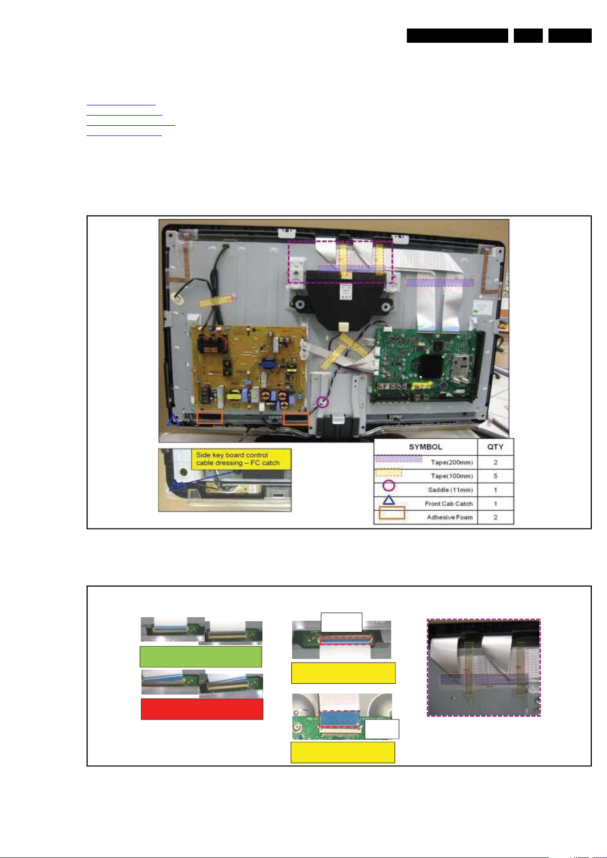
4.1.1 32PFL3805, Picasso/Dali Styling
Notes:
• Figures below can deviate slightly from the actual situation,
due to the different set executions.
Figure 4-1 Cable dressing 32" (32PFL3805, Picasso/Dali Styling)
Figure 4-2 FFC precautions 32" (32PFL3805, Picasso/Dali Styling)
2010-Mar-26
Page 10
EN 10 LC9.3L LA4.
18970_107_100323.eps
100323
18970_108_100323.eps
100323
Mechanical Instructions
Figure 4-3 Light leakage solution 32" (32PFL3805, Picasso/Dali Styling)
2010-Mar-26
Figure 4-4 Adding felt on front cabinet 32" (32PFL3805, Picasso/Dali Styling)
Page 11
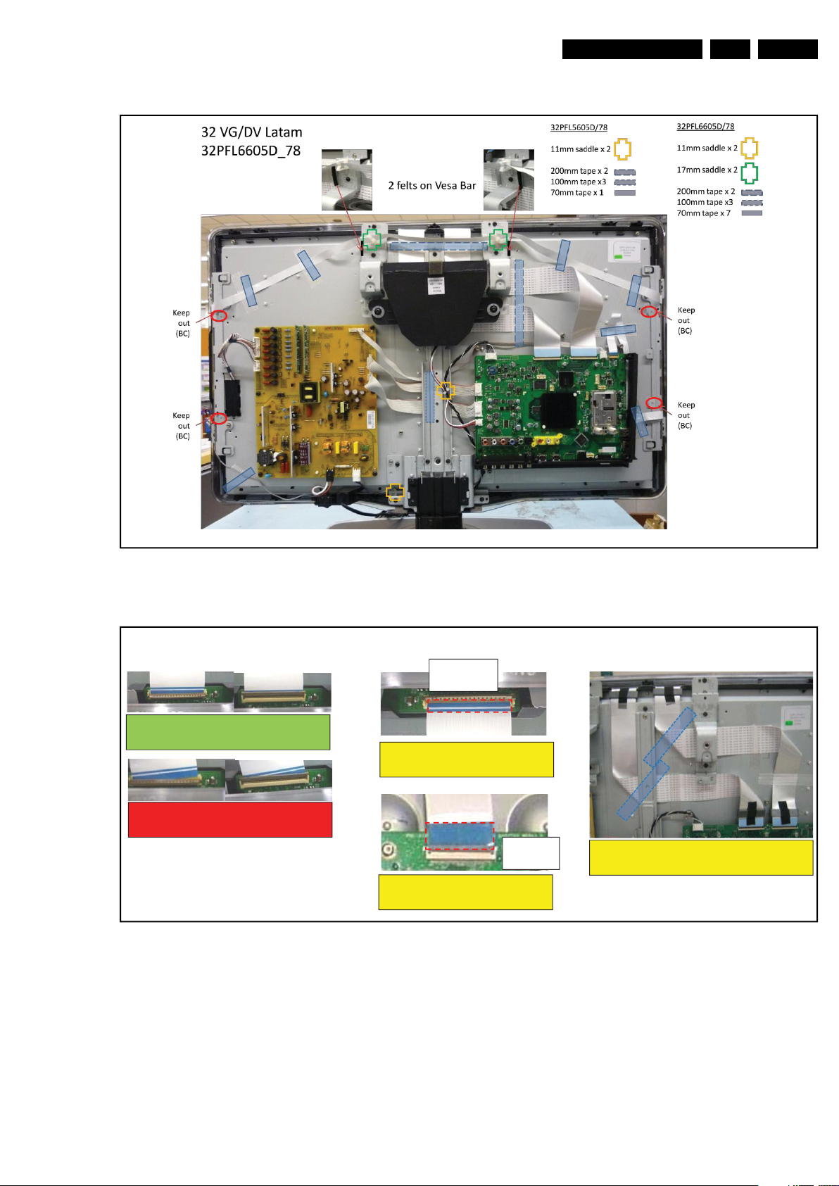
4.1.2 32PFL6605, Van Gogh/Da Vinci Styling
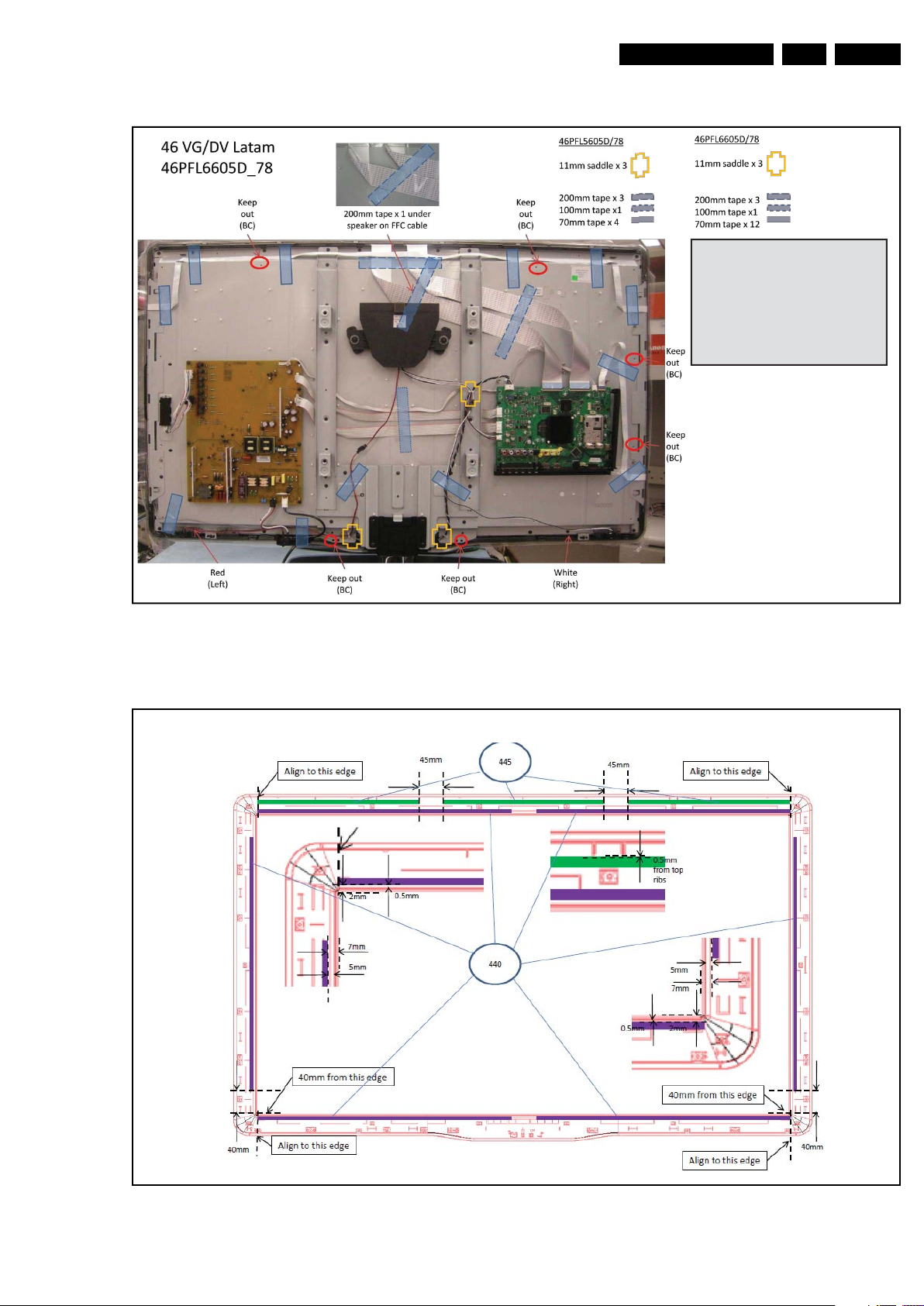
Note : Cable 8M09, 8M59 and 8M83 used in Da Vinci (Ambilight) only
18970_100_100323.eps
100323
FFC Pre-cautions
Proper FFC insertion: Silver line not
visible when connector lock is closed
Wrong FFC insertion: Silver line
visible when connector lock is closed
Thicker blue FFC supporting
tape belong to SSB side
Thinner blue FFC supporting
tape belong to Panel side
Panel
SSB
100 mm tape x 1 each under speaker on
FFC cable
18970_101_100323.eps
100323
Mechanical Instructions
EN 11LC9.3L LA 4.
Figure 4-5 Cable dressing 32" (32PFL6605, Van Gogh/Da Vinci Styling)
Figure 4-6 FFC precautions 32" (32PFL6605, Van Gogh/Da Vinci Styling)
2010-Mar-26
Page 12
EN 12 LC9.3L LA4.
Add Felt on Ambilight
Bracket (Da Vinci Only)
Applicable to both
Left & Right AL bracket
0443
18970_102_100323.eps
100323
Note : 1) Cable 8M09, 8M59 and 8M83 used in Da Vinci (Ambilight) only
2) Left (view from front of TV) Tweeter with White cable
3) Right (view from front of TV) Tweeter with Red cable + Insulation
18970_109_100323.eps
100323
Mechanical Instructions
Figure 4-7 Adding felt on front cabinet 32" (32PFL6605, Van Gogh/Da Vinci Styling)
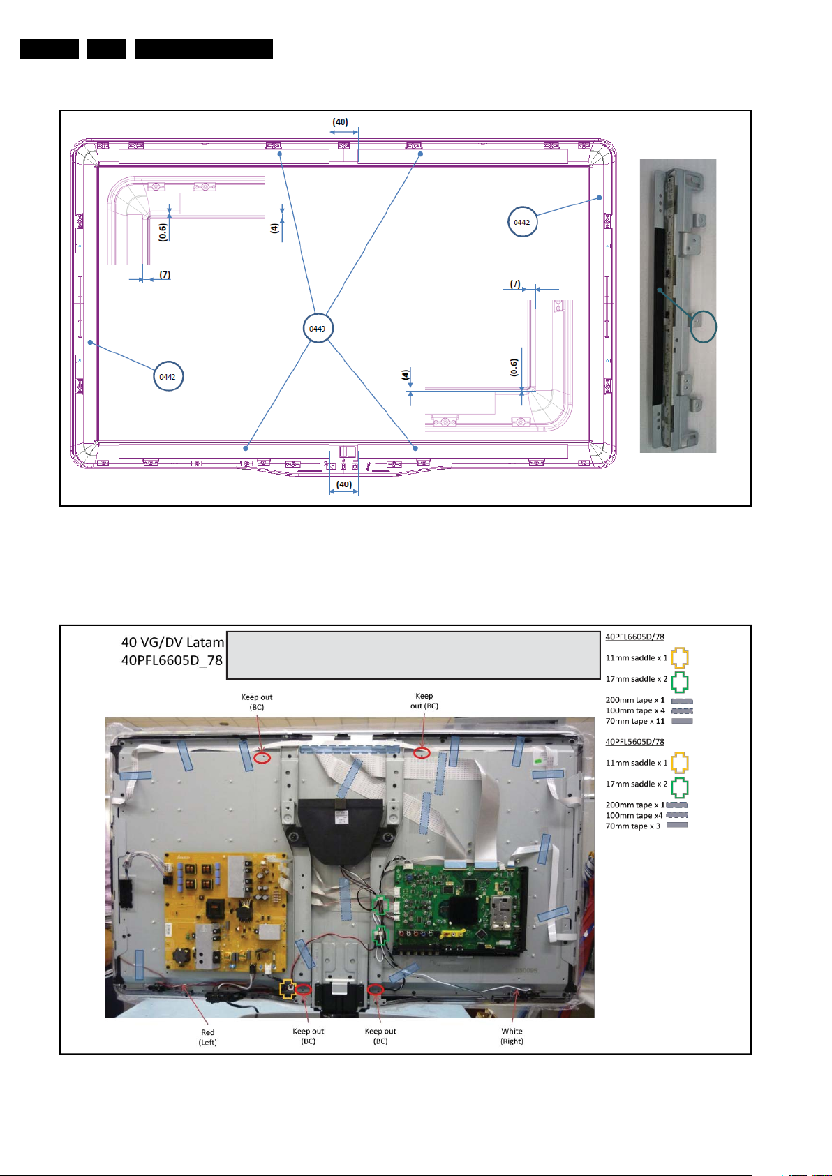
4.1.3 40PFL6605, Van Gogh/Da Vinci Styling
2010-Mar-26
Figure 4-8 Cable dressing 40" (40PFL6605, Van Gogh/Da Vinci Styling)
Page 13
4.1.4 46PFL6605, Van Gogh/Da Vinci Styling
1) Cable 8M09, 8M59 and 8M83
used in Da Vinci (Ambilight) only
2) Left (view from front of TV)
tweeter with white cable
3) Right (view from front of TV)
tweeter with red cable + insulation
Note :
18970_110_100323.eps
100323
Add Felts on Front Cabinet
18970_111_100323.eps
100323
Mechanical Instructions
EN 13LC9.3L LA 4.
Figure 4-9 Cable dressing 46" (46PFL6605, Van Gogh/Da Vinci Styling)
Figure 4-10 Adding felt on front cabinet 46" (46PFL6605, Van Gogh/Da Vinci Styling)
2010-Mar-26
Page 14
EN 14 LC9.3L LA4.
18970_113_100326.eps
100326
3
3
2
2
2
2
2
2
2
2
2
1
1
1
1
2
2
2
3
3
3
3
2
3
1
Mechanical Instructions
4.2 Service Positions
For easy servicing of a TV set, the set should be put face down
on a soft flat surface, foam buffers or other specific workshop
tools. Ensure that a stable situation is created to perform
measurements and alignments. When using foam bars take
care that these always support the cabinet and never only the
display.
Caution: Failure to follow these guidelines can seriously
damage the display!
Ensure that ESD safe measures are taken.
4.3 Assy/Panel Removal
Instructions below apply to the 32PFL6605D/xx, but will be
similar for other models.
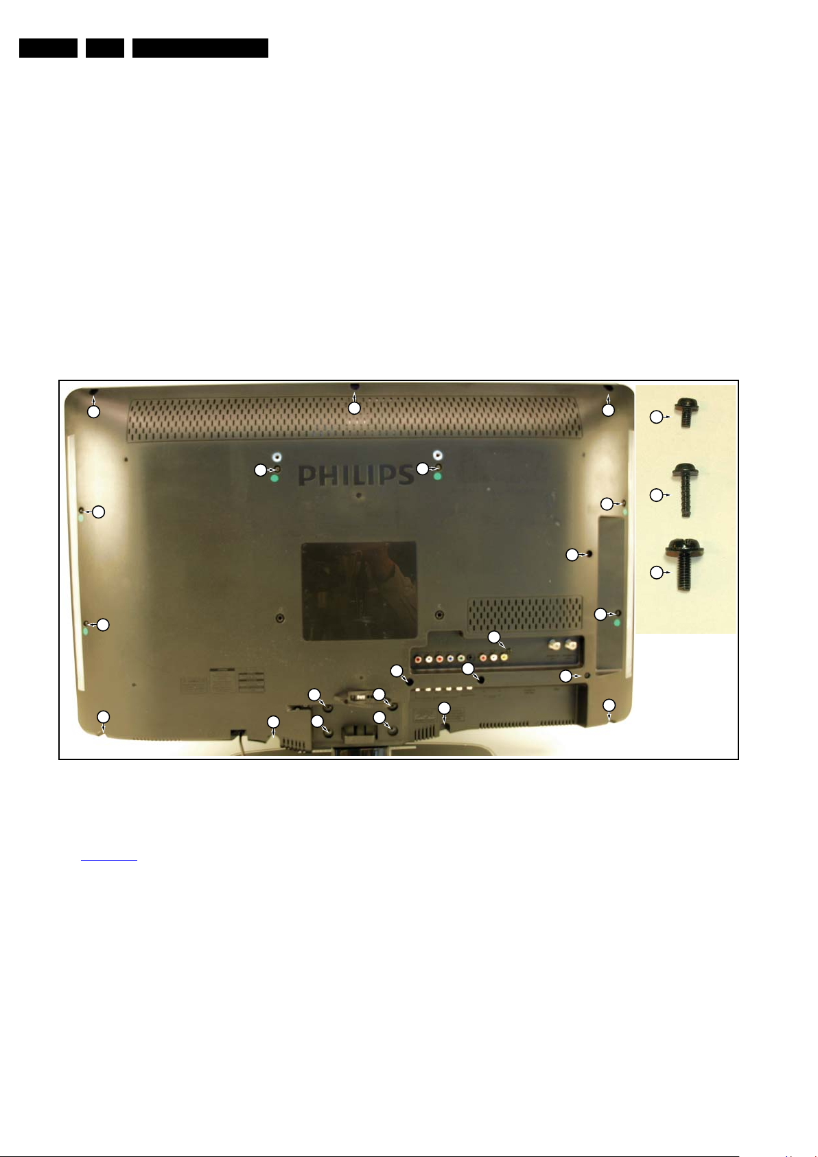
4.3.1 Rear Cover
Warning: Disconnect the mains power cord before removing
the rear cover.
See Figure 4-11
1. Remove fixation screws [2] and [3] that secure the rear
cover. It is not necessary to remove the stand first [1].
2. Lift the rear cover from the TV. Make sure that wires and
flat foils are not damaged while lifting the rear cover from
the set.
4.3.2 Speakers
Tweeters (when applicable)
Each tweeter unit is mounted with one screw.
When defective, replace the whole unit.
Loudspeaker/subwoofer
The loudspeaker/subwoofer is located in the centre of the set,
and is fixed with two screws.
When defective, replace the whole unit.
2010-Mar-26
.
Figure 4-11 Rear cover removal (32")
Page 15
Mechanical Instructions
18970_103_100323.eps
100323
1
2
2
2
2
2
2
1
3
3
1
1
18970_104_100323.eps
100323
2
2
1
3
3
3
3
3
2
18770_142_100215.eps
100215
1
1
1
1
18770_143_100215.eps
100215
2
18770_144_100215.eps
100215
4
3
3
EN 15LC9.3L LA 4.
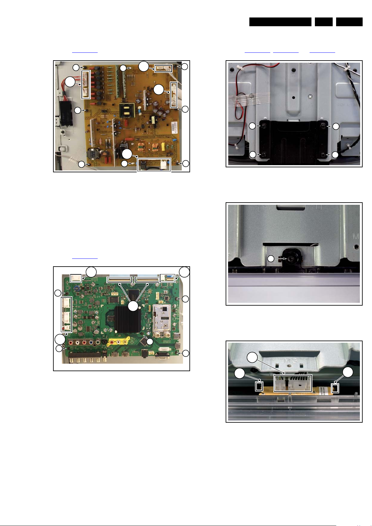
4.3.3 Main Power Supply
Refer to Figure 4-12
for details.
Figure 4-12 Main Power Supply
1. Unplug all connectors [1].
2. Remove the fixation screws [2].
3. Take the board out.
When defective, replace the whole unit.
Be aware to (re)place the spacers [3].
4.3.6 IR & LED Board
Refer to Figure 4-14
Figure 4-14 IR & LED Board -1-
, Figure 4-15 and Figure 4-16 for details.
4.3.4 Small Signal Board (SSB)
Refer to Figure 4-13
for details.
Figure 4-15 IR & LED Board -2-
Figure 4-13 SSB
1. Unplug all connectors [1] and [2].
2. Remove the fixation screws [3].
3. Take the board out.
When defective, replace the whole unit.
4.3.5 Mains Switch
The mains switch assy is mounted below the PSU on the front
bezel with two screws.
When replacing the switch, remove it from its bracket.
1. Remove the stand [1].
2. Remove the IR & LED board cover [2].
3. Release the clips [3] that secure the IR & LED board.
4. Remove the connectors [4] on the IR/LED board.
Figure 4-16 IR & LED Board -3-
2010-Mar-26
Page 16
EN 16 LC9.3L LA4.
18770_145_100216.eps
100217
1
18970_112_100326.eps
100326
1
1
1
1
2
2
1
2
2
1
1
1
C
D
A
B
E
1
F
4.3.7 Local Control Board
Mechanical Instructions
Refer to Figure 4-17
1. Unplug the connector on the IR & LED board that leads to
the Local Control board as described earlier.
2. Release the cable from its clamps/tape.
3. Release the clip on top of the unit [1] and take the unit out.
When defective, replace the whole unit.
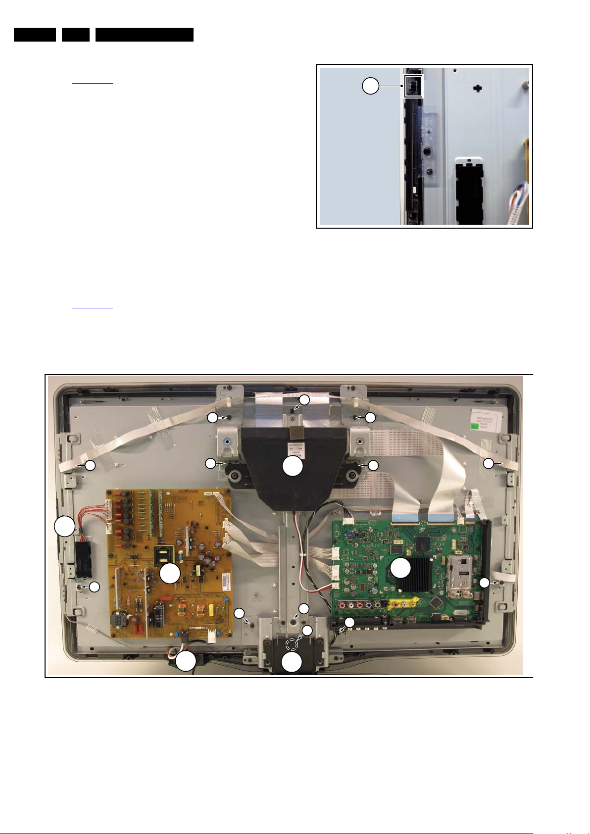
4.3.8 LCD Panel
Refer to Figure 4-18
1. Remove the Stand and IR/LED board [A] as earlier
described.
2. Remove the Speakers/Subwoofer [B] as earlier described.
3. Remove the PSU [C] and SSB [D] as earlier described.
4. Remove the Mains Switch [E] as earlier described.
for details.
for details.
Figure 4-17 Local Control board
5. Remove the Local Control board [F] as earlier described.
6. Remove the brackets [1].
7. Remove the clamps [2].
8. Remove the flare.
Now the LCD Panel can be lifted from the front cabinet.
Figure 4-18 LCD Panel removal (based on 32" AL model)
4.4 Set Re-assembly
2010-Mar-26
To re-assemble the whole set, execute all processes in reverse
order.
Notes:
• While re-assembling, make sure that all cables are placed
and connected in their original position.
• Pay special attention not to damage the EMC foams in the
set. Ensure that EMC foams are mounted correctly.
Page 17
Service Modes, Error Codes, and Fault Finding
5. Service Modes, Error Codes, and Fault Finding
EN 17LC9.3L LA 5.
Index of this chapter:
5.1 Test Points
5.2 Service Modes
5.3 Service Tools
5.4 Error Codes
5.5 The Blinking LED Procedure
5.6 Fault Finding and Repair Tips
5.7 Software Upgrading
5.1 Test Points
In the chassis schematics and layout overviews, the test points
are mentioned. In the schematics, test points are indicated with
“Fxxx” or “Ixxx”, in the layout overviews with a “half-moon” sign.
As most signals are digital, it will be difficult to measure
waveforms with a standard oscilloscope. Several key ICs are
capable of generating test patterns, which can be controlled via
ComPair. In this way it is possible to determine which part is
defective.
Perform measurements under the following conditions:
• Service Default Mode.
• Video: Color bar signal.
• Audio: 3 kHz left, 1 kHz right.
5.2 Service Modes
The Service Mode feature is split into four parts:
• Service Default Mode (SDM).
• Service Alignment Mode (SAM).
• Customer Service Mode (CSM).
• Computer Aided Repair Mode (ComPair).
SDM and SAM offer features, which can be used by the Service
engineer to repair/align a TV set. Some features are:
• A pre-defined situation to ensure measurements can be
made under uniform conditions (SDM).
• Activates the blinking LED procedure for error identification
when no picture is available (SDM).
• The possibility to overrule software protections when SDM
is entered via the Service pins.
• Make alignments (e.g. White Tone), (de)select options,
enter options codes, reset the error buffer (SAM).
• Display information (“SDM” or “SAM” indication in upper
right corner of screen, error buffer, software version,
operating hours, options and option codes, sub menus).
The CSM is a Service Mode that can be enabled by the
consumer. The CSM displays diagnosis information, which the
customer can forward to the dealer or call centre. In CSM
mode, “CSM”, is displayed in the top right corner of the screen.
The information provided in CSM and the purpose of CSM is to:
• Increase the home repair hit rate.
• Decrease the number of nuisance calls.
• Solved customers' problem without home visit.
ComPair Mode is used for communication between a computer
and a TV on I2C /UART level and can be used by a Service
engineer to quickly diagnose the TV set by reading out error
codes, read and write in NVMs, communicate with ICs and the
uP (PWM, registers, etc.), and by making use of a fault finding
database. It will also be possible to up and download the
software of the TV set via I2C with help of ComPair. To do this,
ComPair has to be connected to the TV set via the ComPair
connector, which will be accessible through the rear of the set
(without removing the rear cover).
5.2.1 Service Default Mode (SDM)
Purpose
Set the TV in SDM mode in order to be able to:
• Create a pre-defined setting for measurements to be
made.
• Override software protections.
• Start the blinking LED procedure.
• Read the error buffer.
• Check the life timer.
Specifications
Table 5-1 SDM default settings
Region Freq. (MHz) Default syst.
Europe (except France),
AP-PAL/-Multi
France SECAM L
NAFTA, AP-NTSC 61.25 (channel 3) NTSC M
LATAM PAL M
• Set linear video and audio settings to 50%, but volume to
25%. Stored user settings are not affected.
• All service-unfriendly modes (if present) are disabled, since
they interfere with diagnosing/repairing a set. These
service unfriendly modes are:
– (Sleep) timer.
– Blue mute/Wall paper.
– Auto switch “off” (when there is no “ident” signal).
– Hotel or hospital mode.
– Child lock or parental lock (manual or via V-chip).
– Skipping, blanking of “Not favorite”, “Skipped” or
“Locked” presets/channels.
– Automatic storing of Personal Preset or Last Status
settings.
– Automatic user menu time-out (menu switches back/
OFF automatically.
– Auto Volume levelling (AVL).
How to Activate SDM
For this chassis there are two kinds of SDM: an analog SDM
and a digital SDM. Tuning will happen according Table 5-1
• Analog SDM: use the standard RC-transmitter and key in
the code “062596”, directly followed by the “MENU” (or
HOME) button.
Note: It is possible that, together with the SDM, the main
menu will appear. To switch it “off”, push the “MENU” (or
HOME) button again.
• Digital SDM: use the standard RC-transmitter and key in
the code “062593”, directly followed by the “MENU” (or
HOME) button.
Note: It is possible that, together with the SDM, the main
menu will appear. To switch it “off”, push the “MENU” (or
HOME) button again.
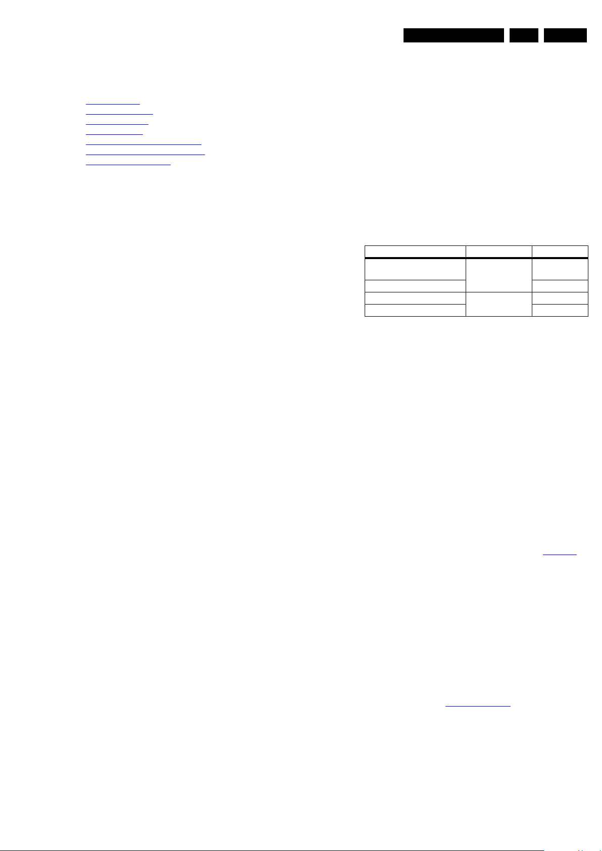
• Analog SDM can also be activated by grounding for a
moment the solder pad on the SSB, with the indication
“SDM” (see figure Service mode pad
475.25 PAL B/G
).
.
2010-Mar-26
Page 18
EN 18 LC9.3L LA5.
18970_200_100325.eps
100325
SDMSDM
10000_038_090121.eps
090819
PHILIPS
MODEL:
32PF9968/10
PROD.SERIAL NO:
AG 1A0620 000001
040
39mm
27mm
(CTN Sticker)
Display Option
Code
Figure 5-1 Service mode pad
After activating this mode, “SDM” will appear in the upper right
corner of the screen (when a picture is available).
How to Navigate
When the “MENU” (or HOME) button is pressed on the RC
transmitter, the TV set will toggle between the SDM and the
normal user menu.
How to Exit SDM
Use one of the following methods:
• Switch the set to STAND-BY via the RC-transmitter.
• Via a standard customer RC-transmitter: key in “00”sequence.
5.2.2 Service Alignment Mode (SAM)
Purpose
• To perform (software) alignments.
• To change option settings.
• To easily identify the used software version.
• To view operation hours.
• To display (or clear) the error code buffer.
Service Modes, Error Codes, and Fault Finding
• Operation Hours. Displays the accumulated total of
operation hours (not the stand-by hours). Every time the
TV is switched “on/off”, 0.5 hours is added to this number.
• Errors (followed by maximum 10 errors). The most recent
error is displayed at the upper left (for an error explanation
see section “5.4 Error Codes
• Reset Error Buffer. When “cursor right” (or the “OK
button) is pressed and then the “OK” button is pressed, the
error buffer is reset.
• Alignments. This will activate the “ALIGNMENTS” submenu. See chapter 6.3 Software Alignments
• Dealer Options. Extra features for the dealers.
• Options. Extra features for Service. For more information
about option codes, refer to 6.4 Option Settings
if the option code numbers are changed, these have to be
confirmed with pressing the “OK” button before the options
are stored. Otherwise changes will be lost.
• Initialize NVM. The moment the processor recognizes a
corrupted NVM, the “initialize NVM” line will be highlighted.
Now, two things can be done (dependent of the service
instructions at that moment):
– Save the content of the NVM via ComPair for
development analysis, before initializing. This will give
the Service department an extra possibility for
diagnosis (e.g. when Development asks for this).
– Initialize the NVM.
Note: When the NVM is corrupted, or replaced, there is a high
possibility that no picture appears because the display code is
not correct. So, before initializing the NVM via the SAM, a
picture is necessary and therefore the correct display option
has to be entered. To adapt this option bit, it is advised to use
ComPair (the correct values for the options can be found in
Table 6-5
Changing the display option via a standard RC: Key in the
code “062598” directly followed by the “MENU” (or HOME)
button and “XXX” (where XXX is the 3 digit decimal display
code as mentioned in Table 6-5
digits, also the leading zero’s. If the above action is successful,
the front LED will go out as an indication that the RC sequence
was correct. After the display option is changed in the NVM, the
TV will go to the Stand-by mode. If the NVM was corrupted or
empty before this action, it will be initialized first (loaded with
default values). This initializing can take up to 20 seconds.
) or a method via a standard RC (described below).
”).
.
. Note that
). Make sure to key in all three
2010-Mar-26
How to Activate SAM
Via a standard RC transmitter: Key in the code “062596”
directly followed by the “INFO” button. After activating SAM
with this method a service warning will appear on the screen,
continue by pressing the “OK” button on the RC.
Contents of SAM (see also Table 6-6
)
• Hardware Info.
– A. SW Version. Displays the software version of the
main software (example: LC93L-1.2.3.4=
AAAAB_X.Y.W.Z).
• AAAA= the chassis name.
• B= the region (A= Asian Pacific, E= Europe, L=
Latam, U= United States).
• X.Y.W.Z= the software version, where X is the
main version number (different numbers are not
compatible with one another) and Y.W.Z is the sub
version number (a higher number is always
compatible with a lower number).
– B. Standby Processor Version. Displays the
software version of the Stand-by processor.
– C. Production Code. Displays the production code of
the TV, this is the serial number as printed on the back
of the TV set. Note that if an NVM is replaced or is
initialized after corruption, this production code has to
be re-written to NVM. ComPair will foresee in a
possibility to do this.
Figure 5-2 Location of Display Option Code sticker
• Store - go right. All options and alignments are stored
when pressing “cursor right” (or the “OK” button) and then
the “OK”-button.
• SW Maintenance.
– SW Events. Not useful for Service purposes. In case
of specific software problems, the development
department can ask for this info.
– HW Events. Not useful for Service purposes. In case
of specific software problems, the development
department can ask for this info.
Page 19

Service Modes, Error Codes, and Fault Finding
EN 19LC9.3L LA 5.
• Operation hours display. Displays the accumulated total
of display operation hours. So, this one keeps up the
lifetime of the display itself, mainly to compensate the
degeneration behavior.
• Test settings. For development purposes only.
• Development file versions. Not useful for Service
purposes, this information is only used by the development
department.
• Upload to USB. To upload several settings from the TV to
an USB stick, which is connected to the SSB. The items are
“Channel list”, “Personal settings”, “Option codes”,
“Display-related alignments” and “History list”. First a
directory “repair\” has to be created in the root of the
USB stick. To upload the settings select each item
separately, press “cursor right” (or the “OK” button),
confirm with “OK” and wait until “Done” appears. In case
the download to the USB stick was not successful “Failure”
will appear. In this case, check if the USB stick is
connected properly and if the directory “repair” is present in
the root of the USB stick. Now the settings are stored onto
the USB stick and can be used to download onto another
TV or other SSB. Uploading is of course only possible if the
software is running and if a picture is available. This
method is created to be able to save the customer’s TV
settings and to store them into another SSB.
• Download to USB. To download several settings from the
USB stick to the TV, same way of working needs to be
followed as with uploading. To make sure that the
download of the channel list from USB to the TV is
executed properly, it is necessary to restart the TV and
tune to a valid preset if necessary.
Note: The “History list item” can not be downloaded from
USB to the TV. This is a “read-only” item. In case of
specific problems, the development department can ask
for this info.
How to Navigate
• In SAM, the menu items can be selected with the
“CURSOR UP/DOWN” key on the RC-transmitter. The
selected item will be highlighted. When not all menu items
fit on the screen, move the “CURSOR UP/DOWN” key to
display the next/previous menu items.
• With the “CURSOR LEFT/RIGHT” keys, it is possible to:
– (De) activate the selected menu item.
– (De) activate the selected sub menu.
• With the “OK” key, it is possible to activate the selected
action.
How to Exit SAM
Use one of the following methods:
• Switch the TV set to STAND-BY via the RC-transmitter.
• Via a standard RC-transmitter, key in “00” sequence, or
select the “BACK” key.
5.2.3 Customer Service Mode (CSM)
Purpose
The Customer Service Mode shows error codes and
information on the TV’s operation settings. A call centre can
instruct the customer (by telephone) to enter CSM in order to
identify the status of the set. This helps them to diagnose
problems and failures in the TV before making a service call.
The CSM is a read-only mode; therefore, modifications are not
possible in this mode.
• Possibility to use “CH+” or “CH-” for channel surfing, or
enter the specific channel number on the RC.
How to Activate
To activate CSM, press the following key sequence on a
standard remote control transmitter: “123654” (do not allow the
display to time out between entries while keying the sequence).
Contents of CSM
The contents are reduced to 3 pages: General, Software
versions and Quality items. The group names itself are not
shown anywhere in the CSM menu.
General
• Set Type. This information is very helpful for a helpdesk/
workshop as reference for further diagnosis. In this way, it
is not necessary for the customer to look at the rear of the
TV-set. Note that if an NVM is replaced or is initialized after
corruption, this set type has to be re-written to NVM.
ComPair will foresee in a possibility to do this.
• Production Code. Displays the production code (the serial
number) of the TV. Note that if an NVM is replaced or is
initialized after corruption, this production code has to be
re-written to NVM. ComPair will foresee a in possibility to
do this.
• Installed date. Indicates the date of the first installation of
the TV. This date is acquired via time extraction.
• Options 1. Gives the option codes of option group 1 as set
in SAM (Service Alignment Mode).
• Options 2. Gives the option codes of option group 2 as set
in SAM (Service Alignment Mode).
• 12NC SSB. Gives an identification of the SSB as stored in
NVM. Note that if an NVM is replaced or is initialized after
corruption, this identification number has to be re-written to
NVM. ComPair will foresee in a possibility to do this. This
identification number is the 12nc number of the SSB.
• 12NC display. Shows the 12NC of the display.
• 12NC supply. Shows the 12NC of the supply.
Software versions
• Current main SW. Displays the built-in main software
version. In case of field problems related to software,
software can be upgraded. As this software is consumer
upgradable, it will also be published on the Internet.
Example: LC92L_1.2.3.4
• Ambilight SW. Displays the Ambilight SW-version.
Quality items
• Signal quality. Poor / average /good
• Child lock. Not active / active. This is a combined item for
locks. If any lock (Preset lock, child lock, lock after or
parental lock) is active, the item shall show “active”.
• HDMI HDCP key. Indicates if the HDMI keys (or HDCP
keys) are valid or not. In case these keys are not valid and
the customer wants to make use of the HDMI functionality,
the SSB has to be replaced.
• Ethernet MAC address. Displays the MAC address
present in the SSB.
• BDS key. Indicates if the “BDS level” key is valid or not.
How to Exit CSM
Press “MENU” (or HOME) / “Back” key on the RC-transmitter.
Specifications
• Ignore “Service unfriendly modes”.
• Line number for every line (to make CSM language
independent).
• Set the screen mode to full screen (all contents on screen
is visible).
• After leaving the Customer Service Mode, the original
settings are restored.
2010-Mar-26
Page 20
EN 20 LC9.3L LA5.
Service Modes, Error Codes, and Fault Finding
5.3 Service Tools
5.3.1 ComPair
Introduction
ComPair (Computer Aided Repair) is a Service tool for Philips
Consumer Lifestyle products. and offers the following:
1. ComPair helps you to quickly get an understanding on how
to repair the chassis in a short and effective way.
2. ComPair allows very detailed diagnostics and is therefore
capable of accurately indicating problem areas. You do not
have to know anything about I2C or UART commands
yourself, because ComPair takes care of this.
3. ComPair speeds up the repair time since it can
automatically communicate with the chassis (when the uP
is working) and all repair information is directly available.
4. ComPair features TV software up possibilities.
Specifications
ComPair consists of a Windows based fault finding program
and an interface box between PC and the (defective) product.
The (new) ComPair II interface box is connected to the PC via
an USB cable. For the TV chassis, the ComPair interface box
and the TV communicate via a bi-directional cable via the
service connector(s).
How to Connect
This is described in the ComPair chassis fault finding database.
TO TV
TO
TO
UART SERVICE
CONNECTOR
2
C
I
RS232 /UART
ComPair II
RC in
Optional
Switch
Power ModeLink/
Activity
UART SERVICE
CONNECTOR
RC out
TO
I2C SERVICE
CONNECTOR
Multi
function
5.4 Error Codes
5.4.1 Introduction
The error code buffer contains all detected errors since the last
time the buffer was erased. The buffer is written from left to
right, new errors are logged at the left side, and all other errors
shift one position to the right.
When an error occurs, it is added to the list of errors, provided
the list is not full. When an error occurs and the error buffer is
full, then the new error is not added, and the error buffer stays
intact (history is maintained).
To prevent that an occasional error stays in the list forever, the
error is removed from the list after more than 50 hrs. of
operation.
When multiple errors occur (errors occurred within a short time
span), there is a high probability that there is some relation
between them.
New in this chassis is the way errors are displayed:
• There is a simple blinking LED procedure for board level
repair (home repair) so called LAYER 1 errors, next to the
existing errors which are LAYER 2 errors (see Table 5-3
– LAYER 1 errors are one digit errors (via CSM).
– LAYER 2 errors are 2 digit errors (via SAM/SDM).
• In protection mode:
– From consumer mode: LAYER 1.
– From SDM mode: LAYER 2.
• In CSM mode: When entering CSM: error LAYER 1 will be
displayed by blinking LED. Only the latest error is shown.
• In SDM mode: When SDM is entered via Remote Control
code or the hardware pins, LAYER 2 is displayed via
blinking LED.
• In the “ON” state: with the RC commands “mute_06250X
_OK”, LAYER 2 errors are displayed via blinking LED.
• Error display on screen:
– In CSM no error codes are displayed on screen.
– In SAM the complete error list is shown.
).
PC
ComPair II Developed by Philips Brugge
Optional power
HDMI
2
I
C only
5V DC
10000_036_090121.eps
091118
Figure 5-3 ComPair II interface connection
Caution: It is compulsory to connect the TV to the PC as
shown in the picture above (with the ComPair interface in
between), as the ComPair interface acts as a level shifter. If
one connects the TV directly to the PC (via UART), ICs will be
blown!
How to Order
ComPair II order codes:
• ComPair II interface: 3122 785 91020.
• ComPair UART interface cable: 3138 188 75051.
• Program software can be downloaded from the Philips
Service portal.
Note: If you encounter any problems, contact your local
support desk.
5.4.2 How to Read the Error Buffer
Use one of the following methods:
• On screen via the SAM (only when a picture is visible).
E.g.:
– 00 00 00 00 00: No errors detected
– 23 00 00 00 00: Error code 23 is the last and only
detected error.
– 37 23 00 00 00: Error code 23 was first detected and
error code 37 is the last detected error.
– Note that no protection errors can be logged in the
error buffer.
• Via the blinking LED procedure. See section 5.4.3 How to
Clear the Error Buffer.
•Via ComPair.
5.4.3 How to Clear the Error Buffer
Use one of the following methods:
• By activation of the “Reset error buffer” command in the
SAM menu.
• With a normal RC, key in sequence “MUTE” followed by
“062599” and “OK”.
• If the content of the error buffer has not changed for 50+
hours, it resets automatically.
2010-Mar-26
Page 21
5.4.4 Error Buffer
Service Modes, Error Codes, and Fault Finding
EN 21LC9.3L LA 5.
In case of non-intermittent faults, clear the error buffer before
Table 5-2 Layer 1 error codes
starting to repair (before clearing the buffer, write down the
content, as this history can give significant information). This to
ensure that old error codes are no longer present.
If possible, check the entire contents of the error buffer. In
some situations, an error code is only the result of another error
code and not the actual cause (e.g. a fault in the protection
Description Layer 1 code Remarks
SSB 2
Display supply 3 If only one supply is used
Platform supply 4 No separate supply
Ambilight 8
detection circuitry can also lead to a protection).
Take notice that some errors need several minutes before they
start blinking or before they will be logged. So in case of
problems wait 2 minutes from start-up onwards, and then
check if the front LED is blinking or if an error is logged.
Table 5-3 Error code overview
Description Layer 1 Layer 2 Monitored
by
I2C Bus related:
I2C bus blocked (front-end) 2 12 ARM E BL/EB SSB SSB
I2C1 bus blocked 2 13 ARM E BL/EB SSB SSB
I2C0 bus blocked 2 14 ARM E BL SSB SSB
System does not boot 2 15 ARM/Stby µP P BL SSB SSB
I2C2 bus blocked (EDID HDMI) 2 18 ARM E BL/EB SSB SSB
Supply related:
DC on speaker 2 11 ARM P BL / SSB
POK (inverter or display supply) 3 17 ADC E EB / Supply
IC related:
HDMI MUX 2 23 ARM E EB ADV3002 SSB
HDMI EDID 2 24 ARM E EB M24C02-WMN6 SSB
ARM (Ambilight) 8 28 ARM E EB NXP LPC2103 AL-module or DC/DC
Tuner (Frontend) 2 34 ARM E EB VA1G5BF8010 SSB
Main NVM 2 35 ARM E / M24C64 SSB
Error/
Prot
Error Buffer/
Blinking LED
Device Defective Board
5.5 The Blinking LED Procedure
5.5.1 Introduction
The software is capable of identifying different kinds of errors.
Because it is possible that more than one error can occur over
time, an error buffer is available, which is capable of storing the
last five errors that occurred. This is useful if the OSD is not
working properly.
Errors can also be displayed by the blinking LED procedure.
The method is to repeatedly let the front LED pulse with as
many pulses as the error code number, followed by a period of
1.5 seconds in which the LED is “off”. Then this sequence is
repeated.
Example (1): error code 4 will result in four times the sequence
LED “on” for 0.25 seconds / LED “off” for 0.25 seconds. After
this sequence, the LED will be “off” for 1.5 seconds. Any RC5
command terminates the sequence. Error code LED blinking is
in red color.
Example (2): the content of the error buffer is “129600”
After entering SDM, the following occurs:
• 1 long blink of 5 seconds to start the sequence,
• 12 short blinks followed by a pause of 1.5 seconds,
• 9 short blinks followed by a pause of 1.5 seconds,
• 6 short blinks followed by a pause of 1.5 seconds,
• 1 long blink of 1.5 seconds to finish the sequence,
• The sequence starts again with 12 short blinks.
In order to avoid confusion with RC5 signal reception blinking,
this blinking procedure is terminated when a RC5 command is
received.
5.5.2 Displaying the Entire Error Buffer
Additionally, the entire error buffer is displayed when Service
Mode “SDM” is entered. In case the TV set is in protection or
Stand-by: The blinking LED procedure sequence (as in SDMmode in normal operation) must be triggered by the following
RC sequence: “MUTE” “062500” “OK”.
2010-Mar-26
Page 22

EN 22 LC9.3L LA5.
Service Modes, Error Codes, and Fault Finding
5.6 Fault Finding and Repair Tips
Notes:
• It is assumed that the components are mounted correctly
with correct values and no bad solder joints.
• Before any fault finding actions, check if the correct
options are set.
5.6.1 Software Protections
Most of the protections and errors use either the stand-by or the
micro processor as detection device. Since in these cases,
checking of observers, polling of ADCs, and filtering of input
values are all heavily software based, these protections are
referred to as software protections.
There are several types of software related protections, solving
a variety of fault conditions:
• Protections related to supplies: check of the 12V.
• Protections related to breakdown of the safety check
mechanism. E.g. since the protection detections are done
by means of software, failing of the software will have to
initiate a protection mode since safety cannot be
guaranteed any more.
Remark on the Supply Errors
The detection of a supply dip or supply loss during the normal
playing of the set does not lead to a protection, but to a cold
reboot of the set. If the supply is still missing after the reboot,
the TV will go to protection.
Protections during Start-up
During TV start-up, some voltages and IC observers are
actively monitored to be able to optimize the start-up speed,
and to assure good operation of all components. If these
monitors do not respond in a defined way, this indicates a
malfunction of the system and leads to a protection.
5. Stop bits = 1
6. Flow control = none
During the start-up of the TV set, the logging will be displayed.
This is also the case during rebooting of the TV set (the same
logging appears time after time). Also available in the logging
is the “Display Option Code” (useful when there is no picture),
look for item “DisplayRawNumber” in the beginning of the
logging. Tip: when there is no picture available during
rebooting you are able to check for “error devices” in the
logging (LAYER 2 error) which can be very helpful to determine
the failure cause of the reboot. For protection state, there is no
logging.
5.6.4 Display option code
Caution: In case you have replaced the SSB, always check the
display option code in SAM, even if you have picture. With a
wrong display option code it is possible that you have picture,
but that in certain conditions you have unwanted side-effects.
5.6.5 Trouble Shooting Tuner section
When there is no picture in analog RF mode:
1. Check whether picture is present in AV mode. If not, tuner
section is okay. Check video processing section.
2. Check if option settings are correct.
3. Check if 5 and 33 V supplies are available.
4. Check if the I
5. Manually store a known channel and check if there is IF
output at tuner pin 11. If not, tuner is faulty.
6. Feed in 105 dBuV at tuner pin 11 and check whether there
is CVBS output from IF demodulator IC. If not, IF
demodulator might be faulty. Check components in this
area.
2
C lines are working correctly (3.3 V).
5.7 Software Upgrading
5.6.2 Hardware Protections
The only real hardware protection in this chassis is (in case of
an audio problem) the audio protection circuit that will trigger
the uP to switch “off” the TV.
Repair Tip
• It is also possible that you have an audio DC protection
because of an interruption in one or both speakers (the DC
voltage that is still on the circuit cannot disappear through
the speakers).
Caution: (dis)connecting the speaker wires during the ON
state of the TV at high volume can damage the audio
amplifier.
5.6.3 Logging
When something is wrong with the TV set (f.i.the set is
rebooting) you can check for more information via the logging
in Hyperterminal. The Hyperterminal is available in every
Windows application via Programs, Accessories,
Communications, Hyperterminal. Connect a “ComPair UART”cable (3138 188 75051) from the service connector in the TV to
the “multi function” jack at the front of ComPair II box.
Required settings in ComPair before starting to log:
- Start up the ComPair application.
- Select the correct database (open file “Q549.3E LA”, this will
set the ComPair interface in the appropriate mode).
- Close ComPair
After start-up of the Hyperterminal, fill in a name (f.i. “logging”)
in the “Connection Description” box, then apply the following
settings:
1. COMx
2. Bits per second = 115200
3. Data bits = 8
4. Parity = none
5.7.1 Introduction
It is possible for the user to upgrade the main software via the
USB port. This allows replacement of a software image in a
stand alone set, without the need of an E-JTAG debugger. A
description on how to upgrade the main software can be found
in the DFU.
Important: When the NAND-Flash must be replaced, a new
SSB must be ordered, due to the presence of the security keys!
(copy protection keys, MAC address, ...).
Perform the following actions after SSB replacement:
1. Set the correct option codes (see sticker inside the TV).
2. Update the TV software => see the DFU for instructions.
3. Perform the alignments as described in chapter 6.
4. Check in CSM if the HDMI key, MAC address.. are valid.
For the correct order number of a new SSB, always refer to the
Spare Parts list on the Philips Service web portal!
5.7.2 Software Upgrade
SW versions can be divided in three types:
• SW that can not crash the working of the set.
– EDID NVM. If the download fails, the set is still running
and the download can start again.
– Main NVM: If the download fails the default NVM value
can be loaded. NVM can be loaded via USB, be aware
PCBA alignments stored in NVM will not be overridden.
• SW that is “fool proof”: There is a backup version, a main
interruption during upgrade shall not crash the normal
working, a new upgrade can be started.
– Main SW image: Upgradable via USB.
– Standby SW.
– ARM Ambilight (if applicable): Upgradable via USB.
• SW that is not “fool proof”.
2010-Mar-26
Page 23

Service Modes, Error Codes, and Fault Finding
– Bootloader: Upgradable via USB in SAM (Note: must
be done by service personnel).
SW for all model numbers is loaded to the Philips Service portal
(P4S) and contains the following software:
• Process_NVM_LC09Mxxx.bin: mainly for factory use to
load main NVM. Can be used by service if applicable.
• LC09M_VGAxxxx.bin: for loading VGA NVM using
ComPair tool.
• LC09M_HDMIxxxx.bin: for loading HDMI NVM via
ComPair (HDMI MUX EDID) tool.
• The Autorun.upg file, which is available on P4C (the
consumer web site), contains:
– Main SW.
– Standby SW.
– Bootloader SW (via SAM upgradable).
– Ambilight SW (if applicable).
EN 23LC9.3L LA 5.
2010-Mar-26
Page 24
EN 24 LC9.3L LA6.
6. Alignments
Alignments
Index of this chapter:
6.1 General Alignment Conditions
6.2 Hardware Alignments
6.3 Software Alignments
6.4 Option Settings
Note: Figures below can deviate slightly from the actual
situation, due to the different set executions.
General: The Service Default Mode (SDM) and Service
Alignment Mode (SAM) are described in chapter 5. Menu
navigation is done with the CURSOR UP, DOWN, LEFT or
RIGHT keys of the remote control transmitter.
6.1 General Alignment Conditions
Perform all electrical adjustments under the following
conditions:
• Power supply voltage: 120 - 230 V
/ 50 Hz (± 10%).
AC
• Connect the set to the mains via an isolation transformer
with low internal resistance.
• Allow the set to warm up for approximately 15 minutes.
• Measure voltages and waveforms in relation to correct
ground (e.g. measure audio signals in relation to
AUDIO_GND).
Caution: It is not allowed to use heatsinks as ground.
• Test probe: Ri > 10 Mohm, Ci < 20 pF.
• Use an isolated trimmer/screwdriver to perform
alignments.
6.2 Hardware Alignments
There are no hardware alignments foreseen for this chassis,
but below find an overview of the most important DC voltages
on the SSB. These can be used for checking proper functioning
of the DC/DC converters.
Description Test Point Specifications (V) Diagram
+12VS F118 11.70 12.30 12.91 B01_DC-DC
+3V3_STBY F113 3.20 3.30 3.40 B01_DC-DC
+3V3_SW F127 3.17 3.34 3.5 B01_DC-DC
+1V2_SW F139 1.18 1.25 1.31 B01_DC-DC
+5V_SW F130 4.98 5.25 5.51 B01_DC-DC
+1V8_SW F101 1.74 1.83 1.92 B01_DC-DC
+1V0_SW F124 0.99 1.05 1.10 B01_DC-DC
+8V_SW F126 7.6 8.0 8.4 B01_DC-DC
+5VS F232 4.94 5.2 5.46 B02_Tuner_IF
+1V2SW F220 1.14 1.2 1.26 B02_Tuner_IF
+2V5_SW F208 2.38 2.5 2.62 B02_Tuner_IF
+3V3_SW F209 3.14 3.3 3.46 B02_Tuner_IF
+5VTUN_DIGITALF203 4.75 5 5.25 B02_Tuner_IF
VLS_15V6 FKFD 14.82 15.6 16.38 B14B_TCON_DC/DC
VGH_35V FKFA 33.25 35.0 36.75 B14B_TCON_DC/DC
VGL_-6V FKFK -6.32 -6.02 -5.72 B14B_TCON_DC/DC
VCC_3V3 FKFB 3.14 3.3 3.47 B14B_TCON_DC/DC
VCC_1V2 FKDD 1.14 1.2 1.26 B14A_TCON_CONTROL
Min. Typ. Max.
6.3 Software Alignments
• Press OK on the RC before the cursor is moved to the left.
• In main menu select “Store” and press OK on the RC.
• Press MENU on the RC to switch back to the main menu.
• Switch the set to stand-by mode.
For the next alignments, supply the following test signals via a
video generator to the RF input:
• LATAM models: an NTSC M TV-signal with a signal
strength of at least 1 mV and a frequency of 61.25 MHz
(channel 3).
6.3.1 White Point
• Set “Active control” to “Off”.
• Choose “TV menu”, “TV Settings” and then “Picture” and
set picture settings as follows:
Picture Setting
Dynamic backlight Off
Dynamic Contrast Off
Colour Enhancement Off
Picture Format Unscaled
Light Sensor Off
Brightness 50
Colour 0
Contrast 100
• Go to the SAM and select “Alignments”-> “White point”.
White point alignment LCD screens:
• Use a 100% white screen as input signal and set the
following values (in SAM mode):
– “Color temperature” to “Cool”.
– “Whitepoint red”, “Whitepoint green”, and “Whitepoint
blue” values to “127”.
– “Red BL offset” and “Green BL offset” values to “7”.
With a color analyzer:
Depending on which color analyzer you use (CS-200 or CA-
210), and what kind of panel is mounted in the set (CCFL with
panel codes 231/232, or LED with panel codes 233/234/236),
different values apply. Refer to
• Measure with a calibrated, contactless (max. 25 mm
distance) color analyzer in the centre of the screen.
Consequently, the measurement needs to be done in a
dark environment.
• Adjust one or two registers (so holding one of the White
point registers R, G or B on 127) to obtain the “Cool” x,y
values (see Table 6-1
). Tolerance: dx: ± 0.004, dy: ± 0.004.
• Repeat this step for the “Normal” and “Warm” color
temperatures.
• When finished press “OK” on the RC and then press
“Store” (in the SAM root menu) to store the aligned values
into the NVM.
• Restore the initial picture settings after the alignments.
Table 6-1 White D alignment values, CS-200 color analyzer
all panels
Value Cool (11000 K) Normal (9000 K) Warm (6500 K)
x 0.276 0.287 0.313
y 0.282 0.296 0.329
Put the set in SAM mode (see chapter 5. Service Modes, Error
Codes, and Fault Finding). The SAM menu will now appear on
the screen. Select ALIGNMENTS and go to one of the sub
menus. The alignments are explained below.
The following item can be aligned:
• Whitepoint.
To store the data:
2010-Mar-26
Table 6-2 White D alignment values, CA-210 color analyzer
CCFL panel (panel codes 231/232)
Value Cool (10100 K) Normal (8510 K) Warm (6250 K)
x 0.280 0.290 0.317
y 0.287 0.300 0.333
Page 25
Alignments
EN 25LC9.3L LA 6.
Table 6-3 White D alignment values, CA-210 color analyzer
LED panel (panel codes 233/234/236)
Value Cool (9330 K) Normal (7940 K) Warm (6060 K)
x 0.282 0.293 0.320
y 0.298 0.313 0.346
Without a color analyzer, you can use below default values.
This is the next best solution. The default values are average
values coming from production (statistics).
• Select a “Color Temperature” (e.g. “Cool”, “Normal”, or
“Warm”).
• Set the “Whitepoint Red”, “- Green” and “- Blue” default
values according to the values in the “Tint settings” table.
• When finished press “OK” on the RC, then press “Store” (in
the SAM root menu) to store the aligned values into the
NVM.
• Restore the initial picture settings after the alignments.
Table 6-4 Tint settings (default values)
Colour Temp. R G B
32-inch
Cool tbf tbf tbf
Normal tbf tbf tbf
Warm tbf tbf tbf
40-inch
Cool tbf tbf tbf
Normal tbf tbf tbf
Warm tbf tbf tbf
46-inch
Cool tbf tbf tbf
Normal tbf tbf tbf
Warm tbf tbf tbf
6.4.3 (Service) Options
Select the sub menu's to set the initialization codes (options) of
the model number via text menus.
See Table 6-6
.
6.4.4 Opt. No. (Option numbers)
Select this sub menu to set all options at once (expressed in
two long strings of numbers).
An option number (or “option byte”) represents a number of
different options. When you change these numbers directly,
you can set all options very quickly. All options are controlled
via eight option numbers.
When the NVM is replaced, all options will require resetting. To
be certain that the factory settings are reproduced exactly, you
must set both option number lines. You can find the correct
option numbers on a sticker inside the TV set and in Table
“Option code overview”.
Example: The options sticker gives the following option
numbers:
• 25604 00386 00235 56068
• 08395 05120 00000 00000
The first line (group 1) indicates hardware options 1 to 4.
Example: option no. “2” contains the “cabinet type”.
The second line (group 2) indicates software options 5 to 8.
Example: option no. “5” contains the “display code”.
Every 5-digit number represents 16 bits (so the maximum value
will be 65536 if all options are set).
When all the correct options are set, the sum of the decimal
values of each Option Byte (OB) will give the option number.
See Table 6-5
for the options. Always refer to the sticker in the
TV-set as leading.
6.4 Option Settings
6.4.1 Introduction
The microprocessor communicates with a large number of I
ICs in the set. To ensure good communication and to make
digital diagnosis possible, the microprocessor has to know
which ICs to address. The presence/absence of these specific
ICs (or functions) is made known by the option codes.
Notes:
• After changing the option(s), save them with the STORE
command.
• The new option setting becomes active after the TV is
switched “off” and “on” again with the mains switch (the
EAROM is then read again).
6.4.2 Dealer Options
For dealer options, in SAM select “Dealer options”.
See Table 6-6
.
6.5 Total Overview SAM modes
Table 6-6 SAM mode overview (usage is model dependent)
Diversity
Not all sets with the same Commercial Type Number (CTN)
necessarily have the same option code!
2
C
Use of Alternative BOM
An alternative BOM number usually indicates the use of an
alternative display. This results in another Display Code thus in
another Option code. Refer to chapter 3. Precautions, Notes,
and Abbreviation List.
6.4.5 Option code overview
Table 6-5 Option code overview (subject to change)
Model Number Option Codes Displ.
32PFL3805D/78 0102 8 00385 00171 56068 08423 04096 00000 00000 231
32PFL5605D/78 0922 0 08578 00171 56068 08425 04096 00000 00000 233
32PFL6605D/78 0925 2 08578 00171 56068 08425 04096 00000 00000 233
40PFL3805D/78 0102 8 00385 00171 56068 08424 04096 00000 00000 232
40PFL5605D/78 0922 0 08579 00171 56068 08426 04096 00000 00000 234
40PFL6605D/78 0926 8 08579 00171 56068 08426 04096 00000 00000 234
46PFL5605D/78 0922 0 08579 00171 56068 08428 04096 00000 00000 236
46PFL6605D/78 0928 4 08579 00171 56068 08428 04096 00000 00000 236
Code
Main Menu Sub-menu 1 Sub-menu 2 Sub-menu 3 Description
Hardware Info A. SW VERSION e.g. “QL92L_1.33.0.0” Displays TV & Standby SW version and CTN serial
B. Standby processor version e.g. “STDBY_88.68.0.0”
C. Production code e.g. “VN010935123456”
Operation hours Displays the accumulated total o f operation hours.TV
Errors Displayed the most recent errors.
number.
switched “on/off” & every 0.5 hours is increase one
2010-Mar-26
Page 26
EN 26 LC9.3L LA6.
Main Menu Sub-menu 1 Sub-menu 2 Sub-menu 3 Description
Reset error buffer Clears all content in the error buffer.
Alignment Tuner AGC RF-AGC Take over point adjustment (AGC default
White point Colour temperature Normal 3 different modes of colour temperature can be se-
Dealer options Personal options Picture mute Off/On Select Picture mute On/Off. Picture is muted / not
Options Digital broadcast DVB Off/On Select DVB On/Off
Digital features USB Off/On Select USB On/Off
Data EPG Off/On Select EPG On/Off
Display Screen e.g. “130 - LGD WUE SAA1 42"“ Displayed the panel code & type model.
Video reproduction Picture processing None/PNX5100 Select Picture processing None/PNX5100 (Q549.xE
Alignments
value is 80)
Warn
Cool
White point red
White point green
White point blue
Red black level offset
Green black level offset
Virgin mode Off/On
E-sticker Off/On Select E-sticker On/Off (USPs on-screen)
Auto store mode None
PDC/VPS
TXT page
PDC/VPS/TXT
DVB - T installation Off/On or Country dependent Select DVB T installation On/Off or by country
DVB - T light Off/On Select DVB T light On/Off
DVB - C Off/On Select DVB C On/Off
DVB - C installation Off/On or Country dependent Select DVB C installation On/Off or by country
Over the air download Off/On or Country dependent Select Over the air download On/Off or by country
8 days EPG Off/On Select 8 day EPG On/Off
Ethernet Off/On Select Ethernet On/Off
Wi-Fi Off/On Select Wi-Fi On/Off
DLNA Off/On Select DLNA On/Off
On-line service Off On-line service is Off
PTP (Picture Transfer Protocol) Off/On Select PTP On/Off
Update assistant Off/On Select Update assistant On/Off
Internet software update Off Internet software update is Off
TvTv EPG Off/On Select TvTv EPG On/Off
Dimming backlight Off/On Select Dimming Backlight On/Off
LightGuide Off/On Select LightGuide On/Off
Display fans Not present/Present Select Display fans Present/Not present.
Temperature sensor Sensor present in display (only for
Temperature LUT 0 N.A
E-box & monitor Off/On Select E-box & monitor On/Off
MOP local contrast Off/On Select MOP local contrast On/Off
Light sensor Off/On Select Light sensor On/Off
Light sensor type 0/1/2/3 Select Light sensor type form 0 to 3 (for difference
Pixel Plus type Pixel Plus HD Select type of picture improvement.
Pixel Plus Off/On Select Pixel Plus On/Off
Ambilight Off/Mono/Stereo/Triple/Quad/Pixe-
Ambilight technology CCFL/LED Select Ambilight technology.
Ambilight driver Pacific 3/MOP/DFI Select Ambilight driver.
Pacific 3 Not present/Present Select Pacific 3 presence.
MOP Not present/Present Select MOP presence.
MOP ambilight Off/On Select MOP ambilight On/Off
21:9)
Perfect Pixel HD
Pixel Precise HD
lated quad
lected
LCD White Point Alignment. For values,
see Table 6-4.
muted in case no input signal is detected at input
connectors.
Select Virgin mode On/Off. TV starts up / does not
start up (once) with a language selection menu after
the mains switch is turned “on” for the first time (virgin
mode)
N.A.
chassis).
styling).
Select type of Ambilight modules use.
2010-Mar-26
Page 27

Alignments
Main Menu Sub-menu 1 Sub-menu 2 Sub-menu 3 Description
Audio reproduction Acoustic system Cabinet design used for setting dynamic audio pa-
Source selection EXT1/AV1 type SCART CVBS RGB LR Select input source when connected with external
CVBS Y/C YPbPr LR
CVBS Y/C YPbPr HV LR
(CVBS) YPbPr LR
EXT2/AV2 type SCART CVBS RGB LR Select input source when connected with external
CVBS Y/C LR
(CVBS) YPbPr LR
CVBS Y/C LR
EXT3/AV3 type None Select input source when connected with external
CVBS
CVBS LR
YPbPr
YPbPr LR
YPbPr HV LR
VGA Off/On Select VGA On/Off
SIDE I/O Off/On Select SIDE I/O On/Off
HDMI 1 Off/On Select HDMI 1 On/Off
HDMI 2 Off/On Select HDMI 2 On/Off
HDMI 3 Off/On Select HDMI 3 On/Off
HDMI 4 Off/On Select HDMI 4 On/Off
HDMI side Off/On Select HDMI side On/Off
HDMI CEC Off/On Select HDMI CEC On/Off
HDMI CEC RC pass through Off/On Select HDMI CEC RC pass through On/Off
HDMI CEC Pixel Plus link Off/On Select Pixel Plus link On/Off
USB version USB 1.0/USB 2.0 Select USB version
S/PDIF inputs None/1 connector Select no. of inputs
Miscellaneous Region Europe/AP-PAL-MULTI/Australia Select Region/country
ATSC/DVB-T Off/On Select feature On/Off
Over the air download (AOD) Off/On Select feature On/Off
DVB-T installation Off/Country dependent/On Select feature On/Off
DVB-C Off/On Select feature On/Off
DVB-C installation Off/Country dependent/On Select feature On/Off
MPEG4 Off/On Select feature On/Off
Tuner type HD1816-MK1/TD1716-MK4/etc. Select type of Tuner used
Nyquist SAW filter Off/On Select feature On/Off
I2C configuration With PCA9540/9515/channel dec. Select configuration
Channel decoder TDA10048/etc. Select channel decoder
Remote control assistant Off/On Select feature On/Off
System RC support Off/On Select System RC support On/Off
Embedded user manual Off/On Select Embedded user manual On/Off
Start-up screen Off/On Select Start-up screen On/Off
Wallpaper Off/On Select Wallpaper On/Off
Hotel mode Off Hotel mode is Off
Video playback Off/On Select feature On/Off
Update assistant Off/On Select feature On/Off
Board identifier TV520/82 / TV520/82M Select chassis
Light guide Off/On Select feature On/Off
Option number Group 1 e.g. “08192.02181.01387.45160” The first line (group 1) indicates HW options 1 - 4
Group 2 e.g. “10185.12448.00164.00000” The second line (group 2) indicates SW options 5 - 8
Store Store after changing
Initialise NVM N.A.
Store
SW maintenance Software events Display Displayed information is for development purposes
Clear
Test reboot
Hardware events Display Displayed information is for development purposes
Clear
Operation hours display 0003 In case the display must be swapped for repair, you
Test settings Digital info Displayed information is for development purposes.
Install start frequency 000 Install start frequency from “0” MHz
Install end frequency 999 Install end frequency as 999 MHz
Default install frequency
Installation Digital only Select Digital only or Digital + Analogue b efore instal-
Digital + Analogue
rameters
equipment
equipment
equipment
Select Store in the SAM root menu after making any
changes
can reset the “”Display operation hours” to “0”. So,
this one does keeps up the lifetime of the display itself (mainly to compensate the degeneration behaviour)
lation.
EN 27LC9.3L LA 6.
2010-Mar-26
Page 28

EN 28 LC9.3L LA6.
Main Menu Sub-menu 1 Sub-menu 2 Sub-menu 3 Description
Development file versions
Upload to USB Channel list To upload several settings from the TV to an USB
Download from USB Channel list To download several settings from the USB stick to
Development 1 file version Display parameters DISPT 3.26.8.7 Displayed information is for development purposes.
Development 2 file version 12NC one zip software Displayed information is for development purposes.
Personal settings
Option codes
Display-related alignment
History list
Personal settings
Option codes
Display-related alignments
Alignments
Acoustics parameters ACSTS 3.6.6.5
PQ - PRFPP 1.26.10.4
Ambilight parameters PRFAM 2.6.1.3
Initial main software
NVM version Q5492_0.4.0.0
Flash units SW Q5492_0.26.15.0
stick
the TV.
2010-Mar-26
Page 29

7. Circuit Descriptions
18970_201_100325.eps
100325
GDDR3
128MB
Tuner
SHARP NIM
MediaTek
MT5392
Digital Colour Decoder
10-bit video
4-field HD MADI
(MPEG2/MPEG4)
HD-DNM
FRC 100/120Hz
FLASH
128MB
TDA8932
CLASS D
2Ch Audio Amp
SPDIF
RF in (Antenna)
RF in (Cable)
CVBS
SIF
TS in
ADV3002
MUX
HDMI 1
HDMI 2
HDMI 3
(Reserved)
HDMI Side
GDDR3
128MB
32
Reserved
LPC2103
Sharp DFR
Timing Control
DFR Panel
LED / CCFL
2K10
Ambilight
Module
USB2.0
Index of this chapter:
7.1 Introduction
7.2 Power Architecture
Notes:
•Only new circuits (circuits that are not published recently)
are described.
• Figures can deviate slightly from the actual situation, due
to different set executions.
• For a good understanding of the following circuit
descriptions, please use chapter 9. Block Diagrams
10. Circuit Diagrams and PWB Layouts
you will find a separate drawing for clarification.
7.1 Introduction
. Where necessary,
Circuit Descriptions
and
EN 29LC9.3L LA 7.
The LC9.3L LA chassis is based on the LC9.2L LA chassis with
added TCON and Ambilight circuitry integrated on the SSB. For
all other circuitry, refer to the LC9.1/LC9.2L LA Service Manual.
7.1.1 Architecture Overview
For details about the chassis block diagrams refer to chapter
Block Diagrams
in Figure 7-1
. An overview of the architecture can be found
and Figure 7-2.
Figure 7-1 Architecture LC9.3L LA chassis - general
2010-Mar-26
Page 30

EN 30 LC9.3L LA7.
18970_202_100325.eps
100325
CVI1/2+Audio L/R
AV IN Audio L/R
OFDM
demod
CVBS
2 × CVI
Quad LVDS
1920 × 1080p@ 100Hz
HDMI v1.3
USB2.0
- JPEG
-MP3
- MPEG4
SPDIF out
2pcs 32 M × 32 (1Gbit)
GDDR
3
DC-DC
12V
3V3
stby
Serial TS
SPDIF
5V
3V3
1V0
5
1V8
1V2
Sharp
4:1 Mux
(ADV3002
)
8V
audi
o
DVI Audio
5V
I/O:PWM/Backlight
Tcon/PSU/.. controls
uP
Mux
ADC
Video/Audio
processor
Pixel
processing
/Scaler
MT5392
1.8V
5V
3V3
3.3V
Ambilight
1 Gbit NAND
VGA
EDID
EDID
Power
amplifier
Circuit Descriptions
Figure 7-2 Architecture LC9.3L LA chassis - detailed
2010-Mar-26
Page 31

7.1.2 SSB Cell Layout
18970_209_100326.eps
100326
SPDIF
GPIO
LVDS
Audio
VA1G5BF8010
Serial TS
LVDS 51P
MiniLVDS LEFT
LVDS 41P
MiniLVDS RIGH T
TIMI NG C ONTR OLLER
QFP200 , 0.5mm
DC/DC
and
Class-D
Quad -
Ethernet
/NAND
G
-
I²S
DAC
IN
JTA
ST
mm
Analog
Audio
Component
Video
CVBS
YC
Tuner
MT5392 U FMJ
Pitch:1.00
DDR Interface
USB
STB
Y
GPIO
HDMI
NVM
GAMMA
Ambi
LPC2103
F
TCON DC/DC
1P81 1M59 1P80
1M951735
1M99
1M201736
LR
Pr
Pb Y
SPDIF
Output
SVC
RLY
HP
ADV3002
VGA
Audio
USB2.0
VGA
GDDR3
NAND Flash
Ethernet
Tran sceiver
Circuit Descriptions
EN 31LC9.3L LA 7.
7.2 Power Architecture
For an overview of the output voltages of the Power Supplies,
refer to the wiring diagrams in chapter Block Diagrams
Refer to Figure 7-4
for the power architecture.
Figure 7-3 SSB cell layout
.
2010-Mar-26
Page 32

EN 32 LC9.3L LA7.
18970_203_100325.eps
100325
DCDC
3.34 V +/−0.16 V
MT5392
EEPROM
Flash
NVM
HDMI MUX
1.05 V +/−0.05 V
1.83 V +/−0.05 V
5.0 V
+/−0.25 V
Tuner Circuitry
USB2.0
GDDR3 × 2
1.25 V +/-0.06 V
V
S
= +12 V
Regulator
8.0 V +/−0.40 V
Regulator
5.25 V +/−0.26 V
Regulator
coil
5.20 V
+/−0.26 V
2.50 V
+/−0.12 V
Regulator
DCDC
18970_204_100325.eps
100325
VA1G5BF8010
RF_SW
GAIN_SW
BB(5 V)
B1(5 V)
AFT
SIF_OUT
VIDEO_OUT
B2(2.5 V)
B3(3.3 V)
B4(1.2 V)
SYRSTN
SDA
SCL
RSEORF
SBYTE
SPBVAL
SRDT
SRCK
+2V5_SW
+3V3_SW
+1V2_SW
+5 V TUN_DIGITAL
MT5392
GPIO
ADIN
AUDIO IN
VIDEO IN
Transistor
Buffer
I2C
I2C
Transport
stream
Input
Transport Stream
MT5392
Circuit Descriptions
7.3 Front-end
Refer to Figure 7-5 for the front-end architecture.
Below find an explanation of the signals that are used:
• RF_SW: switching signal between cable and antenna:
- 0 V: antenna
- 3V3: cable
• GAIN_SW: Low-Noise Amplifier (LNA)
- “On”: antenna
- “Off”: cable
• AFT: Frequency Fine Tuning; for analog use only
• SIF_OUT: audio for analog channel
• VIDEO_OUT: video for analog channel
• SYRSTN: reset for tuner
2010-Mar-26
Figure 7-4 Power architecture
Figure 7-5 Front-end architecture
• SDA/SCL: communication between tuner and MT5392
• SBYTE: transport stream for digital channel inputs
• SPBVAL: transport stream for digital channel inputs
• SRDT: transport stream for digital channel inputs
• SRCK: transport stream for digital channel inputs.
Page 33

7.4 HDMI
18970_205_100325.eps
100325
MT5392
HDMI
Connector 1
HDMI
Connector 2
HDMI
Connector
side
ADV3002
TMDS
DDC
TMDS
DDC
TMDS
DDC
5 V
HOTPLUG
HOTPLUG
5 V
5 V
HOTPLUG
TMDS
DDC
Local I2C
CEC
Reset
EDID E2PROM
EDID I2C
EDID_WC
18970_206_100325.eps
100325
MT5392
GPIO 1
GPIO 2
USB_PWE
USB_OC
RT9715HGS
USB DM
USB DP
VIN
VOUT
USB
connector
5V
EN_
FLG_
+5V_SW
USB _DM
USB _DP
1D03
7D00
7400
Refer to Figure 7-6 for the HDMI architecture.
Circuit Descriptions
EN 33LC9.3L LA 7.
Figure 7-6 HDMI architecture
Below find an explanation of the signals that are used:
• DDC: EDID information is read through the I
used for the HDCP authentication process as well
• CEC: connected to MT5392 and all HDMI input ports
directly
• EDID_WC: used to disable the write protection pin of the
EEPROM; when updating the EEPROM, pull this pin LOW
• TMDS: signal that contains video and audio
• HOTPLG: to initiate the source device for EDID reading
and HDCP authentication
Below find an explanation of the signals that are used:
•USB_OC:
– normal operation signal level is “HIGH” (logic “1”)
– when the 5V supply to the USB device exceeds a
current limit of 700 mA, the RT9715HGS will pull the
signal level to “LOW” state (logic “0”), which will restart
the set
– if the die temperature exceeds 120 degrees C, the
signal will be “LOW” (logic “0”), which will restart the set
2
C lines and is
Figure 7-7 USB architecture
• 5V: to indicate the presence of the source device for the
acknowledgement of the MT5392.
7.5 USB
Refer to Figure 7-7 for the USB architecture.
• USB_PWR_EN: to enable or disable the USB power switch
• USB_DM, USB_DP: USB differential signal.
RT9715HGS; to enable, this signal must be set to logic “0”
2010-Mar-26
Page 34

EN 34 LC9.3L LA7.
18970_207_100325.eps
100325
MT5392
NVM
7605
10k
+3V3_SW
10k
22R
22R
OSDA0 (J30)
OSCL0 (J29)
SDA-MAIN
SCL-MAIN
Ambilight
μController
7801
100R
100R
4k7
+3V3_SW
4k7
47
48
AMBI_ SDA
AMBI_ SCL
OSDA1 (K30)
OSCL1 (K29)
HDMIMUX
7900
22R
DDC_SCL
DDC_SDA
OSDA2 (AJ10)
OSCL2 (AK10)
67
68
40
27
100R
ForDebugging
100R
10K
10K
+3V3_SW
4k7
+3V3_SW
4k7
1R
1R
TUNER_ SDA
TUNER_ SCL
100R
FRONTEND_SDA
FRONTEND_SCL
100R
15p
15p
TUNER
1205
12
13
L28
L29
47p
5
6
10p
10p
18920_209_100318.eps
100319
EEPROM
TFT – LCD Panel
Mini -LVDS
Control
Signals
+3V3
+1V2
VGH (+35V)
VGL ( − 6V)
+12V
LVDS
(10bit)
Timing
Controller
Power
Block
Gamma
Reference
Voltage
Source Drive IC
Gate Drive IC
MTK
LCD Panel
TCONMain Platform
SSB
+ 15.6V
7.6 I2C
Refer to Figure 7-8 for the I2C architecture.
Circuit Descriptions
7.7 TCON
The Timing Controller is integrated in the SSB (“Forward
Integration” concept). Refer to Figure 7-9
block diagram.
Figure 7-8 I
for the TCON system
2
C architecture
2010-Mar-26
Figure 7-9 TCON system block diagram
Page 35

7.8 Ambilight
18970_208_100325.eps
100325
MTK5392
μP
LPC 2103
I2C AMBI-S PI
+24V
+ 3 V 3
1M72
4P 2.0mm
1M59
1M09
4P 2.0mm
4p
1M83
25p FFC
Ambilight Boa rd 1
Temp s ensor
MTK SSB
P S U
1M8 4
25p FFC
LED
driver
TLC 5946
EEPROM
1M83
Ambilight Boa rd 2
1M8 4
LED
driver
TLC 5946
EEPROM
Refer to Figure 7-10 for the Ambilight architecture.
Circuit Descriptions
EN 35LC9.3L LA 7.
Figure 7-10 Ambilight architecture
2
The MTK5392 outputs through an I
captured by the LPC2103 microprocessor which converts the
RGB input data (I
2
C) into RGB output through an SPI bus,
C bus. The data is then
which is further transmitted to the Ambilight LED board via an
SPI interface (SPI + extra signals).
2010-Mar-26
Page 36

EN 36 LC9.3L LA8.
G_16860_045.eps
100326
Block diagram
Pinning information
TDA8932T
V
SSD(HW)
V
SSD(HW)
OICSOP1NI
1PVHN1NI
VGAID
DDP1
1TOOBEGAGNE
1TUOPUREWOP
VDNGC
SSP1
V
DDA
STAB1
V
SSA
STAB2
OSCREF
V
SSP2
2TUOFERPVH
2TOOBFERNI
VTSET
DDP2
2PVHN2NI
FERDP2NI
V
SSD(HW)
V
SSD(HW)
1
2
3
4
5
6
7
8
9
10
11
12
13
14
15
16
18
17
20
19
22
21
24
23
26
25
32
31
30
29
28
27
2
81301
28
29
27
3
12
TDA8932
OSCILLATOR
26
BOOT1
V
DDP1
OUT1
V
SSP1
PWM
MODULATOR
DRIVER
HIGH
DRIVER
LOW
CTRL
MANAGER
CTRL
PWM
MODULATOR
PROTECTIONS:
OVP, OCP, OTP,
UVP, TF, WP
STABILIZER 11 V
STABILIZER 11 V
REGULATOR 5 V
MODE
V
DDA
15
14
IN1P
VOICSOFERCSO
DDA
V
SSD
IN1N
INREF
IN2P
IN2N
6
POWERUP
4
DIAG
7
CGND
21
20
22
23
BOOT2
V
DDP2
OUT2
25
STAB1
24
STAB2
18
11
DREF
HVPREF
30
HVP1
19
HVP2
V
SSP2
DRIVER
HIGH
DRIVER
LOW
V
DDA
V
SSP1
V
SSP2
V
SSD
V
DDA
V
SSA
HALF SUPPLY VOLTAGE
5
ENGAGE
13
9
TEST
V
SSA
1, 16, 17, 32
V
SSD(HW)
IC Data Sheets
8. IC Data Sheets
This section shows the internal block diagrams and pin layouts
of ICs that are drawn as "black boxes" in the electrical diagrams
(with the exception of "memory" and "logic" ICs).
8.1 Diagram B03 SSB: CLASS-D & Muting, Type TDA8932BT (IC7311), Audio Amplifier
2010-Mar-26
Figure 8-1 Internal block diagram and pin configuration
Page 37

IC Data Sheets
18700_302_090828.eps
100326
Block diagram
DRAM Bus
IO Bus
UART
PWMPVR
Audio DSP
Watchdog
Audio I/F
SPDIF, I
2
S
RTC
2-D Graphic
Vplane
scaler
OSD
scaler
VADCx4
TS
Demux
TV
Decoder
HDMI In
I/F
LVDS
Audio
Input
MJC and Post
Processing
DDR
DRAM
Controller
BIM
ARM11
HDMI
Rx
Panel
VDO-In
NAND Flash
Audio DAC
CKGEN
Audio
Demod
De-interlace
Audio In
DTD
Audio
A
DC
Serial Flash
Servo ADC
BScan
JTAG
USB2.0
I2CIrDA
CVBS/
YC Input
Video Decoder
SDIO
Ethernet MAC
T8032
Tuner
In
Component
Analog
Input
Tuner
In
DDR2
GDDR3
CEC
8.2 Diagram B04A SSB: MTK Power, Type MT5392 (IC7400), CPU / Demodulator / Decoder
EN 37LC9.3L LA 8.
Figure 8-2 Internal block diagram
2010-Mar-26
Page 38

EN 38 LC9.3L LA8.
18700_301_090828.eps
100326
Block diagram
Pinning information
2
IN_B_CLK+
3
HPD_B
4
IN_B_DATA0–
7
IN_B_DATA1–
6
HPD_A
5
IN_B_DATA0+
1
IN_B_CLK–
8
IN_B_DATA1+
9
AVCC
10
IN_B_DATA2–
12
SEL0
13
IN_A_CLK–
14
IN_A_CLK+
15
SEL1
16
IN_A_DATA0–
17
IN_A_DATA0+
18
AVCC
19
IN_A_DATA1–
20
IN_A_DATA1+
11
IN_B_DATA2+
59
58
57
54
55
56
60
53
52
IN_C_DATA2–
HPD_C
IN_C_DATA1+
IN_C_DATA0+
HPD_D
IN_C_DATA1–
IN_C_DATA2+
IN_C_DATA0–
AVCC
51
IN_C_CLK+
49
I2C_ADDR0
48
IN_D_DATA2+
47
IN_D_DATA2–
46
AVE E
45
IN_D_DATA1+
44
IN_D_DATA1–
43
AVCC
42
IN_D_DATA0+
41
IN_D_DATA0–
50
IN_C_CLK–
21
AVEE
22
IN_A_DATA2–
23
IN_A_DAT
A2+
24
TX_EN
25
OUT_D
AT
A2+
26
OUT_DATA2–
27
I2C_SCL
28
OUT_D
ATA1+
29
OUT_DATA1–
30
AVEE
31
OUT_D
AT
A0+
32
OUT_DATA0–
33
AVCC
34
OUT_CLK+
35
OUT_CLK–
36
RESETB
37
IN_D_CLK–
38
IN_D_CLK+
39
I2C_ADDR1
40
I2C_SDA
80
P5V_A
79
P5V_B78P5V_C77P5V_D
76
DDC_SDA_A75DDC_SCL_A
74
DDC_SDA_B73DDC_SCL_B72DDC_SDA_C71DDC_SCL_C70DDC_SDA_D
69
DDC_SCL_D
68
DDC_SDA_COM67DDC_SCL_COM66CEC_IN
65
CEC_OUT
64
AMUXVCC
63
EDID_ENABLE
62
EDID_SDA
61
EDID_SCL
PIN 1
ADV3002
TOP VIEW
(Not to Scale)
SERIAL
I2C_SDA
I2C_SCL
I2C_ADDR[1:0]
AVCC
AVCC
CEC_IN
IN_x_CLK+
IN_x_CLK–
IN_x_DATA2+
IN_x_DATA2–
IN_x_DATA1+
IN_x_DATA1–
IN_x_DATA0+
IN_x_DATA0–
DDC_xxx_ A
DDC_xxx_B
DDC_xxx_C
DDC_xxx_D
P5V_A
P5V_B
P5V_C
P5V_D
HPD_A
HPD_B
HPD_C
HPD_D
HOT PLUG DETECT
EDID
DDC/CEC
TMDS
EDID EEPROM I NTERFACE
ADV3002
4
4
2
4
4
4
2
2
2
2
2
2
4
4
+
–
+
–
+
–
+
–
+
–
+
–
+
–
+
–
AVCC
AVCC
AVCC
AVEE
OUT_CLK+
OUT_CLK–
OUT_DATA2+
OUT_DATA2–
OUT_DATA1+
OUT_DATA1–
OUT_DATA0+
OUT_DATA0–
DDC_SCL_COM ,
DDC_SDA_COM
CEC_OUT
EDID_ENABLE
EDID_SCL,
EDID_SDA
AMUXVCC
BIDIRECTI ONAL
SEL[1:0] TX_EN
RESETB
CONFIG
INTERFACE
CONTRO L
LOGIC
LOS
EQ
SWITCH
CORE
SWITCH
CORE
3.3V 3.3V
REPLICATOR
CONTRO L
5V
COMBI NER
HPD
CONTROL
PARALLEL
IC Data Sheets
8.3 Diagram B06 SSB: HDMI & Multiplexer, Type ADV3002 (IC7900), HDMI MUX
2010-Mar-26
Figure 8-3 Internal block diagram and pin configuration
Page 39

9. Block Diagrams
11P
1M95
9P
1M99
2P3
1308
1735
4P
1M95
11P
1M99
9P
1KA2
80P
1KA1
80P
1M20
8P
MAINS CORD
8191
TO DISPLAY TO DISPLAY
3P
J1
SSB
(1150)
B
MAIN POWER SUPPLY
IPB 32 PLHC-P984A B
IPB 40 PLHE-P986A B
(1005)
LCD DISPLAY
(1004)
8M99
8M95
WIRING DIAGRAM 32"- 40" PICASSO
18970_400_100325.eps
100326
1M99
(B01A)
1. +12VDISP
2. +12VDISP
3. GND
4. GND
5. LAMP-ON-A
6. PWM-DIMMING
7. BACKLIGHT-BOOST- A
8. GND
9. POWER-OK-A
1M95
(B01A)
1. +3V3STDBY
2. STANDBY
3. GND
4. GND
5. GND
6. +12VS
7. +12VS
8. +12VS
9. +24VAUDIO
10. GNDSND
11. N.C.
1735
(B03)
1. SPEAKER_LEFT+
2. SPEAKER_LEFT-
3. SPEAKER_RIGHT+
4. SPEAKER_RIGHT-
1M20
(B14F)
1. LIGHT-SENSOR
2. GND
3. RC
4. LED-2
5. +3V3-STANDBY
6. LED-1
7. KEYBOARD
8. +5V
1KA2
(B14E)
1. GND
|
11. VLS_15V6
12. VLS_15V6
|
33. VCC_3V3
34. VCC_3V3
|
78. VGH _35V
79. VGL_-6V
80. GND
1KA1
(B14E)
1. GND
|
11. VLS_15V6
12. VLS_15V6
|
33. VCC _3V3
34. VCC_3V3
|
78. VGH _35V
79. VGL_-6V
80. GND
L
N
Board Level Repair
Component Level Repair
Only For Authorized Workshop
USB
HDMI
TUNER
PHONE
SPDIF
HDMI
HDMI
VGA
LOUDSPEAKER
(5213)
8M20
8KA2
J23PJ1
8P
8KA1
1319
1P3
1316
1P3
HIGH VOLTAGE
TO BACKLIGHT
TO BACKLIGHT
32"
40"
TO BACKLIGHT
8319
8316
IR/LED BOARD
(1112)
J
KEYBOARD CONTROL
(1114)
E
Wiring Diagram 32" - 40" (Picasso)
Block Diagrams
EN 39LC9.3L LA 9.
2010-Mar-26
Page 40

Wiring Diagram 32" - 46" (van Gogh)
1735
4P
1M95
11P
1M99
9P
1KA2
80P
1KA1
80P
1M20
8P
1M59
25P
1M72
4P
SSB
(1150)
B
USB
HDMI
TUNER
PHONE
SPDIF
HDMI
HDMI
VGA
TWEETER
(5217)
TWEETER
(5216)
MAINS
SWITCH
(8311)
11P
1M95
9P
1M99
2P3
1311
2P3
1308
1319
32"-6P
1316
32"-12P
1319
40"-10P
46"-10P
1316
40"-10P
46"-10P
MAINS CORD
8191
TO DISPLAY TO DISPLAY
3P
J1
MAIN POWER SUPPLY
32
"-
FSP124-3MS02 B
40
"-
DPS-206CP-1 A B
46
"
- FSP173-3MS02 B
(1005)
LCD DISPLAY
(1004)
8M99
8M95
RED WIRE WHITE WIRE
WIRING DIAGRAM 32"- 46" VAN GOGH
18970_401_100325.eps
100326
LN
Board Level Repair
Component Level Repair
Only For Authorized Workshop
LOUDSPEAKER
(5213)
8M20
TO BACKLIGHT
8KA2
NOT FOR 32" TV-SETS NOT FOR 32" TV-SETS
J23PJ1
8P
8KA1
1M09
4P
1M99 (B01A)
1. +12VDISP
2. +12VDISP
3. GND
4. GND
5. LAMP-ON-A
6. PWM-DIMMING
7. BACKLIGHT-BOOST- A
8. GND
9. POWER-OK-A
1M95 (B01A)
1. +3V3STDBY
2. STANDBY
3. GND
4. GND
5. GND
6. +12VS
7. +12VS
8. +12VS
9. +24VAUDIO
10. GNDSND
11. N.C.
1735 (B03)
1. SPEAKER_LEFT+
2. SPEAKER_LEFT-
3. SPEAKER_RIGHT+
4. SPEAKER_RIGHT-
1M72 (B13)
1. +24V
2. +24V
3. GND
4. GND
1M09 (PSU)
1. +24V
2. +24V
3. GND
4. GND
1M20 (B14F)
1. LIGHT-SENSOR
2. GND
3. RC
4. LED-2
5. +3V3-STAN D BY
6. LED-1
7. KEYBOARD
8. +5V
1KA2 (B14E)
1. GND
|
11. VLS_15V6
12. VLS_15V6
|
33. VCC_3V3
34. VCC_3V3
|
78. VGH _35V
79. VGL_-6V
80. GND
1KA1 (B14E)
1. GND
|
11. VLS_15V6
12. VLS_15V6
|
33. VCC_3V3
34. VCC_3V3
|
78. VGH _35V
79. VGL_-6V
80. GND
1M59 (B13)
1. AMBI-SPI-CLK-OU
2. AMBI-SPI-SDO-OUT
3. AMBI-SPI-SDI-OUT-GI
4. GND
5. AMBI-PWM-CLK_B2
6. V-AMBI
7. AMBI-SPI-CS-OUTn_R2
8. AMBI-LATCH1_G2
9. GND
10. AMBI-PROG_B1
11. AMBI-BLANK_R1
12. V-AMBI
13. AMBI-LATCH2_DIS
14. AMBI-SPI-CS-EXTLAMPSn
15. AMBI-TEMP
16. GND
17. GND
18. GND
19. GND
20. GND
21. +24V
22. +24V
23. +24V
24. +24V
25. +24V
IR/LED BOARD
(1112)
J
KEYBOARD CONTROL
(1114)
E
Block Diagrams
EN 40LC9.3L LA 9.
2010-Mar-26
Page 41

Wiring Diagram 32" 46" (Da Vinci)
1735
4P
1M95
11P
1M99
9P
1KA2
80P
1KA1
80P
1M20
8P
1M59
25P
1M72
4P
SSB
(1150)
B
USB
HDMI
TUNER
PHONE
SPDIF
HDMI
HDMI
VGA
TWEETER
(5217)
TWEETER
(5216)
MAINS
SWITCH
(8311)
11P
1M95
9P
1M99
2P3
1311
2P3
1308
1319
32"-6P
1316
32"-12P
1319
40"-10P
46"-10P
1316
40"-10P
46"-10P
MAINS CORD
8191
TO DISPLAY TO DISPLAY
3P
J1
MAIN POWER SUPPLY
32
"-
FSP124-3MS02 B
40
"-
DPS-206CP-1 A B
46
"
- FSP173-3MS02 B
(1005)
LCD DISPLAY
(1004)
8M99
8M95
RED WIRE WHITE WIRE
WIRING DIAGRAM 32"- 46" DA VINCI
18970_402_100325.eps
100326
LN
Board Level Repair
Component Level Repair
Only For Authorized Workshop
LOUDSPEAKER
(5213)
8M20
TO BACKLIGHT
8KA2
NOT FOR 32" TV-SETS NOT FOR 32" TV-SETS
J23PJ1
8P
8KA1
AMBILIGHT MODULE 24 LED
(1161)
AL
25P
1M83
AMBILIGHT MODULE 24 LED
(1161)
AL
1M84
25P
1M83
25P
1M09
4P
8M59
8M838M83
8M09
8M83
1M99 (B01A)
1. +12VDISP
2. +12VDISP
3. GND
4. GND
5. LAMP-ON-A
6. PWM-DIMMING
7. BACKLIGHT-BOOST- A
8. GND
9. POWER-OK-A
1M95 (B01A)
1. +3V3STDBY
2. STANDBY
3. GND
4. GND
5. GND
6. +12VS
7. +12VS
8. +12VS
9. +24VAUDIO
10. GNDSND
11. N.C.
1735 (B03)
1. SPEAKER_LEFT+
2. SPEAKER_LEFT-
3. SPEAKER_RIGHT+
4. SPEAKER_RIGHT-
1M72 (B13)
1. +24V
2. +24V
3. GND
4. GND
1M09 (PSU)
1. +24V
2. +24V
3. GND
4. GND
1M20 (B14F)
1. LIGHT-SENSOR
2. GND
3. RC
4. LED-2
5. +3V3-STAN D BY
6. LED-1
7. KEYBOARD
8. +5V
1KA2 (B14E)
1. GND
|
11. VLS_15V6
12. VLS_15V6
|
33. VCC_3V3
34. VCC_3V3
|
78. VGH _35V
79. VGL_-6V
80. GND
1KA1 (B14E)
1. GND
|
11. VLS_15V6
12. VLS_15V6
|
33. VCC_3V3
34. VCC_3V3
|
78. VGH _35V
79. VGL_-6V
80. GND
1M38 (AL1A)
1. +24V
2. +24V
3. +24V
4. +24V
5. +24V
6. GND
7. GND
8. GND
9. GND
10. GND
11. TEMP-SENSOR
12. N.C.
13. N.C .
14. +3V3
15. BLANK
16. PROG
17. GND
18. LATCH
19. SPI-CS
20. +3V3
21. PWM-CLOCK
22. GND
23. SPI-DATA-RETURN
24. SPI-DATA-IN
25. SPI-CLOCK
1M48 (AL2A)
1. SPI-CLOCK-BUF
2. SPI-DATA-OUT
3. SPI-DATA-RETURN
4. GND
5. PWM-CLOCK-BUF
6. +3V3
7. SPI-CS
8. LATCH
9. GND
10. PROG
11. BLANK
12. +3V3
13. N.C .
14. N.C.
15. TEMP-SENSOR
16. GND
17. GND
18. GND
19. GND
20. GND
21. +24V
22. +24V
23. +24V
24. +24V
25. +24V
1M59 (B13)
1. AMBI-SPI-CLK-OU
2. AMBI-SPI-SDO-OUT
3. AMBI-SPI-SDI-OUT-GI
4. GND
5. AMBI-PWM-CLK_B2
6. V-AMBI
7. AMBI-SPI-CS-OUTn_R2
8. AMBI-LATCH1_G2
9. GND
10. AMBI-PROG_B1
11. AMBI-BLANK_R1
12. V-AMBI
13. AMBI-LATCH2_DIS
14. AMBI-SPI-CS-EXTLAMPSn
15. AMBI-TEMP
16. GND
17. GND
18. GND
19. GND
20. GND
21. +24V
22. +24V
23. +24V
24. +24V
25. +24V
IR/LED BOARD
(1112)
J
KEYBOARD CONTROL
(1114)
E
Block Diagrams
EN 41LC9.3L LA 9.
2010-Mar-26
Page 42

Block Diagram Video
B02
TUNER & ANALOG DEMOD
B14A
TCON CONTROL
B14C
P GAMMA &
VCOM & FLASH
B14D
MPD
B14E
MINI LVDS
B04
MT5392:
B06
HDMI & MUX
B06C
ANALOG I/O - CINCH
B07E
VGA
B04B
GDDR3
B04C
FLASH & EJTAG & DISPLAY INTERFACE
B07D
USB
7400
MT5392RHMJ
LVD S
B04D
AVI
B07B
CVBS_SPDIF_USB
B07D
PM_DEMOD
B04A
GPIO
B04C
HDMI_XTAL_LDO
B06
DREAM_IF
B04B
CVBS-SPDIF_USB
B07D
FLASH_IF
B04C
PB
PR
Y
35
RXC-
RX0+
RX0-
RX1+
RX1-
RX2+
RX2-
34
32
31
29
28
26
25
RXC+
AJ8
AK9
AJ9
AK8
AJ7
AJ6
AK6
AK7
RX0_1B
RX0_2
RX0_2B
XTAL1
XTALO
RX0_1
RX0_0B
RX0_CB
RX0_C
RX0_0
7900
ADV3002BSTZ01
HDMI
SWITCH
OUT_CLK_-
OUT_CLK_+
IN_C
IN_B
IN_A
OUT_DATAD0_-
OUT_DATAD0_+
OUT_DATAD1_-
OUT_DATAD1_+
OUT_DATAD2_-
OUT_DATAD2_+
60
59
57
56
54
53
51
50
23
22
20
19
17
16
14
13
19
1
18 2
1
1902
3
4
7
9
10
12
6
DRX2+
DRX2-
DRX1+
DRX1-
DRX0+
DRX0-
DRXC+
DRXC-
HDMI 1
CONNECTOR
19
1
18 2
1
1904
3
4
7
9
10
12
6
CRX2+
CRX2-
CRX1+
CRX1-
CRX0+
CRX0-
CRXC+
CRXC-
HDMI 2
CONNECTOR
1
1903
3
4
7
9
10
12
6
ARX2+
ARX2-
ARX1+
ARX1-
ARX0+
ARX0-
ARXC+
ARXC-
19
1
18 2
HDMI SIDE
CONNECTOR
MT5392
7603
NAND01GW3B2CN6F
FLASH
1G
18970_403_100325.eps
100325
4321
USB_DM0
TO
7D00-6
USB_DP0
USB 2.0
CONNECTOR SIDE
SW UPLOAD
JPEG
MP3
AJ5
AK5
VIDEO
MPX0_P
1C11
CVBS
CVBS_AV3
AE30
2
CVBS_3
1C12
SC1_B
SC1_G SY0P
SPB0P
SPR0P
SPBR0N
AJ19
AJ21
7
12
9
SC1_CVBS_OUT
AH22
PR0P
Y0P
PB0P
AK22
PBR0N
1
1G16
2
3
14
13
VGA_R
VGA_G
VGA_Rp
VGA_Rn
VGA_Gn
VGA_Bn
RN
GN
BN
VGA_Gp
VGA_B
H-SYNC
V-SYNC
VGA_Bp
HSYNC
VSYNC
RP
GP
BP
1
6
10
11
5
15
VGA
CONNECTOR
AJ14
AK14
AH15
AJ15
AJ16
AJ17
AK16
AK17
RP
VSYNC
GP
BP
HSYNC
BN
RN
GN
USB_DP0
USB_DM0
RDQ
RA
PDD
1900
27M
W30
W29
1D03
1
2
4
3
SIF_OUT_1 SIF_OUT
1205
VA1G5BF8010
TUNER
6
SIF_OUT
AB27
RF-SW
3216
CVBS_0
CVBS0T CVBS_RF
GND_CVBS_RF
7
VIDEO_OUT
AD29
CVBS_N
AD28
EF
7200
GPIO_11
RF_SW
1
D29
GAIN-SW
GPIO_12
GAIN_SW
2
E27
AFT
ADIN_6
AFT
5
AK28
SYRSTN
GPIO_4
DEMOD_RESET
11
G29
SBYTE
TSO_SYNC
TSO_SYNC
15
C30
SPBVAL
TSO_VALID
TSO_VALID
16
A30
SRCK
TSO_CLK
TSO_CLK
18
B30
SRDT
TSO_DATA
TSO_DATA0
17
C29
PB
PR
Y
1C13
PB1P_SC2
SY1P_SC2 Y1P
PB1P
PR1P
Y1N
PBR1N
SY1P
SPB1P
SPR1P
SY1N
SPBR1N
AJ19
AJ18
7
12
9
PR1P_SC2
AH19
PR1P
Y1P
PB1P
AH18
AK19
PBR1N
Y1N
SY0N
Y0P
PB0P
PR0P
PBR0N
Y0N
AH21
SOY0
7KUF
ISL24016IRTZ
PX1
PX2
TO DISPLAY
(TCON ON SSB)
TO DISPLAY
(TCON ON SSB)
1KA2
72
81
61
50
13
33
34
12
11
1KA1
81
72
79
78
61
2
10
1
1
7KAA
UPD809900F1
7KQA
ISL24837IRZ
VL/VH
VH
REF
VOLTA GE
GEN
7KUE
MAX17079GTL
L
EVEL
SHIFTER
L
EVEL
SHIFTER
CS(1U-12U)
CS(1-12)
CS(1-6)
VLS_15V6
VCC_3V3
12
11
VLS_15V6
7KQB
M25P32
FLASH
32K
SDI
SDO
SCS
SCK
VGL_-6V
VGH_35V
2
10
INTERFACE
B14A
PX3
PX4
33
34
VCC_3V3
50
13
L_LV(A-B)
R_LV(A-B)
79
78
VGL_-6V
VGH_35V
VL
VH
VL
32"
42"
2212
2C15
2C16
2C17
2C06
2C05
2C04
2C07
2E09
2E08
NAND_PDD(0-7)
48
47
45
44
42
41
38
37
A2A2
+1V8_SW
SDRAM
1G
7501
H5RS1H23MFR
SDRAM
1G
7500
H5RS1H23MFR
VDD
VDD
DQ(0-31)
RA(0-12)
5C05
5C02
5C01
5C05
5C04
5C03
3B08
SOY0
AH20
SOY0
3B11
3B10
3B07
3B09
3B06
SOY1
AH17
SOY1
SOG1
AH16
SOG
3B00
3B02
3B05
3B03
3B04
3B01
3E03
CVI-1
CVI-2
AVIN
Block Diagrams
EN 42LC9.3L LA 9.
2010-Mar-26
Page 43

Block Diagram Audio
AUDIO
TUNER & ANALOG DEMOD
B02
1205
VA1G5BF8010
TUNER
SYRSTN
RF-SW
GAIN-SW
SBYTE
SPBVAL
SRDT
SRCK
SIF_OUT
VIDEO_OUT
AFT
ANALOG I/O - AUDIO
B07B
1B01
1
1B02
2
3
1
Block Diagrams
11
1
2
15
16
17
18
7200
3216
EF
SIF_OUT_1 SIF_OUT
6
CVBS0T CVBS_RF
7
5
ASPDIF_OUT
DEMOD_RESET
SIF_OUT_GND
GND_CVBS_RF
2212
RF_SW
GAIN_SW
TSO_SYNC
TSO_VALID
TSO_DATA0
TSO_CLK
AFT
DVI_AUL_IN
DVI_AUR_IN
B04
7400
MT5392RHMJ
G29
D29
E27
C30
A30
C29
B30
AB27
AB26
AD29
AD28
AK28
J28
U27
U26
MT5392:
GPIO
B04C
GPIO_4
GPIO_11
GPIO_12
PM_DEMOD
B04A
TSO_SYNC
TSO_VALID
TSO_DATA
TSO_CLK
AVI
B07B
MPX0_P
MPX0_N
CVBS_0
CVBS_N
CVBS_SPDIF_USB
B07D
ADIN_6
ASPDIF_OUT
ALI_DAC
B07B
AIN_3_L
AIN_3_R
EN 43LC9.3L LA 9.
MT5392
ALI_ADAC
B06B
CVBS-SPDIF_USB
B07D
PGA_2OUTL
PGA_2OUTR
M30
M29
CLASS-D & MUTING
B03
B04A
B04A
POWER_DOWN
B04A
(CONTROL)
B04A
(CONTROL)
USB
B07D
STANDBYn
MUTEn
AOUTL
AOUTR
SW_MUTE
7310
MUTE
ANTI_PLOP
MUTE
7510
TDA8932BTW/N2
6
5
CLASS D
POWER
AMPLIFIER
2
14
27
22
B04C
(CONTROL)
SPEAKER_LEFT+
SPEAKER_LEFT-
SPEAKER_RIGHT+
SPEAKER_RIGHT-
7312÷7314
DC_PROT
DC-DETECTION
1735
1
2
3
4
SPEAKER
LEFT
SPEAKER
RIGHT
ANALOG I/O - YPbPr & CINCH
B07C
1C12
AV I N
CVI-1
AUDI O
L/R
1C13
AV IN
CVI-2
AUDI O
L/R
1C11
AV IN
AVI N
AUDI O
L/R
HDMI & MUX
B06
1902
1
3
1
4
6
7
9
18 2
19
10
HDMI 1
CONNECTOR
HDMI 2
CONNECTOR
HDMI SIDE
CONNECTOR
12
1904
1
3
1
4
6
7
9
18 2
19
10
12
1903
1
3
1
4
6
7
9
18 2
19
10
12
TO
7D00-6
USB_DM0
USB_DP0
FLASH & EJTAG & DISPLAY INTERFACE
7603
NAND01GW3B2CN6F
FLASH
GDDR3
DQ(0-31)
7500
H5RS1H23MFR
SDRAM
1G
VDD
RA(0-12)
PDD
RDQ
AJ5
AK5
B04C
NAND_PDD(0-7)
B04B
RA
5
3
5
3
5
8
AIN1_L-SC1
AIN1_R-SC1
AIN0_L-SC2
AIN0_R-SC2
DRX2+
DRX2-
DRX1+
DRX1-
DRX0+
DRX0-
DRXC+
DRXC-
CRX2+
CRX2-
CRX1+
CRX1-
CRX0+
CRX0-
CRXC+
CRXC-
ARX2+
ARX2-
ARX1+
ARX1-
ARX0+
ARX0-
ARXC+
ARXC-
7900
ADV3002BSTZ01
48
47
45
44
IN_C
42
41
38
37
60
59
57
56
IN_B
54
53
51
50
23
22
20
19
17
IN_A
16
14
13
3B28
3B27
3B30
3B29
HDMI
SWITCH
OUT_CLK_+
OUT_CLK_-
OUT_DATAD0_+
OUT_DATAD0_-
OUT_DATAD1_+
OUT_DATAD1_-
OUT_DATAD2_+
OUT_DATAD2_-
AIN1_L
AIN1_R
AIN0_L
AIN0_R
AV3_L_IN
AV3_L_IN
RXC+
34
RXC-
35
RX0+
31
RX0-
32
RX1+
28
RX1-
29
RX2+
25
RX2-
26
1900
27M
V30
V29
V28
V27
U29
U28
AK6
AJ6
AK7
AJ7
AK8
AJ8
AK9
AJ9
W29
W30
AIN1_L
AIN_1_R
AIN_0_L
AIN_0_R
AIN_2_L
AIN_2_R
HDMI_XTAL_LDO
B06
RX0_C
RX0_CB
RX0_0
RX0_0B
RX0_1
RX0_1B
RX0_2
RX0_2B
XTAL1
XTALO
B04C
B04B
USB_DM0
USB_DP0
FLASH_IF
DREAM_IF
1G
7501
H5RS1H23MFR
SDRAM
1G
A2A2
1D03
VDD
1
2
3
4
+1V8_SW
CONNECTOR SIDE
4321
USB 2.0
SW UPLOAD
JPEG
MP3
18970_404_100325.eps
100325
2010-Mar-26
Page 44

Block Diagram Control & Clock Signals
CONTROL + CLOCK SIGNALS
HDMI & MUX
B06
Block Diagrams
7400
MT5392RHMJ
B04B
DREAM_IF
RDQ
EN 44LC9.3L LA 9.
B04B
GDDR3
DQ(0-31)
7500
H5RS1H23MFR
7501
H5RS1H23MFR
B04C
B14F
FLASH & EJTAG
CONNECTORS
2608
SDM
2607
PAN E L
B02
B02
B03
B06D
B07D
B02
1900
27M
GAIN_SW
RF_SW
DC_PROT
USB_PWE
USB_OC
DEMOD_RESET
W29
W30
AJ2
AJ1
D29
D29
AH5
AG6
AF7
G29
HDMI_XTAL_LDO
B06
XTAL1
XTALO
B04C
GPIO_16
GPIO_15
GPIO_11
GPIO_11
GPIO_0
GPIO_1
GPIO_2
GPIO_4
B04C
MT5392
GPIO
SPIO_UART_IIC
B04C
FLASH_IF
GPIO_14
GPIO_20
GPIO_24
OPWM_2
RA
CLK
CLK
CLK
CLK
RRESET
PDD
U0RX
U0TX
M2
M3
M2
M3
NV
AK2
B28
D28
C5
AJ13
AK13
SDRAM
RCLK1p
RCLK1n
RCLK0p
RCLK0n
RRESET
B04C
NAND_PDD(0-7)
FLASH & EJTAG & DISPLAY INTERFACE
1G
V9 V9
RA(0-12)
7603
NAND01GW3B2CN6F
FLASH
EDID_WC
LCD-PWR-ONn_A
LAMP-ON-A
PWM-DIMMI
UART_RX
UART_RX
UART_TX
UART_TX
1G
SDRAM
1G
J11J11 J10J10
B06 B07E
B04C
B01A
B01
1603
3
2
1
UART
SERVICE
CONNECTOR
TO IR/LED PANEL
AND
KEYBOARD CONTROL
1M20
3
2
5
6
4
8
1
7
+3V3STBY
+5V_SW
LIGHT-SENSOR
B02
B01A
RC
KEYBOARD
AFT
POWER-OK-A
LED-1
LED-2
AK11
AG12
AH13
AJ29
AJ28
AK28
AK29
OIRI
B04A
PM_DEMOD
OPCTRL_2
OPCTRL_8
B07D
CVBS_SPDIF_USB
ADIN_3
ADIN_5
ADIN_6
ADIN_4
OPWRSB
OPCTRL_0
OPCTRL_5
OPCTRL_3
OPCTRL_4
USB_DM0
USB_DP0
AH14
AJ12
AF12
AG11
AF13
AJ5
AK5
2010-Mar-26
B07D
7401
POWER_DOWN
USB
7D00
TPS2041BD
EN
OUT
OC
STANDBY
STANDBYn
HDMI_CEC
MUTEn
SW_MUTE
USB_PWE
USB_OC
USB20-DM0
USB20-DP0
1F21
1
2
3
4
B01
B03
B06
B03
B03
B03
B04C
B04C
4 3 21
USB 2.0
CONNECTOR
SIDE
18970_405_100325.eps
100325
Page 45

Block Diagram I2C
I²C
CONTROLLER
B04
7400
MT5392RHMJ
B04C
SPIO_UART
MT5392
B04B
B04A
OSDA0
OSCL0
IIC
GPIO-18
OSDA2
OSCL2
UA0RX
UA0TX
DREAM_IF
OSDA1
OSCL1
PM_DEMOD
DATA
CLK
B04C
J30
J29
SYS_EEPROM_WE
L28 7
NAND_PDD(0-7)
AJ10
AK10
AJ13
AK13
B04B
K30
K29
B04A
L28
L29
FLASH & EJTAG
+3V3_SW
3619
3618
3644
3632
3633
GDDR3
DQ(0-31)
7500
H5RS1H23MFR
SDRAM
1G
+3V3_SW
3617
3616
MTK POWER
+3V3_SW
3417
3418
ERR
14
7603
NAND01GW3B
ERR
18
RA(0-12)
ERR
13
ERR
12
SDA-MAIN
SCL-MAIN
7600
FLASH
1G
MAIN
SW
3839
56
M24C64
EEPROM
MAIN NVM
DDC-SDA
DDC-SCL
UART_RX
UART_TX
7501
H5RS1H23MFR
SDRAM
1G
AMBI_SDA
AMBI_SCL
FRONTEND_SDA
FRONTEND_SCL
Block Diagrams
3838
7812
(NVM)
ERR
35
SW
+3V3STBY
3636
B05
B02
+3V3_SW
1813
3
2
1
3821
ERR
28
TUNER_SDA
TUNER_SCL
3223
34
1505
1812
2
3
1
4
66
3665
3667
3668
3637
3890
3891
AMBILIGHT MICROCONTROLLER
TUNER & ANALOG DEMOD
3219
3218
3666
FOR DEBUGGING ONLY
3638
3639
+3V3STBY
3888
3889
FOR DEBUGGING ONLY
3820
48 47
7801
LPC2103FBD48
AMBILIGHT
CONTROLLER
3222
12 13
1205
VA1G5BF8010
MAIN
TUNER
ERR
2
3
1
4
6
CONNECTOR
UART
SERVICE
HDMI & MUX
B06
+5V_COMBINED
3925
3924
TCON CONTROL
B14A
VGA
B07E
10
15
5
1
6
11
VGA
CONNECTOR
EN 45LC9.3L LA 9.
ADV3002BSTZ01
68
67
1G16
12
15
40 27
7900
HDMI
MUX
ERR
23
VDDO_3V3
3904
3940
76
75
3937
72
71
3936
70
69
+5V_COMBINED
3944
62
61
B04C
EDID_WC
B04C
ARX-5V
CRX-5V
DRX-5V
DC_5V
3E21
3905
RES
3941
ARX-DDC-DAT
ARX-DDC-CLK
3938
CRX-DDC-DAT
CRX-DDC-CLK
3935
DRX-DDC-DAT
DRX-DDC-CLK
3945
EDID_WC
E19 E20
7KAA
UPD809900F1
CONTROL
3E22
EDID_SDA
EDID_SCL
7906
K20
K21
7E01
7
SDA
SCL
4E03
56
7E00
M24C02
7
EEPROM
EDID
1903
16
CONNECTOR
15
1904
16
15
CONNECTOR 2
1902
16
15
CONNECTOR 1
56
7901
M24C02
EEPROM
(EDID)
ERR
24
EDID
SW
7KAB
LM75BDP
1
TEMP
2
SENSOR
SDI
SDO
SCS
SCK
4E02
SW
HDMI
SIDE
HDMI
HDMI
P GAMMA & VCOM & FLASH
B14C
7KQB
M25P32
FLASH
32K
TCON
SW
VGA-SDA-EDID-TCON
VGA-SCL-EDID-TCON
Programmable via USB
SW
Programmable via ComPair
SW
Pre-programmed device
SW
7 8
PCA9540BDP
SWITCH
2
1
7KQH
I2C
VCC_3V3
3KTV
3KTU
12 13
7KQA
ISL24837IRZ
VOLTAGE
GENERATOR
SDA-TCON
SCL-TCON
BYPASS_MODE
1KQB
1
2
4
RES
DEBUG ONLY
18970_406_100325.eps
100325
2010-Mar-26
Page 46

Supply Lines Overview
SUPPLY LINES OVERVIEW
MAIN
POWER
SUPPLY
B01A
DC / DC
B04E
AMBILIGHT
B02
TUNER & ANALOG DEMOD
B04C
FLASH & EJTAG & DISPLAY INTERFACE
B03
CLASS-D & MUTING
B04A
MTK POWER
B04B
GDDR3
B07D
USB
B07E
VGA
B08
HOSPITALITYHOSPITALITY
B06
HDMI & MUX
B07B
DIGITAL IO - ETHERNET (PROVISIONAL)
B14A
TCON CONTROL
B13
AMNILIGHT CPLD
B14C
P GAMMA & VCOM & FLASH
B14D
MPD
B14E
MINI LVDS
B14F
CONNECTORS
B14B
TCON DC/DC
1M95
1 1
6
6
7
7
88
1M95
+3V3STBY
+1V2-STANDBY
18970_407_100325.eps
100325
1M09
1
2
3
4
+3V3_STDBY
+12V
B04c
B03,B04a,B08
B03,B04a,c,
B07d,B08
B04a
B04a
B04a
B04a,b
B14f
B02
B02,B04a,c,
B06,B07d,e,B08
B02,B04a,c,e,
B06,B07b,d
B03
1M99
1 1
6
6
7
7
2
2
3
3
4
4
5
5
8
8
LAMP-ON-A
1M99
BACKLIGHT-BOOST-A
+12VDISP
PWM-DIMMING
B04C
B04C
+12V
+12V
GND1
GND1
BL-ON_OFF
A/P_DIM
DIM
BOOST
+12VS
+8V_SW
9
9
+24VAUDIO
B04a
SENSE+1V0_MTK5392
10
10
+5VS
+5V_SW
+5V_SW
+5V_SW
+5V
+3V3_SW
+1V2_SW
+12V
+12V
+VSND
GND_SND
CONTROL
CONTROL
B04C
CONTROL
B07D
CONTROL
99
INV_OK
POWER-OK-A
2 2
3
3
4
4
5
5
STANDBY
GNDSND
B04A
STANDBY
GND1
GND1
GND1
CONTROL
7201
IN OUT
COM
11 11
7103
TPS54386PWP
Non
Synchronous
Converter
+24VAUDIO
+24VAUDIO
+3V3_SW
+1V8UP
+1V8UP
+3V3_SW
B01a
B01a
B01a
B01a
B01a
B01a
B01a
+3V3STBY
+3V3STBY
+12VS+12VS
B01a
B01a
N.C.
+24Vb
+24Vb
GND
GND
5107 5109
+3V3_SW
+3V3_SW
B01a
+3V3STBY
+3V3STBY
B01a
+5V_SW
+5V_SW
B01a
+5V_SW
+5V_SW
B01a
DC_5V
B01a
VDD
VDDA
+3V3_SW
+3V3_SW
B01a
CRX-5V
1902
18
HDMI 1
CONNECTOR
ARX-5V
1904
18
1E05
HDMI 2
CONNECTOR
VGA
CONNECTOR
+1V2_SW
+1V2_SW
+5V_SW
+5V_SW
+3V3_SW
+3V3_SW
DRX-5V
1903
18
HDMI SIDE
CONNECTOR
+5V_COMBINED
VDDO_3V3
5901
B01a
B01a
B01a
+3V3STBY
+3V3STBY
B01a
5106
3
1,14
12
7105
IN OUT
COM
7104
IN OUT
COM
5205
+2V5_SW
5204
5300
3342
+1V0_SW
+1V0_SW
+3V3_SW+3V3_SW
B01a
+3V3_SW+3V3_SW
B01a
+3V3STBY+3V3STBY
B01a
+5V_SW+5V_SW
B01a
+1V2_SW+1V2_SW
B01a
+3V3STBY
+3V3STBY
+1V8_SW
+1V8_SW
+8V_SW
+8V_SW
+12VS+12VS
B01a
+5V_SW
+5V_SW
SENCE+1V0_MT5392
+3V3-STAN D B Y
+3V3
B01a
+1V8_SW+1V8_SW
B01a
+5V5_TUN+5V5_TUN
B01a
+3V3_SW+3V3_SW
B01a
+5V5_TUN
+1V2_SW
+5VTUN_DIGITAL
1M20
8
5
TO
IR/LED
PAN E L
6901
6G13
+3V3STBY
+3V3STBY
B01a
+5V_SW
+5V_SW
B01a
+12VS
+12VS
B01a
B13,B14f
B14f
B14b
B01a
B14f
+12V
+5V5_TUN
7302
IN OUT
COM
7201
IN OUT
COM
5207
5206
2142
6100
7100-1
7102
TPS53126
7100-2
+1V0_SW
3
1
23
7106-1
7106-2
+1V8_SW
5102
12
14
12V/1V0
CONVERTER
12V/1V8
CONVERTER
5101
5104
5103
Step Down
Converter
+VDISP-INT
+12VDISP
+12VDISP
7608
LCD_PWR_ONn_A
7607
B01a
5605
5606
5607
7802
IN OUT
COM
1800
1A
5800
9
5901
3E13
+24V
1M72
1M59
AMBILIGHT
CONNECTOR
1
VCC_3V3VCC_3V3
B14b
+VDISP+VDISP
B14b
VDDQ
5KAF
VDD33
5KAE
+3V3+3V3
B04a
VIO
5HA1
VINT
5HA0
SSCG_AVDD
5KAD
mini_AVDD
5KAC
LVD S_AVDD
5KAB
VDD12
5KAA
VCC_1V2
32
7KAC
IN OUT
COM
5KAG
VREF_15V2
7KQA
ISL24837IRZ
VOLTAGE
GENERA-
TOR
+VDISP+VDISP
B14b
B14d
VCC_3V3VCC_3V3
B14b
VLS_15V6VLS_15V6
B14b
VLS_15V6VLS_15V6
B14b
+VDISP+VDISP
B14b
VCC_3V3VCC_3V3
B14b
VREF_15V2VREF_15V2
B14c
VLS_15V6VLS_15V6
B14b
B14a,c,d
B14a,c,d
B14a,c,d,e
B14c,d,e
B14e
B14e
VGH_35VVGH_35V
B14b
VCC_3V3VCC_3V3
B14b
VGL_-6VVGL_-6V
B14b
+12V+12V
B01a
+5V+5V
B01a
+3V3+3V3
B04c
+3V3-STAN D B Y+3V3-STAN D B Y
B04c
+VDISP
VLS_15V6_B
VLS_15V6
+VDISP-INT+VDISP-INT
7KFA
ISL97653
10
21
B04c
VCC_1V2VCC_1V2
B14a
1KFA
3.0A
5KFA
7KFE
VGL_-6V
3KFJ
3KFP
VGH_35V
3,4
VCC_3V3
5KFD
6KFF
9KFE
9KFC
LCD
SUPPLY
1HA0
1.5A
25
TO
AMBILIGHT
MODULE
TO 1M72
SSB
B13
Block Diagrams
EN 46LC9.3L LA 9.
2010-Mar-26
Page 47

Circuit Diagrams and PWB Layouts
18770_670_100212.eps
100219
Everlight 15 LED Common
AL1A AL1A
8204 000 9059
AL 2K10 Everlight
15 LED Common
2009-11-27
2
2009-11-03
1
BLUE
GREEN
RED
BLUE
GREEN
RED
OUT
12
11
GSCLK
IREF
MODE
SCLK
SIN
SOUT
XERR
XHALF
XLAT 10
NC
9
8
VCC
0
1
2
3
4
5
6
7
BLANK
13
14
15
GND GND_HS
BLUE
GREEN
RED
BLUE
GREEN
RED
S
GND
Q
HOLD
W
VCC
C
D
VIA
VIA
VIA
VIA
BLUE
GREEN
RED
BLUE
GREEN
RED
-T
FB07 B1
FB08 B1
FB15 C1
3B37 G14
3B39-1 E13
3B34 D13
3B36 G14
7003 G10
7004 G11
7B30 D13
FB01 A1
3B02-2 E5
3B03-1 H14
3B03-4 H14
3B07-1 F3
FB41 E13
FB03 B1
FB04 B1
FB05 B1
3B03-3 H14
7005 G13
7B06 D3
FB12 B2
FB13 C1
7B20-1 D8
7B20-2 E8
7B07 D4
3B30-1 D9
3B30-4 E9
2B04-4 B7
2B08 E12
3B35 G14
2B10 F9
2B11 A9
2B17 D8
3B39-2 D12
3B39-3 D1
3
7000 G5
7001 G7
FB20 B7
FB30 G3
3B31 B10
FB35 A8
FB40 D12
7B23-1 F4
7B25 H3
7B26-1 A8
7B26-2 C9
3B01-2 D7
3B02-1 E3
D
E
3B03-2 H14
G
H
I
3B07-2 G3
3B07-3 H3
3B07-4 G3
3B11 E12
FB06 B2
FB10 B2
FB11 B1
3B18 A8
3B21 B7
3B22 B8
56
2B09 E12
8 910
2B20 D4
3004 E12
3B00-1 A6
3B00-2 B6
7002 G8
FB16 C1
FB31 H3
FB32 I3
7B23-2 G4
3B00-4 B6
3B01-1 E7
B
C
F
8 910
A
B
C
D
3B13-3 H3
3B13-4 I3
3 4
7111213 14
3B00-3 B6
H
I
1M83 C1
2B02 E9
2B00 E8
11 12 13 14
E
4567
3
1
12
F
A
2
G
2B01 F8
2B03 I14
2B04-1 B7
2B04-2 B6
2B04-3 B8
FB32
65
2
1
4
3
+3V3
99-235/RSBB7C-A24/2D
7005
+3V3
10n
2B09
2K0
3B31
4
+3V3
1
2
3 5
7B06
74LVC1G32GW
FB40
18
2B20
100n
10K
3B07-1
FB20
FB30
8
3B21
150R
3B30-1
220R
1
B002
+3V3
FB08
3B07-3
10K
3 645
+3V3
FB31
10K
3B13-4
1
43
+3V3
7002
99-235/RSBB7C-A24/2D
65
2
25
32
FB35
9
10
11
14
15
1
2
23
27
22
5
16
17
18
19
20
21
6
7
8
31
30
33
24
26
3
12
13
28
29
4
TLC5946RHB
7B26-1
FB10
FB11
6
5
2
1
4
3
6
7004
99-235/RSBB7C-A24/2D
3B03-3
1K5
3
FB01
27
45
3B07-2
10K
+24V
220R
3B30-4
100n
2B03
100n
2B11
3B01-1
100R
1 8
2B08
10n
27
1K5
3B03-2
3B36
270R
1K5 1%
3 6
3B39-2
27
3B39-3
5
6
+24V
1%1K5
7B20-1
74LVC2G17
1
2
2
6
1
1
3
4
52
BC847BS(COL)
7B23-1
LMV331IDCK
7B30
3B35
270R
3B37
68R
5
3
4
B001
3 6
BC847BS(COL)
7B23-2
150R
3B00-3
2B17
100n
2B04-4
100p
45
36
373839
40
41
42
7B26-2
TLC5946RHB
34
35
4
7
2
1
8
3
+3V3
M95010-WDW6
7B07
(64K)
Φ
6
5
7B25
BC847BW
1
3
2
3 6
3B18
1K8
+3V3
3B13-3
10K
33p
2B01
100R
3B01-2
27
+24V
100p
2B02
65
21
43
+3V3
+3V3
7001
99-235/RSBB7C-A24/2D
45
FB16
1K5
3B03-4
FB05
FB07
FB04
45
10K
3B07-4
7003
6
5
21
43
99-235/RSBB7C-A24/2D
3
25
4
+3V3
1 8
74LVC2G17
7B20-2
150R
3B00-1
33p
2B00
1 8
+3V3
1 8
3B03-1
1K5
2B04-1
100p
10K
3B02-2
27
1K5 1%
8 1
1 8
3B39-1
FB03
3B02-1
10K
FB13
2B10
100p
3B34
RES
100K
150R
3B00-4
45
5
6
7
8
9
2627
18
19
2
20
21
22
23
24
25
3
4
1M83
FH12-25S-0.5SH(55)
1
10
11
12
13
14
15
16
17
FB12
B007
FB15
10K
3004
RES
FB06
+3V3
3B11
10K
150R
3B00-2
27
+24V
2B04-2
100p
27
3 6
43
+3V3
2B04-3
100p
99-235/RSBB7C-A24/2D
7000
65
21
+24V
10K
3B22
FB41
TEMP-SENSOR
BLANK
PROG
SPI-CS
PWM-CLOCK
SPI-DATA-RETURN
SPI-DATA-IN
SPI-CLOCK
LATCH
PWM-CLOCK
BLANK
SPI-DATA-IN-BUF
PWM-R1
PWM-G1
PWM-R1
PWM-G3
PWM-R3
PWM-R2
PWM-B2
PWM-G2
DATA-SWITCH
TEMP-SENSOR
PWM-G4
PWM-R4
PWM-B4
PWM-R5
PWM-G5
PWM-B5
SPI-CLOCK-BUF
SPI-DATA-IN-BUF
SPI-DATA-RETURN
SPI-CS
DATA-SWITCH
LATCH
SPI-DATA-IN
SPI-DATA-OUT
PWM-CLOCK-BUF
SPI-CLOCK-BUF
PROG
SPI-CLOCK-BUF
PWM-CLOCK-BUF
SPI-CLOCK
PWM-G1
PWM-B1
PWM-B1
PWM-B3
10. Circuit Diagrams and PWB Layouts
Ambilight: Everlight LED Common 1
EN 47LC9.3L LA 10.
2010-Mar-26
Page 48

Circuit Diagrams and PWB Layouts
18770_671_100212.eps
100212
Everlight 15 LED Common 2
AL1B AL1B
2009-11-27
2
2009-11-03
1
8204 000 9059
AL 2K10 Everlight
15 LED Common
BLUE
GREEN
RED
BLUE
GREEN
RED
BLUE
GREEN
RED
BLUE
GREEN
RED
BLUE
GREEN
RED
BLUE
GREEN
RED
BLUE
GREEN
RED
BLUE
GREEN
RED
BLUE
GREEN
RED
3B57-3 C3
FC03 H3
11 12
A
B
C
7104 B6
7105 B5
F
G
3B55-2 B3
3B55-3 A3
E
7200 F8
3B55-4 A3
7C20-2 F3
8
12
3B53-4 C7
3B55-1 C3
11 12
FC02 G3
3
3B57-2 D3
4
3C15-3 G4
3C15-4 G4
910
7102 B9
7103 B7
3C10 F4
7C20-1 E3
3B50 B7
D
910
7201 F9
7202 F10
7B51 C3
FB71 C3
FB72 D3
FC01 F3
3C11 F4
3C12 F4
C
D
E
H
2B50 C11
3C15-1 G4
3C15-2 G4
7100 B11
7101 B10
3C00-4 E3
7C22 G3
FB70 B3
3 4
3B51 B7
7
3B52 B7
3B53-1 B7
5
3C00-1 G3
3C00-2 F3
3C00-3 F3
7B50-1 A3
7B50-2 B3
A
B
3B53-2 C7
3B53-3 C7
1
F
G
H
3C06-1 G3
3C06-2 H3
56
678
5
3
4
+24V
2
45
BC847BS(COL)
7B50-2
7
10K
3B55-4
3B57-2
10K
2
21
43
99-235/RSBB7C-A24/2D
7105
65
BC847BS(COL)
2
6
1
65
21
43
7B50-1
99-235/RSBB7C-A24/2D
7100
6
5
2
1
4
3
1
43
7101
99-235/RSBB7C-A24/2D
99-235/RSBB7C-A24/2D
65
2
10K
3C06-1
1 8
7200
1
43
+24V
99-235/RSBB7C-A24/2D
7201
6
5
2
10K
3B55-3
3 6
100n
2B50
4
FC01
7C20-2
BC847BS(COL)
5
3
270R
3C10
12
270R
12
10K
3B55-1
1 8
3C11
3B52
68R
21
43
7104
99-235/RSBB7C-A24/2D
65
3
2
FB71
7B51
BC847BW
1
3B51
270R
270R
3B50
1K5
3B53-4
45
1K5
3B53-3
3 6
3B53-2
27
1 8
1K5
1K5
3B53-1
27
FC02
3 6
10K
3C06-2
27
3C00-3
10K
8
3C00-2
10K
5
3C00-1
10K
1
3C00-4
10K
4
+24V
3 6
45
3C15-3
1K5
3C15-4
1K5
2
3C12
68R
BC847BW
7C22
1
3
3 6
+24V
+24V
3B57-3
10K
FB72
FB70
FC03
10K
3B55-2
27
6
5
2
1
4
3
3
7103
99-235/RSBB7C-A24/2D
99-235/RSBB7C-A24/2D
7202
6
5
2
1
4
1 8
27
3C15-1
1K5
3C15-2
1K5
2
6
1
+24V
+24V
BC847BS(COL)
7C20-1
6
5
2
1
43
PWM-R2
PWM-G2
99-235/RSBB7C-A24/2D
7102
PWM-B2
PWM-R3
PWM-G3
PWM-B3
Blue
Green
Red
Ambilight: Everlight LED Common 2
EN 48LC9.3L LA 10.
2010-Mar-26
Page 49

Circuit Diagrams and PWB Layouts
18770_650_100212.eps
100219
3 LED Everlight
AL2A AL2A
8204 000 9061
3104 313 64201
3 LED Everlight
AL 2K10
2009-11-27
1
BLUE
GREEN
RED
BLUE
GREEN
RED
BLUE
GREEN
RED
3
5678
1456
A
B
C
D
A
B
7203 A3
7204 A4
7205 A5
1 10
2
2 3 4
9
7 8 910
C
D
1M84 A10
2C15 B6
B003
+3V3
2C15
100n
+3V3
7
8
9
26 27
+24V
20
21
22
23
24
25
3
4
5
6
10
11
12
13
14
15
16
17
18
19
2
1M84
FH12-25S-0.5SH(55)
1
5
2
1
43
+24V
3
7205
99-235/RSBB7C-A24/2D
6
99-235/RSBB7C-A24/2D
7204
6
5
21
44
3
99-235/RSBB7C-A24/2D
7203
65
2
1
TEMP-SENSOR
BLANK
PROG
LATCH
SPI-CS
PWM-CLOCK-BUF
SPI-DATA-RETURN
SPI-DATA-OUT
SPI-CLOCK-BUF
Blue
Green
Red
Ambilight: 3 LED Everlight
EN 49LC9.3L LA 10.
2010-Mar-26
Page 50

Circuit Diagrams and PWB Layouts
18770_640_100212.eps
100219
9 LED Everlight
AL2A AL2A
8204 000 9060
3104 313 64191
9 LED Everlight
AL 2K10
2009-11-03
1
BLUE
GREEN
RED
BLUE
GREEN
RED
BLUE
GREEN
RED
51 67
3 89
A
B
C
48
7203 A3
2 10
421
3
B
C
D
10
1M84 A10
2D01 B6
7204 A4
D
9
567
A
7205 A5
B003
100n
2D01
+3V3
+3V3
26 27
+24V
22
23
24
25
3
4
5
6
7
8
9
13
14
15
16
17
18
19
2
20
21
1
10
11
12
FH12-25S-0.5SH(55)
1M84
43
+24V
99-135/RSGBB7C-A24/2D
7205
6
5
21
5
21
4
3
7204
99-135/RSGBB7C-A24/2D
66
5
2
1
4
3
7203
99-135/RSGBB7C-A24/2D
B004
TEMP-SENSOR
BLANK
PROG
LATCH
SPI-CS
PWM-CLOCK-BUF
SPI-DATA-RETURN
SPI-DATA-OUT
SPI-CLOCK-BUF
Blue
Green
Red
Ambilight: 9 LED Everlight
EN 50LC9.3L LA 10.
2010-Mar-26
Page 51

Circuit Diagrams and PWB Layouts
18770_641_100212.eps
100212
9 LED Everlight
AL2B AL2B
2009-11-03
1
8204 000 9060
3104 313 64191
9 LED Everlight
AL 2K10
BLUE
GREEN
RED
BLUE
GREEN
RED
BLUE
GREEN
RED
BLUE
GREEN
RED
BLUE
GREEN
RED
BLUE
GREEN
RED
3D13-2 C12
FD03 D1
FD04 D1
3D05-3 C1
3D05-4 C1
3D10 A12
3D11 B12
3D12 B12
3D13-1 B12
3D13-3 C12
3D13-4 C12
7300 B5
7301 B6
7302 B7
7303 B8
7304 B10
7305 B11
7D01-1 A2
7D01-2 B2
FD01 A1
45678 910
12
7 8 910111213
1
7D02 C2
3
FD02 C1
45
13
A
B
C
D
11
6
A
B
C
D
2D10 C13
3D02-1 A1
3D02-2 A1
3D02-3 B1
3D02-4 B1
36
2
123
3D02-3
K01K01
3D02-2
27
1
4
3
+24V
7300
99-135/RSGBB7C-A24/2D
65
2
3D10
12
270R
+24V
68R
3D12
2
6
1
FD01
7D01-1
BC847BS(COL)
3D02-4
45
FD02
10K
1K5
3D13-3
3 6
FD04
45
FD03
3D13-4
1K5
7D01-2
BC847BS(COL)
5
3
4
2
1
4
3
7305
99-135/RSGBB7C-A24/2D
6
5
6
5
2
1
4
3
4
3
99-135/RSGBB7C-A24/2D
7304
99-135/RSGBB7C-A24/2D
7301
6
5
2
1
1
3
2
18
BC847BW
7D02
3D02-1
10K
+24V
45
2D10
100n
3 6
3D05-4
10K 10K
3D05-3
1K5
3D13-1
1 8
270R
3D11
12
27
1
4
3
3D13-2
1K5
99-135/RSGBB7C-A24/2D
6
5
2
65
21
4
3
7303
+24V
99-135/RSGBB7C-A24/2D
7302
PWM-B4
PWM-R4
PWM-G4
Ambilight: 9 LED Everlight
EN 51LC9.3L LA 10.
2010-Mar-26
Page 52

Circuit Diagrams and PWB Layouts
18770_660_100212.eps
100219
15 LED Everlight
AL2A AL2A
8204 000 9062
3104 313 64211
15 LED Everlight
AL 2K10
2009-11-27
1
BLUE
GREEN
RED
BLUE
GREEN
RED
BLUE
GREEN
RED
A
B
C
D
A
B
C
7
6
5421
7205 A5
9108
9
8
7
643 10
3
1M84 A10
2D01 B6
7203 A3
7204 A4
FD18 C7
12
5
D
FD18
43
+24V
99-235/RSBB7C-A24/2D
7205
6
5
21
2
1
4
3
7204
99-235/RSBB7C-A24/2D
6
5
6
5
2
1
4
3
7203
99-235/RSBB7C-A24/2D
B004 B005B003
100n
2D01
+3V3
+3V3
5
6
7
8
9
26
27
+24V
18
19
2
20
21
22
23
24
25
3
4
1
10
11
12
13
14
15
16
17
1M84
TEMP-SENSOR
BLANK
PROG
LATCH
SPI-CS
PWM-CLOCK-BUF
SPI-DATA-RETURN
SPI-DATA-OUT
SPI-CLOCK-BUF
Blue
Green
Red
Ambilight: 15 LED Everlight
EN 52LC9.3L LA 10.
2010-Mar-26
Page 53

Circuit Diagrams and PWB Layouts
18770_661_100212.eps
100212
15 LED Everlight
AL2B AL2B
2009-11-27
1
8204 000 9062
3104 313 64211
15 LED Everlight
AL 2K10
BLUE
GREEN
RED
BLUE
GREEN
RED
BLUE
GREEN
RED
BLUE
GREEN
RED
BLUE
GREEN
RED
BLUE
GREEN
RED
BLUE
GREEN
RED
BLUE
GREEN
RED
BLUE
GREEN
RED
BLUE
GREEN
RED
BLUE
GREEN
RED
BLUE
GREEN
RED
7305 B11
7400 F5
7403 F8
7404 F10
7405 F11
7D01-1 A2
F
G
H
FD06 H1
7301 B6
3D18-4 G12
7300 B5
7401 F6
7402 F7
91011
3D03-4 G2
3D04-1 F2
3D04-2 G2
3D04-3 E2
12
FD04 F1
FD05 G1
B
C
D
E
123 67
10 11 12 13
3D02-2 A1
3D02-3 B1
3D02-4 B1
3D03-3 H2
3D15 F12
3D04-4 F2
3D05-3 C1
13
A
3D11 B12
3D12 B12
3D13-1 B12
3D13-2 C12
7D01-2 B2
7D02 C2
7D03-1 E2
7D03-2 F2
FD02 C1
FD03 D1
45
12
8 9
2D10 C13
2D11 H13
3D02-1 A1
3D16 F12
3D18-2 G12
3D18-3 G12
3D13-3 C12
3D13-4 C12
F
G
7302 B7
7303 B8
7304 B10
3D05-4 D1
3D10 B12
H
A
B
C
3 456
7D04 G2
FD01 A1
D
E
FD02
7 8
3D17 F12
3D18-1 G12
45
FD01
3
3D04-4
10K
99-235/RSBB7C-A24/2D
65
21
4
5
3
4
7403
3D13-2
27
BC847BS(COL)
7D01-2
1K5
3 6
100n
2D10
45
3D13-3
1K5
45
1K5
3D13-4
43
3D02-4
10K
7400
99-235/RSBB7C-A24/2D
65
21
3
4
+24V
+24V
7D03-2
BC847BS(COL)
5
3D11
68R
3D18-2
1K5
27
RES
6
5
2
1
43
18
99-235/RSBB7C-A24/2D
7305
1
43
10K
3D04-1
7301
99-235/RSBB7C-A24/2D
65
2
7D02
BC847BW
1
3
2
10K
3D02-1
18
10K
3D03-4
45
65
21
43
45
99-235/RSBB7C-A24/2D
7401
10K
3D05-4
65
21
43
99-235/RSBB7C-A24/2D
7300
+24V
RES
68R
3D16
68R
3D15
3D10
68R
5
2
1
43
7304
99-235/RSBB7C-A24/2D
6
36
+24V
3D03-3
10K
FD04
+24V
FD06
10K
3 6
1 8
3D05-3
3D13-1
1K5
3D18-4
1K5
45
7D04
1
3
2
2
6
1
BC847BW
7303
6
5
2
1
4
3
BC847BS(COL)
7D01-1
1
43
99-235/RSBB7C-A24/2D
7302
99-235/RSBB7C-A24/2D
65
2
7D03-1
BC847BS(COL)
2
6
1
10K
3D02-3
36
2D11
100n
65
2
1
4
3
1
43
7405
99-235/RSBB7C-A24/2D
99-235/RSBB7C-A24/2D
7404
6
5
2
1K5
3D18-3
3 6
FD05
1K5
3D18-1
1 8
27
FD03
6
3D04-2
10K 10K
3D04-3
3
99-235/RSBB7C-A24/2D
7402
65
21
43
3D12
68R
68R
3D17
+24V
+24V
+24V
27
PWM-R4
PWM-G4
PWM-B5
3D02-2
10K
PWM-B4
PWM-G5
PWM-R5
Ambilight: 15 LED Everlight
EN 53LC9.3L LA 10.
2010-Mar-26
Page 54

Layout AmbiLight Everlight
18770_672_100216.eps
100325
AmbiLight Everlight
1M83 1M84
2B00
2B01
2B02
2B03
2B04
2B08
2B09
2B10
2B11
2B17
2B20
2B50
2C15
3004
3B00
3B01
3B02
3B03
3B07
3B11
3B13
3B18
3B21
3B22
3B30
3B31
3B34
3B35
3B36
3B37
3B39
3B50
3B51
3B52
3B53
3B55
3B57
3C00
3C06
3C10
3C11
3C12
3C15
7000 7001 7002 7003 7004 7005 7100 7101 7102 7103 7104 7105 7200 7201 7202
7203 7204 7205
7B06
7B07
7B207B23
7B25
7B26
7B30
7B50
7B51
7C20
7C22
B001
B002
B003
B007
FB01
FB03
FB04
FB05 FB06
FB07
FB08
FB10
FB11
FB12
FB13
FB15FB16
FB20
FB30
FB31
FB32
FB35
FB40
FB41
FB70
FB71
FB72
FC01
FC02
FC03
1M83 1M84
2B00
2B01
2B02
2B03
2B04
2B08
2B09
2B10
2B11
2B17
2B20
2B50
2D01
2D10
3004
3B00
3B01
3B02
3B03
3B07
3B11
3B13
3B18
3B21
3B22
3B30
3B31
3B34
3B35
3B36
3B37
3B39
3B50
3B51
3B52
3B53
3B55
3B57
3C00
3C06
3C10
3C11
3C12
3C15
3D02
3D05
3D10
3D11
3D12
3D13
7000 7001 7002 7003 7004 7005 7100 7101 7102 7103 7104 7105 7200 7201 7202 7203 7204 7205 7300 7301 7302 7303 7304 7305
7B06
7B07
7B207B23
7B25
7B26
7B30
7B50
7B51
7C20
7C22
7D01
7D02
B001
B002
B003
B004
B007
FB01
FB03
FB04
FB05 FB06
FB07
FB08
FB10
FB11
FB12
FB13
FB15FB16
FB20
FB30
FB31
FB32
FB35
FB40
FB41
FB70
FB71
FB72
FC01
FC02
FC03
FD01 FD02
FD03
FD04
1M83 1M84
2B00
2B01
2B02
2B03
2B04
2B08
2B09
2B10
2B11
2B17
2B20
2B50
2D01
2D10
2D11
3004
3B00
3B01
3B02
3B03
3B07
3B11
3B13
3B18
3B21
3B22
3B30
3B31
3B34
3B35
3B36
3B37
3B39
3B50
3B51
3B52
3B53
3B55
3B57
3C00
3C06
3C10
3C11
3C12
3C15
3D02
3D03
3D04
3D05
3D10
3D11
3D12
3D13
3D15
3D16
3D17
3D18
7000 7001 7002 7003 7004 7005 7100 7101 7102 7103 7104 7105 7200 7201 7202
7203 7204 7205 7300 7301 7302 7303 7304 7305 7400 7401 7402 7403 7404 7405
7B06
7B07
7B207B23
7B25
7B26
7B30
7B50
7B51
7C20
7C22
7D01
7D02
7D03
7D04
B001
B002
B003
B004
B005
B007
FB01
FB03
FB04
FB05 FB06
FB07
FB08
FB10
FB11
FB12
FB13
FB15FB16
FB20
FB30
FB31
FB32
FB35
FB40
FB41
FB70
FB71
FB72
FC01
FC02
FC03
FD01 FD02
FD03
FD04
FD05
FD06
FD18
3104 313 6419.1
3104 313 6421.1
3104 313 6420.1
18 LED
24 LED
30 LED
Circuit Diagrams and PWB Layouts
EN 54LC9.3L LA 10.
2010-Mar-26
Page 55

SSB: DC-DC
18970_500_100322.eps
100322
DC-DC
B01A B01A
2009-11-16
1
3139 123 6481
LC10 PCB SB SSB DIGITAL
PVDD1 PVDD2
EN1
SW1
BOOT1
SW2
FB2
EN2
BOOT2
FB1
ILIM2
SEQ
BP
GND GND_HS
VIA2
COM
OUTIN
COM
OUTIN
GND
VIN
HSPA
INH
SYNCSWVFB
A
SW
2
VFB
1
2
TRIP
DRVL
1
2
DRVH
1
2
SW
1
2
PGND
1
2
TEST
1
2
VREG5
V5FILT
1
2
VIN
GND
VBST
1
2
EN
1
2
VO
1
VIA
H
I
J
K
L
1M95 C13
1M99 A13
2106 D5
2109 F6
2110 F6
2111 B7
2112 B10
2113 B10
12V/5V CONVERSION
123 45678 910111213
12V/8V CONVERSION
3V
678 9 10111213 14
1
3V3
12V
0V
15 16 17
A
1X01 K10
1X02 K8
1X04 K9
1X06 K6
2101 B6
2102 B6
2103 D3
2104 D4
2105 D4
K
L
A
B
C
D
E
F
G
ROUND 4mm SCREW HOLE
2114 B11
2115 C11
2116 C11
2117 C10
2118 D10
2119 D9
2120 E11
2121 E11
14 15 16 17
123 45
2131 C14
2132 C15
2133 C15
2134 C15
2135 C15
2136 C14
2137 D15
2138 C15
2139 C16
>1.5V6
2140 E15
2141 E14
2142 E14
2143 E14
2144 E14
2145 E15
2146 G15
2147 G16
B
C
D
E
F
G
H
I
J
2159 H5
2160 H6
2161 H6
2162 I3
2163 H4
2164 I3
2165 I2
2166 I2
2167 I2
0V
STBY
2168 J2
2169 I8
2170 J8
2171 F3
2172 F11
2173 J12
2174 J12
2175 J12
2176 J15
2177 I7
2122 E12
2123 F10
2124 F10
2125 G10
2126 I4
2127 C14
2128 C14
2129 C14
2130 C14
2187 J16
2188 J16
2191 D15
2192 D15
2193 F4
2194 F5
2195 H14
2196 H16
2197 C14
9
RESERVED
1M99
8
2148 G17
2149 H13
2150 H13
2151 J15
2152 J16
2154 J16
2156 I7
2157 I6
2158 H5
3101 D8
3104 D6
3105 D4
3106 E2
3107 E2
3108 F2
3109 F3
3110 E4
3111 E4
0V
STBY
SLOT SCREW HOLE
2178 E12
2179 C11
2180 D16
2181 H15
2182 H15
2183 H16
2184 H15
2185 C14
2186 J15
3114 I3
3115 J2
3116 J2
3117 H6
3118 I6
3119 I8
3120 J8
3121 G10
3122 G11
1.5V
0V
3123 G11
3124 F11
3125 E11
3126 B14
12V/1V0 CONVERSION
1
2198 E15
2199 E15
3100 B7
3131-3 C10
3131-4 C10
3133 J14
3134 J15
3135 J15
3136 J7
3199 J15
4100 D8
4101 D7
3V3
4102 I4
0V
12V
5
3112 H4
3113 I2
5108 H4
5109 I3
5115 I14
5116 I12
5117 H15
6100 I2
6101 I6
6102 I3
6103 E9
12V/3V3 CONVERSION
7
3127 B14
3128 B14
3129 C16
3130-1 F10
3130-2 F10
3130-3 F10
3130-4 F10
3131-1 C10
3131-2 C10
7100-2 D8
7102 D5
7103 H5
7104 G16
7105 H14
7106-1 B8
7106-2 C8
7107-1 I13
7107-2 J13
0V
7
6
F100 A10
F101 B11
4103 J4
5100 A10
5101 A10
5102 B10
5103 E10
5104 G15
5105 H13
5106 I6
5107 H4
F110 B14
F111 B14
F112 B14
F113 D14
F114 D14
F115 D14
F116 D14
F117 D14
F118 D14
F119 D14
F120 D14
F121 D14
F122 D14
F123 D14
9
0V
7100-1 C9
0R
0V
3V
0V
F132 F5
F133 J5
F134 H2
F135 I14
F137 H16
F138 C16
F102 B14
F103 B14
F104 B14
F105 B14
F106 B14
F107 B14
F108 B14
F109 B14
PIN
PIN
2
12V
25V
I107 F10
I108 G10
F124 E12
F125 F12
F126 G16
F127 I8
F128 E10
F129 F6
F130 I2
F131 I16
ON
3V
3V3/1V2 CONVERSION
ROUND 4.02mm SCREW HOLE
1M95
12V
0V
ON
12V/1V8 CONVERSION
I117 H4
I118 I4
I119 H4
I120 I3
I121 I3
I122 E3
I123 E5
I124 E5
I125 F6
F139 H16
I100 B7
I101 A11
I102 B7
I103 D9
I104 C10
I105 D9
I106 F10
8
2
1
I126 E6
I127 E6
I128 E6
I129 E6
I130 D6
I131 D5
I132 E5
I133 D4
I134 J2
I135 I12
I136 J15
I137 I14
I138 H13
I109 F11
I110 G10
I111 G15
I112 J8
I113 I6
I114 H6
I115 I6
I116 H5
SI4952DY
7100-1
7
2u2
2197
2128 100p
GND-SIG
4u7
2126
F122
3 6
F121
45
47R3130-3
3130-4 47R
22u
2116
3122
1K0 1%
3123
220R 1%
100n
2150
RES
GNDSND
10p
2166
100n
2140
2138
2139
100n
100n
100n
2199
2198
100n
2193
10u
2194
1u0
I113
100K
3136
16V
22u
2195
33R
5117
30R
5100
RES
10u
2175
RES
+5V_SW
RES
4102
F117
2177
100u
6.3V
5
6
4
3
SI4952DY
7106-2
I112
10u
5109
25
26
17
18
19
20
21
22
23
24
8
415
9
1
14
10
213
16
TPS54386PWP
Φ
312
11
65
7
RES
7103
RES
2196
10n
2181
22u
1%
18K
3115
2192
10u
3131-3 47R
3 6
1u0
2104
F120
F134
4103
10u
2101
4n7
2176
220R
3135
RES
RES
10u
2109
1%
2183
47u
10n
2184
2134100p
2
100n
2105
LD1117DT
7105
1
3
+8V_SW
+12VS
I105
I103
I138
68R3127
I115
2161
10u
33R
5105
F123
2127 100p
470p
2162
RES2187
22u
2156
10u
F105
2144
1n0
RES
GND-SIG
5115
2u0
GND-SIG
I121
2115
2191
10u
45
47u
47R
3131-4
I101
I131
RES3125
10R
I118
I134
I120
+1V8_SW
3109
22K
F116
100p2133
F114
2129 100p
RES
35
16
+1V0_SW
4
928
7
+5V_SW
RES
7107-1
ST1S10PH
2
3 1
I135
27
L78L08ACU
7104
47R3130-2
+1V2_SW
F128
100p
2125
2122
100u 2.0V
RES
RES
F118
F119
RES
1n0
2119
F100
+12VS
F135
8
I130
3130-1 47R1
10u
2173
1%
RES
6
4
3
3107
1K0
SI4952DY
7100-2
5
3R3
3100RES
30R
5101
+12VS
10u
5106
3110 18K
RES
3128 68R
1%
3119
1%
4K7
3113
100K
+12VS
6102
SS34
3111 18K
I114
RES
22u
2178
2149
22u
2159
68R3126
100u
16V
+12VS
3108
1K0 1%
2174
10u
2141
1n0
RES
RES
2185
10n
RES
10p
2170
1u0
2146
2165
6.3V
100u
GNDSND
6100
SS36
2158
33n
2168
10p
RES
I126
I127
1u0
2172
+1V8_SW
GND-SIG
20
4
9
19
24
13
7
17
21
16
18
2
11
5
8
1
12
23
14
3
10
6
22
15
TPS53126PW
7102
RES3101
3R3
3u6
5102
GND-SIG
10u
2112
1u0
2103
1n0
2118
3116
RES
F126
1%
1K0
F131
RES
5116
33R
3199
1%
RES
10p
10K
RES
2169
I104
F115
+12VS
F108
GNDSND
RES
2131100p
10n
2152
RES
10
11
2
3
4
5
6
7
8
9
1-2041145-1
1M95
1
1X01
REF EMC HOLE
10u
2148
4101
+3V3_SW
47u
2120
+5V5_TUN
GND-SIG
2u0
5103
3120
GNDSND
1%
1K5
GND-SIG
RES
F102
2137
1n0
F101
+24VAUDIO
RES
1%
1K0
3134
1X06
EMC HOLE
RES
10 11
+5V
16V100u
2167
I136
ST1S10PH
7107-2
1R0
3117
30R
5107
+3V3_SW
RES
5108
10u
GND-SIG
1u0
2110
10u
2113
2124
1n0
2186
220u 25V
RES
RES
3133
680R
F110
I110
F137GND-SIG
F104
REF EMC HOLE
1X04
10n2135
2136
1n0
3129
68R
2132100p
RES
SENSE+1V0_MTK5392
RES
22u
2182
22u
2121
GND-SIG
I116
1n0
2123
11
12
2
3
4
5
6
7
8
9
1M99
1-2041145-2
1
10
3121
1K5 1%
F133
+3V3STBY
F132
1n0
2145
22u
2188
+12V
RES
STPS2L30A
6103
GND-SIG
4100
F139
3114
10R
100n
2142
GND-SIG
I119
+1V0_SW
F125
10u
2160
I129
RES
F103
F113
100p2130
GND-SIG
3124
F111
F112
2 7 47R
3131-2
F109
7
8
2
1
7106-1
SI4952DY
I108
RES
1n0
2111
2157
470p
8
1n0
2117
3131-1 47R1
1n0
2180
I107
RES
F124
I137
F129
I117
I124
I123
10u
2164
100n
2106
SS34
RES
6101
+1V2_SW
2151
22u
22u
2179
RES
I132
10R
3118
F130
I100
I106
F107
F106
3105
3R3
100p
2171RES
2143
100n
+12VDISP
10u
2102
33n
2163
+1V8_SW
1X02
REF EMC HOLE
3112
1R0
GND-SIGGND-SIG
I125
I133
I122
1u0
2114
F127
I109
+5V_SW
GND-SIG
1%330R
3106
2147
F138
100n
I102
I128
22u
RES
I111
2154
3104
3R3
30R
5104
POWER-OK-A
LAMP-ON-A
STANDBY
PWM-DIMMING
BACKLIGHT-BOOST-A
Circuit Diagrams and PWB Layouts
EN 55LC9.3L LA 10.
2010-Mar-26
Page 56

Circuit Diagrams and PWB Layouts
18970_501_100322.eps
100322
Tuner & Analog Demodulator
B02 B02
2009-11-16
1
3139 123 6481
LC10 PCB SB SSB DIGITAL
MT
MT
COM
OUTIN
COM
OUTIN
A
B
C
D
E
123
D
1205 C1
8 9 10111213
0R
0R
2215 D11
5678 91011
E
A
B
C
3204 B4
3205 B4
3206 B3
3207 B62200 A3
4567
2205 C3
2206 C3
2207 C4
2208 C4
2209 D4
2210 E4
2211 B7
123
1V5
2216 D12
2217 E10
2218 E10
4
2223 E11
2224 E11
2266 D10
2267 D11
2268 D2
2269 C4
3200 A2
12 13
7203 D3
3208 B7
3209 C6
3210 C6
2201 A3
2202 B3
2203 B3
2204 B3 3215 D7
3216 D6
3217 E6
3218 B10
3219 B10
3220 C4
3221 D4
2212 D7
2213 E7
2214 D10
FOR DEV. ONLY
F227 D2
3225 D4
3226 D22219 E11
2220 E11
2221 E11
2222 E12
5202 C3
5203 C4
5204 C10
5205 E10
5206 C12
5207 D12
6201 D33201 A2
3202 A4
3203 B4
F228 D2
F229 C6
F230 C8
F231 D8
F232 E11
F233 D10
F234 D5 I205 C10
I206 E9
I207 C11
F200 B1
F201 C2
F202 C2
F203 C2
F204 C2
3211 C7
3212 C7
3213 D6
3214 D7
F207 C2
F208 C2
F209 C2
F220 C2
F221 C2
F222 D2
F223 D2
3222 D4
3223 D4
3224 D4
F205 C2
F206 C2
I208 D11
F224 D2
F225 D2
F226 D2
3227 C3
3228
C3
5200 B3
5201 B3
F235 D5
F236 E10
I200 C6
I201 D6
I202 D6
I203 E6
I204 D7
7200 C6
7201 C11
7202 D11
19-21/G6C-AM2P1B/3T
6201
RES
22u
2217
3206
1u0
2218
330R
F203
1R0
3219
I208
RES
75R
3212
I206
F232
I204
F230
10n
2220
F227
F225
BC847B
7203
RES
F222
I200
+1V2_SW
10n
100n
2215
2211
I207
+2V5_SW
RES
3214
75R
F226
100n
2216
F235
+3V3_SW
F205
15p
2210
2202
47u
5202
33R
22u2205
2204 100n
100n2203
2200
100n
100n
2201
16V47u
2267
F200
3201
100n
2214
10K
10u
5205
11
VIDEO_OUT
7
RSEORF
SBYTE
15
SCL
13
12
SDA
SIF_OUT
6
16
SPBVAL
SRCK
18
SRDT
17
SYRSTN
B4
BB
3
GAIN-SW
2
19
20 21
22
23
1
RF-SW
14
5
AFT
B1
4
B2
8
B3
9
10
RES
1205
VA1G5BF8010
TUNER
1K03226
1R0
3218
15p
2213
RES
1R0
3217
22u
2221
I205
F231
3211
1R0
1K05201
1K05200
15R
3208
1R03224
10K
3220
3228
RES
3227
F224
F209
+5V5_TUN
+5VTUN_DIGITAL
3223
100R
3209
F236
RES
10K
F208
+5VS
+5V_SW
+5VS
2222
100n
2209
F228
15p
2219
+3V3_SW
22u
RES
10K
3200
5204
33R
100n
2268
220R
RES
3213
F229
2
F221
LD1117DT25
7201
1
3
RES
100K
3204
3202
16V100u
2269
10K
I203
22u
2223
1R0
3216
18p
2212
F220
1R0
3210
F207
1R0
3215
7200
BC847B
3221
1K0
100R
RES
3222
+5V_SW
F233
33R
5207
+5VTUN_DIGITAL
+2V5_SW
33R
RES
5206
1K0
3225
F206
+3V3_SW
F234
200K
3205
3
2208 100n
LD29150DT50R
7202
2
1
F223
RES
+3V3_SW
100K
3203
2207 47u
16V100 u
2266
F204
F201
F202
+5V_SW
I202
100n2206
10u
5203
+3V3_SW
2224
10n
3207
1R0
I201
RES
RF_SW
CVBS0T
SIF_OUT_1
AFT
GAIN_SW
TSO_DATA0
TSO_CLK
TSO_VALID
TSO_SYNC
CVBS0T
SIF_OUT_1
DEMOD_RESET
TUNER_SDA
TUNER_SCL
TUNER_SCL
TUNER_SDA
FRONTEND_SCL
FRONTEND_SDA
GND_CVBS_RF
SIF_OUT_GND
SIF_OUT
CVBS_RF
SSB: TUNER & Analog Demodulator
EN 56LC9.3L LA 10.
2010-Mar-26
Page 57

SSB: CLASS-D & Muting
18970_502_100322.eps
100322
Class-D & Muting
B03 B03
2009-11-16
1
3139 123 6481
LC10 PCB SB SSB DIGITAL
IN1P
VSSD|HW
IN1N
IN2P
IN2N
INREF
OSCREF
OSCIO
HVPREF
DREF
ENGAGE
POWERUP
VIA
TEST
GND_HS
VDDP
VSSP
VDDA
STAB2
STAB1
BOOT2
BOOT1
HVP2
HVP1
DIAG
OUT2
OUT1
CGND VSSA
I312 I6
I313 H4
I314 J6
I346 G15
I320 E8
I321 E8
I322 E8
I323 E8
I324 E9
F318 E16
F319 E16
F320 G16
I325 E9
I330 E12
I331 F11
F342 G4
I301 E2
I302 D3
I303 E3
I304 E3
RIGHT -
I332 F11
I333 F11
I334 D13
I335 E13
I336 D14
I339 D14
I340 F14
I341 F14
I342 G15
I305 F3
I306 D4
I307 F5
I308 F5
I310 F6
I311 G6
7313 G16
7314 G17
7315 J4
I343 G13
I344 F13
I345 F12
I318 K5
I319 J5
F305 E9
F306 E9
F307 C12
F308 E11
F309 F10
24V
F312 I6
F313 J7
F314 K3
F315 H14
F316 E16
F317 E16
5301 D13
5302 F13
5303 E16
I326 F10
I327 F10
I328 F10
F340 D16
F341 D16
7300-2 E3
7301 E5
7302 F6
7304 F5
7305 F7
7307 H5
7308 I7
7309 J7
7310 K6
7311 E10
7312 F16
3320 G15
3321 G15
3322 G16
I315 J5
I316 J4
I3
17 J3
F303 E8
F304 F8
3328 H6
3329 I6
3330 I6
3331 J6
3332 K5
8V9
-2V8
-7V6
F310 G10
F311 H6
3338 G5
3342 C13
3344 F14
3345 D15
4300 E5
5300 C13
2342 I6
2343 G8
2344 C13
F321 G11
F337 C13
F338 C13
6304 K4
7300-1 E2
3303 E2
3304 E3
3305 E3
3308 D5
3309 F5
0V
-2V8
3V2
3V3
HP MUTING CIRCUIT
7306 G7
3314 E9
3315 E9
3316 F9
3317 D13
3318 F13
3319 G15
F300 E2
F301 E4
F302 E8
3326 G6
3327 G6
2329 F9
2330 F9
2331 F9
2332 E9
2333 E9
TO SUBWOOFER OUT
RIGHT+
3333 K5
3334 J4
3335 J4
3336 H5
3337 H5
2336 F8
2337 F6
2338 G6
2339 G4
2340 J3
2341 H6
2311 F14
2312 F14
2313 F13
5304 E16
6301 F3
6302 E5
2348 G8
3302 E2
2319 E12
2320 F12
2321 F12
2322 F12
2323 E11
24V
3310 E8
3311 E8
3312 E8
3313 F8
EMC
3323 F5
3324 F6
3325 F6
2327 G9
2328 F9
F
G
H
I
J
-8V2
-2V8
NC
LEFT +
2334 E9
2335 E8
2307 F16
2308 F16
2309 G15
2310 G16
56
2345 E3
2346 E14
2347 E14
2317 F13
2318 G13
12 13 14 15 16 17
A
B
C
456
2324 E11
2325 E10
2326 E10
E
12 13 14 15 16 17
123
DC-DETECTION
3V9
-2V8
E
F
G
2314 E13
2315 E13
2316 E13
10 11
1735 E17
1D38 D17
2300 C13
2301 D14
2302 D14
2303 D16
2304 D16
2305 F16
D
RES
2V6
123 7 8 91011
4
K
A
B
C
D
I308
7 8 9
H
I
J
K
2306 F16
4V7
TO SPEAKERS
-2V6
LEFT-
3337
47K
3336
10K
RES
RES
I302
I342
I318
F312
F315
22u
5302
22u
F304
5301
GNDSND
2348
100n
5304 220R
470n
2327
GNDSND
RES
220p
2325
F302
1
2
3
RES
2041145-3
1D38
F319
GNDSND
GNDSND
RES
100n
2306 1n0
2324
RES
2342
4n7
10K
2332
3311
GNDSND
1u0
I324
I331
RES
RES
2308 1n0
2307 1n0
2333
F310
1u0
GNDSND
25V
2347
220u
4u7
2309
3313
100K
3321
10K
2337
4n7
RES
2339
100n
3345
22R
100K
3319
GNDSND
10K
3332
47K
3309
15n2321
10K
312
+3V3STBY
3323
7304
BSS84
1K0
3308
3310
10K
1u02331
2329 100n
100n2330
RES
39K3316
GNDSND
GNDSNDGNDSND
2313
470n
3325
1K0
2336
3330
RES
10n
47K
1u0
2334
VDDA
I333
I332
2323 100n
GNDSND
F311
GNDSND
F305
F318
10K
3312
F303
GNDSND
GNDSND
GNDSND
220R5303
F337
F338
GNDSND
AUDIO_GND
GNDSND
2343
47u 25V
100K
3322
7312
BC857BW
100K
3320
30R
5300
I327
I326
1n0
2304
RES
RES
2303
1n0
220u2346
25V
F342
F316
I323
1
3
2
3342
7302
BC857BW
+24VAUDIO
10R
BAS316
6301
F301
F300
I317
I319
F309
I316
I306
I303
4K7
3302
2344
220u
3338
10K
35V
1n0
GNDSND
2318
I311
GNDSND
I315
BC857BW
F320
7313
I339
100n
2300
GNDSND
VDD
100n
10R
2328
I301
3317
I343
+3V3STBY
2305
1n0
RES
I325
BC847BW
7310
4n7
2338
47K
3326
RES
I310
VDDA
1
2
3
4
1735
2041145-4
3303
4K7
7306
2SD2653K
1K0
3327
3324
47K
RES
2335
10n
I340
I344
I334
+12VS
GNDSND
GNDSND
1u0
2SD2653K
2340
7309
I307
3331
1K0
26
23
I320
38
39
40
41
9
1
161732
6
25
24
13
8
29
20
34
35
36
37
19
11
3
2
14
15
12
31
10
27
22
28
21
7
4
18
5
33
30
CLASS D
POWER
AMPLIFIER
TDA8932BTW
7311
Φ
2314
470n
3314
GNDSND
12K
3344
I345
22R
220n
2301
3305
1K8
I312
16V
470u
2345
F313
3318
10R
2319
I335
1n0
I336
6304
BAT54C
7315
BC857BW
GNDSND
3334
4K7
22K
3333
1n0
2317
I313
I321
I322
220n
2311
I341
2SD2653K
7308
3329
F317
1K0
BAT54C
6302
1n0
2315
GNDSND
VDD
F306
3335
4K7
2
+12VS
7301
BC847BW
1
3
1
F308
BC857BS(COL)
7300-1
2
6
7300-25
3
4
BC857BS(COL)
F314
4300
I328
I330
47K
GNDSND
3328
12K
3315
I304
I305
2316
1n0
2302
220n
2326
2312
220n
RES
220p
15n2320
100n2322
4u7
2310
F307
F321
7314
BC847BW
3304
1K0
F341
F340
I314
I346
GNDSND
7305
2SD2653K
RES
4n7
2341
1
3
2
AUDIO_GND
SPEAKER_RIGHT-
SPEAKER_LEFT+
RES
BC857BW
7307
AOUTL
AOUTRSW_MUTE
DC_PROT
AOUTR
SPEAKER_RIGHT+
AOUTL
STANDBYn
HP_ROUT
HP_LOUT
MUTE
SPEAKER_LEFT-
MUTE
MUTEn
POWER_DOWN
Circuit Diagrams and PWB Layouts
EN 57LC9.3L LA 10.
2010-Mar-26
Page 58

SSB: MTK Power
18970_503_100322.eps
100322
MTK Power
B04A B04A
2009-11-16
1
3139 123 6481
LC10 PCB SB SSB DIGITAL
DVSSDVSS
VCC3IO
VCC2IO
VCCK
OPCTRL
OPWR_5V
TS0
TUNER
CLK
DATA
IF_AGC
CLK
VALID
SYNC
DATA
OPWRSB
0
1
2
3
4
5
6
7
8
0
1
2
AVDD12
AVSS12
AVDD33
AVSS33
AVDD80
AVSS80
CVBS1
CVBS2
CVBS3
DEMOD1
DIG
HDMI
LVDS_1
LVDS_2
LVDS_3
LVDS_4
LVDS_5
REF_AADC
REG
SRV
STB
SYSPLL1
SYSPLL2
USB_1
USB_2
VDAC
VDAC_BG
XTAL
ADAC1
ADAC2
DVSS12_VGA
DLL1
DLL2
HDMI
LVDSA
LVDSB
MEMPLL
PLLG
RGBADC_1
RGBADC_2
RGBFE
SYSPLL
USB
VGAPLL
VOPLL
XTAL
VDAC_BG
VDAC
USB_2
USB_1
SYSPLL2
SYSPLL1
STB
SRV
REG
REF_AADC
ADAC1
ADAC2
DVDD12_VGA
LVDSD
LVDSC
LVDSB
LVDSA
HDMI
DIG
DEMOD1
CVBS3
CVBS2
CVBS1
APLL
ADAC2
ADAC1
AADC
DLL1
DLL2
LVDSA
LVDSB
MEMPLL
PLLG
RGBADC_1
RGBADC_2
RGBFE
SYSPLL
USB
VGAPLL
VOPLL
AADC
ADAC1
ADAC2
APLL
2453 B3
2454 B3
2455 B3
2456 B3
2457 B3
I409 F7
I410 F7
1
2408 A3
45
2451 B4
2469 C8
2493 E2
2494 E2
2495 E2
2496 E2
2470 D9
2471 D9
2472 D8
2473 D8
2474 D8
2439 B8
2440 B9
E
F
2401 B1
2402 B2
2432 A5
2434 B8
2435 B8
2436 B8
2437 B8
2438 B8
C
D
H
2400 B1
2430 A5
2431 A5
2481 D2
2482 D2
2483 D2
2484 D2
2480 D2
3403 E6
3404 E6
3405 E6
3406 E6
2485 D1
2486 D1
2487 D2
2488 D2
2489 D2
2458 B2
2459 B2
I411 F7
I412 F7
2409 A3
2410 A3
6
2452 B3
8 910
B
C
11 12
2 3
2464 C2
2465 C2
2466 C2
2467 C2
2468 C8
3426 H6
3427 F9
3428 F9
3429 F9
2497 F2
2498 F2
2499 F1
24DA F2
24DB F2
2475 D8
2476 D8
2441 B9
2413 A4
G
1
2403 B2
2433 A5
2405 B2
2406 A3
2407 A3
A
B
2426 A5
2427 A5
2478 D8
2447 B4
2448 B4
2449 B4
2450 B4
2479 D2
3402 E6
3407 E6
3408 F7
3409 F7
F406 F5
F407 F9
F408 F9
I400 D2
3410 F7
3411 F7
2490 D2
2491 E2
2460 B2
I413 E2
2411 A3
71112
A
910
2461 B2
2462 C1
2463 C2
2428 A5
2429 A5
3425 H6
7402-2 H6
F400 C2
F401 A3
3430 F9
4401 G7
4402 G7
4403 G7
5400 B5
24DC G2
24DD G2
2477 D8
2414 A4
2415 A4
2
2404 B2
F
G
H
2442 C8
2443 C8
2444 C8
2445 C8
2446 B4
24DH F9
3400 D5
3401 E6
5403 D2
5406 E2
5407 F2
5408 F2
I403 E2
I404 F2
3412 F7
3413 F7
3414 F7
2492 E2
D
2412 A3
I408 H6
2420 A4
2421 A4
2422 A4
2423 A5
2424 A5
2425 A5
3419 E9
3420 G6
3424 H5
7402-1 H5
RES FOR ITV
F402 B4
F403 D9
I401 D2
24DE F9
2416 A4
3 45678
24DF H6
24DG A3
7400-14 C4
7400-4 E8
5402 D2
5405 E2
5409 G2
5410 D9
I405 F2
I406 F3
E
2418 A4
2419 A4
3417 E9
3418 E9
3422 G6
3423 G5
7401 E5
F404 H6
F405 G5
2417 A4
7400-12 B6
7400-13 B11
5401 B1
5404 E2
6400 H7
6401 H4
I407 H5
RES FOR ITV
3415 F7
3416 E9
I402 E2
3421 G6
3415 100R
100R3409
3411
+5V_SW
100R
I409
5
34BC847BS
7402-2
3427 47R
F403
F400
3405 10K
2414
F401
100n
3420 10K
100n2466
1u02491
1K0
3425
RES
24DE
100n
100n
I406
2481
2494 100n
I407
5404
30R
+3V3STBY
2495 1u0
100n2479
100n2496
2483
2482100n
100n
24DD
1u0
+1V0_SW
100n
24DC
4403
4402
F402
3408 100R
100n2498
5407
30R
3429 47R
3428 47R
I404
+3V3_SW
+3V3_SW
100n2412
2480100n
100n2471
100n
100n2416
2415
I402
2472 100n
+3V3STBY
I401
1u02493
+3V3STBY
100n
2400
3410 100R
2417 100n
F405
I408
2
6
1
+12VS
BC847BS
7402-1
4401
2484100n
2497 1u0
RES
1K0
3419
+5V_SW
RES
3416
1K0
4K7
3422
I410
343047R
3406 10K
F404
RES
7401
BC847BW
I403
100n2409
2440 100n
100n2464
2465 100n
100n2467
2413
100n
3413 100R
100R3414
30R
5409
4u7
2476 100n
15K
2489
3424
4K73403
24DG
100u 6.3V
I405
RES
+3V3_SW
24DH
100n
RES 10K
3421
30R
5406
+3V3STBY
2490 100n
2410 100n
2411 100n
+1V2_SW
5410
30R
100n2419
2452 100n
100n2473
2474 100n
6400
BZX384-C8V2
2422 100n
24DF
1K0
3426
SENSE+1V0_MTK5392
220n
100n2485
3404
4K7
10K
3401
I412
1u02402
I411
2418 100n
+3V3_SW
I413
4K7
3417
AG10
AH10
AH14
B30
C29
C30
A30
L29
L28
K28
AJ12
AF11
AG12
AG11
AF13
AF12
AG13
AH12
AH13
AH11
Φ
PM_DEMOD
MT5392RHMJ
7400-4
2463 100n
C2
C3
D3
D4
D5
V18
Y11
K13
AA12
AB15
B1
AA10
AA14
AB13
B2
G6
L11
L12
L15
M19
A2
P19
P10
R11
M11
R18
AJ3
AH4
AG5
AF6
A1
E4
E5
E6
F5
F6
F4
G5
H6
L2
L3
E8
F26
G8
G25
H25
F9
AB5
AC4
AD2
AD3
AE6
AF5
AG4
AB3
E3
V4
C1
M4
N6
P6
T2
U4
U3
U5
AB6
D2
Y16
Φ
DIGITAL POWER
MT5392RHMJ
7400-12
W13
K5
W14
W15
W16
W17
Y10
Y12
Y13
Y14
Y15
J6
U18
V10
V12
V13
V14
V15
V16
V17
W12
J4
T15
T16
T17
U10
U12
U13
U14
U15
U16
U17
H3
R17
T11
L19
L17
N19
R19
T19
T12
T13
T14
P15
P16
P17
P18
R10
R12
R13
R14
R15
R16
N12
N13
N14
N15
N16
N17
P11
P12
P13
P14
H2
L13
L14
L16
M12
M13
M14
M15
M16
M17
M18
G3
L18
AA3
AA5
AB17
AD6
AE5
AF4
AG2
AG3
F11
T23
T24
M10
N18
D27
E26
W11
AA15
AB14
T1
8
K12
W22
W23
W24
Y6
Y20
Y21
Y22
Y23
Y24
T21
W18
U23
U24
V20
V21
V22
V23
V24
W20
W21
R6
Y18
AA4
AA11
AA13
AA16
AA17
AA18
AB16
U21
R5
U22
7400-13
MT5392RHMJ
E1
R4
Y17
3412 100R
DIGITAL GROUND
Φ
2461 100n
1u0
24DB
2487
I400
4u7
2486100n
100n2469
2468 100n
30R
5401
30R
+3V3STBY
5405
2401 100n
2444 100n
10K
3407
100n
2429
2430100n
6401
BZX384-C3V3
2432100n
2420 100n
100n2421
100n2453
2454 100n
100n2475
100n2431
2457 100n
100n2458
+3V3STBY
100n2460
5403
30R
100n2492
+3V3STBY
100n2488
100n2404
2403 1u0
F407
100n2425
F406
2426 100n
2456 100n
3418
4K7
2441
4u7
+1V8_SW
2407 100n
2439100n
100n2438
100n2436
2434
AG22
Y30
L25
K25
AG20 AF20
100n
K18
T26
AF16
AG26
AH26
Y29
Y28
AG8
AG7
AF23
Y27
AD26
AC27
AC26
AB28
V26
AH8
K14
K15
K16
K17
AB18
AF17
AG17
AF19
AG24
AB11
AH25
E20
R25
N25
P25
AG23
AG21
W28
L26
K26
N10
V11
E16
E23
U11
E15
E24
E21
R26
AG16
AG27
AJ27
AA28
AA27
AH6
AH7
T25
N26
P26
Y26
AD27
AC28
AC29
AC30
U25
AH9
E18
E22
T10
AB20
AF18
AG18
AG19
AH24
AB10
AJ25
E19
7400-14
MT5392RHMJ
POWER & GROUND
Φ
N11
W10
AB12
E17
100n
2477
2478 100n
100n2443
5408
30R
100n
3402
2449
10K
3400
100n2451
10K
2470
4u7
2446
2428 100n
4u7
5400
30R
30R
5402
100n2447
2448 100n
100n2433
100n2427
2450 100n
100n
2455
2459 100n
+3V3STBY
2408 100n
1K0
3423
2462
4u7
2437100n
2435
2405 100n
100n
2406
4u7
F408
100n2423
2424
2442
100n
100n
24DA
100n
100n2445
4u7
2499
TSO_CLK
TSO_VALID
TSO_SYNC
TSO_DATA0
ARX-5V
BRX-5V
CRX-5V
LED-2
POWER_DOWN
+8V_SW
SCL-DISP
STANDBY
POWER_DOWN
SDA-DISP
STANDBYn
LED-1
MUTEn
SW_MUTE
FRONTEND_SDAHDMI_CEC
FRONTEND_SCL
Circuit Diagrams and PWB Layouts
EN 58LC9.3L LA 10.
2010-Mar-26
Page 59

SSB: GDDR3
18970_504_100322.eps
100322
GDDR3
B04B B04B
2009-11-16
1
3139 123 6481
LC10 PCB SB SSB DIGITAL
15
16
17
18
19
20
21
22
23
24
RA
RDQ
RCLK1
RDQM
RBA
RDQS
WDQS
RCLK0
1
0
2
RCKE
RCS
RRAS
RCAS
RWE
0
1
2
3
0
6
7
8
9
10
11
12
0
1
2
1
2
3
0
1
2
3
RVREF
RRESET
REXTDN
3
4
5
6
7
8
9
10
11
12
13
14
RCS1
RCAS1
25
26
27
28
29
30
31
0
1
2
3
4
5
VDDQ
VREF
VDD
VSSQ
VSS
A
15
16
19
20
21
22
23
24
25
26
27
28
29
30
31
0
1
2
3
ZQ
0
1
2
SEN
14
3
4
CK
4
CKE
CS0
RAS
CAS
WE
0
1
2
3
3
2
1
0
0
1
2
5
6
7
8
9
10
11
12
13
17
18
DM
0
1
2
3
WDQS
BA
AP
RDQS
DQ
5
6
7
8
9
10
11
RESET
MF
A
15
16
19
20
21
22
23
24
25
26
27
28
29
30
31
0
1
2
3
ZQ
0
1
2
SEN
14
3
4
CK
4
CKE
CS0
RAS
CAS
WE
0
1
2
3
3
2
1
0
0
1
2
5
6
7
8
9
10
11
12
13
17
18
DM
0
1
2
3
WDQS
BA
AP
RDQS
DQ
5
6
7
8
9
10
11
RESET
MF
VDDQ
VREF
VDD
VSSQ
VSS
7501-1 E8
7501-2 E12
F500 B10
I500 C65500 C6
5501 E10
5502 E10
7400-5 A4
7500-1 E4
7500-2 E14
3505 C6
3506 C6
3507 E7
3508 E7
3509 E10
3510 E10
3511 E11
3512 E11
3513 H9
3514 H5
2543 C13
2544 C13
2545 C14
2546 C14
2547 E10
2548 E10
2549 E10
2550 E10
2551 C10
3500 E3
3501 E3
3502 D5
3503 D5
3504 C5
2519 B15
2520 B10
2521 B11
2522 B11
2523 B11
2524 B11
2525 B12
2526 B12
2527 B12
2528 B12
2529 B13
2530 B13
2531 B13
2532 B13
2533 B13
2534 B14
253
5 B14
2536 B14
2537 B14
2538 B15
2539 C12
2540 C13
2541 C13
2542 C13
678 9 10111213 14 15
2510 B13
2511 B13
2512 B13
2513 B14
2514 B14
2515 B14
2516 B14
2517 B14
2518 B152500 C5
2501 C6
2502 B11
2503 B11
2504 B12
2505 B12
2506 B12
2507 B12
2508 B12
2509 B13
123 45678 910111213 14 15
123 45
A
B
C
D
E
F
G
H
A
B
C
D
E
F
G
H
100n
2540
2539
100n
2531
2527
100n
100n
100n
2526
100n
2525
2524
100n
100n
2503
+1V8_SW
2502
100n
30R
5502
100n
2549
F500
AC2
G2
I500
AB1
AC3
G1
AG1
N2
N4
V5
U1
J2
AB2
M6
M5
L4
L5
AA1
Y2
K4
AB4
AC5
H1
J3
AE1
AE3
H5
J5
G4
H4
F2
E2
K3
F3
D1
W5
Y4
Y5
AD5
AA6
AE4
AD4
K2
AD1
AE2
M2
M3
AF2
AF3
T5
W2
K1
L1
AA2
Y3
W4
V1
U2
T3
V2
T1
P3
W1
W3
N5
P4
N1
P2
P5
N3
R2
R3
P1
T4
V3
7400-5
MT5392RHMJ
DRAM_IF
Φ
100n
2537
2536
100n
100n
2535
2534
100n
2533
2530
100n
100n
2529
100n
+1V8_SW
5500
30R
30R
150R 1%
5501
3502
3513
280R 1%
62R
3500
+1V8_SW
1%
1%
62R
3501
+1V8_SW
3514
280R 1%
2K4
3511
1%
2547
100n
1%1K0
3509
100n
2548
2519
100n
100n
2518
100n
2517
100n
100n
2515
2516
100n
2513
2514
100n
2512
100n
+1V8_SW+1V8_SW
D10
P10
P3
V9
V4
D2
D11
P11
P2
H9
A4
T3
E2
F3
F2
G3
B11
B10
A9
J3
RAR|CS1_|A12
H3
D3
T11
T10
M2
L3
N2
M3
R2
R3
C3
T2
E11
F10
F11
G10
M11
L10
N11
M10
C2
R11
R10
H4
J10
F9
E3
E10
N10
N3
B2
B3
C11
C10
H11
K10
L9
K11
M9
G4
G9
H10
F4
J11
K4
H2
K2
L4
J2
A12|RAR|RFU
K3
M4
K9
7500-1
Φ
MAIN
H5RS1H23MFR-11C
T9
B4
T12
B9
B12
D1
D4
D9
D12
G2
V3
B1
G11
L2
L11
P1
P4
P9
P12
T1
T4
H1
H12
A3
V10
A10
G1
G12
J1
J12
L1
L12
R12
V1
V12
C1
C4
C9
C12
E1
E4
E9
J4
J9
N1
N4
N9
N12
R1
R4
R9
A12
A11
F1
F12
K1
K12
M1
M12
V2
A1
E12
7500-2
H5RS1H23MFR-11C
POWER
Φ
A2
V11
+1V8_SW
3507
62R
1%
100n
2511
2510
100n
100n
2509
2508
100n
100n
2507
100n
100n
2505
2506
2504
100n
3503
2K2
2538
100n
RES
3505
47K
100u 6.3V
+1V8_SW
+1V8_SW
2551
1%
1%
3512
2K4
3510
1K0
2550
100n
B12
D1
D4
D9
D12
G2
P1
P4
P9
P12
T1
T4
T9
B4
T12
B9
G1
G12
J1
J12
L1
L12
V3
B1
G11
L2
L11
C4
C9
C12
E1
E4
E9
H1
H12
A3
V10
A10
N9
N12
R1
R4
R9
A12
R12
V1
V12
C1
K12
M1
M12
V2
A1
E12
J4
J9
N1
N4
A2
V11
A11
F1
F12
K1
P2
H9
A4
Φ
POWER
H5RS1H23MFR-11C
7501-2
J3
RAR|CS1_|A12
H3
D3
D10
P10
P3
V9
V4
D2
D11
P11
C3
T2
T3
E2
F3
F2
G3
B11
B10
A9
C2
R11
R10
T11
T10
M2
L3
N2
M3
R2
R3
B3
C11
C10
E11
F10
F11
G10
M11
L10
N11
M10
F4
J11
H4
J10
F9
E3
E10
N10
N3
B2
A12|RAR|RFU
K3
M4
K9
H11
K10
L9
K11
M9
G4
G9
H10
H5RS1H23MFR-11C
K4
H2
K2
L4
J2
7501-1
MAIN
Φ
100n
2528
2546
100n
100n
2545
2544
100n
100n
2543
2542
100n
100n
2541
100n
2523
2522
100n
100n
2521
2520
100n
100n
2532
1%
3508
62R
1%
3504
2K4
100n
2501
3506
1K0
1%
2500
100n
DQ3
DQ2
DQ1
DQ0
RRESET
DQ19
DQ18
DQ17
DQ16
DQ15
DQ14
DQ13
DQ12
DQ11
DQ10
DQ9
DQ8
DQ7
DQ6
DQ5
DQ4
DQ30
DQ29
DQ28
DQ27
DQ26
DQ25
DQ24
DQ23
DQ22
DQ21
DQ20
DQ31
DQ16
DQ17
DQ18
DQ19
DQ20
DQ21
DQ11
DQ22
DQ23
DQ12
DQ13
DQ14
DQ15
DQ0
DQ1
RBA2
RDQS1
RDQS0
RDQS3
RDQS2
RA(12)
WDQS1
WDQS0
WDQS3
WDQS2
RCKE
RRAS
RCS1
RCLK0p
RWE
RCLK0n
CAS1
RDQM1
RDQM0
RDQM3
RDQM2
DQ8
DQ9
DQ2
DQ3
DQ4
DQ5
DQ6
DQ7
DQ24
DQ25
DQ26
DQ27
DQ10
DQ28
DQ29
DQ30
DQ20
CAS1
RCS1
RA(4)
RA(5)
RA(8)
RA(7)
RA(6)
RA(9)
RA(0)
RA(1)
RA(2)
RA(11)
RA(10)
RA(3)
RBA1
RBA0
DQ4
DQ5
DQ6
DQ7
DQ8
DQ9
DQ10
DQ11
DQ12
DQ13
DQ14
DQ15
DQ16
DQ17
DQ18
DQ19
WDQS1
WDQS0
RDQM2
RDQM1
RDQM0
RBA1
RBA0
RRESET
DQ3
RCS
RDQM3
RDQS0
RRAS
RWE
WDQS3
RDQS1
RDQS2
RDQS3
WDQS2
RA(5)
RA(6)
RA(7)
RA(8)
RA(9)
RA(10)
RA(11)
RBA2
RCAS
RCKE
RDQM2
RDQM3
RBA1
RBA2
RA(3)
RA(4)
RA(5)
RA(6)
RA(7)
RA(8)
RA(9)
RA(10)
RA(11)
RA(12)
RA(0)
RA(1)
RA(2)
RA(3)
RA(4)
RWE
WDQS0
RA(12)
D_RVREF2
RDQS1
RDQS2
RDQS3
WDQS1
WDQS2
WDQS3
DQ21
DQ22
DQ23
DQ24
DQ25
DQ26
DQ27
DQ28
DQ29
DQ30
DQ31
DQ31
RCLK0n
RDQM1
RA(0)
RA(1)
RA(2)
RBA0
RCAS
RCKE
RCLK0p
RCLK1p
RCLK1n
RCS
DQ0
DQ1
DQ2
RDQM0
RDQS0
RRAS
RRESET
D_RVREF0
D_RVREF1
RCLK1p
RCLK1n
Circuit Diagrams and PWB Layouts
EN 59LC9.3L LA 10.
2010-Mar-26
Page 60

Circuit Diagrams and PWB Layouts
18970_505_100322.eps
100322
Flash, EJTAG & Display Interface
B04C B04C
2009-11-16
1
3139 123 6481
LC10 PCB SB SSB DIGITAL
AO BO
AE BE
3N
4P
4N
CKP
CKN
0P
0N
1P
1N
2P
2N
3P
3N
4P
4N
CKP
CKN
0P
0N
1P
1N
2P
2N
3P
4N
CKP
CKN
0P
0N
1P
1N
2P
2N
3P
3N
4P
4N
CKP
CKN
TP_VPLL
TN_VPLL
0P
0N
1P
1N
2P
2N
3P
3N
4P
SCL
ADR
0
1
2SDA
WC
GPIO
GPIO
14
15
16
17
18
19
20
21
22
23
24
25
26
13
0
1
2
3
4
5
6
7
8
9
10
11
12
POCE
PDD
PDD
ONDA
ONDD
ONDCE
10
11
12
13
14
15
ONDOE
0
1
0
1
2
3
4
5
6
7
8
9
10
11
12
13
8
9
3
4
5
6
7
0
1
POOE
0
1
POWE
PALE
PCLE
PARB
2
1
2
CLK
CMD
0
1
2
3
U0RX
U0TX
U2RX
U2TX
U2CTS
U2RTS
D
SDIO
OPWM
OIRI
OSDA0
OSCL0
OSDA1
OSCL1
OSDA2
OSCL2
0
SUBERGND
VOUT
VDD
EVSS
JTMS
JTDI
JTDO
JTCK
JTRST
ORESET
TN_0
TP_0
TN_1
TP_1
TN_2
TP_2
TN_HDMI
TP_HDMI
TN_VGA
TP_VGA
TN_PLLG
TP_PLLG
B
R
WP
VCC
VSS
IO
NC
0
1
2
3
4
5
6
7
CLE
ALE
CE
RE
WE
2609 D8
9 10111213 14 15 16 17
1
1
0
0
1
Normal mode
1
K
L
1600 H8
1601 I4
1603 H6
1604 I4
1605 I8
2607 B7
2608 B7
12 13 14 15 16 17
A
B
C
2610 E6
2611 E7
2612 F9
2613 G7
2614 G5
2615 H15
2616 H16
2617 H16
PDWNC Normal
123 45678
FT MODE
1
1
L
A
B
123 45678
1
1
XTAL 48MHZ
0
TRAP3
NORMAL
0
1
91011
2618 D15
2619 D15
2620 L6
2621 K3
3600 B3
3601 B3
3603 B3
D
E
F
G
H
I
J
K
ONDA[ 2 ]
0
0
NAND Boot
0
SDM
1
1
3617 D5
3618 D5
3619 D6
3620 D6
3621 D6
3622 D6
3623 D7
C
D
E
F
G
H
I
J
1
0
Large NAND Boot (1G bit)
XTAL 60MHZ
0
0
ONLY
TRAP1
FOR DEBUGGING
FRONT CONTROL
3634 G2
3635 G2
3636 H3
3637 H3
3638 H3
3639 I3
3640 G4
3641 G4
3642 G5
3604 B3
3605 B3
3606 A7
3607 A7
3608 B7
3609 C5
3610 C6
3616 D5
PCLE(0)
1
OLT Mode
3651 F7
3652 F7
3653 G7
3654 F8
3655 F9
3656 I8
3657 I9
3658 I9
3624 D8
3625 E6
3626 E6
3627 E5
3628 E5
3629 E4
3632 F2
3633 G2
PANEL
OPWM2 (0) OPWM1 (0)
0
FOR DEBUGGING
Serial Boot
3671 H16
3672 H15
3673 F15
3674 G14
3675 G14
3676 E15
3677 E15
3678 E15
3679 D11
3643 G5
3644 F5
3645 H5
3646 G6
3647 H6
3648 G7
3649 G7
3650 F7
OLT TEST MODE
0
0
1
3687 L7
3688 J4
3689 J4
3690 J3
3691 K2
3692 K2
3693 K3
4620 H12
4621 F5
3659 G9
3660 G10
3661 E11
3662 E11
3663 E11
3664 H11
3665 I7
3666 I7
UART (SERVICE)
PALE(0)
1
0
CPU model mode
3667 I6
3668 J6
3669 H14
3670 H14
5605 K7
5606 K7
5607 K7
6600 I3
6601 I4
6602 H15
6603 H16
6604 H6
6605 K6
3680-1 G10
3680-2 G10
3680-3 G10
3680-4 G10
3682 K6
3684 L7
3685 L6
3686 J10
0
RES
0
TRAP0
F600 B4
F601 B6
F602 B6
F603 C5
F612 D7
F613 D6
F614 E7
F615 E6
F616 E6
4623 J5
4624 J5
4625 J6
4626 J6
4627 J6
4628 J6
4629 J7
4630 J7
TP0
0
TEST MODE
0
4631 K7
4632 J11
5603 D8
5604 D14
F630 H15
F631 L9
F632 B2
F633 B2
F635 F5
F636 K8
F638 G7
F639 G7
I600 B4
7400-1 H13
7400-2 D12
7400-3 F4
7400-6 A14
7400-8 B4
7600 E6
7601 F8
7602 G6
7603 D16
7604 H16
7605 D7
7606 L8
7607 K7
7608-1 K4
7608-2 K3
7609 J5
0
OneNAND Boot
I614 F3
I615 H5
I616 G6
F617 E6
F618 F5
F619 F5
F620 F5
F621 F3
F622 G3
F623 G2
F624 H5
ONDA[ 0 ]
TRAP2
TN0
F625 H4
F626 I4
F627 I5
F628 I7
F629 J7
PWM DIMMING
ONDA[ 1 ]
I627 F15
I628 D16
I629 H16
I630 I14
I631 J7
I632 K6
I601 B4
I602 B4
I603 C4
I604 C4
I605 C4
I606 C4
I607 B8
I613 E6
ICE mode
0
01
0
1
PDWNC SCAN
OPCTRL8(0)
I617 G7
I620 F8
I621 F8
I622 E11
I623 E11
I624 E13
I625 F14
I626 F14
XTAL 27MHZ
1
SCAN mode
XTAL 54MHZ
I633 L6
I634 L6
I635 L8
I636 K7
I637 J4
I638 K4
I639 K3
I640 K2
TRAP4
ONLY
RES
0
100n2607
3
4
5
6
7
8
9
12
13
BM11B-SRSS-TBT
1600
1
10
11
2
RES
5
342
6
1
BC847BS
7608-2
BC847BS
7608-1
220n
2621
F628
3667 100R
F629
D25
C25
D23
C23
B20
A20
B24
A24
D20
C20
D21
C21
D22
C22
D24
C24
D17
C17
B21
A21
B22
A22
B23
A23
B25
A25
B26
A26
D14
C14
D15
C15
D16
C16
D18
C18
D19
C19
B15
A15
B16
A16
B18
A18
B19
A19
B17
A17
MT5392RHMJ
LVDS
Φ
B14
A14
I627
7400-6
4K7
3636
3640 1R0
3641 1R0
10K
3603
1K0
3655
3664
RES
33R
3656
10K
1K0
3692
3691
1K0
3621
5
84
7
10K
M24C64-RDW
1
2
3
6
7605
EEPROM
Φ
(8Kx8)
47p
2614
3647
1K0
RES
F620
4K7
3679
3687
47K
1
3
2
F636
7609
BC857BW
4625RES
4K7RES3661
2612
1u0
RES
I605
3622
10K
RES
+3V3STBY
3684
47K
10K
3688
+3V3STBY
3689
10K
3690
15K
3657
10K
10K
3658
PDTC114ET
7606
RES
3680-1 10K
3670 4K7
I635
I620
4626
4627
1R0
3648
RES
30R
5607
4K7
3666
I628
4621
4K7
3643
F603
RES
+3V3_SW
I630
3
2
2610
10p
RES
BC847BW
7601
1
F602
F621
4624RES
4628
4u7
2617
F28 D30
D28
E28
H29
AH2
G29
AH1
E29
F29
F30
AK2
AJ1
AJ2
G30
H28
A28
AF7
B28
A29
B29
AH5
AG6
G28
D29
E27
AH3
I601
7400-8
MT5392RHMJ
GPIO
Φ
F631
+3V3_SW
7602
BC847BW
F622
+5V_SW
F635
I625
+3V3_SW
3625 22R
3638 33R
5606
30R
5605
220R
30R
5604
3660 10K
+3V3_SW
47K
3674 4K7
3682
4K7
3616
100n2609
RES
3628
1R0
I623
1K0
3608
RES
F633
F632
I633
4K7
3676
4632
I617
4K7
3662
+3V3_SW
+3V3
F625
+3V3_SW
I616
10K3619
1K0
3659
3678 10K
2618
I631
100n
22R3626
6601
BZX384-C6V8
100n
I615
2608
4620
47R
I629
3685
3624
4K7
100R3604
AJ13
AK13
H27
G27
H26
G26
I613
AK10
J30
K30
AJ10
F8
D7
F7
E9
D6
E7
AK11
AJ11
K27
C5
J29
K29
4u7
2616
Φ
SPIO_UART_IIC
MT5392RHMJ
7400-3
I634
3668 100R
+3V3_SW
22R3644
B12
E10
B10
B9
E14
3618 10K
C4
C12
A3
B13
B11
A13
C10
A11
C13
A10
C11
C6
B3
D11
E11
F12
E12
E13
D10
D13
F13
F10
A4
B4
B7
D8
B5
B6
A8
B8
C9
C8
7400-2
MT5392RHMJ
FLASH_IF
A5
C7
A7
+3V3_SWΦ+3V3_SW
I621
1
2
3
4
56
RES
BM04B-PASS-TFT
1605
680R
3646
F623
3680-4 10K
33R
3623
3645
I602
100R
6
7
8
4
1
2
3
1601
SI4835DDY
7607
5
F626
BAS316
6603
4629 RES
4630RES
10K
+3V3_SW
3620
F613
5603
30R
100R
3609
F600
3675
3673
4K7
RES
4K7
I600
+3V3_SW
3634
4K7
F624
4K73669
I636
I632
2619
+3V3_SW
100n
100R
3632
+3V3_SW
+VDISP-INT
1604
+3V3-STANDBY
6605
BZX384-C6V8
+3V3STBY
I626
4623
RES
3680-3 10K
10K3680-2
3663 4K7
100R3633
3686
4K7
3601
+3V3_SW
10K
BZX384-C6V8
6600
+3V3_SW
I603
I624
4
+3V3STBY
1
3
2
5
Φ
7604
BD45292G
4K7
3642
RES
10K
BAS316
6602
RES
3652
4K7
3606
+3V3_SW
4K7
3650
F616
F627
3629
I614
1R0
F639
F638
3617 4K7
3639 33R
F612
BC847BW
7600
3610
4K7
1R0
3653
RES
F619
AF14
AE27
L6
AC6
AG9
AK26
AG14
AF8
B27
C26
A27
C27
D26
AK27
AF27
K6
AB7
AF9
AJ26
7400-1
MT5392RHMJ
MISC_JTAG
Φ
3651
4K7
1R0
3627
3671
RES
100n
2615
100K
1K0
3672
RES
2
1
3
F630
MSJ-035-29D PPO
1603
I606
F618
+3V3_SW
RES
3654
1K0
F614
3600
10K
10p
2611
F601
I607
F615
3637
4K7
I622
F617
3649
4K7
3665
4K7
+3V3_SW
+3V3_SW
I604
RES
4K7
3607
4631
3677 330R
37
13
36
18
19
3
4
5
6
10
11
14
8
7
12
2
33
34
35
38
39
40
45
46
47
48
15
20
21
22
23
24
25
26
27
28
16
29
30
31
32
41
42
43
44
1
7603
NAND01GW3B2CN
Φ
[FLASH]
1G
17
9
RES
10K
3693
4K7
3635
6604
BAS316
2u2
2613
3605
100R
I637
I639
I638
I640
+3V3_SW
+3V3_SW
+12VDISP
1u0
2620
BYPASS
BYPASS
LAMP-ON-A
LCD-PWR-ONn_A
CTRL-DISP
PX3E-
LCD-PWR-ONn_A
PX4CLK+
PX4CLK-
PX2A+
PX4C-
SDA-MAIN
PX4B-
PX4C+
PX4D+
PX4DPX4E+
PX4E-
PX2DPX2E+
PX2E-
PX2CLK+
PX2CLK-
PX4A+
PX4APX4B+
PX2APX2B+
PX2B-
PX2C+
PX2C-
PX2D+
PX3E+
PX3CLK+
PX3CLK-
PX1A+
PX3C-
PX3A+
PX3APX3B+
PX3B-
PX3C+
PX3D+
PX3D-
PX1D+
PX1DPX1E+
PX1E-
PX1CLK+
PX1CLK-
PX1APX1B+
PX1B-
PX1C+
PX1C-
DDC-SCL
SCL-MAIN
RC1
RC2
HDMI_RESET
DRX-5V
UART_TX
UART_RX
DC_PROT
UART_TX
UART_RX
USB_OC
DDC-SDA
HP_DET
ORESET
PWM-DIMMING
BACKLIGHT-BOOST-A
USB_PWE
DEMOD_RESET
AMBI_SDA
AMBI_SCL
GAIN_SW
RF_SW
PBS_SPI_DI
BOOST_CONTROL
BACKLIGHT_CONTROL
EDID_WC
RC
PBS_SPI_CLK
HP_DETECTDDC_RESET
LCD-PWR-ONn_A
SDA-MAIN
SCL-MAIN
SYS_EEPROM_WE
JTMS
JTCK
JTRST
JTDO
JTRST
JTDI
JTMS
JTCK
JTDI
NAND_PDD(3)
NAND_PDD(4)
NAND_PDD(5)
NAND_PDD(6)
NAND_PDD(7)
JTDO
NAND_POOE
NAND_PDD(0)
NAND_PDD(1)
NAND_POWE
NAND_PALE
NAND_PCLE
NAND_PARB
NAND_PDD(2)
NAND_PCLE
NAND_PALE
NAND_POWE
NAND_POCE
NAND_PARB
NAND_PDD(0)
NAND_PDD(1)
NAND_PDD(2)
NAND_PDD(3)
NAND_PDD(4)
NAND_PDD(5)
NAND_PDD(6)
NAND_PDD(7)
NAND_POOE
NAND_POCE
SSB: Flash, EJTAG & Display Interface
EN 60LC9.3L LA 10.
2010-Mar-26
Page 61

Circuit Diagrams and PWB Layouts
18970_506_100322.eps
100322
Ambilight Microcontroller
B05 B05
2009-11-16
1
3139 123 6481
LC10 PCB SB SSB DIGITAL
OUTIN
INH BP
COM
X2
RTXC1
RTXC2
RTCK
VBAT
DBGSEL
RST
VSS
VSSA
VDDA
VDD_3V3
VDD_1V8
X1
G
A
B
12 678
DEBUG ONLY
A
B
C
D
E
F
D
E
F
G
1800 A3
1801 C5
1802 G10
2809 C6
2817 G4
2818 G4
2819 G5
2820 G5
2821 G8
3800 E1
3 45 21019
123 45678 9 101112
3811 F5
3812 F6
3813 F6
3814 G9
3815 G9
3816-1 G9
3816-2 G9
C
1803 D3
1804 F9
2800 E1
2801 E2
2802 B1
2803 B2
2804 B3
2805 B3
2807 C5
2808 C6
3819 E10
3820 E10
3821 E10
3822 F8
3823-1 C7
3823-2 C6
3823-3 C6
11
3801 E2
3802 E3
3804 C8
3805-1 C7
3805-2 C7
3805-3 C7
3805-4 C7
3806 B5
3807 B6
3808 C5
3809 C6
3827-2 C7
3827-3 C7
3827-4 C7
3828-1 C7
3828-2 C7
3828-3 C7
3828-4 C7
DEBUG
3816-3 G9
3816-4 G9
3817-1 F9
3817-2 F9
3817-3 F9
3817-4 F9
3818-1 F9
3818-2 F9
3818-3 F9
3818-4 F9
7802 A2
7803 E2
F800 A3
F801 A3
F814 C5
F815 C5
F816 C5
DEBUG
3823-4 C6
3824-1 C8
3824-2 C8
3824-3 C7
3824-4 C8
3825-1 D9
3825-2 D9
3825-3 D9
3825-4 D9
3826-1 D9
3826-2 D9
3826-3 D9
3826-4 D9
3827-1 C7
F828 G10
F829 G10
F830 G10
F831 G10
F832 G10
F833 G10
F834 G10
3829-1 C8
3829-2 C8
3829-3 C8
3829-4 C8
4800 D4
4801 E4
4802 E4
4803 F5
5800 A2
7801 D4
I804 D5
I8
05 D6
I806 D5
I807 D5
I808 E5
I809 E5
I810 E5
I811 E5
DEBUG ONLY
DEBUG ONLY
F817 E4
F818 E4
F819 E6
F821 F9
F822 F9
F824 F6
F825 F6
F826 G5
F827 F8
45
F835 G10
F836 B2
F837 D4
F838 F8
I800 E1
I801 E1
I802 A2
I803 B2
3805-1 1 8
10K3828-4
1 8
10K
10K3823-1
F815
F800
30R
27
5800
10K27
3824-2 10K
1 8
3829-2
3829-1 10K
10K3829-33 6
10K
3 6
10K3 6
3824-3
3805-3
10K1 83828-1
100R
3822
RES
3809
100R
45
F826
RES 100R3816-4
100n
2817
I801
F838
+1V8UP
2818
100n
+3V3_SW
F829
F827
45
100n
2821
3829-4 10K
RES3802
10K
100R1 8
3827-2 10K
27
3818-1
F828
+3V3_SW
RES
3 6
100n
2804
10K3823-3
3826-4 100R45
I803
27100R3826-2
+3V3_SW
F830
F837
+3V3_SW
3815 100R
RES
RES
3814 100R
3813
10K
I811
I810
I809
I808
I805
I807
I806
3 6
I804
10K3828-3
+3V3_SW
3 6
3801
10K
3817-3 10K
RES
4802
3821 100R
3820 100R
100R3825-2 2 7
+1V8UP
2805
1u0
3825-4 100R45
10n
2803
27
1u0
2802
10K3823-2
12
1
10
2
3
4
5
6
7
8
9
11
7
502382-1070
1802
RES
100R3818-2 2
3826-1 100R1 8
5
F817
3824-4 10K4
3805-4 4 5
3816-3 100R3 6
10K
100p
2807
RES
45
RES
3823-4 10K
100n
2801
+3V3_SW
3811 10R
16M9
1803
F834
F835
RES 1 8
+3V3_SW
3816-1 100R
3819 100R
I802
I800
RES
1
2
3
4
4800
+3V3_SW
RES1804
SKHU
RES 4801
F814
F831
3 6
+3V3_SW
+3V3_SW
100R3826-3
2820
100n
100n
2819
5
CD
3
GND
INP
2
4
NC
OUTP
1
3 6
NCP303LSN28
7803
100R3825-3
10K3817-4 4 5
3812
10K
100p
2808
3806
10K
3807
10K
3825-1 100R1 8
100R
3808
T63V1.0A
1800
3800
1K0
V-AMBI
+3V3_SW
273817-2 10K
3818-3
100R3 6
10p
2809
RES 100R3816-2 2 7
3817-1 1 8
31
11
12
10K
26
20
25
4
42
5
17
40
71943
P0.3|SDA0|MAT0.0
21
P0.4|SCK0|CAP0.1
22
P0.5|MISO0|MAT0.1
23
P0.6|MOSI0|CAP0.2
24
P0.7|SSEL0|MAT2.0
28
P0.8|TXD1|MAT2.1
29
P0.9|RXD1|MAT2.2
30
6
P0.25|AD0.6
38
P0.26|AD0.7
39
P0.27|TRST|CAP2.0
8
P0.28|TMS|CAP2.1
9
P0.29|TCK|CAP2.2
10
P0.2|SCL0|CAP0.0
18
P0.30|TDI|MAT3.3
15
P0.31|TDO
16
P0.19|MAT1.2|MISO1
1
P0.1|RXD0|MAT3.2
14
P0.20|MAT1.3|MOSI1
2
P0.21|SSEL1|MAT3.0
3
P0.22|AD0.0
32
P0.23|AD0.1
33
P0.24|AD0.2
34
P0.11|CTS1|CAP1.1|AD0.4
36
P0.12|D
SR1|MAT1.0|AD0.5
37
P0.13|DTR1|MAT1.1
41
P0.14|DCD1|SCK1|EINT1
44
P0.15|RI1|EINT2
45
P0.16|EINT0|MAT0.2
46
P0.17|CAP1.2|SCL1
47
P0.18|CAP1.3|SDA1
48
27
P0.0|TXD0|MAT3.1
13
P0.10|RTS1|CAP1.0|AD0.3
35
7801
LPC2103FBD48
Φ
CTRL
MICRO-
4
2
1
3
5
4803
LD2985BM18R
7802
F824
F825
F822
F818
3805-2 2 7
F821
10K1 8
10K
10K
3828-2 2 7
3824-1
3 6
3
45
10K3827-3
1801
B3B-PH-SM4-TBT
RES
1
2
100n
F836
2800
F832
F833
F816
F801
5
3804
10K
10K3827-4 4
10K1 8
F819
3827-1
100R45
3818-4
AMBI_SCL
AMBI_SDA
UPJTAG_TRST
UPJTAG_TCK
UPJTAG_TDI
UP_RESET
UP_RTCK
UPJTAG_TDO
UPJTAG_TDI
UP_RESET
UP_RTCK
UPJTAG_TCK
UPJTAG_TMS
UPJTAG_TRST
AMBI-SPI-CS-EXTLAMPSn
AMBI-LATCH2_DIS
AMBI-SPI-SDI-OUT_G1
AMBI-SPI-CLK-OUT
AMBI-BLANK_R1
AMBI-PROG_B1
AMBI-LATCH1_G2
AMBI-SPI-CS-OUTn_R2
AMBI-PWM-CLK_B2
AMBI-SPI-SDO-OUT
UPJTAG_TMS
AMBI-TEMP
UPJTAG_TDO
SSB: Ambilight Microcontroller
EN 61LC9.3L LA 10.
2010-Mar-26
Page 62

SSB: HDMI & Multiplexer
18970_507_100322.eps
100322
HDMI & Multiplexer
B06 B06
2009-11-16
1
3139 123 6481
LC10 PCB SB SSB DIGITAL
-
+
OUT_DATA0
-
+
OUT_CLK
DDC_SCL
DDC_SDA
D
DDC_SCL
DDC_SDA
COM
OUT_DATA1
-
+
OUT_DATA2
HPD
A
B
C
D
PSV
AVEE
AVCC
DATA1
ENABLE
AMUXVCC
TX_EN
D
-
+
A
B
C
SCL
SDA
DDC_SCL
DDC_SDA
-
IN
OUT
RESETB
0
1
SCL
SDA
0
1
IN_C
+
+
CLK
DATA0
+
DATA2
+
-
DATA1
IN_D
+
+
CLK
DATA0
+
DATA2
+
EDID
A
DDC_SCL
DDC_SDA
B
DDC_SCL
DDC_SDA
C
CEC
SEL
I2C
I2C_ADDR
IN_A
+
+
CLK
DATA0
+
DATA2
+
-
DATA1
IN_B
+
+
CLK
DATA0
+
DATA2
+
-
DATA1
SCL
ADR
0
1
2SDA
WC
RX0
LDO
XTALI
XTALO
VCXO
STB_SCAN
VOUT12_STB
ACT_SCAN
VOUT12_ACT
SCAN_MAIN
VOUT10
C
CB
0
0B
1
1B
2
2B
11 12
1902 A1
1903 A8
1904 A3
2900 D6
2903 A11
2904 A12
2905 F12
HDMI CONNECTOR 1
15
123
61013
A
B
7 8 9
1900 F13
1901 A6
2902 D6
C
D
E
2906 G12
2907 H7
H
HDMI CONNECTOR SIDE
2908 H7
2909 A11
3900 E3
3901 E4
62 3 4 311101
3910 E5
3911 E5
3912 F5
45
3915 C8
3916 C8
3917 D9
3918 D11
C
G
H
2901 D6
B
3927 F11
3928 F13
3929 H12
F
G
3932 H7
3933 H7
3934 G6
3935 F8
3936 F8
3937 F8
3938 F7
3939 F7
3902 E3
7 8 9
3906 E4
3907 E5
12
3909 E5
3948 F8
4900 C9
5900 H12
3913 F5
3914 C7
6901 H7
7400-7 F11
7900 E6
7901 D9
3919 D11
D
E
F
3923 E11
3924 E10
A
3926 E11
F903 B6
F904 B6
F905 B6
3930 H8
3931 H7
F908 B1
3940 E7
3903 E4
3904 E4
3905 E4
3944 D7
3945 D7
3908 E5
3947 D6
I906 H9
I907 H9
I908 F12
5901 A12
6900 D3
F920 C8
NC
RES
F921 D8
F922 D8
F923 F12
7902 D11
3920 D11
3921 E11
3922 E11
7906 C8
F900 A6
3925 E10
F902 B6
F925 G12
F926 H6
F927 B4
F906 B1
F907 B1
RES FOR HDMI 3
HDMI CONNECTOR 2
F932 B3
F933 E5
F934 H7
F935 D8
I900 E5
I901 E5
I902 F5
3941 E7
3942 E7
3943 E7
F909 B1
F910 B1
F911 B1
F912 B8
3946 D7
I905 F9
F913 B9
F914 B9
F915 B9
F916 B9
F917 B9
F918 A12
F919 C8
I909 G12
I910 H7
F930 B4
F931 B4
F924 G12
7903 E11
7904 E11
7905 F11
F928 B4
F929 B4
F901 B6
I903 F5
I904 F9
3917
6K8
RES
4900
F924
+5V_SW
I906
7906
BC847BW
F934
F933
I902
100R
3926
100R
3909
3946
1K0
F919
I900
+3V3_SW
1%
2K0
3904
RES
3900
1R0
100R
3920
2K2
3927
3947
6K8
RES
RES
6K8
3901
3914
10K
10K
+5V_COMBINED
3913
10K3912
27K
3902
10K
3943
I907
47K3938
10K3911
1K03931
3910 10K
3939
47K
I910
F935
12
15
24
+5V_COMBINED
32
28
29
25
26
80
79
78
77
36
37
42
41
45
44
48
47
34
35
31
11
10
51
50
54
53
57
56
60
59
38
20
19
23
22
2
1
5
4
8
7
58
55
49
39
27
40
14
13
17
16
76
74
72
68
70
6
3
61
62
6
3
52
213046
66
65
75
73
71
67
69
Φ
7900
ADV3002BST
64
91833
43
33R
+5V_COMBINED
3916
+1V2_SW
F925
F920
3918
100R
7903
BC847BW
2K2
3923
F922
F921
+3V3STBY
RES
+5V_COMBINED
3K3
3903
3944
3K3
I901
2K0
3905
RES
VDDO_3V3
F926
1%
+5V_COMBINED
10n
2907
BAT54
6901
RES
1R0
3908
RES
3935 47K
1R0
3907
3930 1K0
47K 3948
3906
10K
3934 1K0
5
8
4
7
(256x8)
Φ
EEPROM
7901
M24C02-WMN6
1
2
3
6
5900
30R
10K
3942
BC847BW
7902
3921
2K2
BC847BW
7904
F923
7905
BC847BW
I903
3945
3K3
+3V3_SW
BAT54
6900
47K 3936
393747K
3932 1K0
47K 3940
3933 10K
+5V_COMBINED
10K
3915
F928
2K2
3924
+5V_COMBINED
3919
2K2
F914
VDDO_3V3
F916
100R
3922
+5V_COMBINED
9
2021
2223
16
17
18
19
2
3
4
5
6
7
8
1902
1
10
11
12
13
14
15
2021
2223
DC1R019JB1E400
18
19
2
3
4
5
6
7
8
9
1
10
11
12
13
14
15
16
17
DC1R019JB1E400
1904
2223
1u0
2908
2
3
4
5
6
7
8
9
2021
1
10
11
12
13
14
15
16
17
18
19
DC1R019JB1E400
1903
I905
47K3941
F930
F932 F912
VDDO_3V3
F915
F917
F904
F911
F909
F907
I904
6.3V
100u
2909
F931
F927
2K2
3925
F913
F905
F906
F900
F908
5
6
7
8
9
2021
2223
12
13
14
15
16
17
18
19
2
3
4
DC1R019JB1E400
1901
1
10
11
RES
I909
AE26
J27
AF15
W27
AF26
W29
W30
HDMI_XTAL_LDO
W26
AG15
AK7
AJ7
AK8
AJ8
AK9
AJ9
AK6
AJ6
7400-7
MT5392RHMJ
Φ
F929
2902
1n0
F918
2901
10n
1u0
2904
2903
470n
F902
F903
F910
I908
4K7
3929
820K
3928
30R
5901
F901
27p
2906
1900
27M0
2905
27p
100n
2900
EDID_WC
HDMI_RESET
ARX-DDC-CLK
BRX-DDC-CLK
CRX-DDC-CLK
DRX-DDC-CLK
DDC_RESET
SDA-MAIN
CEC
HDMI_CEC
SCL-MAIN
RX1+
RX2+
RX1-
RX2-
EDID_SCL
EDID_SDA
DDC-SCL
DDC-SDA
DDC-SCL
ARX-DDC-CLK
ARX-DDC-DAT
ARX-HPD
BRX-DDC-CLK
BRX-DDC-DAT
BRX-5V
BRX-HPD
CRX-DDC-CLK
CRX-DDC-DAT
CRX-5V
CRX-HPD
DRX-DDC-CLK
DRX-DDC-DAT
DRX-5V
DRX-HPD
DDC-SDA
ARX1+
CEC
DRX-DDC-CLK
DRX-DDC-DAT
DRX-5V
DRX-HPD
BRX-DDC-CLK
BRX-DDC-DAT
BRX-5V
BRX-HPD
ARX-DDC-CLK
ARX-DDC-DAT
ARX-5V
ARX-HPD
CRX-DDC-CLK
CRX-DDC-DAT
CRX-5V
CRX-HPD
ARX-5V
DRX2-
DRXC-
DRXC+
DRX0-
DRX0+
DRX1-
DRX1+
CEC
ARX2+
ARX2-
ARXC-
ARXC+
ARX0-
ARX0+
ARX1-
BRX2-
BRXC-
BRX1+
BRX1-
BRX0+
BRX0-
BRXC+
CEC
CRX2+
CRX2-
CRXC-
CRXC+
CRX0-
CRX0+
CRX1-
CRX1+
CEC
DRX2+
DRX0+
DRX0-
DRX1+
DRX1-
DRX2+
DRX2-
DRXC+
DRXC-
BRX2+
RXC+
CRX0+
CRX0-
CRX1+
CRX1-
CRX2+
CRX2-
CRXC+
CRXC-
ARXC+
ARXC-
RX0-
RX0+
RX1-
RX1+
RX2-
RX2+
RXC-
BRX2-
BRXC+
BRXC-
ARX0+
ARX0-
ARX1+
ARX1-
ARX2+
ARX2-
XTALI
XTALO
RXC+
RX0+
RXC-
RX0-
BRX0+
BRX0-
BRX1+
BRX1-
BRX2+
Circuit Diagrams and PWB Layouts
EN 62LC9.3L LA 10.
2010-Mar-26
Page 63

SSB: Analog I/O - Audio
18970_508_100322.eps
100322
Analog I/O - Audio
B07B B07B
2009-11-16
1
3139 123 6481
LC10 PCB SB SSB DIGITAL
2
3
4
N
AF
P
N
D2S
DC_DEMOD
N_DEMOD
RP
RN
SOG
GP
GN
BP
BN
SOY0
Y0P
Y0N
PB0P
PBR0N
PR0P
SOY1
Y1P
Y1N
PB1P
PBR1N
PR1P
P_DEMOD
HSYNC
VSYNC
0
1
0
1
2
0
1
2
0
1
SY
SC
CVBS
MPX0
ADCIN
FB
SYNC
SCT0
SCT1
AIN
PGA
ALI_ADAC
ADAC_VCM
VCMCOUPLE
0OUTR
0OUTL
1OUTR
1OUTL
2OUTR
2OUTL
HPOUTR
HPOUTL
Φ
5_R
5_L
6_R
6_L
VMID_AADC
0_R
0_L
1_R
1_L
2_R
2_L
3_R
3_L
4_R
4_L
FB12 E5
FB13 D14
IB00 F3
IB01 F3
IB02 F4
IB03 G4
IB04 F6
IB05 G6
IB06 F8
IB07 F8
IB08 B6
IB09 A11
IB10 G3
IB11 G3
AUDIO IN
7400-9 A10
FB00 F1
FB01 G1
FB02 E5
FB03 D11
FB04 D12
FB05 F13
FB06 F13
FB07 F13
FB08 F14
FB09 F1
FB10 E5
FB11 E5
3B24 G8
3B27 E4
3B28 E4
3B29 E4
3B30 E4
3B31 F3
3B32 F2
3B33 G2
3B34 G3
4B00 G12
4B01 F12
6B00 F2
6B01 G2
6B02 F12
6B03 G12
7400-11 F7
RIGHT
3B10 B6
3B11 B6
3B12 B12
3B13 B12
3B14 B12
3B15 D11
3B16 D11
3B17 E11
3B18 E11
3B20 F13
3B21 F12
3B22 F12
3B23 G8
SPDIF
NC
2B35 F3
2B36 F2
2B37 G3
2B38 G3
2B39 G2
2B40 G5
2B41 G5
2B42 G8
2B43 G7
3B00 C2
3B01 C2
3B02 C2
3B03 C2
3B04 C2
3B05 D2
3B06 B6
3B07 B6
3B08 B6
3B09 B6
2B14 B11
2B15 B12
2B16 B12
2B17 B12
2B18 C11
2B19 D13
2B20 D11
2B21 E12
2B22 F11
2B23 G11
2B24 F7
2B25 F8
2B26 F8
2B27 F8
2B28 E8
2B29 E8
2B30 E3
2B31 E3
2B32 E3
2B33 E3
2B34 F3
HEADPHONE
LEFT
1B03 F1
1B04 G1
1B05 D12
1B06 F13
1B07 G13
2B00 C2
2B01 C2
2B02 C2
2B03 C2
2B04 C2
2B05 D2
2B06 B7
2B07 B7
2B08 B7
2B09 B7
2B10 B7
2B11 B7
2B12 B11
2B13 B11
5678 9 10111213 14
A
B
C
D
E
123 45678 910111213 14
123 4
RES
RES
F
G
A
B
C
D
E
F
G
1B00 F14
1B01 D14
1B02 F1
6B01
PESD5V0S1BA
RES
100n
2B40
IB05
+3V3_SW
RES
22K
3B18
2K03B20RES
10n2B10
100R
3B12
10n2B11
IB03
IB00
30K
3B34
4n7
2B00
3B00
1R0
2B05
10n
2B03
10n
68R
3B01
2B01
10n
3
4
5
7
8
1B02
MSJ-035-10A B AG PPO
1
2
2B04
10n
1B05
PESD5V0S1BA
6B00
RES
1B03
220R3B15
10u
2B41
2B37
2B34
10u
10u
10u2B29
RES
6.3V220u2B42
IB09
10n2B17
2B16 10n
3B28
30K
IB01
AH18
AJ18
IB02
AJ20
AH16
AH20
AH17
AF30
AG29
AH30
AJ14
AH21
AJ21
AJ19
AK22
AK19
AH22
AH19
AJ17
AK17
AF29
AG28
AH29
AH23
AF28
AD28
AJ30
AJ23
AK20
AJ16
AK16
AK14
AB26
AB27
AJ22
AB30
AB29
AA29
AA26
AJ15
AH15
AD29
AE28
AE29
AE30
AVI
Φ
7400-9
MT5392RHMJ
3B31
30K
10n
2B02
3B02
100R
2B24 10u
IB07
IB06
IB04
RES3B13
100R
6B03
PESD5V0S1BA
RES
FB07
1B06
1B07
2B21
1n0
RES
1n0
2B23
FB05
RES
RES
3B22
1R0
RES
1n0
2B22
1R03B06 3B14 100R
IB08
47n2B14
100R3B10
2B31
10u
30K
3B29
2B32
10u
33p
2B20
10u2B25
10n2B09
2B06
4n7
3B09 68R
100R3B08
RES
1R0
3B21
2B07
IB10
10n
IB11
1
2
3
4
5
RES
LGM1019-0100F
1B00
30K
3B27
1B04
FB08
FB03
RES
PESD5V0S1BA
6B02
2B26
10u
3B33
1R0
10n2B08
3B07 68R
RES
1R0
3B17
10u
2B30
RES
1n0
2B36
2B33
10u
2
1
FB02
YKB11-0946V
CON_JACK
1B01
2B38
1n0
RES
1n0
2B35
RES
68R
3B03
3B32
1R0
2B19
33p
RES
2B39
1n0
30K
3B30
2B27
100n
FB13
68R
3B05
100R
3B04
FB00
FB01
3B16
100R
2B18
100n
47n2B13RES
M29
P29
T27
3B11
68R
R29
R28
T28
M28
M27
N30
N29
N27
N28
M30
V28
V27
V30
V29
U29
U28
U27
U26
T30
T29
R30
7400-11
MT5392RHMJ
P28
4B01
RES
RES
33R3B24
RES
3B2333R
FB11
FB12
FB10
FB09
FB04
FB06
RES
4B00
100n
2B28
2B43 220u 6.3V
RES
2B15 1u0
2B12 47n
AV3_L_IN
AIN1_R
AIN1_L
AIN0_R
AIN0_L
L_MON_OUT
R_MON_OUT
DVI_AUR_IN
DVI_AUL_IN
AV3_R_IN
HP_ROUT
RC2
RC1
HP_DET
SY0N
SY0N
Y0N
SPB0P
SPB0P
SOY0
PR0P
SPR0P
SPR0P
PBR0N
SPBR0N
SPBR0N
HP_LOUT
AIN0_R-SC2
AIN0_L-SC2
AIN1_R
AIN1_L
AIN1_R-SC1
AIN1_L-SC1
PB0P
Y0P
SY0P
SY0P
AOUTR
AOUTL
CVBS_AV3
AIN0_R
AIN0_L
HP_ROUT
HP_LOUT
CVBS_RF
SOY0
VSYNC
Y0N
Y0P
GND_CVBS_RF
SIF_OUT
SIF_OUT_GND
PB0P
PBR0N
PR0P
RN
RP
SOG
PBR1N
S0Y1
SY1N
Y1N
BN
BP
GN
GP
HSYNC
Y1P
PB1P
PR1P
SY1P
SPB1P
SPR1P
ASPDIF_OUT
SPBR1N
Circuit Diagrams and PWB Layouts
EN 63LC9.3L LA 10.
2010-Mar-26
Page 64

Circuit Diagrams and PWB Layouts
18970_509_100322.eps
100322
Analog I/O - YPbPr & Cinch
B07C B07C
2009-11-16
1
3139 123 6481
LC10 PCB SB SSB DIGITAL
2
E
F
G
H
I I
1C00 B5
1C01 C5
11 12
2C12 I3
2C13 I4
2C14 I4
8 9
A
B
C
1C08 E11
45
1C02 D5
1C04 E5
1C05 G2
1C03 E5
1C11-2 H1
1C11-3 G1
1C12 C12
1C13 C6
1C10 D11
1C11-1 I1
1C14 A11
1C15 C11
3 4567
2C05 E4
2C06 E4
A
B
C
1
E
F
G
H
CVBS
(RED)
(WHITE)
2C15 E10
2C16 E10
10 11 12
12
3C00 A4
3C01 C4
678 10
1C06 H2
1C07 I2
1C09 E11
6C09 E10
6C10 E10
6C19 B10
2C00 B4
2C01 B4
2C02 C4
2C03 C4
D
3C12 A10
3C13 C10
2C07 G3
2C08 G4
2C09 H4
D
2C11 H3
RIGHT
2C17 D10
2C18 C10
2C19 C10
2C20 A10
3
5C02 E5
5C03 D10
3C02 D4
3C03 D4
3C04 E4
9
3C06 F4
6C04 E5
6C05 G2
6C07 I2
6C08 D10
6C20 C10
FC00 I2
3C07 G3
3C08 G3
3C09 H3
3C10 H4
2C04 D4
FC06 E6
FC07 D6
3C14 D10
3C15 D10
3C16 E10
2C10 H4
3C18 F10
AV1
(YELLOW)
AV3
3C19 I4
5C00 D5
2C21 A10
FC14 E11
FC15 D11
5C04 E10
5C05 E10
6C00 B5
3C05 E4
6C02 D5
LEFT
AV2
6C03 E5
6C06 H2
IC05 H4
IC06 H4
FC01 I2
FC02 H2
FC03 G2
FC04 D5
3C11 I3
FC08 D6
FC09 C6
3C17 E10
FC12 D11
IC00 D2
IC01 A4
IC02 C4
5C01 E5
FC13 D11
IC07 I4
IC08 I4
IC09 A9
6C01 C5
IC03 D4
IC04 G4
IC14 E10
IC15 E2
IC12 D9
IC13 E9
5C03
IC16 I5
FC05 D6
FC10 C12
FC11 D11
IC10 C9
IC11 D9
60R
5C04
60R
75R
3C14
RES
PESD5V0S1BA
6C02
75R
3C08
1R0
3C09
60C170C1
FC05
1C02
2C17
15p
2C16
15p
FC10
60R
5C00
PESD5V0S1BA
RES
FC00
IC00
6C10
RES
RES
6C06
PESD5V0S1BA
RES
PESD5V0S1BA
6C05
2C12
1n0
FC09
15p
2C15
5C05
60R
FC01
1n0
2C10
RES
1C14
30K
3C19
IC01
FC14
FC11
6C01
PESD5V0S1BA
RES
1C10
3C16
75R
75R
3C17
5C01
60R
1C01
2C20
1n0
RES
6C03
RES
PESD5V0S1BA
15p
2C08
RES
3C11
1R0
FC08
12
2
3
4
5
6
7
8
9
1C12
1
10
11
2C02
1n0
RES
MSP-636H1-01
1C03
FC06
FC12
IC06
1n0
2C00
RES
3C02
75R
3C03
1R0
IC03
0001
1C00
3C15
1R0
1C05
75R
3C04
2C04
15p
3C07
1R0
RES
10u
2C14
2C13
1n0
RES
PESD5V0S1BA
6C00
2C03
1n0
RES
6C09
RES
IC12
PESD5V0S1BA
3C00
1R0
1C04
1n0
2C21
RES
MSP-305H-BBB-432-03 NI
WHITE
1C11-2
3
4
FC03
2C18
1n0
RES
6C04
RES
RES
PESD5V0S1BA
1n0
70C2
11
C2
47p
IC02
IC09
IC07
IC04
15p
2C05
FC04
1C09
1R0
3C18
IC15
5C02
60R
IC05
6C08
RES
PESD5V0S1BA
IC08
2C09
10u
IC14
IC13
PESD5V0S1BA
RES
6C19
1C15
1R0
3C13
3C12
1R0
IC11
IC10
PESD5V0S1BA
6C20
RES
1R0
FC13
3C06
3C01
1R0
FC02
RES
1C08
2
1n0
2C19
MSP-305H-BBB-432-03 NI
YELLOW
1C11-3
1
MSP-305H-BBB-432-03 NI
RED
1C11-1
5
6
6C07
RES
PESD5V0S1BA
IC16
FC15
3C05
75R
2C06
15p
FC07
2C01
1n0
RES
7
8
9
1
10
11
12
2
3
4
5
6
1C13
MSP-636V1-01
3C10
30K
AV3_R_IN
AV3_L_IN
CVBS_AV3
AIN1_R-SC1
AIN1_L-SC1
AIN0_R-SC2
AIN0_L-SC2
PB1P_SC2
SPBR1N
SC1_B
SY1N
SPB1P
PR1P_SC2
SPR1P
SY0N
SPB0P
SPBR0N
SY1P_SC2
SY1P
SC1_G
SC1_CVBS_OUT
SPR0P
SY0P
SSB: Analog I/O - YPbPr & Cinch
EN 64LC9.3L LA 10.
2010-Mar-26
Page 65

SSB: USB
18970_510_100322.eps
100322
USB
B07D B07D
2009-11-16
1
3139 123 6481
LC10 PCB SB SSB DIGITAL
USB
ADIN
DAC
CVBS_SPDIF_USB
FS
VREF
OUT1
OUT2
VRT
DP0
DM0
DP1
DM1
Φ
ASPDIF_OUT
0
1
2
3
4
5
6
1
2
IN
1
2
3
OUT
1D01 C3
6C 41D23C 20D1
2D15 B5
D
3D01 B4
3D02 B4
3D03 B4
3D04 B4
2 3
USB
3D05 A7
3D06 B7
456
67
7400-10 A6
7 8
8
FD00 C2
FD01 C3
FD02 C35C 21D23C 00D1
2D13 A7
B
C
FD07 A7
0R
1D03 C2
4A 00D35A 01D2
ID04 C5
1
3D07 D5
3D08 D5
5421
3D11 A4 6D01 D4
6D02 D3
FD03 C3
FD04 C5
A
B
2D11 C4
5D 50DF5B 00D7
FD06 B7
C
ID00 A7
ID01 B7
D
A
ID02 D6
ID03 D6
0R
3D09 D5
3D10 D5
3
5D00 C4
6D00 C3
3D09
RES
15K
RES
15K
3D10
16V
100u
2D14
ID03
+3V3STBY
3
4
56
3D11
6K8 1%
1D03
USB-01-PBT-B-30-CU2
1
2
NUP1301ML3
6D02
AJ4
AK5
AK4
AK3
10u
2D11
AJ29
AK29
AJ28
AK28
J28 AF22
AJ24
AK24
AF21
AJ5
7400-10
MT5392RHMJ
AH28
AH27
AK30
FD05
FD02
FD04
ID04
2D12
100n
BZX384-C6V8
6D00
NUP1301ML3
6D01
FD00
100R3D02
FD01
FD03
+5V_SW
1%5K1
3D06
10n
2D15RES
RES
100n
2D13
3D05
560R
3D08
3D01 100R
GND
2
3
5
OC_
6
7
8
7D00
TPS2041BD
EN_
4
1
ID02
ID00
FD07
1R03D04
100R3D03
3D07
3D00
+3V3_SW
10K
1D01
FD06
ID01
5D00
30R
2D10
100n
1D00
1D02
POWER-OK-A
KEYBOARD
LIGHT-SENSOR
AFT
ASPDIF_OUT
USB_DP0
DP
USB_PWE
USB_OC
DM
5V
USB_DM0
Circuit Diagrams and PWB Layouts
EN 65LC9.3L LA 10.
2010-Mar-26
Page 66

SSB: VGA
18970_511_100322.eps
100322
VGA
B07E B07E
2009-11-16
1
3139 123 6481
LC10 PCB SB SSB DIGITAL
SCL
ADR
0
1
2SDA
WC
A
B
C
D
E
F
A
B
C
E
1E00 B7
1E02 D7
1E03 E6
1E04 F6
1G16 D8
2E00 B3
2E01 C3
123 45678 91011
1 3 578 9101112
2E02 C3
2E03 C3
2E04 C3
2E05 D3
2E06 D3
2E07 B6
2E08 C6
2E09 D6
2E10 E6
2E11 E6
2E12 E5
2E13 F5
2E14 E9
2E15 E10
2E16 D11
D
3E01 C4
F
3E03 C4
1E01 C7
3E05 D4
3E06 D4
3E07 B5
3E08 C5
3E09 C5
3E10 C5
3E11 D5
3E12 D5
3E13 D6
3E14 D6
3E15 C6
3E16 B6
3E17 E6
3E18 F6
3E19 E9
3E20 E10
3E21 D9
12
3E23 D10
2
3E25 A8
64
4E00 D9
4E01 D9
4E02 D9
4E03 E9
4E04 D11
5E00 B6
5E01 C6
5E02 D6
5E03 D5
5E04 E5
5E05 F5
6E00 B7
6E01 C7
3E00 B4
6E03 E6
3E02 C4
6E05 D5
3E04 C4
7E00 D11
7E01 A9
FE00 A8
FE01 B8
FE02 C8
FE03 E8
FE04 E8
FE05 E8
FE06 E8
FE07 F8
FE08 D10
FE09 E10
FE10 D10
FE11 E5
FE12 F5
FE13 E11
FE14 C12
3E22 D10
IE01 A9
3E24 D11
IE03 D9
3E26 A10
6E02 D7
6E04 F6
6E06 A11
IE00 A9
IE02 D5
IE04 E9
4E03
FE13
FE07
FE11
FE09
FE10
FE00
IE04
IE02
IE03
IE01
10K
3E25
9
16 17
60R
5E01
12
13
14
15
2
3
4
5
6
7
8
MDS-15P-V-05-B-8.5-U4-ZN
1G16
1
10
11
2E14
330p
DC_5V
3E21
10K
FE14
FE12
100n
2E16
5p6
2E09
1
2
3
6
5
8
4
7
M24C02-WMN6
7E00
EEPROM
Φ
(256 × 8)
1%
6K2
3E24
RES
5E03
60R
4E04
150R
3E13
1%
6K2
3E19RES
FE04
RES
RES
4E01
3E18
4E00
2K2
4E02
1E04
FE05
1R0
3E10
3E07
1R0
2E11
1n0
1R0
FE08
3E11
6E01
PESD5V0S1BA
RESRES
6E02
PESD5V0S1BA
3E08
1R0
3E04
100R
6E00
PESD5V0S1BA
RES
2E01
10n
DC_5V
BC847BW
7E01
33R
3E23
3E26
10K
+5V_SW
1E00
60R
5E00
5E02
FE03
60R
2E06
10n
1R0
3E12
68R
3E05
330p
2E15
10n
2E05
3E22
75R
3E14
10K
4n7
2E03
6E06
BAS316
DC_5V
1E02
0001
6E05
BAS316
6K2
3E20RES
2K2
1%
3E17
2E12
15p
1E03
5E05
30R
PESD5V0S1BA
RES
6E04
15p
2E02
10n
2E13
3E03
FE06
1R0
3E15
75R
5p6
2E072E08
5p6
FE01
FE02
IE00
5E04
30R
3E06
100R
10n
68R
2E00
3E00
75R
3E16
68R
3E02 3E09
1R0
10n
2E04
100R
3E01
100n
2E10
1E01
0001
PESD5V0S1BA
RES
EDID_SDA
VGA-SCL-EDID-TCON
VGA-SDA-EDID-TCON
6E03
EDID_WC
VGA_R
VGA_G
EDID_SCL
SCL_VGA
V_SYNC
VSYNC
HSYNC
SDA_VGA
VGA_Gp
VGA_Rp
VGA_Gn
SOG
RP
RN
VGA_Rn
GN
H_SYNC
BP
BN
VGA_B
VGA_Bp
VGA_Bn
GP
Circuit Diagrams and PWB Layouts
EN 66LC9.3L LA 10.
2010-Mar-26
Page 67

SSB: Hospitality
18970_512_100322.eps
100322
Hospitality
B08 B08
2009-11-16
1
3139 123 6481
LC10 PCB SB SSB DIGITAL
5F00 A2 FF00 A2 FF02 B2
FF03 B2 FF11 B5
FF12 A5
DMMC2
A
2B 10F56B 10F22B 10FF2B 10F3 3F03 C2
FF04 B1
FF05 C1
FF06 C1
FF07 C1
2
B
3456
FF13 B5
C
1F01 A5
1F02 C1
2F00 B5 3F00 B2 3F02 C2
1234567
DMMC3
DMMC1
FF08 C1
FF09 C1
FF10 C1
1 7
A
B
C
1F00 A1
67
502382-0570
1F00
1
2
3
4
5
RES
3F01
100R
RES
100R
+12VS
RES
3F00
FF00
RES
30R
5F01
FF07
+5V_SW
+3V3STBY
FF13
FF12
FF10
FF06
FF11
RES
2F01
1n0
3
4
5
FF05
1F01
502382-0370
1
2
RES
1n0
2F00
22R3F03
RES
3F02
RES
RES 22R
RES
5F00
30R
8
910
1
2
3
4
5
6
7
FF02
RES
1F02
502382-0870
FF01
FF09
FF08
FF04
SDA-MAIN
SCL-MAIN
RC1
RC2
FF03
AOUTL
AOUTR
PBS_SPI_DI
PBS_SPI_CLK
SDA_CLOCK
SCL_CLOCK
SDA-DISP
SCL-DISP
Circuit Diagrams and PWB Layouts
EN 67LC9.3L LA 10.
2010-Mar-26
Page 68

SSB: Ambilight CPLD
18970_513_100322.eps
100322
Ambilight CPLD
B13 B13
2009-11-16
1
3139 123 6481
LC10 PCB SB SSB DIGITAL
TMS
TDO
TDI
TCK
GND
VCCINT
VCCIO
G3
1
2
3EN2
3EN1
C
D
E
F
G
HH
A
B
1H35 F2
1HA0 E11
1M59 F11
1M72 E11
567
11 12 13 14
123 4
3H10-3 D5
3H10-4 D5
3H11-1 D5
*
14
A
B
C
D
E
F
G
3HA2-4 F2
3HE0-1 C13
3HE0-2 C11
1X07 F13
2H10 E2
2H11 E2
123 45678 910
2HA5 B2
2HA6 G12
2HA7 G9
2HA8 G10
2HA9 H11
2HE0 B10
3H10-1 D5
3H10-2 D5
5HA1 B2
7HA0 C4
7HE0 B11
BUFFER
AMBILIGHT CONNECTOR
8 910111213
3H14 D2
3H15 E2
3H70 G10
3HA0 C3
3HA1 D5
3HA2-1 F2
3HA2-2 F2
3HA2-3 F2
9HE0-1 D10
9HE0-2 C10
9HE0-3 C10
2H12 E2
2H13 E6
2H14 E6
2H15 E7
2H16 E7
2H17 E7
2H18 E7
2H19 E7
2H70 G10
2HA0 B2
2HA1 B2
2HA2 B3
2HA3 B2
2HA4 F2
3HE1-1 C12
3HE1-2 C13
3HE1-3 C13
3HE1-4 C12
3HE2 B11
3HE3 C12
3HE4 C12
5HA0 A2
FH77 G11
FH78 G11
FH79 G11
*
**
3H11-2 D5
3H11-3 D3
3H11-4 D3
3H12 D6
3H13 D6
7HE1 B12
9HA0 C6
9HA1 C5
FHA4 E4
FHA5 E4
FHA6 E4
DEBUG ONLY
AMBILIGHT CPLD
3HE0-3 C13
3HE0-4 B11
9HE3 D10
FH70 F11
FH71 F11
FH72 F11
FH73 F11
FH74 G11
FH75 G11
FH76 G11
IHA7 D4
IHE0 B11
IHE1 D10
*
FH80 G11
FH81 G11
FH82 H11
FHA0 A3
FHA1 B3
FHA2 F2
FHA3 E4
DIRECT
9HE0-4 D10
9HE1 D10
9HE2 D10
IHA0 C6
IHA1 D4
IHA2 D4
IHA3 C4
IHA4 C4
IHA5 D4
IHA6 D4
*
* FOR TV550 ONLY
* FOR TV550 ONLY
ROUND SCREW HOLE 4mm
SPI BUFFER
100n
2HA4
RES
VIO
FHA1
FH74
22n
2HA6
1HA0
1.5A 63VT
24
10
15
35
26
20
IXO4_21
21
IXO4_22
22
IXO4_23
23
IXO4_27
27
IXO4_28
28
11
9
14
IXO3_16
16
IXO3_18
18
IXO3_5
5
IXO3_6
6
IXO3_7
7
IXO3_8
8
IXO4_19
19
IXO4_20
IXO2_33|GSR
33
IXO2_34|GTS2
34
IXO2_36|GTS1
36
IXO2_37
37
IXO2_38
38
IXO3_12
12
IXO3_13
13
IXO3_14
41
IXO1_42
42
IXO1_43|GCK1
43
IXO1_44|GCK2
44
IXO2_29
29
IXO2_30
30
IXO2_31
31
IXO2_32
32
4
17
25
IXO1_1|GCK3
1
IXO1_2
2
IXO1_3
3
IXO1_39
39
IXO1_40
40
IXO1_41
XC9572XL-10VQG44C
7HA0
Φ
1 8
72
3H11-1 100R
3H10-33 6
100R
3H11-2
7
100R
3H10-2 100R2
10p
2H14
FH76
+3V3
RES
5
FH75
3HE0-4 47R4
10K
3H15
+3V3
7
VIO
100R3HA2-2 2
RES 2H19
10p
RES
10p
2H18
RES 4 5 47R3HE1-4
47R3HE1-2 2 7
V-AMBI
100R3HA2-4 4 5
3 6
FH78
3HA2-3 100R
IHA5
2HA9
22n
+24V
10p
2H10
3H14
RES
3H12 10R
100R
1 83HA2-1 100R
3
4
5
6
7
8
9
26 27
18
19
2
20
21
22
23
24
25
1
10
11
12
13
14
15
16
17
IHA1
FH12-25S-0.5SH(55)
1M59
IHA7
FH80
FHA0
+3V3
9HE0-11 8
6
9HE0-227
9HE0-33
RES 2H15
10p
RES
FHA3
2HA8
470p
470p
2HA7RES
9HE3
+3V3
9HA1
FH70
FH72
FH71
IHE1
FH73
FH82
1
2
3
4
VINT
2HA2
2041145-4
1M72
100n
RES
10p
2H12
RES 2H11
10p
100n
2HE0
9HA0
45
FH79
3H10-4 100R
+3V3
1
10
19
20
FH81
8
9
18
17
16
15
14
13
12
11
2
3
4
5
6
7
7HE0
74LVC245A
3
4
5
6
7 8
1H35
BM06B-SRSS-TBT
1
2
+24V
2H17
10p
RES
10p
2H16RES
VINT
FH77
3HE4 47R
FHA5
RES
3HA1 47R
IHE0
45
PDTC114EU
7HE1
100R3H11-4
1 8
+3V3
100R3H10-1
47R3HE1-33 6
100n
2HA5
3HA0 47R
2H13
10p
RES
IHA4
IHA3
100n
2HA1
FHA4
3HE0-2 47R27
10K
V-AMBI
3HE2
EMC HOLE
1X07
RES3HE3 47R
100n
2H70
3H70 100R
FHA2
3HE0-3 47R3 6
FHA6
1 83HE0-1 47R
8
IHA2
IHA0
47R3HE1-1RES 1
3 6
IHA6
3H11-3 100R
3H13 100R
9HE2
5HA1
30R
9HE1
30R
2HA0
5HA0
1u0
9HE0-445
1u0
2HA3
AMBI-LATCH2_DIS
AMBI-PROG_B1
AMBI-BLANK_R1
AMBI-SPI-CS-EXTLAMPSn
AMBI-SPI-SDO-OUT
AMBI-SPI-SDO-OUT-R
BACKLIGHT-PWM_BL-VS
AMBI-SPI-SDI-OUT_G1-R
AMBI-SPI-CLK-OUT-R
AMBI-TEMP
AMBI-SPI-CS-OUTn_R2
AMBI-SPI-SDI-OUT_G1
AMBI-SPI-CLK-OUT
AMBI-SPI-SDI-OUT_G1
AMBI-SPI-CS-OUTn_R2
AMBI-LATCH1_G2
AMBI-BLANK_R1
AMBI-SPI-SDO-OUT-R
AMBI-SPI-CS-OUTn_R2-R
AMBI-PWM-CLK_B2
PNX-SPI-SDI
PNX-SPI-SDO
AMBI-PROG_B1
BL-SPI-SDO
BL-SPI-CLK
AMBI-SPI-CLK-OUT-R
PNX-SPI-CLK BL-SPI-CLK
BL-SPI-SDO
BL-SPI-SDI PNX-SPI-SDI
PNX-SPI-CS-BLn BL-SPI-CSn
PNX-SPI-CS-AMBIn
AMBI-SPI-CS-OUTn_R2-R
BACKLIGHT-PWM
BACKLIGHT-PWM
BACKLIGHT-PWM_BL-VS
PNX-SPI-CLK
PNX-SPI-SDO
AMBI-SPI-SDI-OUT_G1-R
BL-SPI-SDI
PNX-SPI-CSBn
GSR
GTS2
GTS1
CPLED3
CPLED2
BL-SPI-SDO
BL-SPI-SDI
BL-SPI-CSn
BL-SPI-CLK
PNX-SPI-CSBn
CPLED1
PXCLK54
GCK3
PNX-SPI-CS-AMBIn
PNX-SPI-CS-BLn
PNX-SPI-SDO
PNX-SPI-SDI
PNX-SPI-CLK
GCK2
AMBI-SPI-CLK-OUT
AMBI-LATCH2_DIS
AMBI-SPI-CS-EXTLAMPSn
AMBI-TEMP
AMBI-SPI-SDO-OUT
AMBI-PWM-CLK_B2
AMBI-LATCH1_G2
Circuit Diagrams and PWB Layouts
EN 68LC9.3L LA 10.
2010-Mar-26
Page 69

SSB: TCON Control
18970_514_100322.eps
100322
TCON Control
B14A B14A
2009-11-16
1
3139 123 6481
LC10 PCB SB SSB DIGITAL
MINI_AGND12
SSCG_AGND
GND
LVDS_AGND
GND
GND
GND
GND
GND
GND
GND
GND
GND
DGND
DGND
GND
GND
GND
GND
GND
GND
GND
GND
GND
GND
GND
GND
MINI_AGND34
7
8
9
10
11
12
VS
V8
DATA
CLK
LATCH
IN
OUT
GAM_LUT
OS_LUT
SCL
SDA
SDI
SDO
SCS
SCK
SDI
SDO
SCS
SCK
VPOL
READY
SSCLK
H_TOTAL
EXCLK
DBG
SLAVE
BIT
OUT
DAC
CS
GCK
R
L
GCE
1
2
GPS
R
L
LS
G
SLOP
R
L
3
2
1
G_LBR_INV
G_LBR
FS
REV
4
5
6
MILVC_N3
MILVC_P4
MILVC_N4
MILVC_P5
MILVC_N5
MILVC_P6
MILVC_N6
MILVC_P7
MILVC_N7
MILVCLKC_P
MILVCLKC_N
MILVD_P0
MILVD_N0
MILVD_P1
MILVD_N1
MILVD_P2
MILVD_N2
MILVD_P3
MILVD_N3
MILVD_P4
MILVD_N4
MILVD_P5
MILVD_N5
MILVD_P6
MILVD_N6
MILVD_P7
MILVD_N7
MILVCLKD_P
MILVCLKD_N
MILVA_N5
MILVA_P6
MILVA_N6
MILVA_P7
MILVA_N7
MILVCLKA_P
MILVCLKA_N
MILVB_P0
MILVB_N0
MILVB_P1
MILVB_N1
MILVB_P2
MILVB_N2
MILVB_P3
MILVB_N3
MILVB_P4
MILVB_N4
MILVB_P5
MILVB_N5
MILVB_P6
MILVB_N6
MILVB_P7
MILVB_N7
MILVCLKB_P
MILVCLKB_N
MILVC_P0
MILVC_N0
MILVC_P1
MILVC_N1
MILVC_P2
MILVC_N2
MILVC_P3
MILVA_P0
MILVA_N0
MILVA_P1
MILVA_N1
MILVA_P2
MILVA_N2
MILVA_P3
MILVA_N3
MILVA_P4
MILVA_N4
MILVA_P5
RC4_P
RC4_N
RD4_P
RD4_N
RE4_P
RE4_N
RCLK4_P
RCLK4_N
TEN
DMA
TMC1
TMC2
TRST
TEST_L_0
TEST_L_1
TEST_L_2
TEST_C
SS_OUT
ROM_ACC
RESET
SELLVDS
HSCAN
VSCAN
TEMP_0
TEMP_1
TEMP_2
MODE_0
MODE_1
MODE_2
RE1_P
RE1_N
RCLK1_P
RCLK1_N
RA2_P
RA2_N
RB2_P
RB2_N
RC2_P
RC2_N
RD2_P
RD2_N
RE2_P
RE2_N
RCLK2_P
RCLK2_N
RA3_P
RA3_N
RB3_P
RB3_N
RC3_P
RC3_N
RD3_P
RD3_N
RE3_P
RE3_N
RCLK3_P
RCLK3_N
RA4_P
RA4_N
RB4_P
RB4_N
RA1_P
RA1_N
RB1_P
RB1_N
RC1_P
RC1_N
RD1_P
RD1_N
GND
VIA
GND_HS
SWCOMP
EN
VIN
SS FB
BS
MINI_AVDD34
MINI_AVDD12
VDD12
SSCG_AVDD
DVCC
DVCC
VDD12
LVDS_AVDD
DVCC
VDD12
VDD12
VDD12
VDD12
VDDQ
VDDQ
VDD33
VDD33
VDD33
VDDQ
VDDQ
FKCE G7
FKCF G7
FKCG G7
FKCH G7
FKCJ H7
FKCK H7
FKCL E6
FKCM E6
FKCN E6
FKBW F7
FKBY G7
FKBL F7
FKBM F7
FKBN F7
FKBP F7
FKBQ F7
FKBR F7
FKBT F7
FKBU F7
FKBV F7
FKAL C7
FKAM C7
FKAN C7
FKAP C7
FKAQ C7
FKAR C7
FKAT D7
FKAU D7
FKAV D7
FKBZ G7
FKCA G7
FKCB G7
FKCC G7
FKCD G7
FKBC E7
FKBD E7
FKBE E7
FKBF E7
FKBG E7
FKBH E7
FKBJ E7
FKBK F7
3KBW J5
3KBY I3
3KBZ E8
3KCA E2
3KCB G2
5KAA A3
5KAB B3
5KAC B3
5KAD C3
5KAE A6
5KAF B6
5KAG I4
5KAH B5
5KAJ C5
5KAK C5
7KAA-1 E5
7KAA-2 C11
FKAA A3
FKAB B3
FKAC B3
FKAD C3
FKAE A7
FKAF B7
FKAH J9
FKAJ J9
FKAK C7
3KBB G8
3KBC G8
3KBD G8
3KBE G8
3KBF G8
3KBG G9
3KBH H10
3KBJ-1 J9
3KBJ-2 J10
FKAW D7
FKAY D7
FKAZ D7
FKBA D7
FKBB E7
3KBL E12
3KBM E12
3KBN F12
3KBP G12
3KBQ G12
3KBR H12
3KBT I12
3KBU I2
3KBV I5
3KAE F3
3KAF E5
3KAG C8
3KAH C8
3KAJ C8
3KAK C8
3KAL C8
3KAM C9
3KAN D8
7KAA-3 A16
7KAA-4 E16
7KAB I8
7KAC I3
9KAA H10
3KAQ D8
3KAR D8
3KAT D8
3KAU D9
3KAV E8
3KAW E8
3KAY E8
3KAZ E8
3KBA E9
2KCK I5
2KCL I3
2KCM B12
2KCN A8
2KCP A9
2KCQ A9
2KCR A10
2KCT A14
2KCV A14
3KBJ-3 J10
3KBJ-4 J10
3KBK D12
2KCZ B13
2KDA B13
2KDB B13
2KDC F2
2KDD F2
3KAA E3
3KAB E3
3KAC E3
3KAD E3
2KBQ B11
2KBR B11
2KBT B11
2KBU B12
2KBV B12
2KBW B12
2KBY A12
2KBZ A12
2KCA A13
3KAP D8
2KCB A13
2KCC A13
2KCD A13
2KCE I8
2KCF I3
2KCG I5
2KCH J3
2KCJ I4
2KAR B7
2KAT A7
2KAU A8
2KAV A8
2KAW A8
2KAY A8
2KAZ A9
2KBA A9
2KBB A10
2KCW B12
2KCY B13
2KBF A11
2KBG A11
2KBH A11
2KBJ A11
2KBK B10
2KBL B10
2KBM B10
2KBN B11
2KBP B11
J
K
A
B
C
D
E
F
2KAP A7
2KAQ B7
678 910111213 14
2KBC A10
2KBD A10
2KBE A11
A
B
C
D
E
F
G
H
I
123 45678 14 15 16 17
123 45
NC
G
H
I
J
K
15 16 17
2KAB A2
2KAC A3
2KAD A3
2KAE B3
2KAF B3
2KAG C3
2KAH C3
2KAJ C3
2KAK C3
2KAL A6
2KAM A6
2KAN A7
FKCP E6
FKCQ F6
FKCR F6
FKCT F6
FKCU F6
FKCV F6
FKCW F6
FKCY F6
FKCZ F6
FKDA F7
FKDB B2
FKDC C7
FKDD I5
FKDE D7
cKAA J4
910111213
1KAA E2
2KAA A2
6.3V47u
2KCG
VDD12
3KBM
FKDD
100R
3KBN
100R
1n0
2KAR
2KAG
10u
VDD33
VCC_1V2
5KAF
30R
3KBD
100R
H9
RES
3KAF
2K2
R9
R13
R14
R15
E14
E13
E10
E9
V9
V13
H18
E18
E15
E12
AB8
E11
E8
J8
K8
P8
R8
V5
V8
V15
AB1
V18
T18
R18
N18
M18
J18
D18
D15
D12
AA1
D11
D8
D5
E5
H5
J5
T5
W14
W15
W18
Y1
W19
V19
T19
R19
N19
M19
D19
R4
T4
W1
V4
W4
W5
W8
W9
W10
W13
W20
M20
D1
C17
C12
C11
C6
D4
H4
J4
M4
M21
G21
C1
F21
E21
B17
B12
B11
B6
Y8
Y15
B22
B1
A22
A17
A12
A11
A6
AA8
AA15
W21
L11
M11
M12
L12
AA22
Y22
W22
M22
G22
D22
C22
P13
P14
J13
L10
AB22
M10
N10
N11
N12
K13
K14
J14
A1
AB15
P15
H15
H14
J9
K9
P9
K4
N4
K5
N5
K15
J15
H13
7KAA-4
UPD809900F1-S11-KNB-A
GND
FKCR
FKCQ
2KBR
1u0
1u0
2KBP
2KBA
100n
3KBB
100R
3KBT
100R
2KAD
VDDQ
1n0
FKDC
FKDB
FKCJ
100n
2KAU
SSCG_AVDD
FKAE
FKAD
30R
5KAA
2KAZ
10n
VDDQ
2KBN
100n
100n
2KBL
3KAP
100R
100R
3KAG
2KBK
1u0
H20
H21
H19
E20
E19
E1
H3
R3
R2
V2
V3
J2
J3
J1
P2
V1
J22
J21
J20
F22
E22
U1
U2
U3
T2
T3
T1
R1
P3
N3
M1
M2
M3
L1
L2
L3
H1
G1
H2
G20
F20
G19
F19
N1
K1
K2
K3
N2
CONTROL
7KAA-1
UPD809900F1-S11-KNB-A
FKBB
60R
5KAC
1n0
2KAH
FKAZ
FKCN
VDD12
2KBT
100n
100n
2KBQ
FKBV
FKBT
FKAT
FKAV
2KBC
100n
FKAA
LVDS_AVDD
2KCJ
10n
1n0
2KAK
3KBA
100R
FKCF
cKAA
SGND2
2KBB
10n
VDD33
FKBY
FKCA
10u
2KAL
3KBY
100K
3KBR
100R
10u
2KAC
10u
2KAA
FKAP
100n
2KBE
FKCL
3KAU
100R
3KAT
100R
10u
2KAN
F4
G2
L22
FKCC
F2
K21
K20
K19
G4
F1
E2
E3
E4
F3
A18
B18
A13
B13
A7
B7
A2
B2
P1
H22
J19
B3
A3
C19
C18
C14
C13
C8
C7
C3
C2
B15
A9
B9
A4
B4
B19
A19
B14
A14
B8
A8
C21
C20
C16
C15
C10
C9
C5
C4
A20
B20
A15
L20
L19
B21
A21
B16
A16
B10
A10
B5
A5
P20
N22
V22
U20
U21
T22
R20
P22
N20
N21
L21
Y19
AB20
Y21
AA21
V21
V20
U22
T21
T20
P21
Y16
AB17
AA18
Y18
AA20
Y20
AB21
AB16
Y17
AA17
AB18
AA14
AB5
AA5
AB12
AA12
AB19
AA19
R22
R21
AA16
Y11
AA13
Y13
AB14
AB9
Y10
AA10
AB11
Y12
AB13
Y14
Y3
AA3
AB4
Y5
AB6
Y7
AA7
AA9
Y9
AB10
AA11
K22
AA2
Y2
AB3
AA4
Y4
AA6
Y6
AB7
AB2
7KAA-2
UPD809900F1-S11-KNB-A
INTERFACE
G3
8
SGND2
FKAB
3KBJ-1
10K 1
3KAZ
100R
FKCE
FKCG
FKCD
3KAM
100R
FKCV
FKCU
2K2
3KBH
RES
FKAU
FKAW
3KAN
100R
3n3
2KCH
FKBZ
10K3KAD
10K
3KAE
3KAV
3KBC
100R
100R
VDD33
FKAN
100R
3KBK
+VDISP
6
7
5
49
8
3
10 11
2
MP2301ENE-LF
7KAC
Φ
1
FKCB
100n
2KBJ
2KBG
100n
10n
2KBH
2KAQ
10u
VDD12
VDD33
2KCD
100n
2KCC
10n
2KBF
10n
FKAK
FKCK
VDD33
FKDE
VDD12
FKAM
FKDA
mini_AVDD
1n0
2KAF
1n0
2KAM
FKCT
FKAQ
FKCW
FKAR
2KBU
1u0
10K3KAC
FKBJ
3KBZ
100R
3KAW
100R
10K
3KBJ-4
4
5
60R
5KAB
100n
2KCB
30R
5KAE
3KAK
100R
10u
2KAJ
100R
RES
VDD12
3KCB
2KAB
VCC_3V3
1n0
1K0
3KAB
3KBQ
100R
10n
2KBD
2KDD
100n
RES RES
100n
2KDC
100R
3KCA
5KAK
RES
60R
5KAJ
60R
mini_AVDD
60R
5KAH
FKBW
FKBU
5KAD
60R
3KAY
100R
SSCG_AVDD
LVDS_AVDD
FKBE
mini_AVDD
FKBD
2KCT
2KCV
100n
VDD33
100n
100n
2KDA
100n
2KCZ
100n
2KCW
2KCY
100n
100n
2KCR
100n
2KCP
2KCQ
100n
VCC_3V3
10u
2KAE
A1
6
A2
5
GND
4
OS
3
SCL
2
SDA
1
7KAB
LM75BDP
+VS
8
A0
7
LVDS_AVDD
4u7
2KCF
3 6
13
10K
3KBJ-3
24M
1KAA
2
FKCH
2KBM
1u0
FKBF
4n7
2KCL
3KBE
100R
100R
3KBP
2KDB
100n
1u0
2KBW
10n
2KCA
2KAP
1n0
100R
3KBF
100n
2KCM
2KBV
100n
FKBN
FKAF
3KBV
7K5
SSCG_AVDD
FKCZ
FKAH
FKCY
FKAJ
3KAH
100R
SGND2
3KBG
100R
3KBU
1K8 0.5%
100R
3KAQ
3KAR
FKBQ
100R
FKBR
FKBH
FKBG
SGND2
3KBW
15K
9KAA
D21
D3
W3
D20
W7
W11
W12
D16
D7
V7
V11
V12
V16
U18
W2
P18
E16
E7
W17
D17
D6
F5
G5
V6
V17
D2
W16
U19
P19
H10
U4
K18
G18
F18
E17
E6
L18
U5
W6
N13
M13
L13
K12
K11
N8
R10
R11
R12
N15
H11
M9
N9
P10
P11
P12
N14
J12
J11
J10
M8
K10
L14
D14
D13
D10
D9
V10
V14
H8
L8
L9
L4
P5
L5
P4
M5
R5
M15
L15
H12
M14
7KAA-3
UPD809900F1-
S11-KNB-A
POWER
3KBL
100R
2KCE
100n
3KAL
100R
FKCM
3KAJ
VDDQ
100R
FKBP
2KBY
10n
10n
2KAT
2KAV
10n
10n
2KCN
7
3KBJ-2
10K 2
FKBM
2KCKRES
FKBK
22u
5KAG
4u5
FKBC
FKBA
FKAL
FKAY
VCC_3V3
FKBL
100n
2KAY
2KAW
100n
FKAC
VCC_1V2
FKCP
1M0
3KAA
LVDS_AGND
MINI_AGND
2KBZ
100n
LVDS_AGND
MINI_AGND
SSCG_AGND
LVDS_AGND
MINI_AGND
SSCG_AGND
SDI
SSCG_AGND
GCK_R
GCK_L
R_L
U_D
BIT_SDO
CS12
CS11
CS10
CS9
CS8
CS7
CS6
CS5
CS4
CS3
CS2
CS1
GSLOP
G_LBR_INV
G_LBR
GSP2
GSP1
GOE_R
GOE_L
MODE2
SCK
SCS
SDO
SDI
BIT_SCK
BIT_SDI
SDA-TCON
SCL-TCON
BIT_SCS
PX3C+
PX3CPX3D+
PX3DPX3E+
PX3E-
OS_ON-OFF
100Hz_120Hz
PX4A-
PX4A+
PX3CLK-
PX3CLK+
PX3A+
PX3APX3B+
PX3B-
PX4D-
PX4D+
PX4C-
PX4C+
PX4B-
PX4B+
PX1A+
PX1A-
PX4CLK-
PX4CLK+
PX4E-
PX4E+
PX1E-
PX1E+
PX1D-
PX1D+
PX1C-
PX1C+
PX1B-
PX1B+
PX2D-
PX2D+
PX2C-
PX2C+
PX2B-
PX2B+
PX2A-
PX2A+
SELLVDS
RESET
EN
PX1CLK-
PX1CLK+
PX2CLK-
PX2CLK+
PX2E-
PX2E+
R_LVB4-
R_LVB5+
R_LVB5-
R_LVCKB+
R_LVCKB-
R_LVB0-
R_LVB1+
R_LVB1-
R_LVB2+
R_LVB2-
R_LVB3+
R_LVB3-
R_LVB4+
R_LVA3-
R_LVA4+
R_LVA4-
R_LVA5+
R_LVA5-
R_LVCKA+
R_LVCKA-
R_LVB0+
L_LVCKB-
R_LVA0+
R_LVA0-
R_LVA1+
R_LVA1-
R_LVA2+
R_LVA2-
R_LVA3+
L_LVB2-
L_LVB3+
L_LVB3
L_LVB4+
L_LVB4L_LVB5+
L_LVB5-
L_LVCKB+
L_LVA5-
L_LVCKA+
L_LVCKA-
L_LVB0+
L_LVB0L_LVB1+
L_LVB1L_LVB2+
L_LVA1L_LVA2+
L_LVA2-
L_LVA3+
L_LVA3-
L_LVA4+
L_LVA4L_LVA5+
FS
LS_L
LS_R
L_LVA0+
REV
L_LVA0L_LVA1+
LVDS_AGND
Circuit Diagrams and PWB Layouts
EN 69LC9.3L LA 10.
2010-Mar-26
Page 70

SSB: TCON DC/DC
18970_515_100322.eps
100322
TCON DC/DC
B14B B14B
2009-11-16
1
3139 123 6481
LC10 PCB SB SSB DIGITAL
DRN
COM
VREF
FBN
NOUT
CB
1
2
FBL
LDO-CTL
LDO-FB
TEMP
FBP
C1
P
N
C2
LX
LXL
PGND
PVIN
SUPP
SUPN
AGND
GND_HS
COMP
HVS
EN
PROT
P
N
CTL
CDEL
VL
CM2
1
2
FBB
RSET
POUT
VIA VIA
VIA
VIA
FKFK E16
cKFA F8
9KFB-3 A10
9KFB-4 B10
9KFC-1 A12
9KFE-2 I13
9KFE-3 I13
9KFE-4 I13
9KFF L5
FKFA J14
FKFB E15
FKFC B4
5KFB B2
5KFC B2
5KFD E14
FKFD B14
FKFE C5
FKFG H5
DISPLAY INTERFACING - VDISP
FKFH I5
FKFJ L5
7KFB J13
7KFC J13
7KFD B12
7KFE B10
7KFF F9
9KFB-1 A10
9KFB-2 A10
3KFQ F16
3KFR B4
3KFT J13
9KFC-2 A12
9KFC-3 A12
9KFC-4 B12
9KFD F7
9KFE-1 I13
3KGB K5
3KGC L5
3KGD F7
3KGE D7
3KGF E6
3KGG I12
5KFA B10
2KHP B7
2KHQ B7
2KHR B7
6KFA B11
6KFB F14
6KFC E16
6KFD J13
6KFE B4
6KFF I6
7KFA-1 D8
7KFA-2 G8
3KFH D12
3KFJ E11
3KFK E9
3KFL E9
3KFM F14
3KFN F14
3KFP E15
2KGK C8
2KGL C9
2KGM E13
3KFU J14
3KFV J13
3KFW I12
3KFY I9
3KFZ I9
3KGA K6
2KGW E15
2KGY B2
2KGZ B3
2KHG B11
2KHH L5
2KHK B13
2KHN B6
G
H
I
2KHW J12
3KFA B9
3KFB C9
3KFC C11
3KFD C11
3KFE B12
3KFF C12
3KFG D10
2KGC F8
2KGD E7
2KGE E7
2KGF E7
2KGG E7
2KGH E7
2KGJ D7
8910
2KGN F14
2KGP F14
2KGQ F15
2KGR F15
2KGT F16
2KGU F15
2KGV F9
17
A
B
C
D
E
F
2KFG B12
2KFH B13
2KFK B13
2KFL B13
2KHT B7
2KHU B8
2KFR E11
2KFT E11
2KFU F10
2KFV F10
2KFW F10
2KFZ J12
2KGA I10
2KGB I10
1234567
FOR DEBUG ONLY
11 12 13 14 15 16
D
E
F
G
H
I
J
K
L
1KFA B3
1KFB B3
2KFA B9
12345
2KFM C12
2KFN C12
2KFP E10
2KFQ E11
2KFB B9
2KFC B9
2KFD B10
2KFE B11
6 7 8 9 10 11 12 13 14 15 16 17
J
K
L
A
B
C
75K
3KGA
10u
RES
2KHT
RES
+VDISP
2KHN
100n
2KFM
1n0
750K
3KFZ
PMEG1030EJ
6KFD
2KHU
47u 16V
RES
9KFE-336
VGH_35V
RES
0.5%13K
3KGD
10u
2KHK
RES
2KGG 100n
36
38
1
28
12
31
9
10
34
35
3
4
13
32
33
5
6
14
21
23
26
29
8
11
20
41
27
40
39
37
16
15
18
17
225
7
22
30
24
7KFA-1
ISL97653AIRZ
Φ
20K
3KFM
2KFU
2u2
VCC_3V3
RES
RES
2KGU
22u 16V
240K3KFP
3KFB
RES 4 5
10K
3KFW
RES
9KFB-4
2K2
2K2
3KFQ
3KFR
FKFE
2K2
6KFE
LTST-C190KGKT
FKFC
FKFB
2KHG
10u
2KFQ 220n
RES
3
5
4
2
39K
3KFE
RB550EA
6KFC
1
RES
RES
2KHP
10u
VCC_1V2
3KFH
2K2
RES
T 32V3.0A
1KFB
30R
RES
5KFC
VLS_15V6
SGND1
RES
3K6
3KFV
3KFU
10K
FKFK
VGH_35V
2KFZ
100n
RES
2KGD 220n
36
SGND1
VLS_15V6_B
RES 2 7
9KFB-3RES
9KFB-2
RES
2KHH
100n
3
2KGC
2u2
KTA1718D
7KFF
1
2
SGND1
VLS_15V6_B
RES
2KGE 4u7
2KGT
22u
16V
SS34
6KFA
2K23KFK
SGND1
RES
RES 2KFP 100n
SGND1
SGND1
RES 2KFL
2u2
2KGQ
22u
VCC_3V3
VGL_-6V
RES
100K
3KFF
16K
3KGC
27
9KFD
9KFE-2
cKFA
5KFD
4u5
27
100p
9KFC-2
27K
3KFY
2KGW
SGND1
SGND1
10K
3KGE
2KFW
22u 16V
2u2
2KFV
RES
RES
RES
2KGP
1n0
RES
3KGB
75K
45
2KFK
10u
9KFE-4
VCC_3V3
+VDISP
2KGR
2u2
5
4
2
RES
RB550EA
6KFF
1
3
18
FKFJ
9KFE-1
0.5%13K
RES
3KGG
RES
+VDISP
3KFL 2K2
RES
1n0
2KFN
39K
3KFC
6KFB
SS24
4
1
2
3
2KFE
10u
5
6
7
8
30R
7KFE
FDS9435A
8
+VDISP-INT
RES
5KFB
9KFB-1RES 1
2KFR 820p
VLS_15V6
+VDISP
2N7002
7KFC
312
RES
RES
10u
2KHR
10u
2KHQ
RES
2KFB
10u
RES
2KFA
2u2
1n0
2KGN
2KFH
47u 25V
2KHW
4u7
9KFC-118
VLS_15V6
2KGL
4u7
RES
2KFG
10n
RES
3KFT
0.5%
13K
2KGJ
4n7
3KGF
2K2
RES
6u8
5KFA
2KGF 4n7
SGND1
SGND1
2KGM
1u0
12K
3KFN
47
48
49
50
SGND1
51
52
53
545556
57
43
44
45
46
ISL97653AIRZ
7KFA-2
VIA
42
2KGZ
100n
2KFT 220n
FKFD
FKFG
FKFH
6
7
8
4
1
2
3
5
RES 7KFD
FDS9435A
5
23
9KFC-44
RES
2SB1767
7KFB
1
2KGH 100n
2KGV
10n
2KGY
22u
SGND1
RES
3K3
3KFD
RES
2KGA
100n
2K2
3KFARES
100n
2KFC
1KFA
T 32V3.0A
RES
2K2
3KFG
39K3KFJ
VGL_-6V
SGND1
2KGK
2u2
36
2KGB
100p
9KFC-3
9KFF
FKFA
2KFD
2u2
VGL_FB
VGH_FB
VLS_FB
GSLOP
RESET
GSLOP
Circuit Diagrams and PWB Layouts
EN 70LC9.3L LA 10.
2010-Mar-26
Page 71

Circuit Diagrams and PWB Layouts
18970_516_100322.eps
100322
P Gamma & Vcom & Flash
B14C B14C
2009-11-16
1
3139 123 6481
LC10 PCB SB SSB DIGITAL
SI
SO
CS
HOLD
WP
SCK
INPCOM|DVR_OUT
REFIN_INN
REFIN
SET
SCL
SDA
SET_COMP
V_THERM
BANKSEL
GND_HS
VIA
GND
OUT10
OUT11
OUT12
OUTCOM
INNCOM
AVDD
OUT1
OUT2
OUT3
OUT4
OUT5
INN5
OUT6
INN6
OUT7
INN7
OUT8
INN8
OUT9
VSD
-BUS
CTRL
FIL
I2C
INP
FKYE F10
FKYF F10
FKYG E12
FKYH D12
cKQB F5
NC
DEBUG ONLY
*
*
*
*
32 INCH
FKQP J9
FKQQ F4
FKQR D3
FKQT D3
FKQU F14
40/46/52 INCH
3KQA
3KQC
3KQE 3K9
FKMF C10
FKMG D10
100K
6K2
10K
39K
2K7
FKQB E14
FKQC F14
FKQD F14
FKQE F14
FKQF G13
NC
VCOM BUFFER
I2C SWITCH (VGA VCOM)
ASIC OPTIONS
FKQM C15
9KQH G12
9KQJ G12
9KQK H12
FKLY G2
FKLZ C10
FKQW D3
FKYA E10
FKYB E10
FKYC E10
FKYD E10
3KYJ G14
3KYK C13
FKMH D10
FKMJ D10
FKMK E10
FKML E10
FKQA E14
7KQA B4
7KQB J8
7KQC H4
7KQD G4
7KQH D13
FKQG B15
FKQH B15
FKQJ B15
FKQK B15
FKQL B15
3KTN K9
3KTP D3
3KTQ E3
9KQF F9
9KQG-1 F4
9KQG-2 F4
9KQG-3 F4
9KQG-4 F4
3KTY C12
3KTZ C12
3KYA B12
3KYB B13
3KYC B13
FKMA C10
FKMB C10
FKMC C10
FKMD C10
FKME C10
3KRH G5
3KRJ G4
3KRK G4
3KRL-1 E8
3KRL-2 E8
3KYM G2
3KYN H2
3KYP G6
3KYQ G6
6KQA H6
3KRM-4 G7
3KTD I6
3KTE I7
3KTF I9
3KTG K9
9KQA C9
9KQB C9
9KQC D9
9KQD E9
9KQE E9
NC
3KQG B5
3KQH-1 C8
3KQH-2 C8
3KTR G8
3KTT K10
3KTU B11
3KTV B11
3KTW B12
3KQM C9
3KQN C9
3KQP C9
3KQQ C9
3KQR D9
3KYD B14
3KYE C13
3KYF C14
3KYG C14
3KYH G14
3KRA E9
3KRB E9
3KRC E9
3KRD F9
3KRE F9
3KRF F9
3KRG G4
2KQT G7
2KQU G8
2KQW G8
2KQY G4
2KQZ G3
3KRL-3 E7
3KRL-4 E7
3KRM-1 G8
3KRM-2 G8
3KRM-3 G7
2KRM C13
2KRN C14
2KRQ D13
2KRT G5
3KQA B2
3KTH K7
3KTJ K7
3KTK I9
3KTL I10
3KTM K9
11 12 13 14 15
3KQH-3 C7
3KQH-4 C7
3KQJ C9
3KQK C9
3KQL C9
D
E
F
G
H
3KQT D9
3KQU D9
3KQW E9
3KQY E9
3KQZ E9
2KQJ D8
2KQK D8
2KQM E7
2KQN E7
2KQP E8
2KQQ E8
2KQR G7
2 3 456
2KRA G4
2KRB G5
2KRH I8
2KRJ C12
2KRL C13
12 13 14 15
3KQB B3
3KQC B2
3KQD C3
3KQE C2
3KQF D3
NC
5678 910
B
C
D
E
A
B
C
K
1KQA E15
1KQB G15
2HRK C12
I
J
K
A
2KQF B5
2KQG D7
2KQH D7
1 7 8 91011
NC
F
123 4
3KQH-1
10R
1 8
G
H
I
J
2KQA B2
2KQB B2
2KQC B3
2KQD B4
2KQE B4
2KQK
100n
1u0
FKQE
2KQA
3KTD
2K2
2K2
3KQU
RES
2KQB
1u0
FKQG
FKQM
FKQH
2K2
3KTU
VCC_3V3
2K0
3KYG
100n
2KQG
2KQH
100n
100R3KQZRES
RES 100R3KQY
100R
2HRK
RES3KQT
FKQK
RES
1n0
3KYF
2K2
FKQJ
2K0
3KYD
RES
RES
2K2
C
YK3E
YK3
2K0
VREF_15V2
RES
3KYQ
10K 10K
3KYP
RES
RES 2KRT
100n
100R3KQKRES
RES3KQL 100R
100R3KQJRES
100n
2KQM
0.5%3K3
3KQF
VLS_15V6
10K
3KYN
RES
VREF_15V2
RES
3KYM
10K
4u7
2KRH
3KTY
2K2
RES3KQW 100R
9KQD
3KTV
2K2
16V
2KQZ
22u
0.5%10K
3KQE
0.5%2K2
3KQG
9KQG-2
27
MSS1P4
6KQA
2K2
3KTK
RES
100R3KRFRES
45
100n
2KQJ
3 6
10R
3KQH-4
27
3KQH-3
10R
10R
3KQH-2
5
3KYA
2K2
3KRM-4
10R
4
100n
2KQW
9KQE
3KRC 100R
3KRBRES
RES
100R
2KQY
10u
68p
VCC_3V3
2KRB
2KQC
100n
3KQA
0.5%100K
VLS_15V6VLS_15V6
9KQC
100R3KQRRES
0.5%22K
3KQB
0.5%6K2
3KQC
10R
3KRM-1
1 8
RES 100R3KQN
RES3KQM 100R
9KQA
7KQC
PBSS5330X
PBSS4540X
7KQD
3KTW
RES
2K0
0R51
3KRG
0.5%750R
3KRJ
0.5%1K0
3KRH
FKQU
2KQF
10u
3KYK
2K2
3KRE 100RRES
2K2
3KTR
VCC_3V3
3KTQ
10K 10K
3KTP
RES
100n
2KQE
VLS_15V6
2KQD
100n
3KRA 100R
100n
RES
3KRL-1
10R
1 8
RES 2KRA
27
10R
3 6
10R
3KRL-2
45
3KRL-3
10R
3KRL-4
41
29
31
2KQQ
100n
13
12
28
30
34
35
36
37
38
39
40
7
8
10
16
18
19
25
32
1
15
17
26
27
2
22
23
24
3
4
5
21
14
6
20
33
9
11
7KQA
ISL24837IRZ-T13
4
7
6
5
2
8
3
FKQP
(32K)
Φ
FLASH
7KQB
AT25DF321-SU
1
100n
2KQT
0.5%18K
3KQD
3KRD 100R
2KQR
100n
RES
RES 2KRJ
1n0
9KQG-33 6
100R3KQQRES
3KQP 100R
9KQKRES
RES
RES
VCC_3V3
3KYH
10K10K
3KYJ
RES
1 8
VCC_3V3
0R51
9KQG-1
3KRK
FKLZ
FKMB
FKQF
FKMH
1KQB
RES
1
2
3
4
56
502382-0470
FKQT
2K2
3KTN
RES
9KQF
+VDISP
2K2
3KTE
RES
VCC_3V3
RES
3KTL
2K2
2K2
3KTH
RES
2KQN
100n
100n
2KQP
3KTF
4K7
VREF_15V2
RES
3KTG
2K2
2K0
3KYB
27
RES
3KRM-2
10R
RES
45
2KRN
1n0
3 6
9KQG-4
RES
10R
3KRM-3
9KQH
FKQD
FKQC
11
FKQA
FKQB 2
3
4
5
6
7
8
9
10
502382-0970
1KQA
RES
1
SDA2
VDD
3
VSS
6
FKMA
RES
SC0 5
SC1 8
SCL 40DS1
SD1 7
RES
PCA9540B
7KQH
9KQJ
FKMF
FKMG
FKMD
FKME
FKQR
cKQB
RES
3KTJ
2K2
1n0
2KRM
RES
RES
2KRL
1n0
FKQL
FKYH
FKQW
FKYG
FKQQ
FKYF
2KQU
100n
2K2
3KTM
FKYA
FKML
FKMJ
FKMK
RES
FKMC
2KRQ
100n
RES
2K0
3KTZ
2K2
3KTT
RES
FKLY
9KQB
FKYE
FKYC
FKYD
VCC
EN
OUTCOM
OUTCOM
FKYB
SDA-TCON
EN
BYPASS_MODE
SCK
SDO
SCS
SDI
WP
VCC
SCL-TCON
SDA-TCON
CTRL-DISP
SDA-DISP
SCL-DISP
VGA-SDA-EDID-TCON
SDA-TCON
SCL-TCON
VGA-SCL-EDID-TCON
SCL-TCON
BYPASS_MODE
SDO
VL255
SCS
VCOM
SDI
SCK
SELLVDS
R_L
WP
MODE2
SCL-TCON
SDA-TCON
100HZ_120HZ
OS_ON-OFF
U_D
INNCOM
VL31
VL159
VL63
VL95
VL0
VH0
VL247
VL191
VL159
VL127
VH247
VH159
VH191
VH95
VH159
VH127
VH191
VH95
VH63
VL95
VL127
VH127
VH255
CS_L
CS_H
INNCOM
OUTCOM
SCL-TCON
SDA-TCON
VH63
VH31
VL63
VL191
SSB: P Gamma & VCOM & Flash
EN 71LC9.3L LA 10.
2010-Mar-26
Page 72

SSB: MPD
18970_517_100322.eps
100322
MPD
B14D B14D
2009-11-16
1
3139 123 6481
LC10 PCB SB SSB DIGITAL
EP
NC
V+
-
+
V-
VIAVIA
VH1 VH2
VCOM
VL2 VL1 VLS
OA3
OB3
OA4
OB4
OA5
OB5
OA6
OB6
OA7
OB7
VIA
GND_HSDGNDAGND
A1
B1
A2
B2
A3
B3
A4
B4
A5
B5
A6
B6
A7
B7
EN
CH
ST|NC
VCC
OA1
OB1
OA2
OB2
EP
NC
V+
-
+
V-
VIAVIA
VIA VIA
VIA VIA
EP
NC
V+
-
+
V-
EP
NC
V+
-
+
V-
OUT2
OUT3
OUT4
OUT5
OUT6
OUT7
+
REFL
REFH
7
6
5
4
3
2
1
AVDD
VIA
-
GND_HS GND
NC
OUTB
OUTA
-
INA
+
INB
IN
OUT1
2KUK Y Y
2KUM Y Y
2KUN
Y
YY
2KUQ Y Y
2KUT Y Y
2KUV Y Y
2KWC Y Y
3KUF Y
3KUU
Y
3KUJ Y Y
3KUK Y Y
YY
3KVA Y Y
3KWK Y Y
7KUB Y Y
7KUC Y Y
7KUE Y Y
ITEM NO 40 INCH 46/52 INCH
2KUA
ITEM NO 40 INCH 46/52 INCH
NY
2KUF N Y
2KUH N
2KUW N Y
2KUY N Y
2KWA N Y
3KUA N Y
3KUB N Y
3KUC N Y
3KUD N Y
Y
3KUG Y
7KUD N Y
NY
2KUB
7KUA N Y
13
1
412111019876
A
2KUB B1
2KUC B2
2KUD B3
2KUE B4
2KUF B4
2KUG B4
2KUH B5
2KUJ D3
2 3 45678 910
FOR 32 INCH
NC
NC
NC
11 12 13 14
123 45
2KWM I13
2KWN I12
2KWP I12
2KWQ I12
2KWR I12
2KWT I11
2KWU I11
2KWW I11
FOR 40 / 46 / 52 INCH
B
C
D
E
F
G
H
I
A
B
C
D
E
F
G
H
I
2KUA B1
3KUQ-3 I11
3KUQ-4 I11
3KUR B12
3KUT B13
3KUU D1
3KUW A14
3KUY B13
3KUZ B14
2KUK D4
2KUL D4
2KUM D5
2KUN E5
2KUP D2
2KUQ B6
2KUR B6
2KUT B7
2KUU B7
2KUV A5
2KUW D8
2KUY D6
2KUZ D6
2KWA D7
2KWB D7
2KWC E6
2KWD B12
2KWE B12
2KWF A14
2KWG C13
2KWH C13
2KWJ I13
2KWK B8
2KWL I13
FKUE G11
FKUF G11
FKUG G11
FKUH G11
FKUK H11
FKUL H11
FKUM H11
FKUN I11
2KWY I11
2KWZ I10
3KUA B1
3KUB B1
3KUC B1
3KUD C1
3KUE B3
3KUF C1
3KUG D1
3KUH D3
3KUJ B9
3KUK B9
3KUL B7
3KUM D7
3KUN-1 I12
3KUN-2 I13
3KUN-3 I13
3KUN-4 I13
3KUP-1 I11
3
KUP-2 I12
3KUP-3 I12
3KUP-4 I12
3KUQ-1 I10
3KUQ-2 I11
3KVA B9
7KUA-1 B2
7KUA-2 C2
7KUB-1 C2
7KUB-2 E2
7KUC-1 B8
7KUC-2 C8
7KUD-1 C8
7KUD-2 E8
7KUE E5
7KUF B12
7KUG B14
7KUH A12
FKUA E11
FKUB F11
FKUC F11
FKUD F11
FKUM
FKUN
3KUP-1
1 8
2KWP
100n
10R
FKUL
FKUG
FKUK
FKUH
FKUF
FKUE
100n
2KWM
2KWL
100n
2KWJ
100n
10R
1 8
3KUN-2
10R
27
3KUN-1
1
2
3
3 6
7KUH
2SC5886A
45
3KUN-3
10R
3KUN-4
10R
FKUD
FKUB
FKUA
2KWZ
100n
100n
2KWY
27
3 6
3KUQ-2
10R
45
3KUQ-3
10R
3KUQ-4
10R
2KWT
100n
2KWR
100n
2KWQ
100n
27
6
10R
3KUP-2
3KUP-3
10R310R
45
100n
3KUP-4
2KWN
100n
2KUV
VREF_15V2
3KUK
4K3 0.5% 0.5%
11K
3KUJ
FKUC
2KWW
100n
2KWU
100n
10R
1 8
3KUQ-1
RES
2K0
3KUE
1n0
2KUJ
RES
2KUD
1n0
RES
16V22u
2KUERES
16V22u
2KUK
2KWA
22u 16V
100n
2KWK
15
16
17
18
10
19
11
12
13
14
58
6
7
4
7KUD-2
MAX9650ATA
VIA
9
3
2
1
+VDISP
MAX9650ATA
7KUD-1
10K
3KVA
0.5%
0.5%
10K
3KUU
VREF_15V2
3KUZ
11K
3KUW
13K
1
3
4
5
2
0.5%
NJM2125F
7KUG
2KUW
470n
2KWF
100n
49
50
171636
54
55
56
57
43
44
45
46
47
48
21
19
33
38
18
34
35
42
51
52
53
28
26
24
22
20
31
29
27
25
23
10
12
14
40
153941
32
30
3
5
7
9
11
13
37
2
4
6
8
7KUE
MAX17079GTL
1
VCC_3V3
2KWE
16V22u
100n
RES 2KWD
2KUF
22u 16V
2KUH
100n
VLS_15V6
100n
2KUM
100n
2KWC
RES
1n0
RES
2KWH
1n0
2KWG
0.5%12K
3KUG 3KUF
0.5% 0.5%16K
12
13
14
15
16
17
18
39K
3KUD
VIA
MAX9650ATA
7KUC-2
10
19
11
+VDISP
+VDISP
+VDISP
3KUY
0.5%62R33R 0.5%
3KUR
1R0
3KUT
58
6
7
4
MAX9650ATA
9
3
2
1
3KUL
2K0
7KUC-1
1n0
2KUU
RES
RES
2K0
3KUM
RES
2KWB
1n0
RES
RES 2KUR
100n100n
2KUZ
2KUL
100n
RES
RES
100n
2KUGRES
11
34
35
36
37
38
39
40
41
42
8
19
20
21
22
23
24
18
17
10
15
16
9
1
2
3
4
5
6
7
12
33
32
31
30
29
27
26
25
13
14
ISL24016IRTZ
7KUF
28
2KUY
100n
9
3
2
158
6
7
4
6
7
4
7KUB-1
MAX9650ATA
9
3
2
158
3KUH
MAX9650ATA
7KUA-1
2K0
RES
VREF_15V2
1K0
3KUC
0.5%
3KUB
56K 0.5%
100n
2KUPRES
0.5%91K
3KUA
2KUC
100n
15
16
17
18
RES
7KUA-2
MAX9650ATA
VIA
10
19
11
12
13
14
12
13
14
15
16
17
18
MAX9650ATA
7KUB-2
10
19
11
+VDISP
+VDISP
VIA
2KUT
22u 16V
100n
2KUQ
2KUN
100n
2KUB
100n
VREF_15V2
2KUA
4u7
CS1U
CS11U
CS12U
CS10U
CS9U
CS8U
CS7U
CS6U
CS5U
CS4U
CS3U
CS2U
CS1U
CS8
CS2
CS7
CS1
VCOM
RESET
CS11U
CS12U
CS10U
CS9U
CS8U
CS7U
CS6U
CS5U
CS4U
CS3U
CS2U
CS_L
CS_H
CS12
CS6
CS
11
CS5
CS10
CS4
CS9
CS3
CS5
CS6
CS_H
CS_L
CS12U
CS11U
CS10U
CS9U
CS8U
CS7U
CS6U
CS5U
CS4U
CS3U
CS2U
CS1U CS1
CS2
CS3
CS4
Circuit Diagrams and PWB Layouts
EN 72LC9.3L LA 10.
2010-Mar-26
Page 73

SSB: Mini LVDS
18970_518_100322.eps
100322
Mini LVDS
B14E B14E
2009-11-16
1
3139 123 6481
LC10 PCB SB SSB DIGITAL
89
A
B
C
D
E
F
G
H
I
A
B
G
H
I
1KA1 B4
1KA2 B9
1234567
34567
2KLA H3
2KLB H4
2KLD H8
2KLE H8
3KLA A2
3KLB A1
3KLC A2
3KLD A2
C
D
E
F
3KLJ B2
3KLK B2
3KLL B2
3KLM B2
3KLN B2
3KMU B7
3KMV B7
3KMW B7
3KMZ B7
3KLP B2
3KLQ B1
3KLR-1 C3
3KLR-2 C3
3KLR-3 C3
3KLR-4 C3
3KLT-1 F3
3KLT-2 F3
89
12
3KLW H2
3KLY I2
3KLZ I2
3KMA I1
3KMB I2
3KNM I7
3KNN I7
3KNP I7
3KNQ I7
3KNR I7
3KNV I7
9KLA A2
3KMC I2
3KMD I2
3KME I2
3KMF I2
3KMG I2
3KMH I2
3KLE A2
3KLF B2
3KLG B2
3KLH B2
3KMN A6
3KMP B7
3KMQ B7
3KMR B7
3KMT B7
FKND E1
FKNE E1
FKNF E1
FKNG F1
FKNH F1
3KNA B7
3KNB B6
3KNC-1 C8
3KNC-2 C8
3KNC-3 C8
3KNC-4 C8
3KND-1 F8
3KND-2 F8
3KLT-3 F3
3KLT-4 F3
3KLU H2
3KLV H2
3KNG H7
3KNH I7
3KNJ I7
3KNK I7
3KNL I6
FKPD E6
FKPE E6
FKPF E6
FKPG E6
FKPH E6
FKPJ E6
FKPK E6
FKPL E6
FKPM F6
FKPN F6
FKPP F6
9KLB A7
FKLA G6
FKLB G6
FKLC I4
FKLE G6
FKLF G6
FKLG E1
FKLH G1
3KMJ A7
3KMK A7
3KML A7
3KMM A7
FKMY E1
FKMZ E1
FKNA E1
FKNB E1
FKNC E1
FKNJ F1
FKNK F1
FKNL F1
FKNM F1
FKNN F1
FKNP F1
FKNQ G1
FKNR G1
3KND-3 F8
3KND-4 F8
3KNE H7
3KNF H7
FKNY G1
FKNZ E6
FKPA E6
FKPB E6
FKPC E6
FKPQ F6
FKPR F6
FKPT F6
FKPU F6
FKPV F6
FKPW G6
FKPY G6
FKPZ G6
FKLK G6
FKMU E1
FKMV E1
FKMW E1
RES
FKNT G1
FKNU G1
FKNV G1
FKNW G1
3KLA 2K0
2K03KLZRES
3KMB 2K0RES
VGL_-6V
3KMMRES
3KNC-4 100R45
2K0
100R363KNC-3
RES 3KLV 2K0
FKNW
3KMR 2K0
2K0
RES
RES
3KMN
3KMQRES
3KMP 2K0
2K0
RES
8
8
3KNC-1 100R1
3KLT-1
100R1
3KLT-2
100R27
3KMKRES
RES
2K0
2K03KMC
FKNT
3KLY 2K0RES
273KNC-2 100R
2K03KNFRES
FKNU
RES 3KMF 2K0
RES
VLS_15V6
RES
2K0
3KLB
2K03KLL
2K03KLJRES
FKNP
100R3KND-2 2 7
3KLURES 2K0
3KLE 2K0
2K03KLDRES
RES
RES 2K03KMG
RES
3KLQ
2K0
RES 2K03KLW
2K0
RES
RES 3KMD
2K03KME
3KLM 2K0
RES
RES
2K03KLH
RES 3KLG 2K0
RES 3KLK 2K0
2K0
3KNB
RES
3KMV 2K0RES
RES 3KMT 2K0
RES
FKNM
2K0
3KMW
RES 3KMZ 2K0
9KLA
FKNN
FKNL
VCC_3V3
RES 2K03KNA
RES
2K0
3KNL
3KNR 2K0RES
RES 3KLC 2K0
77
78
79
8
80
9
81 82
67
68
69
7
70
71
72
73
74
75
76
58
59
6
60
61
62
63
64
65
66
48
49
5
50
51
52
53
54
55
56
57
38
39
4
40
41
42
43
44
45
46
47
28
29
3
30
31
32
33
34
35
36
37
19
2
20
21
22
23
24
25
26
27
1
10
11
12
13
14
15
16
17
18
196250-80041
1KA1
3KNG 2K0RES
2K0RES 3KMH
2K03KLNRES
2K03KLFRES
RES
2K03KMJ
2K03KMURES
VGL_-6V
VLS_15V6
3KMA
2K0
RES
RES 3KNE 2K0
2K03KNVRES
2K03KNQRES
3KNP 2K0
VCC_3V3
RES
RES 3KNM 2K0
3KNJ 2K0
3KNHRES
RES
18
2K0
3KND-1 100R
VGH_35V
FKLC
RES 3KML 2K0
45
FKNK
3KLT-4
100R 363KND-3 100R
4 5100R3KND-4
2K03KNNRES
2K03KNKRES
FKPA
8
22n
2KLE
100R3KLR-1 1
25V47u
2KLD
VGH_35V
9KLB
FKPB
FKPE
RES 3KLP 2K0
FKNV
FKND
36
3KLT-3
100R
2KLA
47u 25V
FKMU
FKMY
FKMZ
FKNR
FKPF
FKNZ
FKPU
FKPC
FKPZ
FKPY
FKNH
FKPD
22n
2KLB
27
FKPL
36
100R3KLR-2
45
100R3KLR-3
81 82
100R3KLR-4
73
74
75
76
77
78
79
8
80
9
63
64
65
66
67
68
69
7
70
71
72
53
54
55
56
57
58
59
6
60
61
62
43
44
45
46
47
48
49
5
50
51
52
34
35
36
37
38
39
4
40
41
42
25
26
27
28
29
3
30
31
32
33
15
16
17
18
19
2
20
21
22
23
24
1KA2
196250-80041
1
10
11
12
13
14
FKPT
FKPJ
FKNY
FKPH
FKPN
FKLH
FKLA
FKLG
FKLF
FKLE
FKPK
FKNF
FKNC
FKLK
FKPM
FKPW
FKNJ
FKPV
FKLB
FKPG
FKNG
FKMW
FKNQ
FKNB
FKNA
FKNE
FKMV
FKPQ
FKPP
FKPR
R_LVA2+
R_LVA1-
R_LVA1+
R_LVA0-
R_LVA0+
R_LVA4+
R_LVA3-
R_LVA3+
R_LVA2-
R_LVB0-
R_LVB0+
R_LVCKA-
R_LVCKA+
R_LVA5-
R_LVA5+
R_LVA4-
R_LVB4-
R_LVB4+
R_LVB3-
R_LVB3+
R_LVB2-
R_LVB2+
R_LVB1-
R_LVB1+
BIT_SDI
BIT_SCK
R_LVCKB-
R_LVCKB+
R_LVB5-
R_LVB5+
VL191
SCS
VL159
VL127
VL247
BIT_SCS
VH127
VH95
VH63
VH31
BIT_SDI
SDI
VL95
BIT_SDO
VL63
VL31
SDO
VL31
VL191
VL159
BIT_SDO
SDO
VH95
VH63
SCK
VH191
VH159
BIT_SCK
VH159
VH127
SDI
VH31
SCK
VL127
SCS
BIT_SCS
VL95
VL63
LS_L
FS
REV
G_LBR
G_LBR_INV
LS_R
FS
REV
G_LBR
VH191
CS8U
CS7U
CS6U
CS5U
CS4U
CS3U
CS2U
CS1U
GOE_R
GCK_R
GSP1
GSP2
G_LBR_INV
CS2U
CS1U
GOE_L
GCK_L
GSP1
GSP2
VL0
VL255
VH0
VH247
VH255
VCOM
CS12U
CS11U
CS10U
CS9U
VH247
VH255
VCOM
CS12U
CS11U
CS10U
CS9U
CS8U
CS7U
CS6U
CS5U
CS4U
CS3U
L_LVCKB+
L_LVB3-
L_LVB3+
L_LVB4-
L_LVB4+
L_LVB5-
L_LVB5+
VH0
L_LVB0-
L_LVB0+
L_LVB1-
L_LVB1+
L_LVB2-
L_LVB2+
L_LVCKB-
L_LVA4-
L_LVA4+
L_LVA5-
L_LVA5+
VL247
L_LVA2+
VL255
L_LVCKA-
L_LVCKA+
L_LVA3-
L_LVA3+
VL0
L_LVA0-
L_LVA0+
L_LVA1-
L_LVA1+
L_LVA2-
Circuit Diagrams and PWB Layouts
EN 73LC9.3L LA 10.
2010-Mar-26
Page 74

SSB: Connectors
18970_519_100322.eps
100322
Connectors
B14F B14F
2009-11-16
1
3139 123 6481
LC10 PCB SB SSB DIGITAL
* FOR TV550 ONLY
SENSOR
5678 9
A
B
C
1F53 D9
**
12
1K85 D2
3 4
1M20 B9
1M71 D1
1P12 B4
1X03 F3
1X05 F4
1X08 F5
2K76 A8
2K77 B8
D
E
F
A
B
C
D
E
F
2K87 D8
2K88 D8
2D DIMMING
2K89 E8
3 45678 9
12
3K76 A7
3K77 B7
OVAL SCREW HOLE
2K78 B8
2K79 B8
2K80 C8
2K81 B9
2K82 C8
2K83 D2
2K84 D2
2K85 E1
2K86 C8
3K86 D7
3K87 F7
Dummy testlands for common jig
*
3K88-1 F7
3K88-2 E7
3K88-4 E7
3K89 B5
3K90 C3
3K91 D2
3K92 D2
3K93 C3
5K53 E3
5K54 E3
9K50 E8
2K90 E8
2K91 F8
2K92 F8
2K93 C4
2K94 C5
2K95 B7
3K71 E7
3K74 A7
3K75 A7
FK5A F1
FK5B F1
*
**
*
LED PANEL
FK88 B9
FK89 B9
FK90 B9
FK91 B9
FK92 B9
FK93 B9
FK94 B9
FK96 D1
FK97 D1
FK98 D1
FK99 D1
FKZA A1
3K78 B7
3K79 C7
3K80 D2
3K81 D2
3K82 D2
3K83 D2
3K84 C7
3K85 D7
*
*
HOTEL TV
TEMPERATURE
*
FKZC A1
FKZD A2
FKZE A1
FKZF A1
FKZG B1
FKZH B1
FKZJ B1
ROUND SCREW HOLE 4.5mm
FK50 B4
FK51 B9
FK52 D9
FK53 D9
FK54 D9
FK55 D9
FK56 D9
FK57 D9
FK58 E9
LIGHT STRIP
ROUND SCREW HOLE 4mm
FK5C F1
FK5D F1
FK5E F1
FK5F F1
FK60 E9
FK96
FKZB A1
+3V3
FK93
FK94
FK91
RES
30R
5K54
100p
2K79
FKZB
FKZA
9K50
+3V3
10K
3K93
RES
100R
3K92
+3V3
RES
RES
3K90
10K
3K91 100R
RES
1 8
FKZC
3K88-4
100R
45
3K88-1
100R
FK88
1X05
EMC HOLE
FK57
+12V
+3V3
FK58
FK56
2K84
100p
FK5C
FK5A
FK5B
100p
2K91
2K92
1n0
2K83
100p
100R
3K87
1
2
3
4
5
6
502382-0470
1P12
100R
3K78
100R
3K77
100R
3K76
FK92
+5V
2K76
100p
2K82
100p 100p
2K80 2K78
100p
3K86
100R
100R
3K85
FK51
27
2K93
100n
100R
3K88-2
FK50
1X03
REF EMC HOLE
1
2
3
4
3K82 100R
2041145-4
1M71
RES
100R3K83
FK55
FK54
7
8
FK52
1
2
3
4
5
6
2041145-8
1M20
FKZG
FKZF
FKZD
FKZE
FK5E
FK5D
FK5F
FK97
100K
3K74
FK98
10R
3K79
FK53
FK99
2K90
100p 100p
2K89
100R
3K75
100n
2K81
2K88
100p 100p
2K77
3K80
RES
3K81
100R
10p
2K87
100R
8
9
15 16
10
11
12
13
14
2
3
4
5
6
7
1F53
502386-1470
1
5K53
30R
RES
2K86
10p
FKZJ
2K94
100p
100R
3K89
T63V1.0A
1K85
1X08
EMC HOLE
2K95
47n
RES
2K85
1u0
FK89
FK90
+3V3-STANDBY
FK60
3K71
FKZH
RES 100R
3K84
100R
+5V
FAN-CTRL2
BACKLIGHT-PWM-ANA-DISP
FAN-CTRL1
LIGHT-SENSOR
LED-2
LED-1
KEYBOARD
LED-1
BL-SPI-SDO
FAN-DRV
SDA-BL
TACH02
SCL-BL
TACH01
BACKLIGHT-PWM_BL-VS
BL-SPI-CSn
BL-SPI-SDI
BL-SPI-CLK
SCL-BL
SDA-BL
RC
Circuit Diagrams and PWB Layouts
EN 74LC9.3L LA 10.
2010-Mar-26
Page 75

Circuit Diagrams and PWB Layouts
1205
1600
1601
1603
1604
1605
1735
1801
1802
1803
1804
1900
19011902
1903
1904
1B00
1B01
1B02
1B05
1C00
1C01 1C02 1C03
1C04
1C05
1C06
1C07
1C08
1C09
1C10
1C11
1C12
1C13
1C14
1C15
1D01
1D03
1D38
1E03
1E04
1F00
1F01
1F02
1F53
1G16
1H35
1HA0
1KA11KA2
1KAA
1KFA
1KFB
1KQA
1KQB
1M20
1M59
1M71 1M72
1M95 1M99
1P12
2101
2102
2112
2113
2114
2115
2116
2117
2118
2122
2123
2124
2151
2152
2154
2159
21602161
2164
2165
2166
2167
2177
2179
2186
2214
2266
2267
2269
2314
2315
2316
2317
2318
2320
2321
2322
2323
2324
2325
2326
2328
2331
2332
2333
2334
2335
2336
2337
2338
2339
23412342
2343
2344
2345
2346
2347
2348
2410
2417
2419
2420
2421
2425
24DG
2520
2521
2522
2524
2525
2526
2527
2528
2529
2531
2532
2535
2536
2537
2538
2539
2540
2542
2543
2544
2545
2551
2607
2608
2609
2610
2611
2619
2801
28022803
2804
2805
2809
2817
2818
2819
2820
2821
2905 2906
2909
2B00
2B01
2B02
2B03
2B04
2B05
2B06
2B07
2B08
2B09
2B10
2B11
2B12
2B13
2B14
2B15
2B16
2B17
2B19
2B20
2B21
2B42
2B43
2C00
2C01
2C02
2C03
2C04
2C05
2C06
2C15
2C16
2C17
2C18
2C19
2C20
2C21
2D10
2D11
2D12
2D14
2D15
2E00
2E01
2E02
2E03
2E04
2E05
2E06
2E14
2E15
2F00
2F01
2H10
2H11
2H12
2H13
2H14
2H15
2H16
2H17
2H18
2H19
2H70
2HRK
2KCE
2KCF
2KCG
2KCH
2KCJ
2KCK
2KCL
2KDC
2KDD
2KFA2KFB
2KFC
2KFD
2KFE
2KFH
2KFM
2KFN
2KFP
2KFT
2KGC
2KGD
2KGG
2KGH
2KGJ
2KGK
2KGL
2KGM
2KGN
2KGP
2KGQ
2KGR
2KGU
2KGV
2KGY
2KGZ
2KHG
2KHN
2KHP
2KHQ
2KHR
2KHT
2KHU
2KLA
2KLB
2KLD
2KLE
2KQA
2KQB
2KQC
2KQF
2KQG
2KQH
2KQJ
2KQK
2KQM
2KQN
2KQP
2KQQ
2KQR
2KQT
2KQU
2KQW
2KQY
2KQZ
2KRA
2KRB
2KRJ
2KRN
2KRQ
2KRT
2KUH
2KUJ
2KUK
2KUM
2KUP
2KWD
2KWE
2KWG
2KWH
2KWJ
2KWL
2KWM
2KWN
2KWP
2KWQ
2KWR
2KWT
2KWU
2KWW
2KWY
2KWZ
3113
3130
3131
3310
3311
3312
3313
3314
3315
3317
3318
3324
3325
3326
3327
3328
3330
3338
3400
3401
3402
3408
3412
34163417
34183419
3427
3428
3429
3430
3500
3501
3502
3503
3507
3508
3513
3606
3607
3608
3616
3617
3618
3619
3620
3621
3622
3623
3624
3625
3626
3627
3628
3629
3635
3636
36373638
3639
3656
3657
3673
3674
3675
3676
3677
3678
3801
3802
3804
3805
3811
3812
3813
3814
3815
3816 3817
3818
3819
3820
3821
3822
3825
3826
3827
3828
3928
3B00
3B01
3B02
3B03
3B04
3B05
3B06
3B07
3B08
3B09
3B10
3B11
3B12
3B13
3B14
3B15
3B16
3B173B18
3B20
3B233B24
3C00
3C01
3C02
3C03
3C04
3C05
3C06
3C12
3C13
3C14
3C15
3C16
3C17
3C18
3D00
3D01
3D02
3D03
3D04
3D06
3D11
3E00
3E01
3E02
3E03
3E04
3E05
3E06
3E19
3E21
3E22
3F00
3F01
3H10
3H11
3H12
3H13
3H14
3H15
3H70
3KAA
3KAB
3KAG 3KAH
3KAJ3KAK
3KAL
3KAM
3KAN 3KAP
3KAQ3KAR
3KAT
3KAU 3KAV 3KAW
3KAY
3KAZ
3KBA
3KBB 3KBC
3KBD3KBE
3KBF
3KBG
3KBU3KBV 3KBW 3KBY
3KBZ
3KCA
3KCB
3KFA
3KFB
3KFC
3KFD
3KFG
3KFH
3KFM
3KFN
3KFR
3KFW
3KGD
3KGE
3KGF
3KLA
3KMJ
3KNC
3KQA
3KQB
3KQC
3KQD
3KQE
3KQF
3KQG
3KQH
3KQJ
3KQK
3KQM
3KQN
3KQP
3KQQ
3KQR
3KQT
3KQU
3KQZ
3KRA
3KRD
3KRE
3KRF
3KRG
3KRH
3KRJ
3KRK
3KRL
3KRM
3KTL
3KTM
3KTN
3KTT
3KTW
3KTY
3KTZ
3KUF
3KUG
3KUH
3KUN 3KUP
3KUQ
3KUR
3KUT
3KUU
3KUY
3KYA
3KYD
3KYF
3KYG
3KYH
3KYJ
3KYM3KYN
4621
4800
4801
4802
4803
5100
5101
5102
5103
5106
5107
5108
5109
5115
5301
5302
5603
5604
5C00
5C01
5C02
5C03 5C04
5C05
5F00
5F01
5KAG
5KFA
5KFB
5KFC
5KFD
6100
6101 6102
6103
6600
6601
6C00 6C01 6C02 6C03
6C04
6C08 6C09
6C10
6C19
6C20
6D00
6KFA
6KFB
6KFE
7100
7103
7106
7201
7304
7305
7306
73087309
7311
7400
7401
7501
7600
7603
7605
7801
7802
7900
7D00
7HA0
7KAA
7KAB
7KAC
7KFA
7KFE
7KQA
7KQC
7KQD
7KQH
7KUE
7KUH
9KFB
9KFD
9KLA
9KLB
9KQA
9KQB
9KQC
9KQE
9KQF
9KQG
CKAA
CKFA
CKQB
U1
18970_800_100325.eps
100325
3139 123 6481.1
Layout Small Signal Board (Top Side)
EN 75LC9.3L LA 10.
2010-Mar-26
Page 76

Circuit Diagrams and PWB Layouts
1800
1B03
1B04
1B06
1B07
1D00 1D02
1E00
1E01
1E02
1K85
2103
2104
2105
2106
2109
2110
2111
2119
2120
2121
2125
2126
2127
2128
21292130
2131
2132
2133
2134
2135
2136
2137
2138
2139
2140
2141
2142
2143
2144
2145
2146
2147
2148
2149
2150
2156
2157
2158
2162
2163
2168
2169
2170
2171
2172
2173
2174
2175
2176
2178
2180
2181
2182
2183
2184
2185
2187
2188
2191
2192
2193
2194
2195
2196
2197
2198
2199
2200
2201
2202
2203
2204
2205
2206
2207
2208
2209
2210
2211
2212
2213
2215
2216
2217
2218
2219
2220
2221
2222
2223
2224
2268
2300
2301
2302
2303
2304
2305
2306
2307
2308
2309 2310
2311
2312
2313
2319
2327
2329
2330
2340
2400
2401
2402
2403
2404
2405
2406
2407
2408
2409
2411
2412
2413
2414
2415
2416
2418
2422
2423
2424
2426
2427
2428
2429
2430
2431
2432
2433
2434
2435
2436
2437
2438
2439
2440
2441
2442
2443
2444
2445
2446
2447
2448
2449
2450
2451
2452
2453
2454
2455
2456
2457
2458
2459
2460
2461
2462
2463
2464
2465
2466
2467
2468
2469
2470
2471
2472
2473
2474
2475
2476
2477
2478
2479
2480
2481
2482
2483
2484
2485
2486
2487
2488
2489
2490
2491
2492
2493
2494
2495
2496
2497
2498
2499
24DA
24DB
24DC
24DD
24DE
24DF
24DH
2500
2501
2502
2503
2504
2505
2506
2507
2508
2509
2510
2511
2512
2513
2514
2515
2516
2517
2518
2519
2523
2530
2533
2534
2541
2546
2547
2548
2549
2550
2612
2613
2614
2615
2616
2617
2618
2620
2621
2800
2807
2808
2900
2901
2902
2903
2904
2907
2908
2B18
2B22
2B23
2B24
2B25
2B26
2B27
2B28
2B29
2B30
2B31
2B32
2B33
2B342B35
2B36
2B37
2B38
2B39
2B40
2B41
2C07
2C08
2C09
2C10
2C11
2C12
2C13
2C14
2D13
2E07
2E08 2E09
2E10
2E11
2E12
2E13
2E16
2HA0
2HA1
2HA2
2HA3
2HA4
2HA5
2HA6
2HA7
2HA8
2HA9
2HE0
2K76
2K77
2K78
2K79
2K80
2K81
2K82
2K83
2K84
2K85
2K86
2K87
2K88
2K89
2K90
2K91
2K92
2K93
2K94
2K95
2KAA
2KAB
2KAC
2KAD
2KAE
2KAF
2KAG
2KAH
2KAJ
2KAK
2KAL
2KAM
2KAN
2KAP
2KAQ
2KAR
2KAT
2KAU
2KAV
2KAW
2KAY
2KAZ
2KBA
2KBB
2KBC
2KBD
2KBE
2KBF
2KBG
2KBH
2KBJ
2KBK
2KBL
2KBM
2KBN2KBP
2KBQ
2KBR
2KBT
2KBU
2KBV
2KBW
2KBY
2KBZ
2KCA
2KCB
2KCC
2KCD
2KCM
2KCN
2KCP
2KCQ
2KCR
2KCT
2KCV
2KCW
2KCY
2KCZ
2KDA
2KDB
2KFG
2KFK
2KFL
2KFQ
2KFR
2KFU
2KFV
2KFW
2KFZ
2KGA
2KGB
2KGE
2KGF
2KGT
2KGW
2KHH
2KHK
2KHW
2KQD
2KQE
2KRH
2KRL
2KRM
2KUA
2KUB
2KUC
2KUD
2KUE
2KUF
2KUG
2KUL
2KUN
2KUQ
2KUR
2KUT
2KUU
2KUV
2KUW
2KUY
2KUZ
2KWA
2KWB
2KWC
2KWF
2KWK
3100
3101
3104
3105
3106
3107
3108
3109
3110
3111
3112
3114
3115
3116
3117
3118
3119
3120
3121
3122
31233124
3125
3126
3127
3128
3129
3133
3134
3135
3136
3199
3200
3201
3202
3203
3204
3205
3206
3207
3208
3209
3210
3211
3212
3213
3214
3215
3216
3217
3218
3219
32203221
3222
3223
3224
3225
3226
3227
3228
3302
3303
3304
3305
3308
3309
3316
3319
3320 3321
3322
3323
3329
3331
3332
3333
3334
3335
3336
3337
3342
3344
3345
3403
3404
3405
3406
3407
3409
3410
3411
3413
3414
3415
3420
3421
3422
3423
3424
3425
3426
3504
3505
3506
3509
3510
3511
3512
3514
3600
3601
36033604
3605
3609
3610
3632
3633
3634
3640
3641
3642
3643
3644
3645
3646
3647
3648
3649
3650
3651
3652
3653
3654
3655
3658
3659
3660
3661
3662
3663
3664
3665
3666
3667
3668
3669
3670
3671
3672
3679
3680
3682
3684
3685
3686
3687
3688
3689
3690
3691
3692
3693
3800
3806
3807
3808
3809
3823
3824
3829
3900
3901
3902
3903
3904
3905
3906
3907
3908
3909
3910
3911
3912
3913
3914
3915
3916
3917
3918
3919
3920
3921
3922
3923
3924
3925
3926
3927
3929
3930
3931
3932
3933
3934
3935
3936
3937
3938
3939
3940
3941
3942
3943
3944
3945
3946
3947
3948
3B21
3B22
3B27
3B28
3B29
3B30
3B31
3B32
3B33
3B34
3C07
3C08
3C09
3C10
3C11
3C19
3D05
3D07
3D08
3D09
3D10
3E07
3E08
3E09
3E10
3E11
3E12
3E13
3E143E153E16
3E17
3E18
3E20
3E23
3E24
3E25
3E26
3F02
3F03
3HA0
3HA1
3HA2
3HE0
3HE1
3HE2
3HE3
3HE4
3K71
3K74
3K75
3K76
3K77
3K78
3K79
3K80
3K81
3K82
3K83
3K84
3K85
3K86
3K87
3K88
3K89
3K90
3K91
3K92
3K93
3KAC
3KAD
3KAE
3KAF
3KBH
3KBJ
3KBK
3KBL
3KBM
3KBN
3KBP
3KBQ
3KBR
3KBT
3KFE
3KFF
3KFJ
3KFK
3KFL
3KFP
3KFQ
3KFT
3KFU
3KFV
3KFY
3KFZ
3KGA
3KGB
3KGC
3KGG
3KLB
3KLC
3KLD
3KLE
3KLF
3KLG
3KLH
3KLJ
3KLK
3KLL
3KLM
3KLN
3KLP
3KLQ
3KLR
3KLT
3KLU
3KLV
3KLW
3KLY
3KLZ
3KMA
3KMB
3KMC
3KMD
3KME
3KMF
3KMG
3KMH
3KMK
3KML
3KMM
3KMN
3KMP
3KMQ
3KMR
3KMT
3KMU
3KMV
3KMW
3KMZ
3KNA
3KNB
3KND
3KNE
3KNF
3KNG
3KNH
3KNJ
3KNK
3KNL
3KNM
3KNN
3KNP
3KNQ
3KNR
3KNV
3KQL
3KQW
3KQY
3KRB
3KRC
3KTD
3KTE
3KTF
3KTG
3KTH
3KTJ
3KTK
3KTP
3KTQ
3KTR
3KTU
3KTV
3KUA
3KUB
3KUC
3KUD
3KUE
3KUJ
3KUK
3KUL
3KUM
3KUW
3KUZ
3KVA
3KYB
3KYC
3KYE
3KYK
3KYP
3KYQ
4100
4101
4102
4103
4300
4401
4402
4403
4620
4623
4624
4625
4626
4627
4628
4629
4630
4631
4632
4900
4B00
4B01
4E00
4E01
4E02
4E03
4E04
5104
5105
5116
5117
5200
5201
5202
5203
5204
5205
5206
5207
5300
5303
5304
5400
5401
54025403
5404
5405
5406
5407
5408
5409
5410
5500
5501
5502
5605
5606
5607
5800
5900
5901
5D00
5E00
5E01
5E02
5E03
5E04
5E05
5HA0
5HA1
5K53
5K54
5KAA
5KAB
5KAC
5KAD
5KAE
5KAF
5KAH
5KAJ
5KAK
6201
6301
6302
6304
6400
6401
6602
6603
6604
6605
6900
6901
6B00
6B01
6B02
6B03
6C05
6C06
6C07
6D01
6D02
6E00
6E01 6E02
6E03
6E04
6E05
6E06
6KFC
6KFD
6KFF
6KQA
7102
7104
7105
7107
7200
7202
7203
7300
7301
7302
7307
7310
7312
7313
7314
7315
7402
7500
7601
7602
7604
7606
7607
7608
7609
7803
7901
7902
7903
7904
7905
7906
7E00
7E01
7HE0
7HE1
7KFB
7KFC
7KFD
7KFF
7KQB
7KUA
7KUB
7KUC
7KUD
7KUF
7KUG
9HA0
9HA1
9HE0
9HE1
9HE2
9HE3
9K50
9KAA
9KFC
9KFE
9KFF
9KQD
9KQH
9KQJ
9KQK
C051
CXXX
F100
F101
F102
F103
F104
F105
F106
F107
F108
F109
F110
F111
F112
F113
F114
F115
F116
F117
F118
F119
F120
F121
F122
F123
F124
F125
F126
F127
F128
F129
F130
F131
F132
F133
F134
F135
F137
F138
F139
F200
F201
F202 F203
F204
F205
F206
F207
F208
F209
F220
F221
F222
F223
F224
F225
F226
F227
F228
F229
F230F231
F232
F233
F234
F235
F236
F300
F301
F302
F303
F304
F305
F306
F307
F308
F309
F310
F311
F312
F313
F314
F315
F316
F317
F318
F319
F320
F321
F337
F338
F340
F341
F342
F400
F401
F402
F403
F404
F405
F406
F407
F408
F500
F600
F601
F602
F603
F612F613
F614
F615
F616
F617
F618
F619
F620
F621
F622
F623
F624
F625
F626
F627
F628F629
F630
F631
F632
F633
F635
F636
F638
F639
F800
F801
F814
F815
F816
F817
F818
F819
F821
F822
F824
F825
F826
F827
F828
F829
F830
F831
F832
F833
F834
F835
F836
F837
F838
F900
F901
F902
F903
F904
F905
F906
F907 F908
F909
F910
F911
F912
F913
F914
F915
F916
F917
F918
F919
F920
F921
F922
F923
F924
F925
F926
F927
F928
F929
F930
F931
F932
F933
F934
F935
FB00
FB01
FB02
FB03
FB04
FB05
FB06
FB07
FB08
FB09
FB10
FB11
FB12
FB13
FC00
FC01
FC02
FC03
FC04
FC05
FC06
FC07
FC08
FC09
FC10
FC11
FC12
FC13
FC14
FC15
FD00
FD01
FD02
FD03
FD04
FD05
FD06
FD07
FE00
FE01 FE02
FE03
FE04
FE05
FE06
FE07
FE08
FE09
FE10
FE11
FE12
FE13
FE14
FF00
FF01
FF02
FF03
FF04
FF05
FF06
FF07 FF08
FF09
FF10
FF11
FF12
FF13
FH70
FH71
FH72
FH73
FH74
FH75
FH76 FH77
FH78
FH79
FH80
FH81
FH82
FHA0
FHA1
FHA2
FHA3
FHA4
FHA5
FHA6
FK50
FK51
FK52 FK53
FK54
FK55
FK56
FK57
FK58
FK5A
FK5B
FK5C
FK5D
FK5E
FK5F
FK60
FK88
FK89
FK90
FK91
FK92
FK93
FK94
FK96 FK97FK98 FK99
FKAA
FKAB
FKAC
FKAD
FKAE
FKAF
FKAH
FKAJ
FKAK
FKAL FKAM
FKAN
FKAP
FKAQ FKAR
FKAT
FKAU FKAV
FKAWFKAY
FKAZ FKBA
FKBB
FKBC
FKBD FKBE
FKBF
FKBG FKBH
FKBJ
FKBK
FKBL
FKBM FKBN
FKBP
FKBQ
FKBR
FKBT
FKBU
FKBV
FKBW
FKBY
FKBZ
FKCA
FKCB
FKCC
FKCD
FKCE FKCF
FKCG
FKCH FKCJ
FKCK
FKCL
FKCM
FKCN
FKCP
FKCQ
FKCR
FKCT
FKCU
FKCV
FKCW
FKCY
FKCZ
FKDA
FKDB
FKDC
FKDD
FKDE
FKFA
FKFB
FKFC
FKFD
FKFE
FKFG
FKFH
FKFJ
FKFK
FKLAFKLB
FKLC
FKLEFKLF
FKLG
FKLH
FKLK
FKLY
FKLZ
FKMA
FKMB
FKMC
FKMD
FKME
FKMF
FKMG FKMH
FKMJ
FKMK
FKML
FKMU
FKMV
FKMW
FKMY
FKMZ
FKNA
FKNB
FKNC
FKND
FKNE
FKNF
FKNG
FKNH
FKNJ
FKNK
FKNL
FKNM
FKNN
FKNP
FKNQ
FKNR
FKNT
FKNU
FKNV
FKNW
FKNY
FKNZFKPA
FKPBFKPC
FKPDFKPE
FKPFFKPG
FKPH
FKPJ
FKPKFKPL
FKPM
FKPN
FKPP
FKPQ
FKPRFKPT
FKPU
FKPV
FKPW
FKPY
FKPZ
FKQA
FKQB
FKQC
FKQD
FKQE
FKQF
FKQG
FKQH
FKQJ
FKQK
FKQL
FKQM
FKQP
FKQQ
FKQR FKQT
FKQU
FKQW
FKUA
FKUB
FKUC
FKUD
FKUE
FKUF
FKUG
FKUH
FKUK
FKUL
FKUM
FKUN
FKYA
FKYB
FKYC
FKYD
FKYE
FKYF
FKYG
FKYH
FKZA
FKZB
FKZC
FKZD
FKZE
FKZF
FKZG
FKZH
FKZJ
I100
I101
I102
I103
I104
I105
I106
I107
I108
I109
I110
I111
I112
I113
I114
I115
I116
I117
I118
I119
I120
I121
I122
I123
I124
I125
I126
I127
I128
I129
I130I131
I132
I133
I134
I135
I136
I137
I138
I200
I201
I202 I203
I204
I205
I206
I207
I208
I301
I302
I303
I304
I305
I306
I307
I308
I310
I311
I312
I313
I314
I315
I316 I317
I318
I319
I320
I321
I322
I323
I324
I325
I326
I327
I328
I330
I331
I332
I333
I334
I335
I336
I339
I340
I341
I342
I343
I344
I345
I346
I400
I401
I402
I403
I404
I405
I406
I407
I408
I409
I410
I411 I412
I413
I500
I600
I601
I602 I603
I604
I605
I606
I607
I613
I614
I615
I616
I617
I620
I621
I622
I623
I624
I625
I626
I627
I628
I629
I630
I631
I632
I633
I634
I635
I636
I637
I638
I639
I640
I800
I801
I802
I803
I804
I805
I806
I807
I808
I809
I810
I811
I900
I901
I902
I903
I904
I905
I906
I907
I908
I909
I910
IB00
IB01
IB02
IB03
IB04
IB05
IB06
IB07
IB08
IB09
IB10
IB11
IC00
IC01
IC02
IC03
IC04
IC05
IC06
IC07
IC08
IC09
IC10
IC11
IC12
IC13
IC14
IC15
IC16
ID00
ID01
ID02
ID03
ID04
IE00
IE01
IE02
IE03
IE04
IHA0
IHA1
IHA2
IHA3
IHA4
IHA5
IHA6
IHA7
IHE0
IHE1
U2
U3
U5
U6
U7
18970_801_100325.eps
100325
3139 123 6481.1
Layout Small Signal Board (Bottom Side)
EN 76LC9.3L LA 10.
2010-Mar-26
Page 77

SSB: SRP List Explanation
1 . 1 . Introduction
Example
SRP (Service Re ference Protocol) is a softw are too l that creates a list w i th all refer e n c es to signal lines. The list contains
references to the signals w i thin all schemat ics of a PWB. It replaces the text refe r ences currentl y p r inted next t o the signal
names in the s
chematics. These printed refe rences are created man ually an d are t h e r efore n o t guar an teed to be 100 %
correct. In additio n , in the current crowded schema t ics there is often none or ver y little pl ace for these references.
Either there will be an SRP
reference list for a schematic, or there will be printed references in the schematic.
1.2. Non-SRP Schematics
There are several different signals available in a schematic:
1.2.1. Power Supply Lines
All power supply lines are available in the supply line overview (see chapter 9). In the schematics (see chapter 10) is not
indicated where supplies are coming from or going to.
It is however indicated if a supply is incoming (created elsewhere), or outgoing (created or adapted in the current schematic).
+5V +5V
Outgoing Incoming
1.2.2. Normal Signals
For normal signals, a schematic reference (e.g. B14b) is placed next to the signals.
signal_name
B14b
1.2.3. Grounds
For normal and special grounds (e.g. GNDHOT or GND3V3 etc.), nothing is indicated.
1.3. SRP Schematics
SRP is a tool, which automatically creates a list with signal references, indicating on which schematic the signals are used.
A reference is created for all signals indicated with an SRP symbol, these symbols are:
+5V +5V
Power supply line.
name name
Stand alone signal or switching line (used as less as possible).
name name
Signal line into a wire tree.
name name
Switching line into a wire tree.
name
Bi-directional line (e.g. SDA) into a wire tree.
name
Signal line into a wire tree, its direction depends on the circuit (e.g. ingoing for PDP, outgoing for LCD sets).
Remarks:
• When there is a black dot on the “signal direction arrow” it is an SRP symbol, so there will be a reference to the signal
name in the SRP list.
• All references to normal grounds (Grou nd symbols without additional text) are not listed in the reference list, this to keep
it concise.
•
Signals that are not used in multiple schematics, but only once or several times in the same schematic, are included
in the SRP reference list, but only with one reference.
Additional Tip:
When using the PDF service manual file, you can very easily search for signal names and follow the signal over all the
schematics. In Adobe PDF reader:
• Select the signal name you
want to search for, with the “Select text” tool.
• Copy and pas te the signal name in the “Search PDF” tool.
• Search for all occurrences of the signal name.
• Now you can quickly jump between the different occurrences and follow the signal over all schematics. It is advised to
“zoom in” to e.g. 150% to see clearly, which text is selected. Then you can zoom out, to get a
n overview of the complete
schematic.
PS. It is recommended to use at least Adobe PDF (reader) version 6.x, due to better search possibilities in this version.
10000_031_090121.eps
100323
Net Name Diagram
+12-15V AP1 (4x)
+12-15V AP4 (4x)
+12-15V AP5 (12x)
+12-15V AP6 (4x)
+12-15V AP7 (8x)
+12V AP1 (4x)
+12V_NF AP1 (2x)
+12VAL AP1 (2x)
+25VLP AP1 (4x)
+25VLP AP2 (1x)
+3V3-STANDBY AP5 (3x)
+400V-F AP1 (2x)
+400V-F AP2 (2x)
+400V-F AP3 (2x)
+5V2 AP1 (6x)
+5V2 AP2 (1x)
+5V2-NF AP1 (1x)
+5V2-NF AP2 (1x)
+5V-SW AP1 (6x)
+5V-SW AP2 (1x)
+8V6 AP1 (3x)
+AUX AP1 (2x)
+AUX AP2 (1x)
+DC-F AP1 (2x)
+DC-F AP3 (2x)
+SUB-SPEAKER AP5 (1x)
+SUB-SPEAKER AP6 (2x)
-12-15V AP1 (4x)
-12-15V AP4 (6x)
-12-15V AP5 (14x)
-12-15V AP6 (6x)
-12-15V AP7 (8x)
AL-OFF AP1 (2x)
AUDIO-L AP4 (1x)
AUDIO-L AP5 (1x)
AUDIO-PROT AP5 (3x)
AUDIO-R AP4 (1x)
AUDIO-R AP5 (1x)
AUDIO-SW AP5 (1x)
AUDIO-SW AP7 (1x)
BOOST AP1 (2x)
CPROT AP4 (2x)
CPROT AP5 (1x)
CPROT-SW AP5 (1x)
CPROT-SW AP6 (2x)
-DC-F AP1 (2x)
-DC-F AP3 (2x)
DC-PROT AP1 (1x)
DC-PROT AP5 (2x)
DIM-CONTROL AP1 (2x)
FEEDBACK+SW AP6 (2x)
FEEDBACK-L AP4 (2x)
FEEDBACK-R AP4 (2x)
FEEDBACK-SW AP6 (2x)
GND-AL AP1 (2x)
GNDHA AP1 (40x)
GNDHA AP2 (20x)
GNDHA AP3 (2x)
GNDHOT AP3 (2x)
GND-L AP1 (2x)
GND-L AP4 (4x)
GND-L AP5 (34x)
GND-LL AP4 (7x)
GND-LL AP5 (1x)
GND-LR AP4 (7x)
GND-LR AP5 (1x)
GND-LSW AP5 (1x)
GND-LSW AP6 (15x)
GND-S AP1 (11x)
GND-SA AP4 (
8x)
GND-SA AP5 (2x)
GND-SA AP6 (8x)
GND-SA AP7 (6x)
GNDscrew AP3 (2x)
GNDscrew AP5 (2x)
GND-SSB AP5 (3x)
GND-SSP AP1 (51x)
GND-SSP AP2 (15x)
IN+SW AP6 (2x)
IN-L AP4 (2x)
IN-R AP4 (2x)
IN-SW AP6 (2x)
INV-MUTE AP4 (1x)
INV-MUTE AP5 (1x)
INV-MUTE AP6 (1x)
LEFT-SPEAKER AP4 (1x)
LEFT-SPEAKER AP5 (1x)
MUTE AP4 (2x)
MUTE AP5 (1x)
MUTE AP6 (2x)
ON-OFF AP1 (3x)
OUT AP6 (1x)
OUT AP7 (2x)
OUTN AP6 (1x)
OUTN AP7 (1x)
POWER-GOOD AP1 (2x)
POWER-OK-PLATFORM AP1 (2x)
RIGHT-SPEAKER AP4 (1x)
RIGHT-SPEAKER AP5 (1x)
SOUND-ENABLE AP5 (3x)
STANDBY AP1 (5x)
STANDBY AP2 (1x)
-SUB-SPEAKER AP5 (1x)
-SUB-SPEAKER AP6 (2x)
V-CLAMP AP1 (1x)
V-CLAMP AP3 (2x)
Personal Notes:
Circuit Diagrams and PWB Layouts
EN 77LC9.3L LA 10.
2010-Mar-26
Page 78

SSB: SRP List
18970_520_100322.eps
100322
2009-11-16
1
3139 123 6481
SRP LIST PART 1
Netname Diagram
+12V B05 (1 ×)
+12V B07B (1 ×)
+12VDISP B07B (1 ×)
+12VDISP B14A (1 ×)
+12VS B07B (6 ×)
+12VS B07D (2 ×)
+12VS B07E (1 ×)
+1V0_SW B07B (2 ×)
+1V0_SW B07E (1 ×)
+1V2_SW B07B (2 ×)
+1V2_SW B07C (1 ×)
+1V2_SW B07E (2 ×)
+1V2_SW B14C (1 ×)
+1V8_SW B07B (3 ×)
+1V8_SW B07E (1 ×)
+1V8_SW B08 (9 ×)
+1V8UP B14B (2 ×)
+24V B06 (2 ×)
+24VAUDIO B07B (1 ×)
+24VAUDIO B07D (1 ×)
+2V5_SW B07C (2 ×)
+3V3 B05 (4 ×)
+3V3 B06 (6 ×)
+3V3 B14A (1 ×)
+3V3_SW B07B (2 ×)
+3V3_SW B07C (5 ×)
+3V3_SW B07E (7 ×)
+3V3_S
W B14A (21 ×)
+3V3_SW B14B (11 ×)
+3V3_SW B14C (2 ×)
+3V3_SW B14D (1 ×)
+3V3_SW B14F (1 ×)
+3V3-STANDBY B05 (1 ×)
+3V3-STANDBY B14A (1 ×)
+3V3STBY B07B (1 ×)
+3V3STBY B07D (2 ×)
+3V3STBY B07E (9 ×)
+3V3STBY B14A (4 ×)
+3V3STBY B14C (1 ×)
+3V3STBY B14F (1 ×)
+5V B05 (2 ×)
+5V B07B (1 ×)
+5V_COMBINED B14C (8 ×)
+5V_SW B07B (3 ×)
+5V_SW B07C (3 ×)
+5V_SW B07E (4 ×)
+5V_SW B13 (1 ×)
+5V_SW B14A (1 ×)
+5V_SW B14C (1 ×)
+5V_
SW B14F (1 ×)
+5V5_TUN B07B (1 ×)
+5V5_TUN B07C (1 ×)
+5VS B07C (2 ×)
+5VTUN_DIGITAL B07C (2 ×)
+8V_SW B07B (1 ×)
+VDISP B02 (1 ×)
+VDISP B03 (4 ×)
+VDISP B04A (1 ×)
+VDISP B04B (6 ×)
+VDISP-INT B03 (1 ×)
+VDISP-INT B14A (1 ×)
100Hz_120Hz B02 (1 ×)
100Hz_120Hz B04A (1 ×)
5V B14F (1 ×)
AFT B07C (1 ×)
AFT B14F (1 ×)
AIN0_L B14D (2 ×)
AIN0_L-SC2 B14D (1 ×)
AIN0_L-SC2 B14E (1 ×)
AIN0_R B14D (2 ×)
AIN0_R-SC2 B14D (1 ×)
AIN0_R-SC2 B14E (1 ×)
AIN1_L B14D (2 ×)
AIN1_L-SC1 B14D (1 ×)
AIN1_L-SC1 B14E (1 ×)
AIN1_R B14D (2 ×)
AIN1_R-SC1 B14D (1 ×)
AIN1_R-SC1 B14E (1 ×)
AMBI_SCL B14A (1 ×)
AMBI_SCL B14B (1 ×)
AMBI_SDA B14A (1 ×)
AMBI_SDA B14B (1 ×)
AMBI-BLANK_R1 B06 (2 ×)
AMBI-BLANK_R1 B14B (1 ×)
AMBI-LATCH1_G2 B06 (2 ×)
AMBI-LATCH1_G2 B14B (1 ×)
AMBI-LATCH2_DIS B06 (2 ×)
AMBI-LATCH2_DIS B14B (1 ×)
AMBI-PROG_B1 B06 (2 ×)
AMBI-PROG_B1 B14B (1 ×)
AMBI-PWM-CLK_B2 B06 (2 ×)
AMBI-PWM-CLK_B2 B14B (1 ×)
AMBI-SPI-CLK-OUT B06 (2 ×)
AMBI-SPI-CLK-OUT B14B (1 ×)
AMBI-SPI-CLK-OUT-R B06 (1 ×)
AMBI-SPI-CS-EXTLAMPSn B06 (2 ×)
AMBI-SPI-CS-EXTLAMPSn B14B (1 ×)
AMBI-
SPI-CS-OUTn_R2 B06 (2 ×)
AMBI-SPI-CS-OUTn_R2 B14B (1 ×)
AMBI-SPI-CS-OUTn_R2-R B06 (1 ×)
AMBI-SPI-SDI-OUT_G1 B06 (2 ×)
AMBI-SPI-SDI-OUT_G1 B14B (1 ×)
AMBI-SPI-SDO-OUT B06 (2 ×)
AMBI-SPI-SDO-OUT B14B (1 ×)
AMBI-SPI-SDO-OUT-R B06 (1 ×)
AMBI-TEMP B06 (2 ×)
AMBI-TEMP B14B (1 ×)
AOUTL B07D (2 ×)
AOUTL B14D (1 ×)
AOUTR B07D (2 ×)
AOUTR B14D (1 ×)
ARX0- B14C (2 ×)
ARX0+ B14C (2 ×)
ARX1- B14C (2 ×)
ARX1+ B14C (2 ×)
ARX2- B14C (2 ×)
ARX2+ B14C (2 ×)
ARX-5V B07E (1 ×)
ARX-5V B14C (2 ×)
ARXC- B14C (2 ×)
ARXC+ B14C (2 ×)
ARX-DDC-CLK B14C (2 ×)
ARX-DDC-DAT B14C (2 ×)
ARX-HPD B14C (2 ×)
ASPDIF_OUT B14D (1 ×)
ASPDIF_OUT B14F (1 ×)
AUDIO_GND B07D (2 ×)
AV3_L_IN B14D (1 ×)
AV3_L_IN B14E (1 ×)
AV3_R_IN B14D (1 ×)
AV3_R_IN B14E (1 ×)
BACKLIGHT-BOOST-A B07B (1 ×)
BACKLIGHT-BOOST-A B14A (1 ×)
BACKLIGHT-PWM_BL-VS B05 (1 ×)
BACKLIGHT-PWM_BL-VS B06 (1 ×)
BACKLIGHT-PWM-ANA-DISP B05 (1 ×)
BIT_SCK B02 (1 ×)
BIT_SCK B04C (2 ×)
BIT_SCS B02 (1 ×)
BIT_SCS
B04C (2 ×)
BIT_SDI B02 (1 ×)
BIT_SDI B04C (2 ×)
BIT_SDO B02 (1 ×)
BIT_SDO B04C (2 ×)
BL-SPI-CLK B05 (1 ×)
BL-SPI-CLK B06 (3 ×)
BL-SPI-CSn B05 (1 ×)
BL-SPI-CSn B06 (2 ×)
BL-SPI-SDI B05 (1 ×)
BL-SPI-SDI B06 (2 ×)
BL-SPI-SDO B05 (1 ×)
BL-SPI-SDO B06 (3 ×)
BN B13 (1 ×)
BN B14D (1 ×)
BP B13 (1 ×)
BP B14D (1 ×)
BRX0- B14C (2 ×)
BRX0+ B14C (2 ×)
BRX1- B14C (2 ×)
BRX1+ B14C (2 ×)
BRX2- B14C (2 ×)
BRX2+ B14C (2 ×)
BRX-5V B07E (1 ×)
BRX-5V B14C (2 ×)
BRXC- B14C (2 ×)
BRXC+ B14C (2 ×)
BRX-DDC-CLK B14C (2 ×)
BRX-DDC-DAT B14C (2 ×)
BRX-HPD B14C (2 ×)
BYPASS B14A (2 ×)
BYPASS_MODE B04A (2 ×)
CEC B14C (4 ×)
CRX0- B14C (2 ×)
CRX0+ B14C (2 ×)
CRX1- B14C (2 ×)
CRX1+ B14C (2 ×)
CRX2- B14C (2 ×)
CRX2+ B14C (2 ×)
CRX-5V B07E (1 ×)
CRX-5V B14C (2 ×)
CRXC- B14C (2 ×)
CRXC+ B14C (2 ×)
CRX-DDC-CLK B14C (2 ×)
CRX-DDC-DAT B14C (2 ×)
CRX-HPD B14C (2 ×)
CS_H B04A (1 ×)
CS_H B04B (2 ×)
C
S_L B04A (1 ×)
CS_L B04B (2 ×)
CS1 B02 (1 ×)
CS1 B04B (2 ×)
CS10 B02 (1 ×)
CS10 B04B (1 ×)
CS10U B04B (3 ×)
CS10U B04C (2 ×)
CS11 B02 (1 ×)
CS11 B04B (1 ×)
CS11U B04B (3 ×)
CS11U B04C (2 ×)
CS12 B02 (1 ×)
CS12 B04B (1 ×)
CS12U B04B (3 ×)
CS12U B04C (2 ×)
CS1U B04B (3 ×)
CS1U B04C (2 ×)
CS2 B02 (1 ×)
CS2 B04B (2 ×)
CS2U B04B (3 ×)
CS2U B04C (2 ×)
CS3 B02 (1 ×)
CS3 B04B (2 ×)
CS3U B04B (3 ×)
CS3U B04C (2 ×)
CS4 B02 (1 ×)
CS4 B04B (2 ×)
CS4U B04B (3 ×)
C
S4U B04C (2 ×)
CS5 B02 (1 ×)
CS5 B04B (2 ×)
CS5U B04B (3 ×)
CS5U B04C (2 ×)
CS6 B02 (1 ×)
CS6 B04B (2 ×)
CS6U B04B (3 ×)
CS6U B04C (2 ×)
CS7 B02 (1 ×)
CS7 B04B (1 ×)
CS7U B04B (3 ×)
CS7U B04C (2 ×)
CS8 B02 (1 ×)
CS8 B04B (1 ×)
CS8U B04B (3 ×)
CS8U B04C (2 ×)
CS9 B02 (1 ×)
CS9 B04B (1 ×)
CS9U B04B (3 ×)
CS9U B04C (2 ×)
CTRL-DISP B04A (1 ×)
CTRL-DISP B14A (1 ×)
CVBS_AV3 B14D (1 ×)
CVBS_AV3 B14E (1 ×)
CVBS_RF B07C (1 ×)
CVBS_RF B14D (1 ×)
CVBS0T B07C (2 ×)
DC_5V B13 (3
×)
DC_PROT B07D (1 ×)
DC_PROT B14A (1 ×)
DDC_RESET B14A (1 ×)
DDC_RESET B14C (1 ×)
DDC-SCL B14A (1 ×)
DDC-SCL B14C (2 ×)
DDC-SDA B14A (1 ×)
DDC-SDA B14C (2 ×)
DEMOD_RESET B07C (1 ×)
DEMOD_RESET B14A (1 ×)
DM B14F (1 ×)
DP B14F (1 ×)
DRX0- B14C (2 ×)
DRX0+ B14C (2 ×)
DRX1- B14C (2 ×)
DRX1+ B14C (2 ×)
DRX2- B14C (2 ×)
DRX2+ B14C (2 ×)
DRX-5V B14A (1 ×)
DRX-5V B14C (2 ×)
DRXC- B14C (2 ×)
DRXC+ B14C (2 ×)
DRX-DDC-CLK B14C (2 ×)
DRX-DDC-DAT B14C (1 ×)
DRX-HPD B14C (2 ×)
DVI_AUL_IN B14D (1 ×)
DVI_AUR_IN B14D (1 ×)
EDID_SCL B13 (1 ×)
EDID_SCL B14C (1 ×)
EDID_SDA B13 (1 ×)
EDID_SDA B14C (1 ×)
EDID_WC B13 (1 ×)
EDID_WC B14A (1 ×)
EDID_WC B14C (1 ×)
EN B02 (1 ×)
EN B04A (2 ×)
FAN-CTRL1 B05 (1 ×)
FAN-CTRL2 B05 (1 ×)
FAN-DRV B05 (1 ×)
FRONTEND_SCL B07C (1 ×)
FRONTEND_SCL B07E (1 ×)
FRONTEND_SDA B07C (1 ×)
FRONTEND_SDA B07E (1 ×)
FS B02 (1 ×)
FS B04C (2 ×)
G_LBR B02 (1 ×)
G_LBR B04C (2 ×)
G_LBR_INV B02 (1 ×)
G_LBR_INV B04C (2 ×)
GAIN_SW B07C (1 ×)
GAIN_SW B14A (1 ×)
GCK_L B02 (1 ×)
GCK_L B04C (1 ×)
GCK_R B02 (1 ×)
GCK_R B04C (1 ×)
GN B13 (1 ×)
GN B14D (1 ×)
GND_CVBS_RF B07C (1 ×)
GND_CVBS_RF B14D (1 ×)
GND-SIG B07B (16 ×)
GNDSND B07B (4 ×)
GNDSND B07D (27 ×)
GOE_L B02 (1 ×)
GOE_L B04C (1 ×)
GOE_R B02 (1 ×)
GOE_R B04C (1 ×)
GP B13 (1 ×)
GP B14D (1 ×)
GSLOP B02 (1 ×)
GSLOP B03 (2 ×)
GSP1 B02 (1 ×)
GSP1 B04C (2 ×)
GSP2 B02 (1 ×)
GSP2 B04C (2 ×)
HDMI_CEC B07E (1 ×)
HDMI_CEC B14C (1 ×)
HDMI_RESET B14A (1 ×)
HDMI_RESET B14C (1 ×)
HP_DET B14A (1 ×)
HP_DET B14D (1 ×)
HP_DETECT B14A (1 ×)
HP_LOUT B07D (1 ×)
HP_LOUT B14D (2 ×)
HP_ROUT B07D (1 ×)
HP_ROUT B14D (2 ×)
HSYNC B13 (1 ×)
HSYNC B14D (1 ×)
INNCOM B04A (2 ×)
JTCK B14A (2 ×)
JTDI B14A (2 ×)
JTDO B14A (2 ×)
JTMS B14A (2 ×)
JTRST B14A (2 ×)
KEYBOARD B05 (1 ×)
KEYBOARD B14F (1 ×)
L_LVA0- B02 (1 ×)
L_LVA0- B04C (1 ×)
L_LVA0+ B02 (1 ×)
L_LVA0+ B04C (1 ×)
L_LVA1- B02 (1 ×)
L_LVA1- B04C (1 ×)
L_LVA1+ B02 (1 ×)
L_LVA1+ B04C (1 ×)
L_LVA2- B02 (1 ×)
L_LVA2- B04C (1 ×)
L_LVA2+ B02 (1 ×)
L_LVA2+ B04C (1 ×)
L_LVA3- B02 (1 ×)
L_LVA3- B04C (1 ×)
L_LVA3+ B02 (1 ×)
L_LVA3+ B04C (1 ×)
L_LVA4- B02 (1 ×)
L_LVA4- B04C (1 ×)
L_LVA4+ B02 (1 ×)
L_LVA4+ B04C (1 ×)
L_LVA5- B02 (1 ×)
L_LVA5- B04C (1 ×)
L_LVA5+ B02 (1 ×)
L_LVA5+ B04C (1 ×)
L_LVB0- B02 (1 ×)
L_LVB0- B04C (1 ×)
L_LVB0+ B02 (1 ×)
L_LVB0+ B04C (1 ×)
L_LVB1- B02 (1 ×)
L_LVB1- B04C (1 ×)
L_LVB1+ B02 (1 ×)
L_LVB1+ B04C (1 ×)
L_LVB2- B02 (1 ×)
L_LVB2- B04C (1 ×)
L_LVB2+ B02 (1 ×)
L_LVB2+ B04C (1 ×)
L_LVB3- B02 (1 ×)
L_LVB3- B04C (1 ×)
L_LVB3+ B02 (1 ×)
L_LVB3+ B04C (1 ×)
L_LVB4- B02 (1 ×)
L_LVB4- B04C (1 ×)
L_LVB4+ B02 (1 ×)
L_LVB4+ B04C (1 ×)
L_LVB5- B02 (1 ×)
L_LVB5- B04C (1 ×)
L_LVB5+ B02 (1 ×)
L_LVB5+ B04C (1 ×)
L_LVCKA- B02 (1 ×)
L_LVCKA- B04C (1 ×)
L_LVCKA+ B02 (1 ×)
L_LVCKA+ B04C (1 ×)
L_LVCKB- B02 (1 ×)
L_LVCKB- B04C (1 ×)
L_LVCKB+ B02 (1 ×)
L_LVCKB+ B04C (1 ×)
LAMP-ON-A B07B (1 ×)
LAMP-ON-A B14A (1 ×)
LCD-PWR-ONn_A B14A (3 ×)
LED-1 B05 (2 ×)
LED-1 B07E (1 ×)
LED-2 B05 (1 ×)
LED-2 B07E (1 ×)
LIGHT-SENSOR B05 (1 ×)
LIGHT-SENSOR B14F (1 ×)
LS_L B02 (1 ×)
LS_L B04C (1 ×)
LS_R B02 (1 ×)
LS_R B04C (1 ×)
LVD S_AGND B02 (4 ×)
LVD S_AVDD B02 (3 ×)
MINI_AGND B02 (3 ×)
mini_AVDD B02 (3 ×)
MODE2 B02 (1 ×)
MODE2 B04A (1 ×)
MUTE B07D (2 ×)
MUTEn B07D (1 ×)
MUTEn B07E (1 ×)
NAND_PALE B14A (2 ×)
NAND_PARB B14A (2 ×)
NAND_PCLE B14A (2 ×)
NAND_PDD(0) B14A (2 ×)
NAND_PDD(1) B14A (2 ×)
NAND_PDD(2) B14A (2 ×)
NAND_PDD(3) B14A (2 ×)
NAND_PDD(4) B14A (2 ×)
NAND_PDD(5) B14A (2 ×)
NAND_PDD(6) B14A (2 ×)
NAND_PDD(7) B14A (2 ×)
NAND_POCE B14A (2 ×)
NAND_POOE B14A (2 ×)
NAND_POWE B14A (2 ×)
OS_ON-OFF B02 (1 ×)
OS_ON-OFF B04A (1 ×)
OUTCOM B04A (3 ×)
PB0P B14D (2 ×)
PB1P B14D (1 ×)
PBR0N B14D (1 ×)
PBR1N B14D (1 ×)
PBS_SPI_CLK B14A (1 ×)
PBS_SPI_DI B14A (1 ×)
PNX-SPI-CLK B06 (2 ×)
PNX-SPI-CS-AMBIn B06 (1 ×)
PNX-SPI-CS-BLn B06 (1 ×)
PNX-SPI-SDI B06 (2 ×)
PNX-SPI-SDO B06 (2 ×)
POWER_DOWN B07D (1 ×)
POWER_DOWN B07E (1 ×)
POWER-OK-A B07B (1 ×)
POWER-OK-A B14F (1 ×)
PR0P B14D (2 ×)
PR1P B14D (1 ×)
PWM-DIMMING B07B (1 ×)
PWM-DIMMING B14A (1 ×)
PX1A- B02 (1 ×)
PX1A- B14A (1 ×)
PX1A+ B02 (1 ×)
PX1A+ B14A (1 ×)
PX1B- B02 (1 ×)
PX1B- B14A (1 ×)
PX1B+ B02 (1 ×)
PX1B+ B14A (1 ×)
PX1C- B02 (1 ×)
PX1C- B14A (1 ×)
PX1C+ B02 (1 ×)
PX1C+ B14A (1 ×)
PX1CLK- B02 (1 ×)
PX1CLK- B14A (1 ×)
PX1CLK+ B02 (1 ×)
PX1CLK+ B14A (1 ×)
PX1D- B02 (1 ×)
PX1D- B14A (2 ×)
PX1D+ B02 (1 ×)
PX1D+ B14A (1 ×)
PX1E- B02 (1 ×)
PX1E- B14A (1 ×)
PX1E+ B02 (1 ×)
PX1E+ B14A (1 ×)
PX2A- B02 (1 ×)
PX2A- B14A (1 ×)
PX2A+ B02 (1 ×)
PX2A+ B14A (1 ×)
PX2B- B02 (1 ×)
PX2B- B14A (1 ×)
PX2B+ B02 (1 ×)
PX2B+ B14A (1 ×)
PX2C- B02 (1 ×)
PX2C- B14A (1 ×)
PX2C+ B02 (1 ×)
PX2C+ B14A (1 ×)
PX2CLK- B02 (1 ×)
PX2CLK- B14A (1 ×)
PX2CLK+ B02 (1 ×)
PX2CLK+ B14A (1 ×)
PX2D- B02 (1 ×)
PX2D- B14A (2 ×)
PX2D+ B02 (1 ×)
PX2D+ B14A (1 ×)
PX2E- B02 (1 ×)
PX2E- B14A (1 ×)
PX2E+ B02 (1 ×)
PX2E+ B14A (1 ×)
PX3
A- B02 (1 ×)
PX3A- B14A (1 ×)
PX3A+ B02 (1 ×)
PX3A+ B14A (1 ×)
PX3B- B02 (1 ×)
PX3B- B14A (1 ×)
PX3B+ B02 (1 ×)
PX3B+ B14A (1 ×)
PX3C- B02 (1 ×)
PX3C- B14A (1 ×)
PX3C+ B02 (1 ×)
PX3C+ B14A (1 ×)
PX3CLK- B02 (1 ×)
PX3CLK- B14A (1 ×)
PX3CLK+ B02 (1 ×)
PX3CLK+ B14A (1 ×)
PX3D- B02 (1 ×)
PX3D- B14A (2 ×)
PX3D+ B02 (1 ×)
PX3D+ B14A (1 ×)
PX3E- B02 (1 ×)
PX3E- B14A (1 ×)
PX3E+ B02 (1 ×)
PX3E+ B14A (1 ×)
PX4A- B02 (1 ×)
PX4A- B14A (1 ×)
PX4A+ B02 (1 ×)
PX4A+ B14A (1 ×)
PX4B- B02 (1 ×)
PX4B- B14A (1 ×)
PX4B+ B02 (1 ×)
PX4B+ B14A (1 ×)
PX4C- B02 (1 ×)
PX4C- B14A (1 ×)
PX4C+ B02 (1 ×)
PX4C+ B14A (1 ×)
PX4CLK- B02 (1 ×)
PX4CLK- B14A (1 ×)
PX4CLK+ B02 (1 ×)
PX4CLK+ B14A (1 ×)
PX4D- B02 (1 ×)
PX4D- B14A (2 ×)
PX4D+ B02 (1 ×)
PX4D+ B14A (1 ×)
PX4E- B02 (1 ×)
PX4E- B14A (1 ×)
PX4E+ B02 (1 ×)
PX4E+ B14A (1 ×)
R_L B02 (1 ×)
R_L B04A (1 ×)
R_LVA0- B02 (1 ×)
R_LVA0- B04C (1 ×)
R_LVA0+ B02 (1 ×)
R_LVA0+ B04C (1 ×)
R_LVA1- B02 (1 ×)
R_LVA1- B04C (1 ×)
R_LVA1+ B02 (1 ×)
R_LVA1+ B04C (1 ×)
R_LVA2- B02 (1 ×)
R_LVA2- B04C (1 ×)
R_LVA2+ B02 (1 ×)
R_LVA2+ B04C (1 ×)
R_LVA3
- B02 (1 ×)
R_LVA3- B04C (1 ×)
R_LVA3+ B02 (1 ×)
R_LVA3+ B04C (1 ×)
R_LVA4- B02 (1 ×)
R_LVA4- B04C (1 ×)
R_LVA4+ B02 (1 ×)
R_LVA4+ B04C (1 ×)
R_LVA5- B02 (1 ×)
R_LVA5- B04C (1 ×)
R_LVA5+ B02 (1 ×)
R_LVA5+ B04C (1 ×)
R_LVB0- B02 (1 ×)
R_LVB0- B04C (1 ×)
R_LVB0+ B02 (1 ×)
R_LVB0+ B04C (1 ×)
R_LVB1- B02 (1 ×)
R_LVB1- B04C (1 ×)
R_LVB1+ B02 (1 ×)
R_LVB1+ B04C (1 ×)
R_LVB2- B02 (1 ×)
R_LVB2- B04C (1 ×)
R_LVB2+ B02 (1 ×)
R_LVB2+ B04C (1 ×)
R_LVB3- B02 (1 ×)
R_LVB3- B04C (1 ×)
R_LVB3+ B02 (1 ×)
R_LVB3+ B04C (1 ×)
R_LVB4- B02 (1 ×)
R_LVB4- B04C (1 ×)
R_LVB4+ B02 (1 ×)
R_LVB4+ B04C (1 ×)
R_LVB5- B02 (1 ×)
R_LVB5- B04C (1 ×)
R_LVB5+ B02 (1 ×)
R_LVB5+ B04C (1 ×)
R_LVCKA- B02 (1 ×)
R_LVCKA- B04C (1 ×)
R_LVCKA+ B02 (1 ×)
R_LVCKA+ B04C (1 ×)
R_LVCKB- B02 (1 ×)
R_LVCKB- B04C (1 ×)
R_LVCKB+ B02 (1 ×)
R_LVCKB+ B04C (1 ×)
RC B05 (1 ×)
RC B14A (1 ×)
RC1 B14A (1 ×)
RC1 B14D (1 ×)
RC2 B14A (1 ×)
RC2 B14D (1 ×)
RESET B02 (1 ×)
RESET B03 (1 ×)
RESET B04B (1 ×)
REV B02 (1 ×)
REV B04C (2 ×)
RF_SW B07C (1 ×)
RF_SW B14A (1 ×)
RN B13 (1 ×)
RN B14D (1 ×)
RP B13 (1 ×)
RP B14D (1 ×)
RX0- B14C (1 ×)
RX0+ B14C (1 ×)
RX1- B14C (1 ×)
RX1+ B14C (1 ×)
RX2- B14C (1 ×)
RX2+ B14C (1 ×)
RXC- B14C (1 ×)
RXC+ B14C (1 ×)
S0Y1 B14D (1 ×)
SCK B02 (1 ×)
SCK B04A (2 ×)
SCK B04C (2 ×)
SCL-BL B05 (2 ×)
SCL-DISP B04A (1 ×)
SCL-DISP B07E (1 ×)
SCL-MAIN B14A (3 ×)
SCL-MAIN B14C (1 ×)
SCL-TCON B02 (1 ×)
SCL-TCON B04A (5 ×)
SCS B02 (1 ×)
SCS B04A (2 ×)
SCS B04C (2 ×)
SDA-BL B05 (2 ×)
SDA-DISP B04A (1 ×)
SDA-DISP B07E (1 ×)
SDA-MAIN B14A (3 ×)
SDA-MAIN B14C (1 ×)
SDA-TCON B02 (1 ×)
SDA-TCON B04A (5 ×)
SDI B02 (2 ×)
SDI B04A (2 ×)
SDI B04C (1 ×)
SDO B02 (1 ×)
SDO B04A (2 ×)
SDO B04C (2 ×)
SELLVDS B02 (1 ×)
SELLVDS B04A (1 ×)
SENSE+1V0_MTK5392 B07B (1 ×)
SENSE+1V0_MTK5392 B07E (1 ×)
SGND1 B03 (13 ×)
SGND2 B02 (4 ×)
SIF_OUT B07C (1 ×)
SIF_OUT B14D (1 ×)
SIF_OUT_1 B07C (2 ×)
SIF_OUT_GND B07C (1 ×)
S
IF_OUT_GND B14D (1 ×)
SOG B13 (1 ×)
SOG B14D (1 ×)
SOY0 B14D (2 ×)
SPB0P B14D (1 ×)
SPB0P B14E (1 ×)
SPB1P B14D (1 ×)
SPB1P B14E (1 ×)
SPBR0N B14D (1 ×)
SPBR0N B14E (1 ×)
SPBR1N B14D (1 ×)
SPBR1N B14E (1 ×)
SPR0P B14D (1 ×)
SPR0P B14E (1 ×)
SPR1P B14D (1 ×)
SPR1P B14E (1 ×)
SSCG_AGND B02 (3 ×)
SSCG_AVDD B02 (3 ×)
STANDBY B07B (1 ×)
STANDBY B07E (1 ×)
STANDBYn B07D (1 ×)
STANDBYn B07E (1 ×)
SW_MUTE B07D (1 ×)
SW_MUTE B07E (1 ×)
SY0N B14D (1 ×)
SY0N B14E (1 ×)
SY0P B14D (1 ×)
SY0P B14E (1 ×)
SY1N B14D (1 ×)
SY1N B14E (1 ×)
SY1P B14D (1 ×)
SY1P B14E (1 ×)
TACH01 B05 (1 ×)
TACH02 B05 (1 ×)
TSO_CLK B07C (1 ×)
TSO_CLK B07E (1 ×)
TSO_DATA0 B07C (1 ×)
TSO_DATA0 B07E (1 ×)
TSO_SYNC B07C (1 ×)
TSO_SYNC B07E (1 ×)
TSO_VALID B07C (1 ×)
TSO_VALID B07E (1 ×)
TUNER_SCL B07C (2 ×)
TUNER_SDA B07C (2 ×)
U_D B02 (1 ×)
U_D B04A (1 ×)
UART_RX B14A (2 ×)
UART_TX B14A (2 ×)
UP_RESET B14B (2 ×)
UP_RTCK B14B (2 ×)
UPJTAG_TCK B14B (2 ×)
UPJTAG_TDI B14B (2 ×)
UPJTAG_TDO B14B (2 ×)
UPJTAG_TMS B14B (2 ×)
UPJTAG_TRST B14B (2 ×)
USB_OC B14A (1 ×)
USB_OC B14F (1 ×)
USB_PWE B14A (1 ×)
USB_PWE B14F (1 ×)
V-AMBI B06 (2 ×)
V-AMBI B14B (1 ×)
VCC B04A (2 ×)
VCC_1V2 B02 (2 ×)
VCC_1V2 B03 (1 ×)
VCC_3V3 B02 (3 ×)
VCC_3V3 B03 (3 ×)
VCC_3V3 B04A (6 ×)
VCC_3V3 B04B (1 ×)
VCC_3V3 B04C (2 ×)
VCOM B04A (1 ×)
VCOM B04B (1 ×)
VCOM B04C (2 ×)
VDD B07D (2 ×)
VDD12 B02 (5 ×)
VDD33 B02 (6 ×)
VDDA B07D (2 ×)
VDDO_3V3 B14C (3 ×)
VDDQ B02 (3 ×)
VGA-SCL-EDID-TCON B04A (1 ×)
VGA-SCL-EDID-TCON B13 (1 ×)
VGA-SDA-EDID-TCON B04A (1 ×)
VGA-
SDA-EDID-TCON B13 (1 ×)
VGH_35V B03 (2 ×)
VGH_35V B04C (2 ×)
VGH_FB B03 (1 ×)
VGL_-6V B03 (2 ×)
VGL_-6V B04C (2 ×)
VGL_FB B03 (1 ×)
VH0 B04A (1 ×)
VH0 B04C (2 ×)
VH127 B04A (2 ×)
VH127 B04C (2 ×)
VH159 B04A (2 ×)
VH159 B04C (2 ×)
VH191 B04A (2 ×)
VH191 B04C (2 ×)
VH247 B04A (1 ×)
VH247 B04C (2 ×)
VH255 B04A (1 ×)
VH255 B04C (2 ×)
VH31 B04A (1 ×)
VH31 B04C (2 ×)
VH63 B04A (2 ×)
VH63 B04C (2 ×)
VH95 B04A (2 ×)
VH95 B04C (2 ×)
VINT B06 (2 ×)
VIO B06 (2 ×)
VL0 B04A (1 ×)
VL0 B04C (2 ×)
VL127 B04A (2 ×)
VL127 B04C (2 ×)
VL159 B04A (2 ×)
VL159 B04C (2 ×)
VL191 B04A (2 ×)
VL191 B04C (2 ×)
VL247 B04A (1 ×)
VL247 B04C (2 ×)
VL255 B04A (1 ×)
VL255 B04C (2 ×)
VL31 B04A (1 ×)
VL31 B04C (2 ×)
VL63 B04A (2 ×)
VL63 B04C (2 ×)
VL95 B04A (2 ×)
VL95 B04C (2 ×)
VLS_15V6 B03 (3 ×)
VLS_15V6 B04A (4 ×)
VLS_15V6 B04B (1 ×)
VLS_15V6 B04C (2 ×)
VLS_15V6_B B03 (2 ×)
VLS_FB B03 (1 ×)
VREF_15V2 B04A (3 ×)
VREF_15V2 B04B (4 ×)
VSYNC B1
3 (1 ×)
VSYNC B14D (1 ×)
WP B04A (2 ×)
Y0N B14D (2 ×)
Y0P B14D (2 ×)
Y1N B14D (1 ×)
Y1P B14D (1 ×)
Circuit Diagrams and PWB Layouts
EN 78LC9.3L LA 10.
2010-Mar-26
Page 79

IR/LED Board
18970_530_100323.eps
100323
IR/LED board
J J
2009-12-09
1
YKJ2035
IR/LED
R11
4.7kΩ / 100Ω
VSS
D1
R7
10kΩ
R8
10kΩ
B
2
C
1
E
3
Q1
BC847
VSS
+3.3V
+3.3V+5V
+5V
LED1
LED2
LED2
LED1
R9
10kΩ
IR
IR
R12
47Ω
VSS
R3
100Ω
R4
6.8kΩ
R6
0Ω
VSS
+3.3V
VSS
+3.3V
C1
10μF
LIGHT
B
2
C
3
E
1
Q2
BC857
1
2
3
4
5
6
7
8
J1
2.0- 8pin
1
2
3
J2
2.0- 3pin
RED
WHITE
R10
10kΩ
R22
220Ω
D3 IR-out
TSML1020
GND
1
GND
2
VD D
3
OUT
4
U1*
TSOP35236
D4
R23
4.7kΩ / 100Ω
D5
D2
B
2
C
1
E
3
Q2*
BC847
GND
1
GND
2
OUT
3
VD D
4
U1
IRM -H636
VSS
VSS
+5V
B
2
C
1
E
3
Q3
BC847
R13
100 kΩ
R17
3.3MΩ
R16
10kΩ
LIGHT
R15
8.2kΩ
G1
TEMT62 00FX01
ZD 1
3.3V
C3
10μFC410μF
R18
0Ω
R14
200Ω
Keyboard
Keyboard
ALS-PT17-51NB/ L369/TR8
C
100μF/ 10V
VSS
VSSVSS
C2
100pF
Circuit Diagrams and PWB Layouts
EN 79LC9.3L LA 10.
2010-Mar-26
Page 80

Layout IR/LED Board
18970_531_100323.eps
100323
2009-12-09
1
YKJ2035
IR/LED
XXXXXX-X0001
12NC
Layout IR/LED Board (Top Side)
Layout IR/LED Board (Bottom Side)
Circuit Diagrams and PWB Layouts
EN 80LC9.3L LA 10.
2010-Mar-26
Page 81

Keyboard Control Board
18970_540_100323.eps
100323
Keyboard Control Board
E E
2009-09-10
1
SF2035/SF2037
SIDE CONTROL
+3.3V
R6
5.6kΩ
VSS
R2
10Ω
C2
103
R8
8.2kΩ
R5
3.9kΩ
R4
1.5kΩ
R3
2.2kΩ
R7
18kΩ
CH+
ZD1
4.7V
VSS
CH−
VSS
MENU
VSS
VOL+
VSS
VOL−
VSS
ON/OFF
VSS
VSS VSS VSS VSS
R9
6.8kΩ
1
2
3
J1
CON3
Circuit Diagrams and PWB Layouts
EN 81LC9.3L LA 10.
2010-Mar-26
Page 82

Layout Keyboard Control Board
18970_541_100323.eps
100323
2009-09-10
1
SF2035/SF2037
SIDE CONTROL
Layout Keyboard Control Board
Circuit Diagrams and PWB Layouts
EN 82LC9.3L LA 10.
2010-Mar-26
Page 83

11. Styling Sheets
18970_803_100326.eps
100326
PICASSO 32"- 40"
Pos No. Description Remarks
0004 Front Cabinet
0012 Back Cover
0021 I/O Bracket Side
0024 I/O Bracket Bottom
0028 Bottom Flare
0045 Speaker bracket
0260 Stand
1085 Remote Control Not displayed
FOR ELECTRICAL PARTS/ASSEMBLIES SEE WIRING DIAGRAM CHAPTER 9
0004
0028
0026
0012
0021
0024
0045
Styling Sheet 32" - 40" (Picasso)
Styling Sheets
EN 83LC9.3L LA 11.
2010-Mar-26
Page 84

Styling Sheet 32" - 46" (van Gogh)
0004
0017
0018
0026
0260
0012
0024
0021
0026
VAN GOGH 32" - 46"
18970_804_100326.eps
100326
FOR ELECTRICAL PARTS/ASSEMBLIES SEE WIRING DIAGRAM CHAPTER 9
Pos No. Description Remarks
0004 Front Cabinet
0012 Back Cover
0017 Flare Van Gogh
0018 Leading Edge Cover
0021 I/O Bracket Side
0024 I/O Bracket Bottom
0026 Mounting Bracket 4x For screen size 40” only.
0029 Switch Bracket
0260 Stand
1085 Remote Control Not displayed
FOR ELECTRICAL PARTS/ASSEMBLIES SEE WIRING DIAGRAM CHAPTER 9
Styling Sheets
EN 84LC9.3L LA 11.
2010-Mar-26
Page 85

Styling Sheet 32" - 46" (Da Vinci)
18970_805_100326.eps
100326
DA VINCI 32"- 46"
Pos No. Description Remarks
0004 Front Cabinet
0012 Back Cover
0017 Flare Van Gogh
0018 Leading Edge Cover
0019 Diffuser Left For screen size 32" & 46" only.
0020 Diffuser Right For screen size 32" & 46" only.
0021 I/O Bracket Side
0022 Diffuser Left/Right For screen size 40" only.
0024 I/O Bracket Bottom
0026 Mounting Bracket 4x For screen size 40" only.
0029 Switch Bracket
0154 Speaker Bracket Not displayed. For screen size 46" only.
0260 Stand
1085 Remote Control Not displayed
FOR ELECTRICAL PARTS/ASSEMBLIES SEE WIRING DIAGRAM CHAPTER 9
0004
0017
0260
0018
0012
0022
0019
0029
0026
0021
0022
0020
0026
0024
Styling Sheets
EN 85LC9.3L LA 11.
2010-Mar-26
 Loading...