

Page 1

Colour Television Chassis
TPS1.4E
LA
I_17620_000.eps
260308
Contents Page Contents Page
1. Technical Specifications, Connections, and Chassis
Overview 2
2. Safety Instructions, Warnings, and Notes 4
3. Directions for Use 5
4. Mechanical Instructions 6
5. Service Modes, Error Codes, and Fault Finding 10
6. Block Diagrams, Test Point Overview, and
Waveforms
Wiring Diagram 22PFL3403 13
Block Diagram Scaler Board 22PFL3403 14
7. Circuit Diagrams and PWB Layouts Diagram PWB
22PFL3403 Power Board Adapter (PB01) 15 17
22PFL3403 Power Board Inverter (PB02) 16 17
Scaler Board: Video Input (SB01) 18 28-29
Scaler Board: SCART & YPbPr (SB02) 19 28-29
Scaler Board: VGA (SB03) 20 28-29
Scaler Board: HDMI Input (SB04) 21 28-29
Scaler Board: Panel I/F (SB05) 22 28-29
Scaler Board: MST99980 (SB06) 23 28-29
Scaler Board: DDR & SDRAM (SB07) 24 28-29
Scaler Board: Audio Amplifier (SB08) 25 28-29
Scaler Board: Power (SB09) 26 28-29
Scaler Board: Sub MCU (SB10) 27 28-29
Keyboard & Control Panel (KB01) 30 31
IR & LED Panel (IB01) 32 33
8. Alignments 35
9. Circuit Descriptions, Abbreviation List, and IC Data
Sheets 37
Abbreviation List 38
IC Data Sheets 40
10. Spare Parts List 47
11. Revision List 53
©
Copyright 2008 Philips Consumer Electronics B.V. Eindhoven, The Netherlands.
All rights reserved. No part of this publication may be reproduced, stored in a
retrieval system or transmitted, in any form or by any means, electronic,
mechanical, photocopying, or otherwise without the prior permission of Philips.
Published by CS 0863 BG CD Consumer Care Printed in the Netherlands Subject to modification EN 3122 785 17620
Page 2

EN 2 TPS1.4E LA1.
Technical Specifications, Connections, and Chassis Overview
1. Technical Specifications, Connections, and Chassis Overview
Index of this chapter:
1.1 Technical Specifications
1.2 Connection Overview
1.3 Chassis Overview
Notes:
• Figures can deviate due to the different set executions.
• Specifications are indicative (subject to change).
1.1 Technical Specifications
1.1.1 Vision
Display type : LCD
Screen Size : 22"
Display area (mm) : 473.76 (H) x 296.1(V)
Number of Pixel : 1680 (H) x 1050 (V)
Pitch (mm) : 0.282x 0.282
Colour pixel arrangement : RGB vertical stripe
Display operating mode : TN Mode, Normally
White
Colour depth : 16.7M colours (RGB
6-bits + HiFRC)
Brightness (cd/m^2) : 300 cd/m2 (typ.)
Viewing angle : Viewing angle free
R/L 170 (typ.),
U/D 160 (typ.)
Surface treatment : Hard coating (3H),
AG (Haze 25%)
Electrical interface : Dual Channel LVDS
Response Time (ms, typ.) : 5ms (typ.)
Contrast ratio : Typical 800:1
Backlight : 4 EEFL
Support Video Formats : 720X 400@ 70Hz
: 640 X 480@ 60Hz
: 640 X 480@ 67Hz
: 800 X 600@ 60Hz
: 1024X 768@ 60Hz
: 1280X 960@ 60Hz
: 1440X 900@ 60Hz
: 1680X 1050(22”
only)@ 60Hz
1.1.2 Sound
Sound systems : Virtual Surround
Maximum power (W) : 2 x 3 W
1.1.3 Miscellaneous
Power supply
Power consumption : 55 W
AC line voltage range : 90~264 V
AC line frequency range : 50-60 Hz
Inrush current : < 40 A at 240 Vac
when cold start
Leakage current : < 0.5 mA at 240 Vac
1.2 Connection Overview
1.2.1 Rear Connections
VGA: Video RGB - In
1
5
10
6
15
11
E_06532_002.eps
050404
Figure 1-1 VGA Connector
1 -Video Red 0.7 V
2 -Video Green 0.7 V
3 -Video Blue 0.7 V
4-n.c.
5 -Ground Gnd H
6 -Ground Red Gnd H
7 -Ground Green Gnd H
8 -Ground Blue Gnd H
9-+5V
+5 V j
DC
10 - Ground Sync Gnd H
11 - n.c.
12 - DDC_SDA DDC data j
13 - H-sync 0 - 5 V j
14 - V-sync 0 - 5 V j
15 - DDC_SCL DDC clock j
HDMI: Digital Video, Digital Audio - In
19
18 2
Figure 1-2 HDMI (type A) connector
1 -D2+ Data channel j
2 -Shield Gnd H
3 -D2- Data channel j
4 -D1+ Data channel j
5 -Shield Gnd H
6 -D1- Data channel j
7 -D0+ Data channel j
8 -Shield Gnd H
9 -D0- Data channel j
10 - CLK+ Data channel j
11 - Shield Gnd H
12 - CLK- Data channel j
13 - CEC
14 - n.c.
15 - DDC_SCL DDC clock j
16 - DDC_SDA DDC data jk
17 - Ground Gnd H
18 - +5V j
19 - HPD Hot Plug Detect j
20 - Ground Gnd H
/ 75 ohm j
PP
/ 75 ohm j
PP
/ 75 ohm j
PP
1
E_06532_017.eps
250505
Horizontal scan
Horizontal : 30~81 kHz
Vertical : 56~76 Hz
Ambient conditions:
Box dimension (LxWxH in mm) : 510 x 580 x 137
Product dimension (with stand)
(HxWxD in mm) : 442.2 x 533.7 x 92.3
Net weight (kg) : 5.8
Page 3
Technical Specifications, Connections, and Chassis Overview
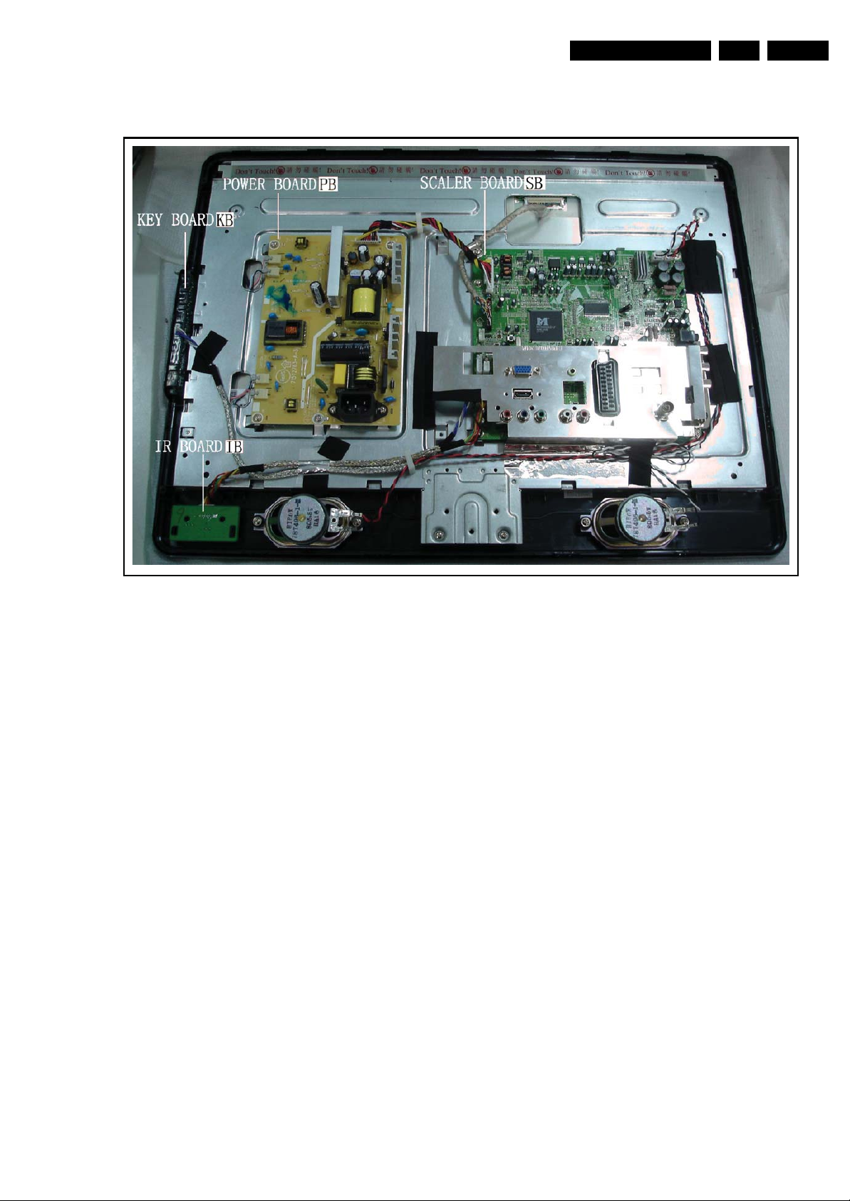
1.3 Chassis Overview
EN 3TPS1.4E LA 1.
Figure 1-3 Chassis Overview (22PFL3403)
I_17620_001.eps
250308
Page 4

EN 4 TPS1.4E LA2.
Safety Instructions, Warnings, and Notes
2. Safety Instructions, Warnings, and Notes
Index of this chapter:
2.1 Safety Instructions
2.2 Warnings
2.3 Notes
2.1 Safety Instructions
Safety regulations require the following during a repair:
• Connect the set to the Mains/AC Power via an isolation
transformer (> 800 VA).
• Replace safety components, indicated by the symbol h,
only by components identical to the original ones. Any
other component substitution (other than original type) may
increase risk of fire or electrical shock hazard.
Safety regulations require that after a repair, the set must be
returned in its original condition. Pay in particular attention to
the following points:
• Route the wire trees correctly and fix them with the
mounted cable clamps.
• Check the insulation of the Mains/AC Power lead for
external damage.
• Check the strain relief of the Mains/AC Power cord for
proper function.
• Check the electrical DC resistance between the Mains/AC
Power plug and the secondary side (only for sets that have
a Mains/AC Power isolated power supply):
1. Unplug the Mains/AC Power cord and connect a wire
between the two pins of the Mains/AC Power plug.
2. Set the Mains/AC Power switch to the "on" position
(keep the Mains/AC Power cord unplugged!).
3. Measure the resistance value between the pins of the
Mains/AC Power plug and the metal shielding of the
tuner or the aerial connection on the set. The reading
should be between 4.5 Mohm and 12 Mohm.
4. Switch "off" the set, and remove the wire between the
two pins of the Mains/AC Power plug.
• Check the cabinet for defects, to prevent touching of any
inner parts by the customer.
2.2 Warnings
• All ICs and many other semiconductors are susceptible to
electrostatic discharges (ESD w). Careless handling
during repair can reduce life drastically. Make sure that,
during repair, you are connected with the same potential as
the mass of the set by a wristband with resistance. Keep
components and tools also at this same potential. Available
ESD protection equipment:
– Complete kit ESD3 (small tablemat, wristband,
connection box, extension cable and earth cable) 4822
310 10671.
– Wristband tester 4822 344 13999.
• Be careful during measurements in the high voltage
section.
• Never replace modules or other components while the unit
is switched "on".
• When you align the set, use plastic rather than metal tools.
This will prevent any short circuits and the danger of a
circuit becoming unstable.
2.3 Notes
2.3.1 General
• Measure the voltages and waveforms with regard to the
chassis (= tuner) ground (H), or hot ground (I), depending
on the tested area of circuitry. The voltages and waveforms
shown in the diagrams are indicative. Measure them in the
Service Default Mode (see chapter 5) with a colour bar
signal and stereo sound (L: 3 kHz, R: 1 kHz unless stated
otherwise) and picture carrier at 475.25 MHz for PAL, or
61.25 MHz for NTSC (channel 3).
• Where necessary, measure the waveforms and voltages
with (D) and without (E) aerial signal. Measure the
voltages in the power supply section both in normal
operation (G) and in stand-by (F). These values are
indicated by means of the appropriate symbols.
2.3.2 Schematic Notes
• All resistor values are in ohms, and the value multiplier is
often used to indicate the decimal point location (e.g. 2K2
indicates 2.2 kohm).
• Resistor values with no multiplier may be indicated with
either an "E" or an "R" (e.g. 220E or 220R indicates 220
ohm).
• All capacitor values are given in micro-farads (μ= x10
nano-farads (n= x10
• Capacitor values may also use the value multiplier as the
decimal point indication (e.g. 2p2 indicates 2.2 pF).
• An "asterisk" (*) indicates component usage varies. Refer
to the diversity tables for the correct values.
• The correct component values are listed in the Spare Parts
List. Therefore, always check this list when there is any
doubt.
2.3.3 BGA (Ball Grid Array) ICs
Introduction
For more information on how to handle BGA devices, visit this
URL: www.atyourservice.ce.philips.com (needs subscription,
not available for all regions). After login, select “Magazine”,
then go to “Repair downloads”. Here you will find Information
on how to deal with BGA-ICs.
BGA Temperature Profiles
For BGA-ICs, you must use the correct temperature-profile,
which is coupled to the 12NC. For an overview of these profiles,
visit the website www.atyourservice.ce.philips.com (needs
subscription, but is not available for all regions)
You will find this and more technical information within the
"Magazine", chapter "Repair downloads".
For additional questions please contact your local repair help
desk.
2.3.4 Lead-free Soldering
Due to lead-free technology some rules have to be respected
by the workshop during a repair:
• Use only lead-free soldering tin Philips SAC305 with order
code 0622 149 00106. If lead-free solder paste is required,
please contact the manufacturer of your soldering
equipment. In general, use of solder paste within
workshops should be avoided because paste is not easy to
store and to handle.
• Use only adequate solder tools applicable for lead-free
soldering tin. The solder tool must be able:
– To reach a solder-tip temperature of at least 400°C.
– To stabilize the adjusted temperature at the solder-tip.
– To exchange solder-tips for different applications.
• Adjust your solder tool so that a temperature of around
360°C - 380°C is reached and stabilized at the solder joint.
Heating time of the solder-joint should not exceed ~ 4 sec.
Avoid temperatures above 400°C, otherwise wear-out of
tips will increase drastically and flux-fluid will be destroyed.
To avoid wear-out of tips, switch “off” unused equipment or
reduce heat.
-9
), or pico-farads (p= x10
-12
-6
),
).
Page 5

Directions for Use
EN 5TPS1.4E LA 3.
• Mix of lead-free soldering tin/parts with leaded soldering
tin/parts is possible but PHILIPS recommends strongly to
avoid mixed regimes. If this cannot be avoided, carefully
clear the solder-joint from old tin and re-solder with new tin.
2.3.5 Alternative BOM identification
The third digit in the serial number (example:
AG2B0335000001) indicates the number of the alternative
B.O.M. (Bill Of Materials) that has been used for producing the
specific TV set. In general, it is possible that the same TV
model on the market is produced with e.g. two different types
of displays, coming from two different suppliers. This will then
result in sets which have the same CTN (Commercial Type
Number; e.g. 28PW9515/12) but which have a different B.O.M.
number.
By looking at the third digit of the serial number, one can
identify which B.O.M. is used for the TV set he is working with.
If the third digit of the serial number contains the number “1”
(example: AG1B033500001), then the TV set has been
manufactured according to B.O.M. number 1. If the third digit is
a “2” (example: AG2B0335000001), then the set has been
produced according to B.O.M. no. 2. This is important for
ordering the correct spare parts!
For the third digit, the numbers 1...9 and the characters A...Z
can be used, so in total: 9 plus 26= 35 different B.O.M.s can be
indicated by the third digit of the serial number.
Identification: The bottom line of a type plate gives a 14-digit
serial number. Digits 1 and 2 refer to the production centre (e.g.
AG is Bruges), digit 3 refers to the B.O.M. code, digit 4 refers
to the Service version change code, digits 5 and 6 refer to the
production year, and digits 7 and 8 refer to production week (in
example below it is 2006 week 17). The 6 last digits contain the
serial number.
MODEL :
PROD.NO:
32PF9968/10
AG 1A0617 000001
MADE IN BELGIUM
220-240V 50/60Hz
~
VHF+S+H+UHF
S
128W
BJ3.0E LA
E_06532_024.eps
260308
Figure 2-1 Serial number (example)
2.3.6 Board Level Repair (BLR) or Component Level Repair (CLR)
If a board is defective, consult your repair procedure to decide
if the board has to be exchanged or if it should be repaired on
component level.
If your repair procedure says the board should be exchanged
completely, do not solder on the defective board. Otherwise, it
cannot be returned to the O.E.M. supplier for back charging!
2.3.7 Practical Service Precautions
• It makes sense to avoid exposure to electrical shock.
While some sources are expected to have a possible
dangerous impact, others of quite high potential are of
limited current and are sometimes held in less regard.
• Always respect voltages. While some may not be
dangerous in themselves, they can cause unexpected
reactions that are best avoided. Before reaching into a
powered TV set, it is best to test the high voltage insulation.
It is easy to do, and is a good service precaution.
3. Directions for Use
You can download this information from the following websites:
http://www.philips.com/support
http://www.p4c.philips.com
Page 6
EN 6 TPS1.4E LA4.
Mechanical Instructions
4. Mechanical Instructions
Index of this chapter:
4.1 Cable Dressing
4.2 Service Positions
4.3 Assy/Panel Removal
4.4 Set Re-assembly
4.1 Cable Dressing
Notes:
• Figures below can deviate slightly from the actual situation,
due to the different set executions.
• Follow the disassembly instructions in the described order.
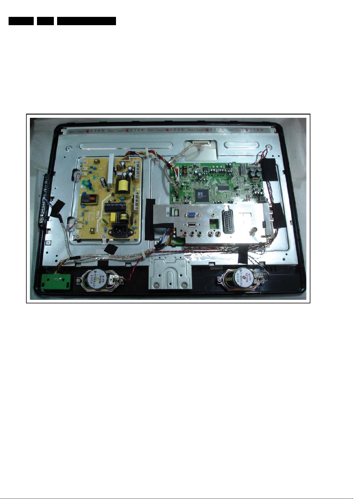
Figure 4-1 Cable dressing (22PFL3403)
I_17620_002.eps
250308
Page 7
Mechanical Instructions
EN 7TPS1.4E LA 4.
4.2 Service Positions
For easy servicing of this set, there are a few possibilities
created:
• The buffers from the packaging (see figure "Rear cover").
• Foam bars (created for Service).
4.2.1 Foam Bars
1
Required for sets
1
42"
E_06532_018.eps
171106
Figure 4-2 Foam bars
The foam bars (order code 3122 785 90580 for two pieces) can
be used for all types and sizes of Flat TVs. See figure “Foam
bars” for details. Sets with a display of 42” and larger, require
four foam bars [1]. Ensure that the foam bars are always
supporting the cabinet and never only the display. Caution:
Failure to follow these guidelines can seriously damage the
display!
By laying the TV face down on the (ESD protective) foam bars,
a stable situation is created to perform measurements and
alignments. By placing a mirror under the TV, you can monitor
the screen.
4.3 Assy/Panel Removal
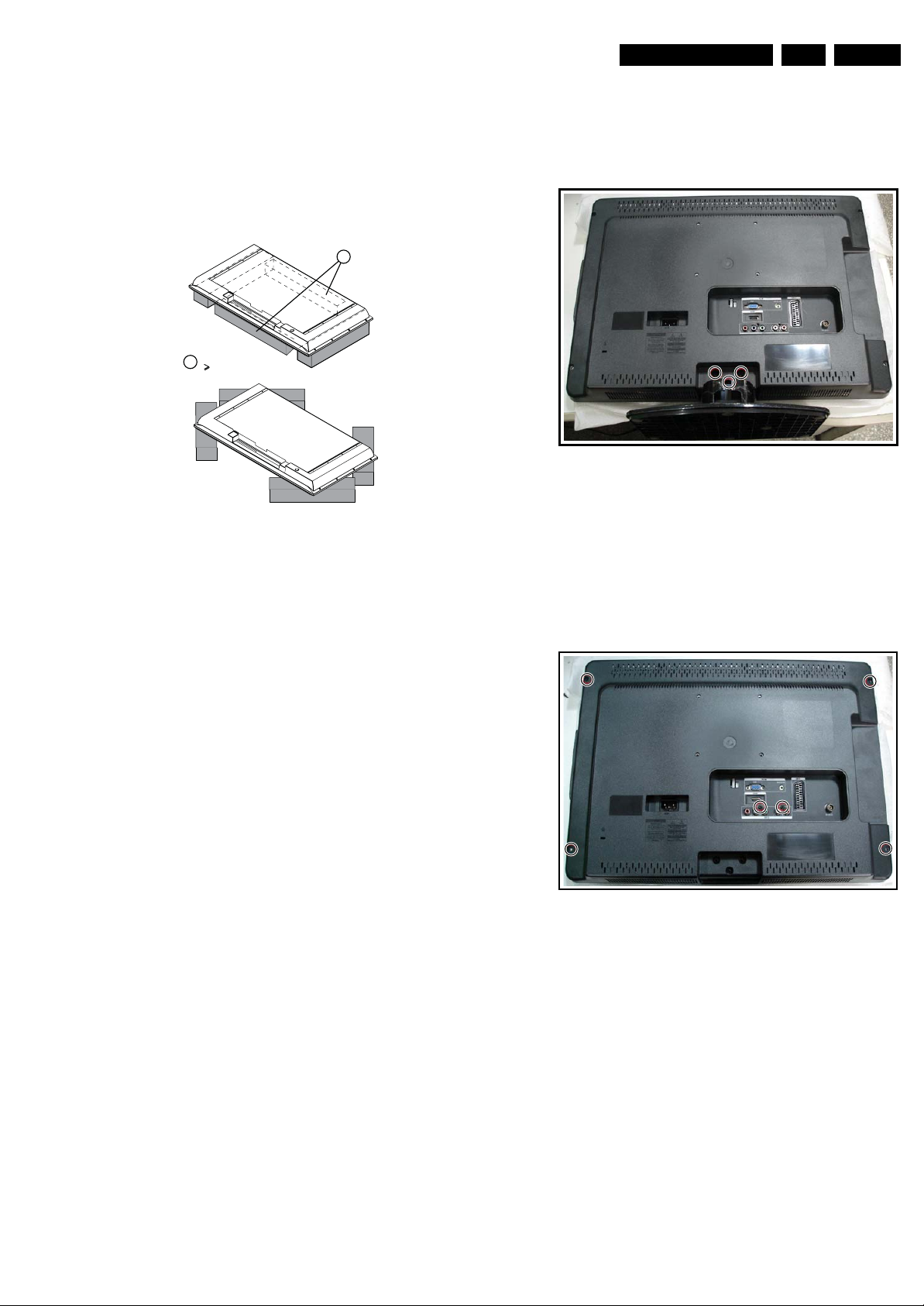
4.3.1 Stand Assy
Unscrew the marked screws to remove the stand assy.
Figure 4-3 Remove Stand ASSY
4.3.2 Rear Cover
1. Remove the six marked screws that secure the rear cover.
2. Pay attention to the internal hooks while removing the rear
cover. Use e.g. a plastic putty knife to release the hooks on
the bottom, the top, the left and the right side, then you can
easily remove the rear cover from the bezel.
I_17620_003.eps
250308
Figure 4-4 Remove Rear Cover
I_17620_004.eps
250308
Page 8
EN 8 TPS1.4E LA4.
Mechanical Instructions
4.3.3 Bezel
1. Refer to the next figure.
2. Unplug connector remarked in blue.
3. Release the marked screws and remove the bezel.
When defective, replace the whole unit.
Figure 4-5 Bezel
4.3.4 Shielding-EMI
1. Refer to next figure.
2. Release the marked screws and remove the shielding.
When defective, replace the whole unit.
I_17620_005.eps
250308
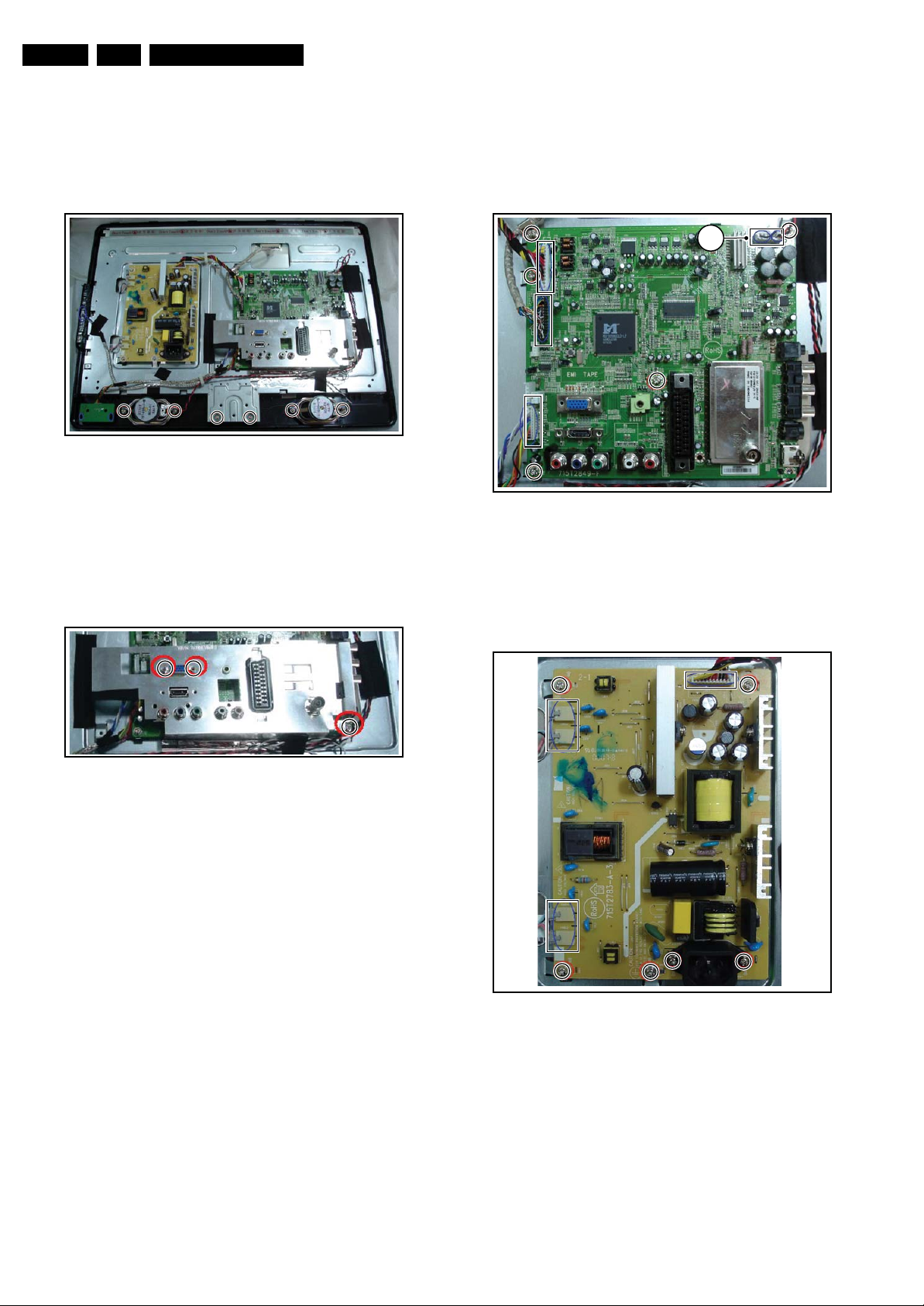
4.3.5 Main Board
1. Refer to next figure.
2. Unplug all connectors.
3. Remove the marked screws and then remove the main
board.
When defective, replace the whole unit.
(2x)
Figure 4-7 Main Board
4.3.6 Power Board
1. Refer to next figure. Unplug the connectors.
2. Unscrew the marked screws to remove the power board.
I_17620_007.eps
250308
Figure 4-6 EMI Shielding
I_17620_006.eps
250308
Figure 4-8 Power Board
I_17620_008.eps
250308
Page 9

4.3.7 Main Frame
1. Refer to next two figures.
2. Remove the marked screws.
Figure 4-9 Main Frame1
Figure 4-10 Main Frame2
4.4 Set Re-assembly
To re-assemble the whole set, execute all processes in reverse
order.
Mechanical Instructions
I_17620_009.eps
250308
I_17620_010.eps
250308
EN 9TPS1.4E LA 4.
Notes:
• While re-assembling, make sure that all cables are placed
and connected in their original position. See figure "Cable
dressing".
Page 10
EN 10 TPS1.4E LA5.
Service Modes, Error Codes, and Fault Finding
5. Service Modes, Error Codes, and Fault Finding
Index of this chapter:
5.1 Test Points
5.2 Service Mode
5.3 Service Tools
5.4 Tips and Tricks
5.1 Test Points
This chassis is NOT equipped with test points in the service
printing.
5.2 Service Mode
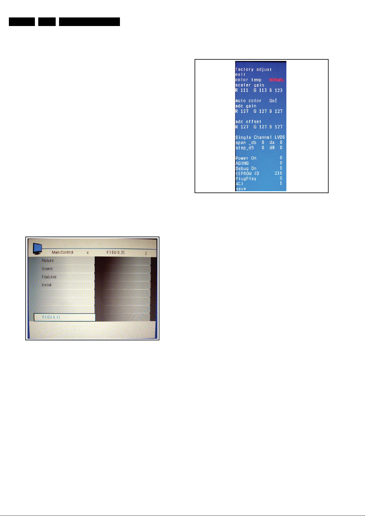
5.2.1 Factory Mode
How to Enter
To enter the Factory mode, use one of the following methods:
• Turn on the monitor, press the “menu” key.
• Press remote control code ”062596”, then press “Info [i+]”
key. When you press the “menu” key again, the OSD
will show as below, then you can just press the “F3 EU
0.21” to carry out the factory OSD. Caution: This
functions are avaible for development and service
personnel only, not for end customers.
After entering factory mode, the following screen is visible, the
values can be adjusted according to the requested.
How to EXIT
Choose ‘EXIT”, then press “OK” button on remote control.
Figure 5-2 Factory mode menu 2
I_17620_012.eps
250308
Figure 5-1 Factory mode menu 1
I_17620_011.eps
250308
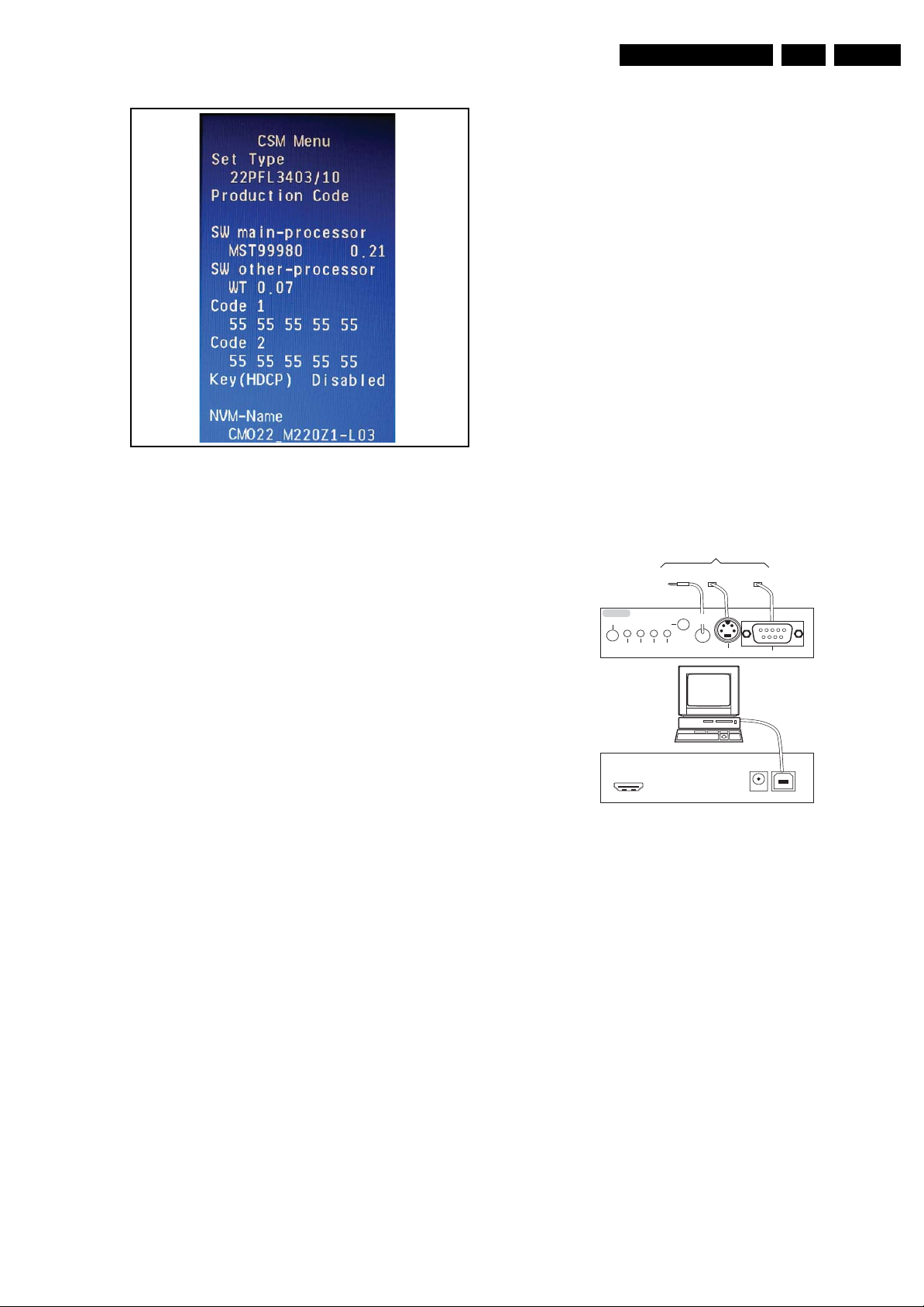
5.2.2 Customer Service Mode (CSM)
Purpose
When a customer is having problems with his TV-set, he can
call his dealer or the Customer Helpdesk. The service
technician can then ask the customer to activate the CSM, in
order to identify the status of the set. Now, the service
technician can judge the severity of the complaint. In many
cases, he can advise the customer how to solve the problem,
or he can decide if it is necessary to visit the customer. The
CSM is a read only mode; therefore, modifications in this mode
are not possible.
How to Activate CSM
Key in the code”123654” via the standard RC transmitter.
How to Navigate
By means of the “CURSOR-DOWN/UP” knob on the RCtransmitter on the screen.
Page 11
Service Modes, Error Codes, and Fault Finding
EN 11TPS1.4E LA 5.
Contents of CSM
I_17620_013.eps
250308
Figure 5-3 CSM Menu (22PFL3403)
Menu Explanation
1. Set Type: Type number and region.
2. Production code: Product serial no.
3. SW main-processor: SW-naming of Mstar/Trident, see
format in generic service document.
4. SW other-processor: if valid.
5. Code 1: Logging I2C error codes in NVM/EEPROM (5 last
logged errors).
6. Code 2: Logging I2C error codes in NVM/EEPROM (5 first
logged errors).
7. Key (HDCP): Indicates if the HDCP-key are valid.
8. NVM-Name: Indicates the used LCD panel type and region
(NVM content and main SW depend on the used LCD
panel).
How to exit
Press ”MENU” on the RC-transmitter.
5.3 Service Tools
5.3.1 ComPair
Introduction
ComPair (Computer Aided Repair) is a Service tool for Philips
Consumer Electronics products. and offers the following:
1. ComPair helps you to quickly get an understanding on how
to repair the chassis in a short and effective way.
2. ComPair allows very detailed diagnostics and is therefore
capable of accurately indicating problem areas. You do not
have to know anything about I
yourself, because ComPair takes care of this.
3. ComPair speeds up the repair time since it can
automatically communicate with the chassis (when the uP
is working) and all repair information is directly available.
4. ComPair features TV software upgrade possibilities.
Specifications
ComPair consists of a Windows based fault finding program
and an interface box between PC and the (defective) product.
The (new) ComPair II interface box is connected to the PC via
an USB cable. For the TV chassis, the ComPair interface box
and the TV communicate via a bi-directional cable via the
service connector(s).
How to Connect
This is described in the ComPair chassis fault finding database.
TO
UART SERVICE
I2C SERVICE
CONNECTOR
CONNECTOR
ComPair II
RC in
Optional
Switch
Power ModeLink/
Activity
HDMI
I
2
C only
RC out
Multi
function
2
TO TV
TO
TO
UART SERVICE
CONNECTOR
2
C
I
PC
ComPair II Developed by Philips Brugge
Optional power
5V DC
C or UART commands
RS232 /UART
E_06532_036.eps
150208
Figure 5-4 ComPair II interface connection
Caution: It is compulsory to connect the TV to the PC as
shown in the picture above (with the ComPair interface in
between), as the ComPair interface acts as a level shifter. If
one connects the TV directly to the PC (via UART), ICs will be
blown!
How to Order
ComPair II order codes:
• ComPair II interface: 3122 785 91020.
• For SW see Philips service website.
•ComPair I
2
C interface cable: 9965 100 09269.
Note: If you encounter any problems, contact your local
support desk.
Page 12
EN 12 TPS1.4E LA5.
5.4 Tips and Tricks
Below find some repair tips and tricks.
5.4.1 Soft Reset
When a consumer has forgotten his lock code, you can set the
TV back in Virgin mode by keying in the code”978450” via the
standard RC transmitter. The NVM is not erased.
The standard unlock code will then be “0711”.
5.4.2 Hard Reset (erase NVRAM)
A hard reset is executed by together pressing the “P+” and “V+”
buttons on the TV, while unplugging and replugging the mains
cord.
Note: By using this hard reset mode, the TV will be brought
back in Virgin mode, but also all customer settings will be
erased!
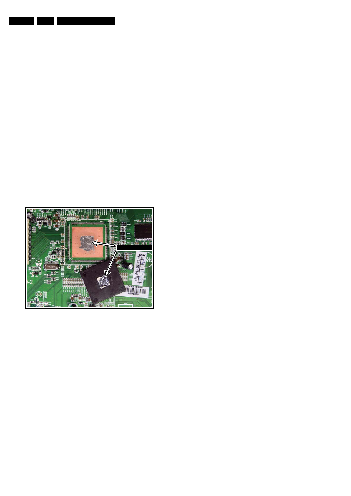
5.4.3 Removal of Morning Star Microprocessor
The Morning Star uP is fitted with a so-called E-pad (see photo
below). This is an extra surface for cooling and grounding. This
E-pad is soldered to the PWB.
To remove/place this IC on the PWB, use dedicated
equipment.
Service Modes, Error Codes, and Fault Finding
Soldered E-Pad
I_17620_046.eps
Figure 5-5 E-pad (photo from TPS1.0 chassis)
280308
Page 13
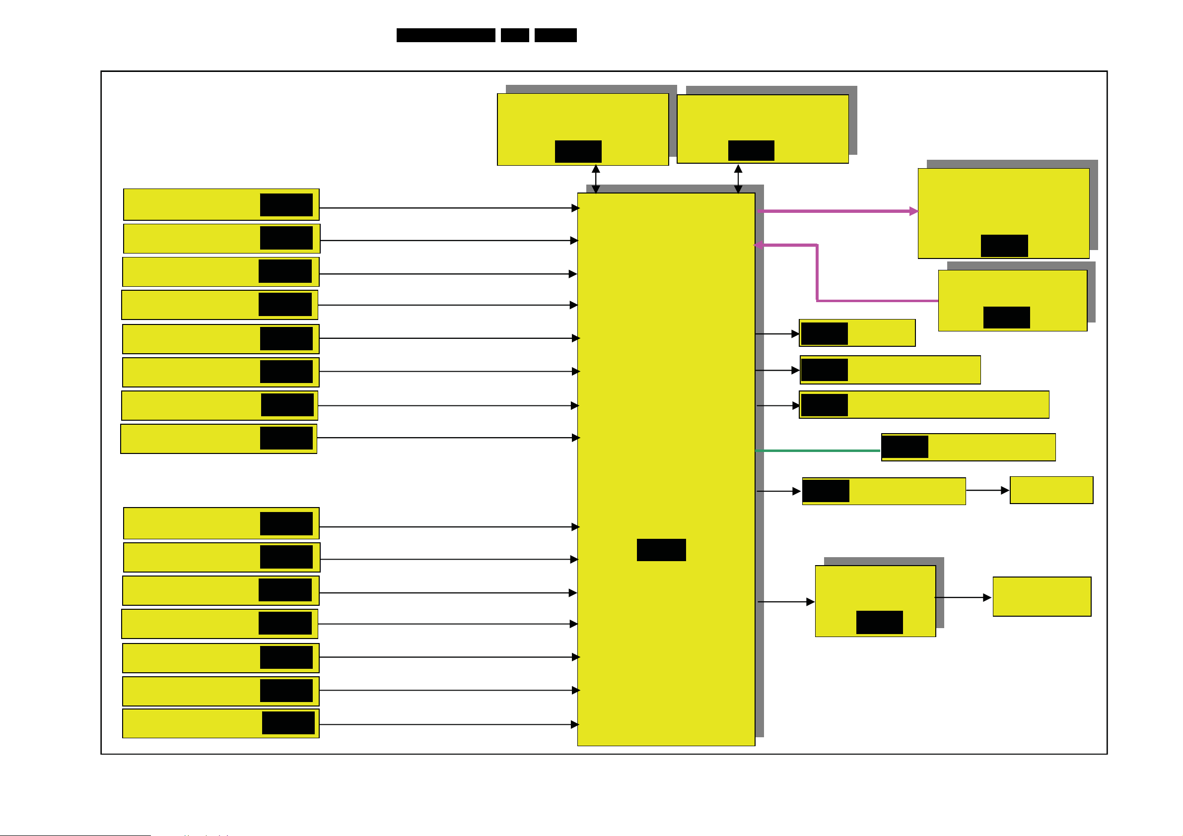
Block Diagrams, Test Point Overview, and Waveforms
6. Block Diagrams, Test Point Overview, and Waveforms
Wiring Diagram 22PFL3403
13TPS1.4E LA 6.
Key
Board
5 Pin
CN101
Panel
95T8013 3D 72
95T8013 2D 73
5
LVDS Cable
1
11
11 Pin
CN902
CN802
1
095T 82011D503
12
CN702
12 Pin
1
95T801830D168
3 Pin 2Pin
CN602
CN601
2131
30
CN801
CN108
30 Pin
MST99980CLD-LF
U401
Head Phone
Power Board
CN804
CN803
IR Board
AC IN
CN901
1
6 Pin
CN1
Main Board
VIDEO
1
AUDIO R/L
11
95T801411D 5
11Pin
S-VIDEO
CN401
HDMI
1
6
Speaker R/L
I_17620_014.eps
250308
Page 14
Block Diagrams, Test Point Overview, and Waveforms
Block Diagram Scaler Board 22PFL3403
PHILIPS 22W ATV Block Diagram
14TPS1.4E LA 6.
Video Block
Tuner PACK
CVI
S_VIDEO
VGA
HDMI 1
HDMI 2
SB-01
SB-02
SB-01
SB-03
SB-04
SB-04
Tuner_CVBS
YPbPr
Y/C
PC(R,G,B&H,V)
WT6702F_OG200WT
(MCU)
SB-10
EM638165TS-6G
SB-07
SB-06
SB-06
LVDS to panel
M220Z1-L03 CMO
SB-05
INVERTER POWER
SB-09
KEY/IR
IR Receiver LED
AV
SCART
HDMI-1
Audio Block
Tuner_SIF
CVI L/R
AVS_VIDEO L/R
PC AUDIO
HDMI 1
SB-01
SB-02
SB-01
SB-01
SB-01
SB-08
SB-04
CVBS
MST99980CLD
MST99980CLD
TV
TV
CONTROLLER
CONTROLLER
SB-06
SB-06
2
C BUS
I
SB-08
Flash MX25L8005M2I-15G
SB-05
EARPHONE AMP
YDA148
SB-08
EEPROM M24C32
speakers
Headphone
HDMI 2
SCART L/R
SB-04
SB-02
I_17620_015.eps
250308
Page 15
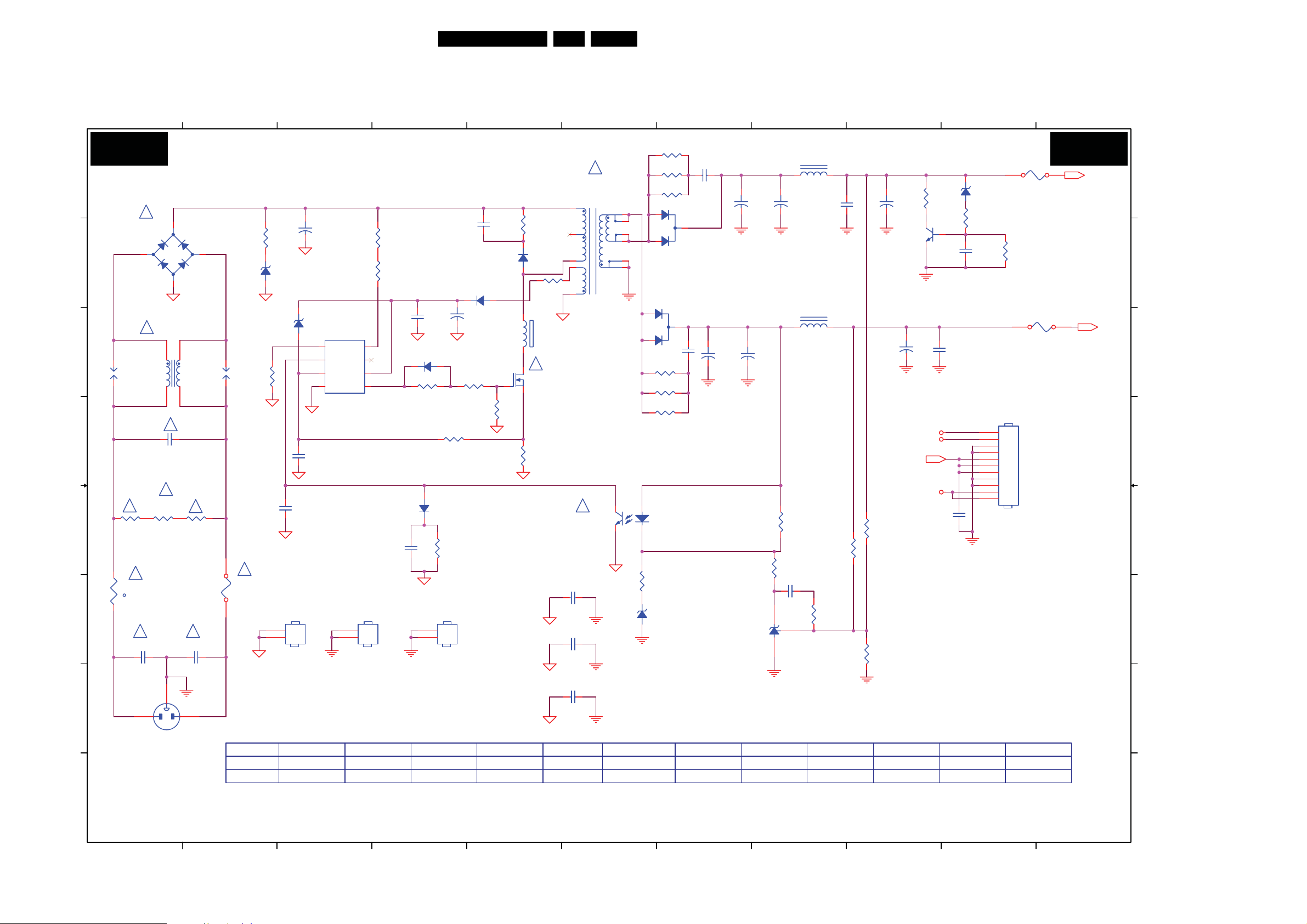
Circuit Diagrams and PWB Layouts
7. Circuit Diagrams and PWB Layouts
22PFL3403 Power Board Adapter
15TPS1.4E LA 7.
1
2
3
POWER BOARD: ADAPTER
PB01 PB01
A A
!
L902
!
L
73L 174 40LSG
C903
0.47UF
!
R902
620K 1/4W
1
+
-
4
1
4
SPARK GAP
2
3
!
!
R901
620K 1/4W
!
C902
0.001uF/250VAC
FG
3
12
2
SG902
R906
10R 1/4W
ZD903
P6KE440A
R941
100K 1/8W 1%
C923
470pF/25V
!
F901
FUSE
84G 56 4 B
ZD901
NC
HS1
HEAT SINK(Q901)
1
2
+
C905
120uF450VAC
67G315Z12115K
IC901
1
RT
2
COMP
3
CS
4
GND OUT
LD7575APS
56T 379107
C924
220pF
R904
8K2 1/4W
R905
8K2 1/4W
8
HV
7
NC
6
VCC
5
NC
HS2
HEAT SINK (D904)
1
2
BD901
GBU408
93G 50460900
3
B B
C C
SG901
SPARK GAP
D D
!
E E
F F
G G
R900
620K 1/4W
12
!
NR901
NTCR
61G 58 9T
t
!
C901
0.001uF/250VAC
C925
4
C919
0.1uF
D909
LL4148
R907
10R 1/8W
1
2
D910
NC
C906
2200pF 2KV
D902
FR103
93G 6038T52T
+
C908
22uF/50V
R912
10R 1/8W
R938
10K 1/8W
R922
200 1/8W
R931
NC
HS3
HEAT SINK(D906)
5
R908
100K 2W
D901
FR107
R909
3.3R 1/4W
12
FB901
Jumper
!
Q901
STP10NK70ZFP
57G 667 21
R914
0.36R 2W
T901
POWER X'FMR
80TL19T 33 N
4
5
6
3
2
!
IC903
PC123X2YFZOF
56G 139 3A
C931
0.001uF/250V
C907
NC
FG
C900
NC
FG
NC
8
L904
3.5uH
+
C918
L903
3.5uH
C920
0.1uF
9
+
C922
470uF/25V
PMBS3904
57G 417 4
C915
470uF/16V
Q903
+
R940
150R 2W
C916
0.1uF
6
R918
100R 1/4W
!
R919
7
C921
0.001uF
100R 1/4W
C914
+
C917
330uF/16V
+
C930
1000uF/16V
8
7
12
11
10
9
1
3
1
3
C929
0.001uF
R935
100R 1/4W
R903
R920
100R 1/4W
2
D906
YG865C15
93G 60268
D904
SP10100
93G 60267
2
+
1000uF/16V
10
ZD920
RLZ13B
R943
470R 1/8W
C932
0.001uF
F902
Jumper
R936
1K 1/4W
11
+12V
F903
+5V
Jumper
100R 1/4W
10
11
1
2
3
4
5
6
7
8
9
CN902
CONN
R934
100R 1/4W
12
43
R924
NC
R929
33K 1/8W 1%
DIM
ON/OFF
+5V
+12V
C927
0.1uF
R927
R937
NC
ZD902
NC
R925
150R 1/8W
IC902
KIA431VLA
56G 158 12
0.022uF/25V
C912
3K6 1/8W 1%
R928
0 1/8W
R930
2.43K 1/8W 1%
BD901 B1 CN901 G1
CN902 D10 C900 G6
C901 F1 C902 F2
C903 D1 C905 B3
C906 B5 C907 F6
C908 B4 C912 F8
C914 C7 C915 C9
C916 C9 C917 A7
C918 A8 C919 C4
C920 A8 C921 A7
C922 A9 C923 E2
C924 D3 C925 E4
C927 E10 C929 C7
C930 C7 C931 F6
C932 B10 D901 B5
D902 B4 D904 B6
D906 A6 D909 C4
D910 E4 FB901 C5
F901 E2 F902 A10
F903 C10 HS1 F3
HS2 F3 HS3 F4
IC901 C3 IC902 F8
IC903 E6 L902 C1
L903 C8 L904 A8
NR901 E1 Q901 C5
Q903 B9 R900 E1
R901 E2 R902 E1
R903 C6 R904 B3
R905 B3 R906 B2
R907 C4 R908 A5
R909 B5 R912 C4
R914 D5 R918 A6
R919 A6 R920 A6
R922 D4 R924 E8
R925 E8 R927 E8
R928 F8 R929 E9
R930 F9 R931 E4
R934 D6 R9
R936 B10 R937 E6
R938 C5 R940 A9
R941 C2 R943 A10
SG901 C1 SG902 C2
S4 F1 S5 F2
S6 E1 S7 E1
S8 D1 S9 E2
S10 E2 S11 D1
S12 C1 S14 A1
S15 C5 S16 E6
S17 A6 T901 A6
ZD901 C3 ZD902 F6
ZD903 B2 ZD920 A10
35 C6
CN901
SOCKET
H
1
MODE
22W ATV(12V)
22W DTV(16V)
2
ZD920
93G 39S 40 T
RLZ13B ROHM
93G 39S 44 T
RLZ18B
3
R929
61G0805330 2F
33K 1/8W 1%
61G0805430 2F
43K 1/8W 1%
T901
80TL19T 33 N
80TL22T 5 L
4
C917
67T 2043313KT
67G215S1024KV
5
C918
67G215S1024KV
C914 C930
NC 67T 2046
6
67G215S1023KV
812KT
7
D906
YG865C15RSC
93G 64 53 F
YG906C2RSC
86206 G39VK3201S512G76CN
H
I_17620_016.eps
8
9
10
250308
11
Page 16
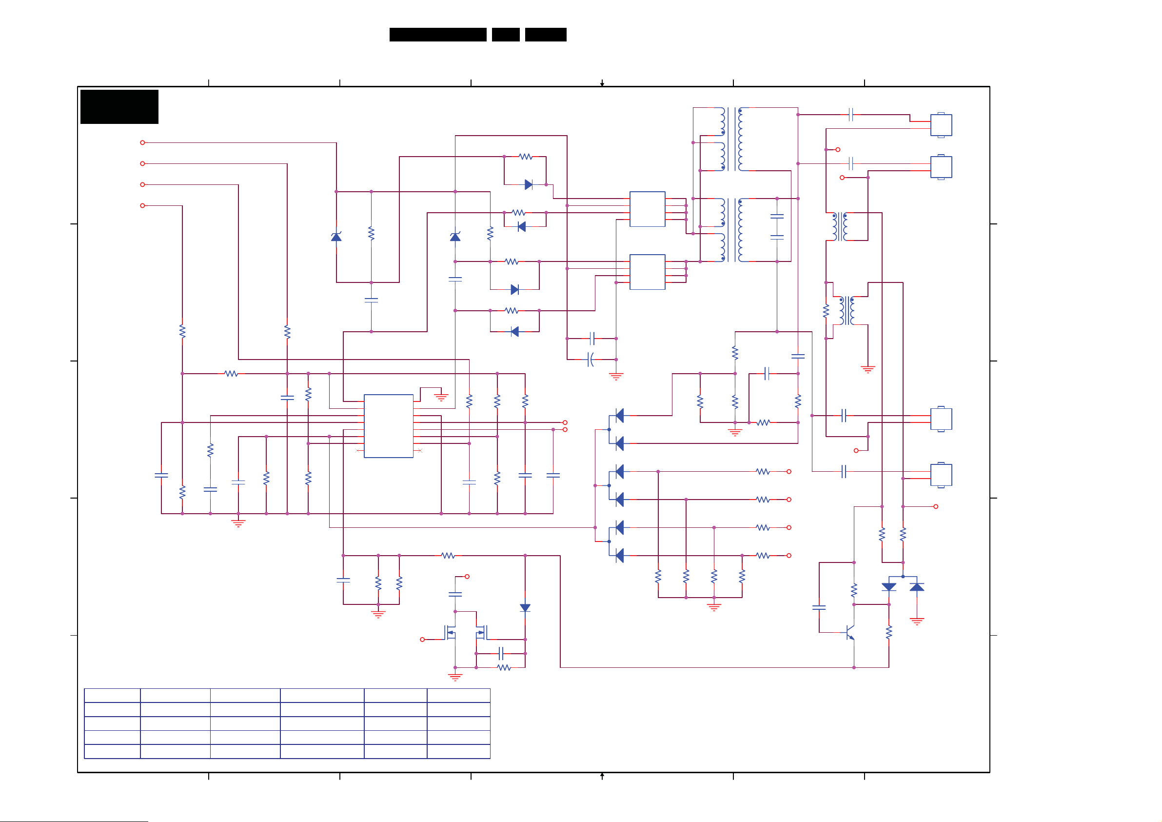
22PFL3403 Power Board Inverter
Circuit Diagrams and PWB Layouts
16TPS1.4E LA 7.
1
2
3
4
POWER BOARD: INVERTER
PB02
+12V
A A
5V
ON/OFF
DIM
ZD802
RLZ5.6B
R803
5K1 1/10W
1 2
ZD803
RLZ5.6B
1 2
C802
0.047uF
B B
R813
470K 1/10W
R814
NC
C806
1uF/16V
C
R816
10K 1/10W
C803
NC
D D
R815
NC
2.2uF/16V
C804
C805
0.01uF
R802
22R 1/8W
R817
1M 1/10W
R818
75K 1/10W
R819
100K 1/10W
C813
33NF
390R 1/10W 1%
C801
0.047uF
IC801
1
2
3
4
5
6
7
8 9
R823
PGND
DRV1
DRV2
VDDA
GNDA
TIMER
DIM
ISEN
VSEN
OVPT
NC1 NC2
OZ9938GN
56G 608 10
CT
SSTCMP
LCT
ENA
R824
3K9 1/10W 1%
SST
16
15
14
13
12
11
10
510R 1/10W
Q802
RK7002
R825
0.01uF
CT
C814
390PF
R820
10K 1/10W
C807
100R 1/10W
R806
100R 1/10W
R804
5K1 1/10W
R807
100R 1/10W
D803
LL4148
R808
100R 1/10W
D804
LL4148
R821
1M 1/10W
C808
180K 1/10W
Q803
RK7002
C815
0.047uF
R805
D801
LL4148
D802
LL4148
R822
20K 1/8W 1%
C809
560pF
D805
LL4148
CT
SST
C810
0.047uF
C811
0.1uF
+
C812
1000uF/25V
3
3
3
Q805
AO4616
4
G
3
S
2
G
1
S
57T 600517
Q806
4
G
3
S
2
G
1
S
AO4616
57T 600517
1
D806
BAV70
2
1
D807
BAV70
2
1
D808
BAV70
2
R842
10K 1/10W
D
D
D
D
D
D
D
D
5
5
6
7
8
5
6
7
8
R829
6K8 1/8W
POWER X'FMR
6
2
5
1
PT801
6
2
5
R828
6.2M 1/2W
R830
33K 1/8W
R843
10K 1/10W
PT802
NC
R844
10K 1/10W
20".22W
8
9
8
C816
27pF/6KV
C824
27pF/6KV
91
C817
2pF/6KV
C818
220pF
51K 1/10W
R837
6K8 1/10W
R838
1M 1/10W
R839
1M 1/10W
R840
1M 1/10W
R841
1M 1/10W
R845
10K 1/10W
?ࡁ
R836
LV 1
LV 2
LV 3
LV 4
6
R827
NC
LV 2
L801
1
2
L
L802
1
2
L
0R05 1/10W
C823
NC
C819
56pF/3KV
LV 1
C820
56pF/3KV
4
3
C821
56pF/3KV
LV 3
C822
56pF/3KV
Q804
NC
4
3
R846
R848
NC
R847
NC
3
2
R849
0R05 1/10W
1
2
1
2
1
2
1
2
D809
1
BAV99
7
CN801
CONN
CN803
CONN
CN804
CONN
LV 4
CN802
CONN
CN801 A7 CN802 A7
CN803 C7 CN804 C7
C801 B3 C802 B3
C803 C1 C804 C1
C805 C2 C806 C2
C807 C3 C808 C4
C809 C4 C810 C4
C811 B4 C812 B4
C813 D2 C814 D3
C815 E4 C816 A6
C817 B6 C818 C6
C819 A6 C820 A6
C821 C6 C822 C6
C823 D6 C824 B6
D801 A4 D802 A4
D803 B4 D804 B4
D
805 D4 D806 C4
D807 C4 D808 D4
D809 D7 IC801 C3
L801 A6 L802 B6
PT801 A5 PT802 A5
Q802 D3 Q803 D4
Q804 D6 Q805 A5
Q806 B5 R802 B2
R803 B3 R804 B4
R805 A4 R806 A4
R807 B4 R808 B4
R813 B1 R814 C2
R815 C1 R816 C1
R817 C2 R818 C2
R819 C2 R820 C3
R821 C4 R822 C4
R823
D3 R824 D3
R825 D3 R826 E4
R827 B6 R828 B5
R829 C5 R830 C5
R836 C6 R837 C6
R838 C6 R839 C6
R840 D6 R841 D6
R842 D5 R843 D5
R844 D5 R845 D5
C
R846 D7 R847 D7
R848 D6 R849 D7
ZD802 B2 ZD803 B3
R826
1M 1/10W
E E
MODE
22W ATV
22W DTV
PT801
NC
80GL20T 33 DN NC
1
PT802
80GL22T 4 DN
C819,C820,C821,C822 C816,C824
065G 3J5606ET
065G 3J6806ET
2
065G 3J2706ET
065G 3J2206ET
061G0603390 1F
061G0603620 1F
3
R824
I_17620_017.eps
4
5
6
7
250308
Page 17

Circuit Diagrams and PWB Layouts
17TPS1.4E LA 7.
22PFL3403 Layout Power Board (Top Side)
22PFL3403 Layout Power Board (Bottom Side)
I_17620_018.eps
250308
I_17620_019.eps
250308
Page 18

Scaler Board: Video Input
1
Circuit Diagrams and PWB Layouts
2
3
18TPS1.4E LA 7.
4
5
6
7
8
9
10
11
SB01 SB01
VIDEO INPUT
2
C161
0.1uF
TU101 TUNER
3
13
+5V
+5V IF
TH1
TH2
TH3
151617
18
C181 0.047uF
C174 0.047uF
C177
560pF
C180
560pF
V5A
CVBS
AF_O/P
SIFSND
AS_IF
TH4
FB108
300 OHM
2.2uF
C175
2.2uF
C178
+
C159
47uF/16V
V5C
N.C
N.C
N.C
C165
0.1uF
12
14
11
1
2
9
10
+
T1AF
T1SIF
VCOM1 8
CVBS1 8
AUL0_AV 8
AUR0_AV 8
+12V
L102
I2C_SCL8,12
I2C_SDA8,12
VCOM1_1
D119
VPORT0603100KV05
R187
27 OHM 2W
R188
33 OHM 2W
C160
C158
10UF16V
0.1uF
R192
10K OHM 1/10W
I2C_SCL
I2C_SDA
VCOM1_1
EMI
D117
D118
VPORT0603100KV05
VPORT0603100KV05
+
V5A
R208
C194
22pF
R211
10K OHM 1/10W
R213
10K OHM 1/10W
CN102
JACK
300 OHM
2
7
9
8
4
6
5
1
3
A
B B
C C
D D
E
3
1
C162
47uF/16V
R193
10K OHM 1/10W
R197
100 OHM 1/10W
R200
100 OHM 1/10W
0 OHM 1/8W
C176
22pF
C179
22pF
U103
AZ1117D-5.0-E1
OUTPUTINPUT
ADJ/GND
V5B
+
4
5
6
47 OHM 1/16W
AV1
47 OHM 1/16W
R210
75 OHM 1/8W
R212
12K OHM 1/10W
R214
12K OHM 1/10W
C164
0.1uF
SCL
SDA
AS_TU
EMI
FB107
300 OHM
R215
R209
L101
300 OHM
L103
300 OHM
C163
47uF/16V
V5B
V5C
R198
NC
R101
47 OHM 1/10W
C170
100pF
CN104
JACK
TV-CVBS
TV-CVBS
R204
1K OHM 1/10W
2
1
4
3
R191
NC
SIF
VPORT0603100KV05
D121
R201
NC
D120
VPORT0603100KV05
V5C
Q107
NC
R194
NC
75 OHM 1/8W
R222
10K OHM 1/10W
C189
22pF
R224
10K OHM 1/10W
C192
22pF
R189
0 OHM 1/10W
R202
SIF
12K OHM 1/10W
R225
12K OHM 1/10W
R223
0 OHM 1/8W
C168
680pF
R206NCC172
C190
560pF
C193
560pF
R195
22pF
C167
NC
C188
2.2uF
C191
2.2uF
R199
NC
R190
47 OHM 1/16W
R196
47 OHM 1/16W
R203
47 OHM 1/16W
R205
0 OHM 1/16W
R207
0 OHM 1/16W
AUL0_COM 8
AUR0_COM 8
C166
0.047uF
VCOM0
C169
0.047uF
C171
0.1uF25V
CLOSE to CHIP
C173
0.1uF25V
VIDEO_OUT 4
TUNER_CVBS8
VCOM0 8
SIFP0 8
SIFM0 8
CN102 D1 CN103 F1
CN104 D4 CN105 F7
C101 F4 C112 F4
C113 F4 C114 F4
C115 G3 C116 G3
C117 G4 C158 A2
C159 A3 C160 A1
A
C161 A3 C162 B2
C163 B3 C164 B3
C165 B3 C166 B8
C167 B6 C168 B6
C169 B8 C170 C4
C171 B8 C172 C6
C173 C8 C174 D3
C175 D3 C176 E2
C177 E3 C178 E3
C179 E2 C180 E3
C181 D3 C182 F10
C183 F6 C184 F7
C185 F8 C186 F9
C187 F6 C188 D7
C189 D5 C190 D6
C191 D7 C192 E5
C193 E6 C194 D2
D110 F2 D111 F2
D112 F2 D117 E2
D118 E1 D119 E1
D120 E5 D121 E5
D122 G7 D123 G8
FB107 C3 FB108
L101 A4 L102 A1
L103 A4 Q107 A5
R101 C4 R130 F4
R131 F4 R132 F4
R133 F4 R134 G3
R135 G3 R136 G3
R187 A2 R188 A2
R189 A5 R190 A7
R191 A5 R192 B2
R193 B2 R194 B5
R195 B6 R196 B7
R197 C2 R198 C4
R199 B7 R200 C2
R201 B5 R202 B6
R203 B7 R204 C4
R205 B7 R206 C6
R207 C7 R208 D2
R209 D2 R210 D2
R211 D2 R212 E2
R213 E2 R214 E2
R215 D2 R216 F6
R217 F8 R218 F9
R219 F6 R220 F9
R221 F6 R222 D5
R223 D6 R224 D5
R225 E6 TU101 B3
E
C3
F F
G G
H
CN103
JACK
Pr
Pb
Y
2
1
4
3
6
5
D110
AUDIO&VIDEO Input
1
VPORT0603100KV05
2
D111
D112
VPORT0603100KV05
VPORT0603100KV05
C182
0.047uF
SV_C0
SV_Y0
SV_C0 8
SV_Y0 8
C187
R221
C112
R130
R131
R132
R133
0.047uF
C113
0.047uF
C114
0.047uF
C101
0.001uF
47 OHM 1/10W
47 OHM 1/10W
47 OHM 1/10W
470 OHM 1/10W
C115
10pF
75 OHM 1/8W
R134
C116
10pF
75 OHM 1/8W
R135
C117
10pF
75 OHM 1/8W
R136
Y+ 8
PR+ 8
PB+ 8
SOY 8
47 OHM 1/16W
R219
75 OHM 1/8W
0.047uF
R216
47 OHM 1/16W
C183
NC
C184
47pF
CN105
4
2
6
DIN JACK
D122
VPORT0603100KV05
3
1
5
R217
47 OHM 1/16W
C185
47pF
D123
VPORT0603100KV05
C186
NC
S-LUM0
R220
75 OHM 1/8W
R218
47 OHM 1/16W
SV GND Reference to VCOM0
S-Video Input
I_17620_020.eps
3
4
5
6
7
8
9
10
250308
11
H
Page 19

Circuit Diagrams and PWB Layouts
19TPS1.4E LA 7.
Scaler Board: SCART & YPbPr
1
2
3
4
5
6
7
8
9
10
11
SCART & YPbPr
SB02 SB02
A A
3
C128
47pF
2
D115
BAV99
AUDIO_OUT_L
1
75 OHM 1/10W
1
2
1
D113
BAV99
CVBS INPUT
B B
C C
D
E
F F
Switch
C136
47pF
Blanking I/O
C137
47pF
CN106
SCART
20
18
16
14
12
10
8
6
4
2
10K OHM 1/10W
1.5K OHM 1/10W
75 OHM 1/8W
21
19
17
15
13
11
9
7
5
3
1
R158
R162
R163
3
Red I/O
Green I/O CVBS OUT
Blue I/O
Audio L-Input
SC_FS
SC_FS8
SC_FSW
SC_FSW 8
1
2
D114
BAV99
3
Audio R-Input
Audio L-Out
Audio R-Out
2
D116
BAV99
3
C122
47pF
R145
FB109
1
300 OHM
C131
0.001uF
FB110
1
300 OHM
C138
0.001uF
C146
0.001uF
AUDIO_OUT_R
C149
0.001uF
+5V
C123
47pF
100uF/16V
2
2
100 OHM 1/10W
R164
100K OHM 1/10W
100 OHM 1/10W
R173
100K OHM 1/10W
C124
47pF
C129
+
C132
NC
SCART_ARin1
C139
NC
R161
R168
C125
47pF
75 OHM 1/8W
R141
R148 10K OHM 1/10W
R154
10K OHM 1/10W
C144
4.7uF
LineMute
C151
4.7uF
LineMute10
LineMute
75 OHM 1/8W
75 OHM 1/8W
R142
R143
12K OHM 1/10W
12K OHM 1/10W
75 OHM 1/8W
R144
C133
560pF
R150
C141
560pF
R155
R167
4.7K OHM 1/10W
R169
4.7K OHM 1/10W
R180
4.7K OHM 1/10W
R184
47K OHM 1/10W
R137
47 OHM 1/16W
R138
47 OHM 1/16W
R139
47 OHM 1/16W
R140
47 OHM 1/16W
C130
2.2uF
CLOSE TO CHIP
C135
2.2uF
680 OHM 1/10W
Q105
R174
PMBS3904
100K OHM 1/10W
680 OHM 1/10W
Q106
100K OHM 1/10W
PMBS3904
R181
C118
0.047uF
C119
0.047uF
C120
0.047uF
C121
0.047uF
AUR1 8
AUL1 8
R165
R178
C145
4.7uF
R166
C152
4.7uF
R182
SC_CVBS
SCR+
SCG+
SCB+
NC
NC
SC_CVBS8
SCR+ 8
SCG+ 8
SCB+ 8
C134
0.1uF
+
C142
100uF/16V
R170
33K OHM 1/10W
C148
100pF
R185
33K OHM 1/10W
C157
100pF
TVOUT2
V8AUD
1
7
TV CVBS Output
R156
47K OHM 1/10W
R160
47K OHM 1/10W
R171
10K OHM 1/10W
R177
47K OHM 1/10W
10K OHM 1/10W
LM358D
4 8
U102
2
-
+
3
4.0V
5
+
-
6
R186
C143
1uF
R176
47K OHM 1/10W
C154
C153
1uF
2.2uF
+5V
FB105
600 OHM
VIDEO_OUT3
C147 4.7uF
close
to
audio
amp
C155 4.7uF
12
C126
0.1uF
R175
22K OHM 1/10W
R183
22K OHM 1/10W
C127
+
10UF16V
R151
10K OHM 1/16W
R152
NC
+
C140
10UF16V
R157
10K OHM 1/16W
R172
100 OHM 1/10W
C150
0.01uF
R179
100 OHM 1/10W
C156
0.01uF
2Vp-p
Q103
PMBS3906
R146
470 OHM 1/16W
Q104
PMBS3904
75 OHM 1/16W
Gainx2
75 OHM 1/16W
SCART OutL0 10
Placement Near
MST.IC DAC
output Pad
SCART OutR0 10
R149
R159
CN106 B1 C118 B6
C119 B6 C120 B6
C121 B6 C122 B3
C123 B3 C124 B4
C125 B4 C126 C9
C127 C9 C128 C3
C129 C4 C130 C5
C131 D3 C132 D3
C133 D5 C134 D7
C135 D5 C136 E1
C137 F1 C138 D3
C139 D3 C140 D9
C141 D5 C142 D6
C143 D8 C144 E4
C145 E6 C146 E3
C147 E8 C148 E6
C149 F3 C150 E9
C151 F4 C152 F6
C153 F8 C154 F8
C155 F8 C156 F9
C157 F6 D113 A2
D114 A2 D115 A2
D116 A3 FB105 C8
FB109 C3 FB110 D3
Q103 C10 Q104 D10
Q105 E5 Q106 F5
R137 B5 R138 B5
R139 B5 R140 B5
R141 B4 R142 B4
R143 B4 R144 B5
R145 C3 R146 C10
R14
8 C4 R149 D10
R150 D4 R151 D9
R152 D9 R154 D4
R155 D4 R156 D7
R157 D9 R158 E1
D
R159 D10 R160 D8
R161 E3 R162 E2
R163 F2 R164 E3
R165 E5 R166 E6
R167 E4 R168 F3
R169 E5 R170 E6
R171 E7 R172 E9
R173 F3 R174 E5
R175 E9 R176 E8
R177 F8 R178 F5
E
R179 F9 R180 F4
R181 F5 R182 F6
R183 F9 R184 F5
R185 F6 R186 F7
G G
H H
I_17620_021.eps
1
2
3
4
5
6
7
8
9
10
250308
11
Page 20

Circuit Diagrams and PWB Layouts
20TPS1.4E LA 7.
Scaler Board: VGA
1
2
3
4
5
VGA
SB03 SB03
CN107
1716
DB15
11
ZD106
TZMC5V6
ZD109
12
13
14
15
ZD107
TZMC5V6
VGA5V
A
B B
ZD108
TZMC5V6
C
+5V
EMI
D D
TZMC5V6
FB106 300 OHM
1
6
2
7
3
8
4
9
5
10
1
2
C195
0.1uF25V
VGA5V
D102
NC
D101
3
BAT54C
R831 0 OHM 1/16W
R832 0 OHM 1/16W
D104
D103
VPORT0603100KV05
VPORT0603100KV05
VGA_PW
DDC_SCL
C111
0.1uF25V
U101
1
A0
2
3
4 5
VCC
A1
WP
A2
SCL
VSS SDA
M24C02-WMN6TP
TXD 5,8,12
RXD 5,8,12
D105
VPORT0603100KV05
DDC_SDA
8
7
6
R128
R
G
B
R115
R114
75 OHM 1/8W
75 OHM 1/8W
R-
G-
B-
HSI
VSI
R122
R121
4.7K OHM 1/16W
4.7K OHM 1/16W
NC
R125
R126
100 OHM 1/16W
100 OHM 1/16W
R129
10K OHM 1/16W
R116
75 OHM 1/8W
R117
100 OHM 1/16W
R118
2.2K OHM 1/16W
100 OHM 1/16W
R120
2.2K OHM 1/16W
R123 NC
R124 NC
R127
NC
R11047 OHM 1/16W
R11147 OHM 1/16W
R11247 OHM 1/16W
R113
470 OHM 1/16W
HS_RGB
R119
VS_RGB
C196
22pF
EMI
RXD
TXD
C107 0.047uF
0.047uF
C108
C109 0.047uF
C110 1000pF
R833
0 OHM 1/8W
R834
0 OHM 1/8W
HS_RGB 8,12
VS_RGB 8,12
C197
22pF
RXD 5,8,12
TXD 5,8,12
RIN+ 8
GIN+ 8
BIN+ 8
SOG 8
A
C
CN107 A2
C107 A4
C108 A4
C109 A4
C110 A4
C111 C2
C195 D2
C196 C4
C197 C4
D101 C2
D102 A2
D103 A3
D104 A3
D105 A3
FB106 C1
R110 A4
R111 A4
R112 A4
R113 A4
R114 A3
R115 A3
R116 A4
R117 B4
R118 B4
R119 C4
R120 C4
R121 C3
R122 C3
R123 C4
R124 C4
R125 C3
R126 C3
R127 C3
R128 C3
R129 D3
R831 A2
R832 A2
R833 A4
R834 B4
U101 D2
ZD106 B1
ZD107 B1
ZD108 C1
ZD109 C1
I_17620_022.eps
250308
1
2
3
4
5
Page 21

Circuit Diagrams and PWB Layouts
21TPS1.4E LA 7.
Scaler Board: HDMI Input
1
SB04 SB04
HDMI INPUT
2
3
4
5
6
7
8
24C02=>EDID code must
HDMI-1
CN502
26
SHLD5
25
SHLD4
24
SHLD_GND2
SHLD_GND1
DDC_GND
CSHLD0
DSHLD2
DSHLD1
DSHLD0
TMDSC-
TMDSC+
TMDSD2-
TMDSD2+
TMDSD1-
TMDSD1+
TMDSD0-
TMDSD0+
HDMI
SHLD3
23
SHLD2
22
SHLD1
21
20
17
11
8
5
2
14
NC
18
VCC5
19
HPD
13
CEC
16
SDA
15
SCL
12
10
3
1
6
4
9
7
HDMI-2
HDMI_0C-
HDMI_02HDMI_02+
HDMI_01HDMI_01+
HDMI_00HDMI_00+
A A
B B
C C
HD5V1
EMI
R505
1K OHM 1/10W
DDC_CLK_IN1
DDC_DAT_IN1
CEC_INA
HPD1
D507
VPORT0603100KV05
D508
VPORT0603100KV05
1
2
L510 90 ohm
1
2
L511 90 ohm
1
2
L512 90 ohm
1
2
L513 90 ohm
C505
470pF
D509
VPORT0603100KV05
4
3
4
3
4
3
4
3
D510
VPORT0603100KV05
HDMI_RXC-_1
HDMI_RX2+_1
HDMI_RX2-_1
HDMI_RX1+_1
HDMI_RX1-_1
HDMI_RX0-_1
HDMI_RX0+_1
side
CN501
23
SHLD3
22
SHLD2
21
SHLD1
20
SHLD0
CSHLD0
DSHLD2
DSHLD1
DSHLD0
VCC5
HPD
CEC
SDA
SCL
TMDSC-
TMDSC+
17
11
8
5
2
14
NC
18
19
13
16
15
12
10
3
1
6
4
9
7
DDC_GND
D D
TMDSD2-
TMDSD2+
TMDSD1-
TMDSD1+
TMDSD0-
TMDSD0+
E
HDMI
HD5V2
R502
1K OHM 1/10W
DDC_CLK_IN2
DDC_DAT_IN2
HPD2
D503
D504
VPORT0603100KV05
VPORT0603100KV05
CEC_INB
D505
D506
VPORT0603100KV05
VPORT0603100KV05
be upto 256byte space,
for HDMI interface.
R508
R511
R510
47K OHM 1/16W
47K OHM 1/16W
100 OHM 1/16W
100 OHM 1/16W
DDC_SDA1
DDC_SCL1
1_+CXR_IMDH+C0_IMDH
10K OHM 1/16W
R514
R515
5
IN4 OUT4
4
IN3
2
IN2
1
IN1
U504 RClamp0524P.TCT
5
IN4 OUT4
4
IN3
2
IN2
1
IN1
U506 RClamp0524P.TCT
8
8
GND
GND
R509NC
3
OUT3
GND
OUT2
OUT1
3
OUT3
GND
OUT2
OUT1
24C02=>EDID code must
be upto 256byte space,
for HDMI interface.
R503
10K OHM 1/10W
R506
R507
47K OHM 1/10W
47K OHM 1/10W
R512
100 OHM 1/10W
100 OHM 1/10W
R513
DDC_SDA2
DDC_SCL2
HDMI_RXC-_3
HDMI_RX2-_3
HDMI_RX2+_3
HDMI_RX1-_3
HDMI_RX1+_3
HDMI_RX0-_3
HDMI_RX0+_3
HD_+5V1
U502
8
VCC
7
WP
6
SCL
R518
100 OHM 1/16W
100 OHM 1/16W
R504
NC
R516
100 OHM 1/10W
R517
100 OHM 1/10W
5
IN4 OUT4
4
IN3
2
IN2
1
IN1
U503 RClamp0524P.TCT
5 6
IN4 OUT4
4
IN3
2
IN2
1
IN1
U505 RClamp0524P.TCT
M24C02-WMN6TP
R519
Q502
PMBS3904
4.7K OHM 1/16W
6
7
9
10
6
7
9
10
U501
8
7
6
5
M24C02-WMN6TP
3
8
OUT3
GND
GND
OUT2
OUT1
3
8
OUT3
GND
GND
OUT2
OUT1
R521
VCC
WP
SCL
PMBS3904
R520
4.7K OHM 1/10W
GNDSDA
SDA_HD1
SCL_HD1
HD_+5V2
GNDSDA
Q501
HDMI_RX0+_3
6
HDMI_RX0-_3
7
HDMI_RXC+_3HDMI_RXC+_3
9
HDMI_RXC-_3
10
HDMI_RX2+_3
HDMI_RX2-_3
7
HDMI_RX1+_3
9
HDMI_RX1-_3
10
1
A0
2
A1
3
A2
45
SDA_HD1 8
SCL_HD1 8
HPLUGA 8
HDMI_RX0+_1 8
HDMI_RX0-_1 8
HDMI_RXC+_1 8
HDMI_RXC-_1 8
C502
0.1uF
1
A0
2
A1
3
A2
4
D501
BAT54C
3
C501
0.1uF
HDMI_RX2+_1 8
HDMI_RX2-_1 8
HDMI_RX1+_1 8
HDMI_RX1-_1 8
HD_+5V2
D502
BAT54C
3
EMI
C510
NC
R531 5R6 1/16W
R532 5R6 1/16W
R533 5R6 1/16W
R534 5R6 1/16W
R535 5R6 1/16W
R536 5R6 1/16W
R537 5R6 1/16W
R538 5R6 1/16W
C511
NC
1
2
1
2
C512
NC
HD5V1
HD5V2
R529
0 OHM 1/10W
EMI
+5V_STB
R530
0 OHM 1/10W
R539 22 OHM 1/16W
R541 22 OHM 1/16W
C513
NC
HDMI_000+_38
HDMI_000-_38
HDMI_00C+_38
HDMI_00C-_38
HDMI_002+_38
HDMI_002-_38
HDMI_001+_38
HDMI_001-_38
HD5V1+5V_STBHD_+5V1
CEC_INB
CEC_INA
C517
47pF
HD5V2
EMI
R522 0 OHM 1/10W
R523 0 OHM 1/10W
C516
47pF
C504
0.1uF25V
C514
EMI
120pF
R540 22 OHM 1/16W
R542 22 OHM 1/16W
HPLUGB 8
C515
470pF
EMI
C503
0.1uF25V
SDA_HD2 8
SCL_HD2 8
+5V_STB
R526
NC
Q503
RK7002
+3.3_SUB
R525
27K OHM 1/16W
R527
100 OHM 1/16W
ZD511
ZMM5V6
C518
0.1uF25V
R524
100 OHM 1/10W
EMI
R528
0 OHM 1/10W
EMI
C507
NC
C508
NC
To scaler
CEC
CEC 8
C506
NC
SUBCEC 12
C509
NC
CN501 C1 CN502 A1 C501 A4
C502 C4 C503 B6 C504 C5
C505 A2 C506 B8 C507 B8
C508 C8 C509 C8 C510 D4
C511 D5 C512 D5 C513 D5
C514 D6 C515 D6 C516 B5
C517 B5 C518 B7 D501 A4
D502 C4 D503 D2 D504 D2
D505 D2 D506 D3 D507 B2
D508 B2 D509 B2 D510 B3
L510 B2 L511 B2 L512 B2
L513 C2 Q501 D4 Q502 B4
Q503 B7 R502 C2 R503 C3
R504 C3 R505 A2 R506 C3
R507 C3 R508 A3 R509 A3
R510 A3 R511 A3 R512 D3
R513 D3 R514 A3 R515 A3
R516 D4 R517 D4 R518 B4
R519 B4 R520 D4 R521 B4
R522 B6 R523 B6 R524 B7
R525 B7 R526 B7 R527 B7
R528 C7 R529 A5 R530 C5
R531 D4 R532 D4 R533 D4
R534 D4 R535 E4 R536 E4
R537 E4 R538 E4 R539 D5
R540 D6 R541 D5 R542 D6
U501 C4 U502 A4 U503 D4
U504 B3 U505 E4 U506 B3
E
I_17620_023.eps
1
2
3
4
5
6
7
8
250308
Page 22

Scaler Board: Panel I/F
Circuit Diagrams and PWB Layouts
1
2
22TPS1.4E LA 7.
3
4
5
PANEL I/F
SB05 SB05
12V_SB
A A
+3.3_STB
Control port
+5V_STB
FB102 300 OHM
FB103 NC
FB104 NC
C104
1uF
R102
10K OHM 1/10W
R103
100K OHM 1/10W
R104
2K OHM 1/10W
C105
0.1uF
Q101
1
S
2
S
3
S
4
G
AM9435P-T1-PF
VPANEL
FB101
8
D
7
D
6
D
5
D
300 OHM
C103
0.1uF
+
C102
22uF/16V
CN108 C2
C102 A3
C103 A3
C104 A2
C105 A2
FB101 A3
FB102 A1
FB103 A1
FB104 A1
Q101 A2
Q102 B2
R102 A2
R103 B2
R104 B2
R105 B1
B B
PANPWR_ON8
R105
Q102
PMBS3904
4.7K OHM 1/10W
Panel Power
VPANEL
C C
RXE3+8
RXEC+8
RXE2+8
8
RXE1RXE0+8
RXO3+8
RXOC+8
RXO2-8
RXO1-8
8
RXO0-
D D
RXE2+
RXOC+
R
X
RXO0-
+3EXR+3EXR
+CEXR+CEXR
RXE2+
RXE1-RXE1RXE0+RXE0+
RXO3+-0EX
RXOC+
2OXR-2O
-
-1OXR-1OXR
RXO0-
29
27
25
23
21
19
17
15
13
11
9
7
5
3
1
CN108
CONN
8 bit LVDS
30
28
26
24
22
20
18
16
14
12
10
8
6
4
2
EXR
RXOC-
RXO0+
-3EXR-3
-CEXR-CEXR
RXE2-RXE2-
RXE1+RXE1+
-0EXR+3OXR
R
RXO3-RXO3-
RXOC-
RXO2+RXO2+
RXO1+RXO1+
RXO0+
RXE3- 8
RXEC- 8
RXE2- 8
RXE1+ 8
RXE0- 8
RXO3- 8
RXOC- 8
RXO2+ 8
RXO1+ 8
RXO0+ 8
I_17620_024.eps
250308
1
2
3
4
5
Page 23

Circuit Diagrams and PWB Layouts
23TPS1.4E LA 7.
Scaler Board: MST99980
1
2
3
4
5
6
7
8
9
10
11
MST99980
SB06 SB06
A
EMI
C451
C452
C453
470pF
B B
6
C C
D D
E
F F
G G
H
NC
NC
HDMI_RXC-_16
HDMI_RXC+_16
HDMI_RX0-_16
HDMI_RX0+_16
HDMI_RX1-_16
HDMI_RX1+_16
HDMI_RX2-_16
HDMI_RX2+_16
SDA_HD1
SCL_HD16
VIDEO INPUT
“ For CVBSOUT Application,please
refer to page6 (Video interface or
SCART interface)
SDA_HD1
SCL_HD1
HPLUGA
6
SDA_HD26
SCL_HD26
HPLUGB6
SC_CVBS4
SC_FSW
4
SCART INPUT
5
VGA
INPUT
3
3
3
3
Y, P b,Pr INPUT DVI/HDMI INPUT
TUNER_CVBS
3
HDMI_00C-_36
HDMI_00C+_36
HDMI_000-_36
HDMI_000+_36
HDMI_001-_36
HDMI_001+_36
HDMI_002-_36
HDMI_002+_36
SC_FS4
HS_RGB5,12
VS_RGB5,12
SV_C03
SV_Y03
VCOM1
CVBS13
VCOM03
SCB+4
SCG+4
SCR+4
BIN+5
SOG5
GIN+5
RIN+
PR+
SOY3
Y+
PB+
Close to chip
10UF16V
C413 1uF
C412 4.7uF
AUDIO INPUT
AUDI O
OUTPUT
I2C address
at A0.
U408
M24C32-WMN6TP
1
2
3
4
E0
E1E2WC
VSS
8
VCC
7
6
SCL
5
SDA
+5V_STB
HWRESET
12
HDMI_RXC-_1
HDMI_RXC+_1
HDMI_RX0-_1
HDMI_RX0+_1
HDMI_RX1-_1
HDMI_RX1+_1
HDMI_RX2-_1
HDMI_RX2+_1
R823 22 OHM 1/16W
R824 22 OHM 1/16W
HPLUGA
HDMI_00C-_3
HDMI_00C+_3
HDMI_000-_3
HDMI_000+_3
HDMI_001-_3
HDMI_001+_3
HDMI_002-_3
HDMI_002+_3
SDA_HD2
SCL_HD2
HPLUGB
SCB+
SCG+
SC_CVBS
SCR+
S
SC_FSW
HS_RGB
VS_RGB
BIN+
SOG
GIN+
RIN+
PR+
SOY
Y+
PB+
SV_C0
SV_Y0
VCOM1
CVBS1
TUNER_CVBS
VCOM0
+
0.1uF
C415
C414
+5V +5V
C422
0.1uF
VDDP
R830
SDA_HD11
SCL_HD11
C_FS
0 OHM 1/10W
R454
100 OHM 1/10W
R500
NC
SW401
SW
D401
LL4148
C454
NC
4
10
10
3
10
33 OHM 1/10W
33 OHM 1/10W
I2C_SDA3,12
I2C_SCL3,12
12
R455
4.7K OHM 1/10W
+
C401
10UF16V
R401
10K OHM 1/10W
EMI
C455
C456
NC
470pF
EMI
C404
0.1uF25V
C405
0.1uF25V
SC_CVBS
SIFP03
SIFM03
AUL0_ AV3
AUR0_AV3
AUL1
AUR14
R410
AUL2
AUR2
AUL0_COM
AUR0_COM3
NC
AUOutL310
AUOutR3
AUOutL110
AUOutR110
AUOutL010
AUOutR010
TXD5,12
RXD5,12
KEY1
KEY2
4.7K OHM 1/10W
I2C_SCL
I2C_SDA
U407
3
Vcc
NC/G690H293T73
Option
AVDDA
390 OHM 1/10W
NC
C450
NC
C406
NC
C409
0.1uF25V
C410
1000pF
R405 NC
R406 NC
R407 NC
R408 NC
R409 NC
R411
R412
R413
R414 22 OHM 1/10W
R415 22 OHM 1/10W
R471 22 OHM 1/10W
R416 22 OHM 1/10W
Mode Selection
+3.3_STB +3.3_STB+3.3_STB +3.3_STB
R417
10K OHM 1/10W
R421
NC
RESET
GND
HWRESET
C402
27PF J 50V NPO
C403
27PF J 50V NPO
R404
HPLUGA
C449
C408
0.1uF25V
SC_Chroma
SC_CVBS2
TUNER_CVBS
SIFP0
SIFM0
C411
0.1uF
KEY1
KEY2
R418
NC
PWM1PWM1 3MWP0MWP
R422
10K OHM 1/10W
2
1
X401
14.318MHZ
CL=20pF of XTAL
HDMI_RXC-_1
HDMI_RXC+_1
HDMI_RX0-_1
HDMI_RX0+_1
HDMI_RX1-_1
HDMI_RX1+_1
HDMI_RX2-_1
HDMI_RX2+_1
SDA_HD11
SCL_HD11
HDMI_00C-_3
HDMI_00C+_3
C448
470pF
HDMI_000-_3
HDMI_000+_3
HDMI_001-_3
HDMI_001+_3
HDMI_002-_3
HDMI_002+_3
HPLUGB
SDA_HD2
SCL_HD2
C407
0.1uF25V
PB+
Y+
SOY
PR+
SC_FS
SC_FSW
HS_RGB
VS_RGB
BIN+
SOG
GIN+
RIN+
SCB+
SOG1
SCG+
SCR+
SV_C0
SV_Y0
SC_CVBS
CVBS2
CVBS1
VCOM1
VCOM0
CVBSOut2
CVBSOut
AUVREF
AUVRA DP
AUVRADN
AUL0_ AV
AUR0_AV
AUL1
AUR1
AUCOM
AUL2
AUR2
AUL0_COM
AUR0_COM
AUMONO
AUOutL3
AUOutR3
AUOutL2
AUOutR2
AUOutL1
AUOutR1
AUOutL0
AUOutR0
R419
NC
PWM2PWM2
R423
LM810M3-2.93V
DIO/MA730
1
GND
R402
100 OHM 1/10W
9
RXACKN
10
RXACKP
12
RXA0N
13
RXA0P
15
RXA1N
16
RXA1P
18
RXA2N
19
RXA2P
20
HPLUGA
21
REXT
22
DDCDA_DA
23
DDCDA_CK
252
RXBCKN
253
RXBCKP
255
RXB0N
256
RXB0P
1
RXB1N
2
RXB1P
4
RXB2N
5
RXB2P
6
HPLUGB
7
DDCDB_DA
8
DDCDB_CK
26
VCLAMP
27
REFP
28
REFM
33
VCOM3
35
VCOM2
34
BIN0P
36
GIN0P
37
SOGIN0
38
RIN0P
41
HSYNC0
42
VSYNC0
24
HSYNC1
25
VSYNC1
29
BIN1P
30
SOGIN1
31
GIN1P
32
RIN1P
43
VSYNC2
44
BIN2P
45
SOGIN2
46
GIN2P
47
RIN2P
48
C1
49
Y1
50
C0
51
Y0
52
CVBS3
53
CVBS2
54
CVBS1
55
VCOM1
56
CVBS0
57
VCOM0
59
CVBSOUT1
60
CVBSOUT0
62
SIF0P
64
SIF1P
65
SIFM
69
AUVREF
68
AUVRADP
67
AUVRA DN
71
AUL0
72
AUR0
73
AUL1
74
AUR1
75
AUCOM
76
AUL2
77
AUR2
78
AUL3
79
AUR3
80
AUMONO
81
AUOUTL3
82
AUOUTR3
83
AUOUTL2
84
AUOUTR2
85
AUOUTL1
86
AUOUTR1
87
AUOUTL0
88
AUOUTR0
177
DDCR_DA
178
DDCR_CK
179
DDCA_DA
180
DDCA_CK
171
SAR0
172
SAR1
173
SAR2
174
SAR3
BL_ADJ11
10K OHM 1/10W
3
VCC
2
RESET
R403
1M OHM 1/10W
250
XIN
R420
10K OHM 1/10W
R424
NC
AVDD_AU
AVDD _SIF
248
249
70
XOUT
HWRESET
PWM0/MCUCFG0
PWM1/MCUCFG1
PWM2/MCUCFG2
175
176
192
191
PWM1
PWM2
PWM3
PWM0
“ +3.3V for AVDD_MPLL / AVDD_MemPLL / VDDP
/AVDD_ADC / AVDD_DVI / AVDD_SIF / AVDD_AU
“ +2.5V for VDDM
“ +1.2V for VDDC
VCC1.2V
AVDDA
14
39
58
101
149
165
99
185
193
254
63
AVDD _33
AVDD _33
AVDD _33
AVDD _AU
AVDD _SIF
240
VDDP
VDDP
VDDC
VDDC
VDDC
VDDC
VDDC
AVDD _33
VDDP
183
VDDP
194
207
VDDP
221
VDDP
235
VDDP
VDDP
108
VDDM
114
VDDM
U401
MST99980CLD-LF
PWM3/MCUCFG3
181
R487NC
REMOTE_OUT
INT
IRIN
167
182
SPI_CK
R425
22 OHM 1/10W
REMOTE_IN
+3.3_STB
SCK
SDI
SCZ
SDO
168
169
170
SPI_DO
SPI_DI
SPI_CZ
10K OHM 1/10W
SPI_CZ
SPI_DO
R428
GND
GND
GND
GND
3
11
17
40
R426
100 OHM 1/10W
R427
100 OHM 1/10W
61
GND
R429
NC
GND
GND
100
66
GND
GND
GND
GND
105
113
134
166
148
U404
1
CS#
2
SO
3
W#
4
GND
MX25L8005M2I-15G
AVDD_MemPLL
119
135
147
VDDM
VDDM
VDDM
VDDM
GND
GND
GND
GND
GND
184
208
222
241
+3.3_STB
C416
0.1uF
VCC
HOLD#
SCK
SI
AVDD_MPLL
136
AVDD_MEMPLL
GPIOB[4]/UART1_RX
186
8
7
6
330 OHM 1/10W
5
100 OHM 1/10W
EMI
251
AVDD_MPLL
GPIOB[5]/UART1_TX
GPIOB[6]
187
188
C457
10pF
89909192939495
GPIOF[0]
GPIOF[1]
GPIOF[2]
GPIOF[3]
AD[1]
AD[2]
AD[3]
AD[4]
AD[0]
155
156
157
158
154
R433
0 OHM 1/10W
R434
0 OHM 1/10W
R430
R431
96
97
GPIOF[4]
GPIOF[5]
GPIOF[6]
GPIOF[7]
LVSYNC/GPIOE[0]
LVH SYNC/GPIOE[1]
AD[5]
AD[6]
AD[7]
WRZ
159
160
161
163
162
R473 NC
R474 NC
4.7K OHM 1/10W
FB405
120 OHM
EMI
1 2
SPI_DI
98
189
190
NC
NC
GPIOF[9]
GPIOF[8]
DI[13]
DI[12]
DI[11]
DI[10]
DI[9]
DI[8]
DI[7]
DI[6]
DI[5]
DI[4]
DI[3]
DI[2]
DI[1]
DI[0]
IVSYNC
IHSYNC
IDE
ICLK
LDE/GPIOE[2]
LCK/GPIOE[3]
LVB 0M
LVB 0P
LVB 1M
LVB 1P
LVB 2M
LVB 2P
LVB CK M
LVB CK P
LVB 3M
LVB 3P
NC
NC
LVA0M
LVA0 P
LVA1 M
LVA1 P
LVA2 M
LVA2 P
LVACKM
LVACKP
LVA3M
LVA3P
NC
NC
MDATA[0]
MDATA[1]
MDATA[2]
MDATA[3]
MDATA[4]
MDATA[5]
MDATA[6]
MDATA[7]
MDATA[8]
MDATA[9]
MDATA[10]
MDATA[11]
MDATA[12]
MDATA[13]
MDATA[14]
MDATA[15]
MCLK
MCLKZ
MCLKE
MVREF
UDQM
LDQM
DQS[0]
DQS[1]
RASZ
CASZ
WEZ
BARD[1]
BARD[0]
MADR[11]
MADR[10]
MADR[9]
MADR[8]
MADR[7]
MADR[6]
MADR[5]
MADR[4]
MADR[3]
MADR[2]
MADR[1]
MADR[0]
RDZ
ALE
164
P42
0 OHM 1/10W
P41
R493 0 OHM 1/10W
R432
INVPRO
SPI_CK
247
246
245
244
243
242
239
238
237
236
234
233
232
231
230
229
228
227
226
225
224
223
220
219
218
217
216
215
214
213
212
211
210
209
206
205
204
203
202
201
200
199
198
197
196
195
MDATA0
123
MDATA1
122
MDATA2
121
MDATA3
120
MDATA4
118
MDATA5
117
MDATA6
116
MDATA7
115
MDATA8
112
MDATA9
111
MDATA10
110
MDATA11
109
MDATA12
107
MDATA13
106
MDATA14
104
MDATA15
103
130
MCLKZ
129
CKE
128
MVREF
127
UDQM
126
LDQM
125
DQS0
124
DQS1
102
RASZ
133
CASZ
137
WEZ
138
BA1
131
BA0
132
MADR11
153
MADR10
152
MADR9
151
MADR8
150
MADR7
146
MADR6
145
MADR5
144
MADR4
143
MADR3
142
MADR2
141
MADR1
140
MADR0
139
R436NC
R437NC
R438NC
R435
CEC 6
TURN_ON 12
STANDBY 12
INVPRO 11
AUDIO-RESET 10
RXO0-
RXO0+
RXO1-
RXO1+
RXO2RXO2+
RXOC-
RXOC+
RXO3-
RXO3+
RXE0RXE0+
RXE1RXE1+
RXE2RXE2+
RXEC-
RXEC+
RXE3-
RXE3+
100 OHM 1/10W
PAN P WR _ O N
MUTE
PWR_ON
33 OHM +-5% 1/16W
RP401
4
5
3
6
2
7
1
8
R450 33 OHM 1/16W
R451 33 OHM 1/16W
R452 33 OHM 1/16W
R45333 OHM 1/16W
R498
C459
NC
MDATA[0..15]
MADR[0..11]
+3.3_STB
PANPWR_ON 7
MUTE 10
SDRAM_ON 11
+3.3_STB
MCLK
RXO0- 7
RXO0+ 7
RXO1- 7
RXO1+ 7
RXO2- 7
RXO2+ 7
RXOC- 7
RXOC+ 7
RXO3-7
RXO3+7
RXE0- 7
RXE0+ 7
RXE1- 7
RXE1+ 7
RXE2- 7
RXE2+ 7
RXEC- 7
RXEC+ 7
RXE3-7
RXE3+7
Memory
INTERFACE
MDATA[0..15] 9
MCLK 9
MCLKZ 9
CKE 9
UDQM 9
LDQM 9
DQS09
DQS19
RASZ9
CASZ9
WEZ 9
BA1 9
BA0 9
MADR[0..11] 9
PANEL
INTERFACE
R/B SWAP
for TTL
VDDM
R440
10K OHM 1/10W
C417
0.001uF
R441
10K OHM 1/10W
C418
0.1uF
TURN_ON12
STANDBY
12
REMOTE_IN
12
+3.3_SUB
REMOTE_OUT
+3.3_SUB
KEY112
KEY2
DDCA_CK-->UART0_RX;
1
DDCA_DA-->UART0_TX
ICLK-->UART_RX0;
2
IDE-->UART_TX0
AD[7]-->UART_RX0;
3
WRZ-->UART_TX0
UART0 option table
+3.3_SUB +3.3_SUB
NC
R442
R443
NC
R444
0 OHM 1/10W
R445
0 OHM 1/10W
EMI
C446
1000pF
REMOTE_OUT
MAIN BOARD
C420
NC
R826
4.7K OHM 1/10W
TXD
RXD
R811 0 OHM 1/10W
R812 0 OHM 1/10W
C447
1000pF
R446
100 OHM 1/16W
R447
100 OHM 1/16W
C421
NC/4.7uF/10V
47K OHM 1/16W
OTS
+3.3_SUB
+3.3_SUB
REMOTE_IN
TXD
RXD
+5V_STB
+3.3_SUB
R825
4.7K OHM 1/10W
R827
100 OHM 1/10W
Keypad / IR Connector
Connect to Keypad
Board
Q401
NC
Q402
NC
C419
4.7uF/10V
EMI
C445
R449
47K OHM 1/16W
0.1uF25V
R448
R819NC
R820NC
Debug port
with
UART0
0 OHM 1/16W
R488
ZD404
ZD401
ZD403
ZD402
NC
R828
100 OHM 1/10W
ZD406
TZMC5V6
TZMC5V6
TZMC5V6
TZMC5V6
ZD405
TZMC5V6
1
2
3
4
5
6
7
8
9
10
11
CN401
CONN
D402
D403
VPORT0603100KV05
VPORT0603100KV05
CN402
1
2
3
4
5
CONN
CN404
1
2
3
CONN
CN401 B11 CN402 D10
CN404 E10 C401 A2
C402 A2 C403 B2
C404 C2 C405 C2
C406 C2 C407 C3
C408 C2 C409 C2
C410 D2 C411 E2
C412 E1 C413 E1
C414 E1 C415 E1
C416 G5 C417 E8
C418 E8 C419 B10
C420 B9 C421 B9
C422 F1 C445 C10
C446 B9 C447 B9
A
C448 B2 C449 C2
C450 C2 C451 A1
C452 A1 C453 A1
C454 B2 C455 B2
C456 B2 C457 H5
C459 G6 D401 A2
D402 B11 D403 B10
FB405 G5 Q401 A10
Q402 A10 RP401 B7
R401 A2 R402 A3
R403 A3 R404 B2
R405 D2 R406 D2
R407 D2 R408 E2
R409 E2 R410 E2
R411 E2 R412 F2
R413 F2 R414 F2
R415 F2 R416 F2
R417 G2 R418 G2
R419 G3 R420 G3
R421 H2 R422 H2
R423 H3 R424 H3
R425 G3 R426 G4
R427 G4 R428 G4
R429 H4 R430 G5
R431 H5 R432 G6
R433 G5 R434 G5
R435 G6 R436 F6
R437 F6 R438 G6
R440 E8 R441 E
R442 A9 R443 A9
R444 A9 R445 A9
R446 B9 R447 B9
R448 B10 R449 B10
R450 C7 R451 C7
R452 C7 R453 C7
R454 F2 R455 F2
R471 F2 R473 G5
R474 G5 R487 G3
R488 D10 R493 G6
R498 E7 R500 A2
R811 A9 R812 A10
R819 C10 R820 C10
R823 B1 R824 B1
R825 E9 R826 E9
R827 E10 R828 E10
R830 A2 SW401 A2
U401 B3 U404 G4
U407 A2 U408 G1
X401 A3 ZD401 D10
ZD402 D10 ZD403 D10
ZD404 D10 ZD405 E10
E
H
8
I_17620_025.eps
1
2
3
4
5
6
7
8
9
10
250308
11
Page 24

Scaler Board: DDR & SDRAM
1
Circuit Diagrams and PWB Layouts
2
24TPS1.4E LA 7.
3
4
5
6
7
8
SB07 SB07
MADR0
RP406 100 OHM +-5% 1/16W
MADR1
C432
0.1uF
C428
NC
MADR2
MADR3
MADR4
MADR5
MADR6
MADR7
MADR8
MADR9
MADR10
MADR11
C433
0.1uF
MVREF-D
C429
NC
WEZ
CASZ
RASZ
DQS1
DQS0
BA0
BA1
MCLK+
MCLK-
8
8
8
8
C431
0.1uF
R457
NC
MADR[0..11]
WEZ
CASZ
RASZ
DQS1
DQS08
UDQM8
LDQM8
BA08
BA18
MCLK8
MCLKZ8
8
MADR[0..11]
A A
B
DMC DMQ
C430
0.1uF
C C
+3.3MVDD
R456
NC
D D
8
7
6
5
RP407 100 OHM +-5% 1/16W
8
7
6
5
RP408 100 OHM +-5% 1/16W
8
7
6
5
R458 22 OHM 1/10W
R459 22 OHM 1/10W
R460 22 OHM 1/10W
R461 56 OHM 1/10W
R462 56 OHM 1/10W
R463 56 OHM 1/10W
R464 56 OHM 1/10W
C434
0.1uF
+3.3MVDD11
C435
0.1uF
1
2
3
4
1
2
3
4
1
2
3
4
C437
C436
0.1uF
0.1uF
ADR1
ADR2
ADR3 MDATA11
ADR4
ADR5
ADR6
ADR7
ADR8
ADR9
ADR10
ADR11 MDATA2
WEZM
CASZM
RASZM
DQML
DQMU
+3.3MVDD DMC
600 OHM
C424
2.2uF
2M X 16bit X 4BK
U402 NC/DDR_128Mb_TSOP66
29
A0
30
A1
31
A2
32
A3
35
A4
36
A5
37
A6
38
A7
39
A8
40
A9
28
A10/AP
41
A11
21
WE
22
CAS
23
RAS
16
LDQS
51
UDQS
20
LDM
47
UDM
26
BA0
27
BA1
24
CS
14
NC
17
NC
34
VSS
48
VSS
66
VSS
6
VSSQ
12
VSSQ
52
VSSQ
58
VSSQ
64
VSSQ
L401
C425
0.1uF
FB402
600 OHM
FB403
600 OHM
DQ0
DQ1
DQ2
DQ3
DQ4
DQ5
DQ6
DQ7
DQ8
DQ9
DQ10
DQ11
DQ12
DQ13
DQ14
DQ15
VREF
CLK
CLK
CKE
NC
NC
NC
NC
NC
NC
MVDD
MVDD
MVDD
VDDQ
VDDQ
VDDQ
VDDQ
VDDQ
DMQ
2
4
5
7
8
10
11
13
54
56
57
59
60
62
63
65
49
46
45
44
19
25
42
43
50
53
1
18
33
3
9
15
55
61
C426
0.1uF
C427
0.1uF
DATA8ADR0
RP402 100 OHM +-5% 1/16W
DATA9
DATA1 0
DATA1 1
DATA1 2
DATA1 3
DATA1 4
DATA1 5
DATA0
DATA1
DATA2
DATA3
DATA 4
DATA 5
DATA6
DATA7
MCLK-
MCLK+
CLK
256M
DMC DMQ
8
7
6
5
RP403 100 OHM +-5% 1/16W
8
7
6
5
RP404 100 OHM +-5% 1/16W
8
7
6
5
RP405 100 OHM +-5% 1/16W
8
7
6
5
MVREF-D
R466 NC
R499 NC
R489 0 OHM 1/10W
R465 NC
DMC
R467
R468
10K OHM 1/10W
1
2
3
4
1
2
3
4
1
2
3
4
1
2
3
4
ADR0
ADR1
ADR2
ADR3
ADR4
ADR5
ADR6
ADR7
ADR8
ADR9
ADR10
ADR11
WEZM
CASZM
RASZM
MCLK
DQMSDQMSDQML
10K OHM 1/10W
DQMU
CKE
C458
0.1uF
CS
CKE 8
U403
23
A0
24
A1
25
A2
26
A3
29
A4
30
A5
31
A6
32
A7
33
A8
34
A9
22
A10
35
A11
16
WE
17
CAS
18
RAS
38
19
CS
15
DQML
39
DQMU
36
NC
28
VSS
41
VSS
54
VSS
6
VSSQ
12
VSSQ
46
VSSQ
52
VSSQ
EM638165TS-6G
MDATA8
MDATA9
MDATA10
MDATA12
MDATA13
MDATA14
MDATA15
MDATA0
MDATA1
MDATA3
MDATA4
MDATA5
MDATA6
MDATA7
MDATA[0..15]
4M X 16
D0
D1
D2
D3
D4
D5
D6
D7
D8
D9
D10
D11
D12
D13
D14
D15CLK
CKE
BA1
BA0
NC
VDD
VDD
VDD
VCCQ
VCCQ
VCCQ
VCCQ
2
4
5
7
8
10
11
13
42
44
45
47
48
50
51
53
R817
37
21
20
R818
40
1
14
27
3
9
43
49
MDATA[0..15] 8
DATA8
DATA9
DATA1 0
DATA11
DATA1 2
DATA1 3
DATA1 4
DATA1 5
DATA0
DATA1
DATA2
DATA3
DATA4
DATA5
DATA6
DATA7
CLK
BA1
100 OHM 1/10W
BA0
100 OHM 1/10W
DMC
DMC
R470
10K OHM 1/10W
R469
10K OHM 1/10W
DMQ
DDR & SDRAM
B
Etronteck EM638165TS-6_166MHz_4Mx16
E
I_17620_026.eps
1
2
3
4
5
6
7
8
E
250308
Page 25

Circuit Diagrams and PWB Layouts
25TPS1.4E LA 7.
Scaler Board: Audio Amplifier
1
2
AUDIO AMP
SB08 SB08
A A
C611
R619
22K OHM 1/10W
R631
22K OHM 1/10W
0.1uF
C622
0.1uF
R614 100 OHM 1/10W
AUOutL18
AUOutR18
C617
0.01uF
R628 100 OHM 1/10W
C626
0.01uF
B B
Placement Near MST.IC
DAC output Pad
C
D D
E
F
V5
+
C603
10UF16V
47K OHM 1/10W
47K OHM 1/10W
3
V5
R602
47K OHM 1/10W
R603
47K OHM 1/10W
R609
R629
FB602
300 OHM
C602
0.1uF
U603A
411
3
+
1
2
-
LM324D
C614 47pF
R620 47K OHM 1/10W
U603B
411
5
+
7
6
-
LM324D
C627 47pF
R635 47K OHM 1/10W
C607
4.7uF/16V
C621
4.7uF/16V
OP.Amp. for Audio speaker
4
R604
NC
R608
0 OHM 1/10W
Audio_LIN
R621
0 OHM 1/10W
Audio_RIN
R624
NC
Close to
Audio
Amp.
R669 100 OHM 1/10W
AUOutL38
C642
0.01uF
R678 100 OHM 1/10W
AUOutR38
C647
0.01uF
Placement Near MST. IC
DAC output Pad
R671
22K OHM 1/10W
R679
22K OHM 1/10W
5
R611
0 OHM 1/10W
R612
0 OHM 1/10W
R616
R615
NC
NC
C639
0.1uF
C646
0.1uF
L-IN
R-IN
V5
R655
47K OHM 1/10W
R656
+
47K OHM 1/10W
C631
10UF16V
R660
24K OHM 1/10W
R677
24K OHM 1/10W
OP.Amp. for Audio
Earphone
AUDIO_PWR
C609
1uF
C610
1uF
C604
1uF
C608
1uF
R639
39K OHM 1/10W
AUDIO_ PWR
411
10
+
9
-
LM324D
C640 47pF
R670 47K OHM 1/10W
411
12
+
13
-
LM324D
C648 47pF
R682 47K OHM 1/10W
6
C616
C605
+
470uF/16V
1uF
PVSSL
OUTPL1
OUTPL2
PVDDPL
1
PVDDREG
AVDD
INLP
INLM
VREF
INRM
INRP
AVSS
PLIMIT
1012131415
OUTPR2
PVDDPR
11
C629
1uF
Close to
Audio
Amp.
U601
YDA148
OUTPR1
(Product ver)
PVSSR
R659
NC
R661
0 OHM 1/10W
R673
0 OHM 1/10W
R675
NC
2
3
C612
4
1uF
C613
5
0.1uF
C615
6
1uF
7
8
9
R638
100K OHM 1/10W
U603C
8
C635
4.7uF/16V
U603D
14
C644
4.7uF/16V
OUTML2
OUTMR2
1uF
22uH +-25%
22uH +-25%
C619
1uF
OUTML1
NCDRC1
NCDRC0
CKOUT
MUTEN
PROTN
SLEEPN
OUTMR1
C630
L603
22uH +-25%
L604
22uH +-25%
GAIN1
0
0
1
1
L601
L602
26272829303132
PVDDML
GAIN1
GAIN0
CKIN
PVDDMR
16
GAIN0
7
FB603
300 OHM
FB605
C620
0.22uF
25
24
23
22
21
20
19
18
17
C666
0.01uF
C662
0.22uF
NCDRC 00
GAIN(dB)
0
1
0
1
300 OHM
C623
0.01uF
R642
R641
NC
NC
R802
NC
AmpMute
R803
4.7K OHM 1/10W
R804
47K OHM 1/10W
34
40
46
28
LineMute4
A-PLOP
R644
NC
FB604
300 OHM
FB606
300 OHM
C625
0.001uF
R646
R647
10K OHM 1/10W
10K OHM 1/10W
C664
0.001uF
R662
10K OHM 1/10W
R665
10K OHM 1/10W
Q614
PMBS
3904
10K OHM 1/10W
D608
BAV70
+3.3V
R650
10K OHM 1/10W
R651
Q622
3904
PMBS
C665
0.001uF
PMBS3904
2
1
C624
0.01uF
R640
C661
0.01uF
C663
0.01uF
01-11
GAIN(dB)
22
28
34
16
C601
0.001uF
R652
NC
10uF/16V
10uF/16V
Q613
R653
NC
R680
1K OHM 1/10W
3
To SPK_L
1
2
3
R654
R801
10K OHM 1/10W
10K OHM 1/10W
To SPK_R
CN601
2
1
R663
C637
47K OHM 1/10W
R672
C643
47K OHM 1/10W
R683
8
CN602
CONN
10K OHM 1/10W
CONN
R684
47K OHM 1/10W
1K OHM 1/10W
R658
47K OHM 1/10W
C636
47pF
R676
47K OHM 1/10W
R681
47K OHM 1/10W
AUDIO_ PWR
LL4148
D603
C618
+
10UF50V
U602
1
OUT1
VDD
2
OUT2
IN1-
3
IN1+
4 5
VSS IN2+
PT2308-S(L)
+
C645
10UF16V
R605
47K OHM 1/10W
ExtPD
C632
100uF/16V
8
7
6
IN2-
R674
47K OHM 1/10W
D602
1 2
150K OHM 1/10W
R617
R630
NC
+
C633
0.1uF
R666
47K OHM 1/10W
9
RB160M-60TE25
C606
100UF25V
R613
NC
R632
NC
C634100uF/16V
C638 100uF/16V
C641
47pF
+
R606
R607
2.2K OHM 1/10W
Q603
NC
R643
10K OHM 1/10W
V5
R668
100 OHM 1/10W
HEADPHONE_L
HEADPHONE_R
1.5K OHM 1/10W
Q604
PMBS3906
R625
R626
10K OHM 1/10W
47K OHM 1/10W
R657
NC
R664
NC
R814
100 OHM 1/16W
R815
100 OHM 1/16W
Q602
PMBS3906
R623
NC
Q606
NC
R633
3.3K OHM 1/10W
PowMute
R648
10K OHM 1/10W
FB601
12
30 OHM
+
+
R667
100 OHM 1/10W
EMI
R622
4.7K OHM 1/10W
+12VHP
R634
10K OHM 1/10W
R649
10K OHM 1/10W
5
6
+3.3V
EAR_DET
C667
2200pF/50V
R627
R636
4.7K OHM 1/10W
EarMuteB
Q608
PMBS
D2
S1
D1
NDC7002N
EarMuteB
C668
2200pF/50V
10
47K OHM 1/10W
U604
G2
S2
G1
R685
3904
C649
0.1uF
R610
10K OHM 1/10W
SDB
Q605
10K OHM 1/10W
PMBS3904
34
2
1
10K OHM 1/10W
ZD602
RLZ6.8B
ZD604
RLZ6.8B
R618
R637
10K OHM 1/10W
R645
10K OHM 1/10W
Q609
3904
PMBS
HEADPHONE_L
HEADPHONE_R
ZD603
1 2
1 2
12
12
RLZ6.8B
ZD601
RLZ6.8B
CN603
1
7
6
2
3
4
5
PHONEJACK
Q607
PMBS3906
LineMute
11
C
E
F
CN601 C8 CN602 A8
CN603 F11 CN604 G2
C601 A8 C602 A3
C603 A2 C604 B6
C605 A6 C606 B9
C607 B3 C608 B6
C609 B6 C610 B6
C611 B2 C612 B6
C613 B6 C614 B3
C615 B6 C616 A6
C617 B2 C618 B9
C619 A7 C620 A7
C621 B3 C622 B2
C623 A7 C624 A7
C625 A7 C626 B2
C627 C3 C629 C6
C630 C7 C631 D5
C632 E9 C633 E9
C634 E9 C635 E6
C636 E8 C637 E8
C638 E9 C639 E5
C640 E6 C641 E9
C642 E4 C643 E8
C644 E6 C645 E8
C646 E5 C647 F4
C648 F6 C649 F10
C650 G9 C651 G3
C652 G5 C653 G2
C654 G3 C655 G8
C656 G7 C657 G3
C658 H3 C659 H2
C660 H7 C661 C7
C662 C7 C663 C7
C664 C7 C665 C8
C666 B7 C667 F10
C668 F10 C669 H5
D601 G10 D602 B9
D603 B9 D606 G5
D607 H10 D608 F8
FB601 D9 FB602 A3
FB603 A7 FB604 C7
FB605 A7 FB606 C7
L601 A7 L602 A7
L603 C7 L604 C7
Q602 B9 Q603 B9
Q604 B9 Q605 B10
Q606 B9 Q607 C10
Q608 C10 Q609 C10
Q613 F8 Q614 F8
Q615 G9 Q616 G8
Q617 G5 Q618 G5
Q619 G6 Q620 H7
Q621 H7 Q622 B7
R602 A3 R603 A3
R604 B4 R605 B9
R606 B9 R607 B9
R608 B4 R609 B3
R610 B10 R611 B5
R612 B5 R613 B9
R614 B2 R615 B5
R616 B5 R617 B9
R618 B10 R619 B2
R620 B3 R621 B4
R622 B10 R623 B9
R624 B4 R625 B9
R626 B9 R627 B10
R628 B2 R629 B3
R630 B9 R631 B2
R632 B9 R633 B9
R634 C10 R635 C3
R636 C10 R637 C10
R638 B6 R639 B6
R640 A7 R641 A7
R642 A7 R643 C9
R644 A7 R645 C10
R646 A7 R647 A7
R648 C9 R649 C10
R650 A8 R651 B8
R652 B8 R653 B8
R654 B8 R655 D5
R656 D5 R657 E9
R658 E8 R659 E7
R660 E5 R661 E7
R662 E7 R663 E8
R664 E9 R665 E7
R666 E9 R667 E9
R668 E9 R669 E4
R670 E6 R671 E4
R672 E8 R673 E7
R674 E9 R675 E7
R676 E8 R677 E5
R678 E4 R679 F4
R680 F8 R681 F8
R682 F6 R683 F8
R684 F8 R685 E10
R686 G9 R687 G9
R688 G5 R689 G2
R690 G8 R691 G8
R692 G5 R693 G6
R694 G3 R695 G5
R696 G8 R697 G7
R698 G2 R699 H5
R700 H7 R701 H3
R702 H10 R703 H5
R704 H10 R705 H7
R706 H5 R707 H6
R708 H7 R801 B8
R802 B7 R803 B7
R804 B7 R814 F10
R815 F10 U601 A6
U602 E8 U603A B3
U603B B3 U603C E6
U603D E6 U604 E10
ZD601 F10 ZD602 F10
ZD603 F10 ZD604 F10
PC Audio Input
G G
CN604
PHONEJACK
H
1
Audio ADC Input reference circuit
1
2
3
2
R689 10K OHM 1/10W
C653
22pF
R698 10K OHM 1/10W
C659
22pF
Placement Near
RCA.
R694
560pF
12K OHM 1/10W
R701
12K OHM 1/10W
C654
C658
560pF
C651 2.2uF
C657 2.2uF
C Placement
Near IC
3
AUL2 8
Jan-22-08
AUR2 8
D606
RB160M-60TE25
R688
10 OHM 1/10W
C652
Q617
NC
10UF16V
+12VHP
+
R692
R693
NC
NC
Q618
Q619
NC
NC
ExtPD
R707
R706
NC
NC
6
4
SCART OutL0
SCART OutR04
AUOutL08
AUOutR08
A-PLOP
R697
C656
150 OHM 1/10W
1uF
R705
C660
150 OHM 1/10W
1uF
AUDIO-RESET8
Q620
PMBS3904
R700
1K OHM 1/10W
Q621
PMBS3904
R708
1K OHM 1/10W
7
R690
22K OHM 1/10W
C655
0.001uF
R691
22K OHM 1/10W
R696
NC
8
+12V
+5V
1 2
R695
NC
R699
NC
R703
NC
EMI
C669
0.1uF
4
5
22K OHM 1/10W
R687
22K OHM 1/10W
Q616
3904
PMBS
R686
Q615
2SA1037AK(R)
A-PLOP
9
+5V
C650
0.1uF
PowMute
2
MUTE8
EAR_DET
A-PLOP
R702
100 OHM 1/10W
R704
100 OHM 1/10W
D601
BAV70
D607
BAV70
AmpMute
3
1
2
3
1
I_17620_027.eps
10
250308
11
H
Page 26

Circuit Diagrams and PWB Layouts
26TPS1.4E LA 7.
Scaler Board: Power
6
+
C788
R751
R752
+
C789
0.1uF
C733
C732
0.1uF
0.1uF
R741
200 OHM 1/10W
FB713
1 2
100 OHM
C710
330UF16V
VDDC
10UF16V
0.1uF
C731
0.1uF25V
C772
0.1uF
DDR Memory Power
Supply
+3.3MVDD
SDRAM Memory Power
Supply
7
+3.3_STB
+3.3_STB
FB701
100 OHM
1
2
C797
EMI
0.1uF25V
FB705
+3.3_STB
100 OHM
1
C715
EMI
C734
0.1uF
U706
3
VIN
1
ADJ
AZ1117H-ADJ-E1
0.1uF
VOUT
10UF16V
+3.3_STB AVDD_MPLL
1
FB706
C798
100 OHM
0.1uF25V
2
4
4
R762
0 OHM 1/10W
Vout=1.25*(1+R741 /R739)
Pin108, Pin114,
Pin119, Pin135,
VDDM
P147
+
C774
0.1uF
C775
0.1uF
C773
+3.3V for
AVD DA
Pin14, Pin39,
Pin58,Pin254
C704
C703
C702
+
0.1uF25V
0.1uF
10UF16V
+3.3V for
VDDP
C716
+3.3V for
AVDD_MPLL
C736
10UF16V
120 OHM 1/10W
8.2K OHM 1/10W
C776
0.1uF
Pin99, Pin165,
Pin183, Pin194,
Pin207, Pin221,
Pin235,
2
R739
Q709
PMBS3904
C718
C717
+
0.1uF
0.1uF
Pin251
2
+
+
C767
100uF/16V
R759
C803
22uF/16V
+2.6MVDD(DDR) for VDDM
+3.3V(SDRAM) for VDDM
C778
C777
0.1uF
0.1uF
C737
0.1uF25V
+
AVDDA
C705
0.1uF
C719
0.1uF
+3.3MVDD+5V
C768
0.1uF
R760
NC
R761
0 OHM 1/10W
C706
0.1uF
C720
0.1uF
8
C701
0.001uF
C721
0.1uF25V
+3.3_STB
VDDP
C722
C723
0.1uF
0.1uF
SDRAM_ON 8
9
BL_ADJ8
PS_ON12
INV_PRO
+5VP
+12VP
+24VP
Power Connector
Connect to
Power Board
INVPRO8
+3.3V for
AVDD_AU
+3.3V
FB714
1 2
100 OHM
10UF16V
FB704
FB715 150 OHM
FB703 150 OHM
1.1K OHM 1/10W
R758
NC
AVDD_AU
C745
+
+3.3V
EMI
C708
0.1uF
R723
NC
Pin70
C746
0.1uF
C799
0.1uF25V
C709
0.1uF
150 OHM
R721
+3.3V
C790
C707
0.1uF
+5V
INV_PRO
Q702
PMBS3904
FB708
100 OHM
1 2
10UF16V
FB710
100 OHM
1 2
10UF16V
10
C725
C724
0.001uF
0.001uF
0.001uF
1
2
3
4
5
6
7
8
9
10
11
12
+3.3V for
AVD D_SIF
AVDD_SIF
Pin63
+
C742
C743
0.1uF
+3.3V for
AVDD_MemPLL
AVDD_MemPLL
Pin136
+
C752
C753
0.1uF
1
2
3
4
5
6
7
8
9
10
11
12
13
14
15
CN702
CONN
CN701
NC
11
C711
330UF16V
1
S
2
S
3
S
4
G
AM9435P-T1-PF
C738
1uF
+5V
Q701
3
+
C735
0.1uF
C714
0.1uF
D
D
D
D
15 OHM 1/10W
+5V
8
7
6
5
R722
3K OHM 1/10W
R746
C785
0.1uF
R747
2K OHM 1/10W
C739
+
47uF/16V
1
SB09 SB09
A A
B B
POWER
+5VP
2
L
+
C712
10UF16V
C726
0.1uF
0 OHM 1/10W
FB702
6
4
R720
1
GND
3
C713
0.1uF
R716
47K OHM 1/10W
6.2K OHM 1/10W
R718
Q703
PMBS3904
+5V_STB
4
U702
4
3
VCC
2
CE
VSS
AP1605SL-13
R748
C786
0.22uF
VA
4.7OHM1/10W
C787
R749
NC
10M OHM 1/10W
Application With short circuit protection version 2
+3.3_STB
3
VIN
1
ADJ
AP1084KLA
C727
10UF16V
+
7
R750
1M OHM 1/10W
PS:when Io=4.3A then IC shutdown
U701
VOUT
1.2K OHM 1/10W
R719
10 OHM 1/10W
2
R717
VSS
8
5
SWPVCC
SW
FB
VCC1.2V
+
C728
10UF16V
5
6
R755
1
2.2 OHM 1/10W
C796
0.01uF
VCC1.2V
C729
10UF16V
L702 10uH
D701
SR34
180K OHM 1/10W
100K OHM 1/10W
+1.26Vfor VDDC
Pin99, Pin146, Pin182,
Pin195, Pin242
+
C730
0.1uF
System Standby Power
R724
22K OHM 1/10W
+12VP
C
R732
PWR_ON
12
STAND_BY:0
POWER_ON:1
D
0 OHM 1/10W
R730
0 OHM 1/10W
C758
NC
R729
+5V_STB
NC
Q706
NC
R736
NC
C740
10UF16V
47K OHM 1/10W
R731
22K OHM 1/10W
+24VP
R735
NC
Q708
NC
+
R726
R728
0 OHM 1/10W
Q705
PMBS3904
L703
NC
Q707 NC
1
S
2
S
3
S
4
G
L
FB707
6
4
C763
NC
1
3
C744
0.1uF
AUDIO_PWR
8
D
7
D
6
D
5
D
R737
12V_SB
1
2
3
4
NC
C741
0.1uF
Q704
S
D
S
D
S
D
G
D
AM9435P-T1-PF
C751
0.1uF
+12V
8
7
6
5
FB716
300 OHM
300 OHM
C779
10UF16V
FB709
C749
0.1uF
+
Scart audio OP
AMP
R725
27 OHM 2W
R727
33 OHM 2W
3
1
AUDIO AMP Power
Supply
U703 AZ1117D-5.0-E1
INPUT
1
ADJ/GND
+
C747
10UF16V
U708
AZ1117H-ADJ-E1
VIN
ADJ
VOUT
200 OHM 1/10W
1.1K OHM 1/10W
2
R757
R756
OUTPUT
C750
0.1uF
FB717
300 OHM
C780
47uF/16V
V5
23
C782
0.1uF
V8AUD
C770
10UF16V
+
47uF/16V
C781
470pF
+
C748
CN701 A10 CN702 C10
C701 E8 C702 B7
C703 B7 C704 B8
C705 B8 C706 B8
C707 B10 C708 B9
C709 B9 C710 B6
C711 B3 C712 B2
C713 B2 C714 B3
C715 C7 C716 C7
C717 C7 C718 C8
C719 C8 C720 C8
C721 C8 C722 C8
C723 C8 C724 A10
C725 A10 C726 C2
C727 C4 C728 C5
C729 C5 C730 C5
C731 C6 C732 C6
C733 C6 C734 C6
C735 C3 C736 C7
C737 C8 C738 C3
C739 C3 C740 D2
C741 D3 C742 F10
C743 F10 C744 E3
C745 F9 C746 F9
C747 E4 C748 E5
C749 E4 C750 E5
C751 E3 C752 G10
C753 G10 C754 G9
C755 G9 C756 G10
C757 G10 C758 E1
C759 G10 C760 H2
C761 H3 C762 H3
3 G3 C767 E7
C76
C768 E8 C770 E6
C772 E6 C773 F6
C774 F7 C775 F7
C776 F7 C777 F7
C778 F7 C779 F4
C780 F5 C781 F5
C782 F5 C785 B3
C786 B4 C787 B4
C788 B6 C789 B6
C790 A10 C791 G4
C792 G4 C793 H5
C794 H6 C795 H6
C796 B5 C797 B7
C798 C7 C799 G10
C801 G10 C802 H2
C803 E8 D701 B5
FB701 B7 FB702 A2
FB703 A9 FB704 A9
FB705 C7 FB706 C7
FB707 D2 FB708 E10
FB709 E3 FB710 F10
FB713 F6 FB714 E9
FB715 A9 FB716 F3
FB717 F5 FB718 G5
L702 A5 L703 F2
Q701 C3 Q702 D10
Q703 C2 Q704 E3
Q705 E2 Q706 E2
Q707 F2 Q708 G2
Q709 E7 R716 C2
R717 C5 R718 C2
C
R719 C4 R720 C2
R721 D10 R722 C3
R723 D9 R724 D2
R725 E4 R726 E2
R727 E4 R72
R729 E2 R730 E2
R731 E2 R732 E1
R733 H9 R734 H9
R735 F2 R736 F2
R737 G3 R739 E7
R741 E6 R746 B3
R747 B3 R748 B4
R749 B4 R750 B4
R751 B6 R752 B6
R753 H5 R754 H5
R755 B5 R756 F5
R757 F5 R758 E9
R759 E7 R760 E8
R761 E8 R762 E7
R763 G2 U701 C4
U702 A4 U703 E4
U704 G9 U706 E6
U707 G4 U708 F4
D
8 E2
+5V_STB
C761
0.1uF
AUDIO _PWR
C762
+
100uF/16V
C791
100uF/16V
+
+12V
R763
0 OHM 1/8W
E E
C760
0.1uF
EMI
C802
0.1uF
U707
AME8810-AEGTZ 0.6A/3.3V
VOUT(heat sink)VIN
4
C792
0.1uF25V
R753 NC
1234
GND
EMI
FB718
300 OHM
C793
100uF/16V
+
+3.3_SUB
C794
0.1uF25V
C795
0.1uF25V
C754
100uF/16V
+5V
+
U704
3 2
VI VO
C755
0.1uF
R733 NC
R734 0 OHM 1/10W
GND
4
1
4
C759
100uF/16V
Vcc+3.3V
EMI
+
C801
0.1uF
C756
0.1uF
+3.3V
C757
0.1uF
Audio Amp
R754 0 OHM 1/16W
I_17620_028.eps
1
2
3
4
5
6
7
8
9
10
250308
11
Page 27

Circuit Diagrams and PWB Layouts
27TPS1.4E LA 7.
Scaler Board: Sub MCU
1
SB10 SB10
A A
B
4.7K OHM 1/16W
PWR_ON11
RXD5,8
NC
TXD
HS_RGB5,8
VS_RGB5,8
SUBCEC6
R813
5,8
C C
SUB MCU
R807
R808
R810
4.7K OHM 1/16W
4.7K OHM 1/16W
R490
R491
R492
R494
R495
R496
R806
R805
4.7K OHM 1/16W
4.7K OHM 1/16W
+3.3_SUB
+3.3_SUB
0 OHM 1/16W
0 OHM 1/16W
0 OHM 1/16W
0 OHM 1/16W
0 OHM 1/16W
0 OHM 1/16W
R477
10K OHM 1/16W
OSCO
OSCI
C444
4.7uF
2
C439
0.1uF25V
U406
1
32KOSCO
2
32KOSCI
4
NRST
5
PWM1/GPIOC1
6
RXD/IRQ3/GPIOB7
7
TXD/IRQ2/GPIOB6
8
HIN/GPIOB5
9
VIN/GPIOB4
10
IRQ1/P1.3GPIOB3
6702F_OG200WT
19
VDD
GPIOA0/AD0
GPIOA3/AD3/IR
GPIOA3/SCL3/P1.0
GPIOA3/SDA3/P1.1
GPIOA6/SCL1
GPIOA7/SDA1
GPIOB0/SCL2
GPIOB1/SDA2
VSS
3
OPTION for CEC Stand by Function
R821 NC
R822 NC
C440
10UF16V
VDD_RTC
3
FB404
1
220 OHM
+
20
R497 0 OHM 1/16W
18
17
16
15
14
13
12
11
R486
R472
R479 33 OHM 1/16W
R480 33 OHM 1/16W
R481 0 OHM 1/16W
R482 0 OHM 1/16W
33 OHM/NC
33 OHM/NC
4
+3.3_SUB
2
ISP PORT
+3.3_SUB
R809
NC
NC
NC
Add R472 for HWRESET Scalar
-- mac 1/7
R483
4.7K OHM 1/16W
KEY1 8
REMOTE_IN 8
PS_ON 11
HWRESET 8
TURN_ON 8
STA ND B Y 8
4.7K OHM 1/16W
SUB_SCL
SUB_
R484
SDA
+3.3_SUB
C441
0.1uF25V
10K OHM/NC
10K OHM/NC
SUB_SCL
SUB_SDA
5
+3.3V
Q403
RK7002
+3.3V
Q404
RK7002
CN403
1
2
3
4
O
CONN
R485
33 OHM 1/10W
6
I2C_SDA 3,8
I2C_SCL 3,8
X402 32.768KHz
1 2
C442
20PF
ICSOOCS
C443
20PF
7
8
B
CN403 B5
C439 B3
C440 B3
C441 B5
C442 C6
C443 C6
C444 C1
FB404 B3
Q403 A5
Q404 A5
R472 C3
R477 B1
R479 C3
R480 C3
R481 C3
R482 C3
R483 B4
R484 B4
R485 C5
R486 C3
R490 C1
R491 C1
R492 C1
R494 C1
R495 C1
R496 C1
R497 C3
R805 C1
R806 C1
R807 B1
R808 B1
R809 B3
R810 B1
R813 C1
R821 D2
R822 D2
U406 B2
X402 C6
D D
E E
I_17620_029.eps
1
2
3
4
5
6
7
8
250308
Page 28

Layout Scaler Board (Top Side)
Circuit Diagrams and PWB Layouts
28TPS1.4E LA 7.
I_17620_030.eps
250308
Page 29

Layout Scaler Board (Bottom Side)
Circuit Diagrams and PWB Layouts
29TPS1.4E LA 7.
I_17620_031.eps
250308
Page 30

Keyboard & Control Panel
1
Circuit Diagrams and PWB Layouts
2
30TPS1.4E LA 7.
3
4
5
KEYBOARD & CONTROL PANEL
KB01 KB01
+3V3SB
R103
R102
+3V3SB
A
CN101
C102
1
2
3
4
5
CONN
B B
10uF/6.3V
KEY1
KEY2
+3V3SB
ZD103
NC/MLL5232B 5.6V
1 2
C101
0.1uF/16V
0 OHM 1/4W
5
2 1
KEY1
2.0K OHM +-1% 1/4W
SW104
34
SW
ZD102
NC\MLL5232B 5.6V
SW103
5
2 1
SW
R104
2.0K OHM +-1% 1/4W
SW102
34
5
2 1
SW
R105
2.0K OHM +-1% 1/4W
SW101
34
5
2 1
SW
R101
1.0K OHM +-1% 1/4W
34
SW101
Power
CN101 A1
C101 B3
C102 A2
C103 C2
R101 A5
R102 A3
R103 A3
R104 A4
A
R105 A4
R106 B2
R107 B1
R108 B3
R109 B2
SW101 A4
SW102 A4
SW103 A4
SW104 A3
SW105 C3
SW106 C2
ZD101 C2
ZD102 B3
ZD103 A2
1 2
SW102
+3V3SB
R107
2.0K OHM +-1% 1/4W
R106
2.0K OHM +-1% 1/4W
R109
2.0K OHM +-1% 1/4W
R108
1.0K OHM +-1% 1/4W
Pro-
SW103
SW106
4
5
C
KEY2
C103
0.1uF/16V
2
3
1
SW
ZD101
NC/MLL5232B 5.6V
1 2
SW105
5
2 1
SW
Pro+
34
SW104
Menu
C
SW105
Vol-
SW106
Vol+
D
I_17620_032.eps
1
2
3
4
5
D
250308
Page 31

Circuit Diagrams and PWB Layouts
Layout Keyboard & Control Panel (Top Side)
Layout Keyboard & Control Panel (Bottom Side)
31TPS1.4E LA 7.
I_17620_033.eps
250308
I_17620_034.eps
250308
Page 32

IR & LED Panel
Circuit Diagrams and PWB Layouts
1
2
32TPS1.4E LA 7.
3
4
5
IR & LED PANEL
IB01 IB01
A
CN1 B2
C1 C3
C2 C4
LED1 B4
LED3 B4
Q1 B4
R1 B2
R2 B2
A
R3 B3
R4 B4
R7 B3
R8 B3
+3.3V_SUB
+3.3V_SUB
LED1 LED
1
2
LED3 LED
1 2
CN1
B B
CONN
R1
4.7K OHM 1/10W
R2
4.7K OHM 1/10W
R7
2.7K OHM 1/10W
R8
6
5
STANDBY
TURN_ON
4
3
+3.3V_SUB
2
1
2.7K OHM 1/10W
R3 4.7K OHM 1/10W
R4
220 OHM 1/4W
Q1
1
OUT
2
GND
3
VCC
IRM-3636TS13F45
C1
100pF/50V
C
C2
1uF/10V
C
D
I_17620_035.eps
1
2
3
4
5
D
250308
Page 33

Layout IR & LED Panel (Top Side)
Circuit Diagrams and PWB Layouts
33TPS1.4E LA 7.
Personal Notes:
Layout IR & LED Panel (Bottom Side)
I_17620_036.eps
250308
I_17620_037.eps
250308
E_06532_012.eps
131004
Page 34

Personal Notes:
Circuit Diagrams and PWB Layouts
34TPS1.4E LA 7.
E_06532_013.eps
131004
Page 35

8. Alignments
Alignments
EN 35TPS1.4E LA 8.
Index of this chapter:
8.1 Electrical Instructions
8.2 Serial Number Definition
Note: The Service Modes are describe in chapter 5. Menu
navigation is done with the CURSOR UP, DOWN, LEFT or
RIGHT keys of the remote control transmitter.
8.1 Electrical Instructions
8.1.1 EXT3 YPbPr Mode Display Adjustment
22PFL3403
Equipment requirements:
Minolta CA-110 or CA-210 or equivalent colour analyser.
Quantum data pattern generator 802G, 802BT, 881 or
equivalent.
Input requirements:
Input signal type: YPbPr signal
1. 1080i mode, TVbar100 pattern.
2. Set “Smart Picture” to “Personal” mode and check the X, Y
data.
Input signal strength: 1000 mVpp for Y signal; +/-350 mV for Pb
and Pr signals. Input injection point: EXT3 YPbPr 1080i,
TVbar100 pattern.
Table 8-1 (x,y) coordinates
Normal (7200K) Warm (6300K) Cool (9300K)
x (center) 0.303 +/- 0.015 0.316 +/- 0.005 0.285 +/- 0.015
y (center) 0.319 +/- 0.015 0.332 +/- 0.005 0.290 +/- 0.015
Y (center) > 250 > 250 > 250
Check Gray Scale
Check the gray scale pattern: it should be distinguished and
colour bar must be correct. Check the luminance. Note: use a
Minolta CA-110 or CA-210 for colour coordinates and
luminance check. Luminance value is typical 300 nits, min. >
250 nits in the centre of the screen when “Smart Picture” is set
to “Personal”, and “Brightness” and “Contrast” are set to 100%.
These CLR Temp R/G/B values of AV1 should be auto copied
to the TV mode and side AV mode and HDMI1/2 all deviation
values are based on the PQ table.
8.1.2 PC Mode Adjustment
White Balance Adjustment (B)
Equipment requirements: Minolta CA-110 or CA-210 or
equivalent.
Colour analyser Chroma 2250 or equivalent PC signal
generator.
Input requirements: Input signal type: PC VGA signal.
1. 1024x768/60Hz PC mode with 5 white block patterns (see
next figures).
2. Set “Colour Temperature” to “Normal” and check the x, y
data.
Input signal strength: 0.7Vpp linear voltage.
Input injection point: PC D-sub input.
I_17550_012.eps
130208
Figure 8-1 Pattern 27
Alignment Method:
1. Select source “EXT3”.
2. Set “Smart Picture” to “Personal” and “Contrast”,
“Brightness”, and “Colour” to “50”.
3. Apply “SMPTE Colour” pattern or “Colour Bar With Black &
White” pattern by signal generator.
4. Enter “Factory” mode: Press “Menu” + numeric keys
“062596” + Info [i+] key. Then select “Factory” item.
Alignment
1. In “Factory” mode menu, select “Auto_colour”. Then press
the “OK” key to auto adjust “ADC_GAIN_R/G/B” and
ADC_OFFSET_R/G/B”. Then store those values to NVM.
2. Apply a “Full White” pattern.
3. Set “Colour Temperature” to “Normal”.
4. In “Factory” mode menu, adjust the “CLR TEMP R/G/B”,
values to meet the “Normal” colour coordinates
specification below. Then store those values to NVM.
5. Do the same for colour temperatures “Warm” and “Cool”.
6. Output detection point: screen centre.
Alignment Method:
Initial setup: 1.
1. Select source “PC”.
2. Set “Contrast” and “Brightness” to “50”, and set “Colour
Temperature” to “Normal” and “Picture Format” to “Full
Screen”.
3. Apply “5 white block” pattern by VGA pattern generator.
4. Enter “Factory” mode menu.
Alignment:
1. In “Factory” mode menu, select “Auto_color”. Then press
the “OK” key to auto adjust “ADC_GAIN_R/G/B” and
ADC_OFFSET_R/G/B”. Then store those values to NVM.
2. Set “Colour Temperature” to “Normal”.
3. In “Factory” mode menu, adjust the “CLR TEMP R/G/B”,
values to meet the “Normal” colour coordinates
specification below. Then store those values to NVM.
4. Do the same for colour temperatures “Warm” and “Cool”.
Check Gray Scale
Check the colour & noise condition of the 32 scale gray pattern.
Page 36

EN 36 TPS1.4E LA8.
Alignments
I_17550_013.eps
Figure 8-2 "AUTO_COLOR" with five white circle pattern.
130208
Figure 8-3 "AUTO_COLOR" with five white block pattern.
8.2 Serial Number Definition
BOM Code:
Table 8-2 Panel type
PANEL SUPPLIER Code
AU 1
CPT 2
LPL (LG Philips) 3
QDI 4
CMO 5
HSD 6
SVA 7
I_17550_014.eps
130208
Page 37

Circuit Descriptions, Abbreviation List, and IC Data Sheets
9. Circuit Descriptions, Abbreviation List, and IC Data Sheets
EN 37TPS1.4E LA 9.
Index of this chapter:
9.1 Introduction
9.2 Block Diagram
9.3 Abbreviation List
9.4 IC Data Sheets
Notes:
•Only new circuits (circuits that are not published recently)
are described.
• Figures can deviate slightly from the actual situation, due
to different set executions.
• For a good understanding of the following circuit
descriptions, please use the Wiring, Block (chapter 6) and
Circuit Diagrams (chapter 7). Where necessary, you will
find a separate drawing for clarification.
9.1 Introduction
This chassis uses a 1680x1050 WSXGA+ display panel.
It supports PC analogue and DVI (HDMI port) digital input up to
1680x1050/60Hz, and supports Y/C and CVBS. Also for YPbPr
signal inputs from SDTV to HDTV (480i, 480p, 576i, 576p,
720p, 1080i, and 1080p) and a digital port for HDMI (480i,
480p, 576i, 576p, 720p, 1080i, and 1080p).
A key component is the MST99980CLD-LF scalar IC, which
has an embedded on-screen display controller (OSD) engine,
and it is configured with an integrated DVI/HDCP/HDMI
compliant receiver, 10-bit triple-ADC for TV and RGB/YPbPr,
with 10-bit video data processing.
There are video processing and audio functions on the scaler
board.
The chassis uses the MST99980 as scaler engine, which has
embedded a 2D video de-interlacer, edge-oriented adaptive
algorithm for smooth low-angle edges, programmable 12-bit
RGB gamma CLUT, and 3D video noise reduction for SDTV.
The video and some audio processing is done on the Scaler
board.
The MST99980 consists of an ATV frontend demodulator, a
backend decoder and a TV controller, and offers high
integration for advanced applications.
It combines a transport demultiplexer, a high definition NTSC/
PAL/SECAM video decoder, a multi-standard TV sound
decoder, and an LVDS transmitter.
The MST99980 has a built in high resolution and high quality
audio codec.
It is configured with an integrated triple-ADC/PLL, an integrated
DVI/HDCP/HDMI receiver, a multi-standard TV video and
audio decoder, a video de-interlacer, a scaling engine, the
MStarACE-3 colour engine, an on-screen display controller, an
8-bit MCU and a built-in output panel interface.
With an external frame buffer, 2D video decoding and
processing is fulfilled for high-quality TV applications. To
further reduce system costs, the MST99980CL also integrates
intelligent power management control capability for greenmode requirements and spread-spectrum support for EMI
management.
9.2 Block Diagram
PHILIPS 22W ATV Block Diagram
Video Block
Tuner PACK
CVI
S_VIDEO
VGA
HDMI 1
HDMI 2
AV
SCART
HDMI-1
Audio Block
Tuner_SIF
CVI L/R
AVS_VIDEO L/R
PC AUDIO
HDMI 1
HDMI 2
SCART L/R
SB-01
SB-02
SB-01
SB-03
SB-04
SB-04
SB-01
SB-02
SB-01
SB-01
SB-01
SB-08
SB-04
SB-04
SB-02
Tuner_CVBS
YPbPr
Y/C
PC(R,G,B&H,V)
CVBS
WT6702F_OG200WT
(MCU)
SB-10
MST99980CLD
MST99980CLD
CONTROLLER
CONTROLLER
TV
TV
SB-06
EM638165TS-6G
SB-07
2
I
KEY/IR
SB-06
SB-06
IR Receiver LED
Flash MX25L8005M2I-15G
SB-06
C BUS
SB-08
SB-05
EARPHONE AMP
YDA148
SB-08
LVDS to panel
M220Z1-L03 CMO
SB-05
INVERTER POWER
SB-09
EEPROM M24C32
Headphone
speakers
I_17620_038.eps
260308
Figure 9-1 Scaler board block diagram (22PFL3403)
Page 38

EN 38 TPS1.4E LA9.
Circuit Descriptions, Abbreviation List, and IC Data Sheets
9.3 Abbreviation List
1080i 1080 visible lines, interlaced
1080p 1080 visible lines, progressive scan
480i 480 visible lines, interlaced
480p 480 visible lines, progressive scan
AARA Automatic Aspect Ratio Adaptation:
algorithm that adapts aspect ratio to
remove horizontal black bars; keeping
up the original aspect ratio
ACI Automatic Channel Installation:
algorithm that installs TV channels
directly from a cable network by
means of a predefined TXT page
ADC Analogue to Digital Converter
AFC Automatic Frequency Control: control
signal used to tune to the correct
frequency
AGC Automatic Gain Control: algorithm that
controls the video input of the feature
box
AM Amplitude Modulation
AUO Acer Unipack Optronics
AP Asia Pacific
AR Aspect Ratio: 4 by 3 or 16 by 9
ASD Automatic Standard Detection
AV Audio Video
B-TXT Blue teletext
BTSC Broadcast Television System
Committee
C-FRONT Chrominance front input
CBA Circuit Board Assembly (or PWB)
CL Constant Level: audio output to
connect with an external amplifier
CLUT Colour Look Up Table
ComPair Computer aided rePair
CSM Customer Service Mode
CVBS Composite Video Blanking and
Synchronisation
CVBS-EXT CVBS signal from external source
(VCR, VCD, etc.)
CVBS-INT CVBS signal from Tuner
CVBS-MON CVBS monitor signal
CVBS-TER-OUT CVBS terrestrial out
DAC Digital to Analogue Converter
DBE Dynamic Bass Enhancement: extra
low frequency amplification
DFU Directions For Use: owner's manual
DNR Dynamic Noise Reduction
DRAM Dynamic RAM
DSP Digital Signal Processing
DST Dealer Service Tool: special
(European) remote control designed
for service technicians
DTS Digital Theatre Sound
DVD Digital Versatile Disc
DVI Digital Visual Interface
DW Double Window
ED Enhanced Definition: 480p, 576p
EEPROM Electrically Erasable and
Programmable Read Only Memory
EXT EXTernal (source), entering the set by
SCART or by cinches (jacks)
FBL Fast Blanking: DC signal
accompanying RGB signals
FBL-TXT Fast Blanking Teletext
FLASH FLASH memory
FM Field Memory / Frequency Modulation
FMR FM Radio
FRONT-C Front input chrominance (SVHS)
FRONT-DETECT Front input detection
FRONT-Y_CVBS Front input luminance or CVBS
(SVHS)
FTV Flat TeleVision
G-TXT Green teletext
H H_sync to the module
HD High Definition: 720p, 1080i, 1080p
HDMI High Definition Multimedia Interface,
digital audio and video interface
HP Head Phone
I Monochrome TV system. Sound
carrier distance is 6.0 MHz
I2C Integrated IC bus
I2S Integrated IC Sound bus
IC Integrated Circuit
IF Intermediate Frequency
IR Infra Red
IRQ Interrupt ReQuest
LATAM LATin AMerica
LC04 Philips chassis name for LCD TV 2004
project
LCD Liquid Crystal Display
LED Light Emitting Diode
L/L' Monochrome TV system. Sound
carrier distance is 6.5 MHz. L' is Band
I, L is all bands except for Band I
LPL LG Philips LCD
LS Loud Speaker
LVDS Low Voltage Differential Signalling,
data transmission system for high
speed and low EMI communication.
M/N Monochrome TV system. Sound
carrier distance is 4.5 MHz
MOSFET Metal Oxide Semiconductor Field
Effect Transistor
MPEG Motion Pictures Experts Group
MSP Multi-standard Sound Processor: ITT
sound decoder
MUTE MUTE Line
NAFTA North American Free Trade
Association: Trade agreement
between Canada, USA and Mexico
NC Not Connected
NICAM Near Instantaneous Compounded
Audio Multiplexing. This is a digital
sound system, used mainly in Europe.
NTSC National Television Standard
Committee. Colour system used
mainly in North America and Japan.
Colour carrier NTSC M/N = 3.579545
MHz, NTSC 4.43 = 4.433619 MHz
(this is a VCR norm, it is not
transmitted off-air)
NVM Non Volatile Memory: IC containing
TV related data (for example, options)
O/C Open Circuit
ON/OFF LED On/Off control signal for the LED
OSD On Screen Display
PAL Phase Alternating Line. Colour system
used mainly in Western Europe
(colour carrier = 4.433619 MHz) and
South America (colour carrier PAL M =
3.575612 MHz and PAL N = 3.582056
MHz)
PC Personal Computer
PCB Printed Circuit Board (or PWB)
PDP Plasma Display Panel
PIG Picture In Graphic
PIP Picture In Picture
PLL Phase Locked Loop. Used, for
example, in FST tuning systems. The
customer can directly provide the
desired frequency
PWB Printed Wiring Board (or PCB)
RAM Random Access Memory
RC Remote Control transmitter
RC5 (6) Remote Control system 5 (6), the
signal from the remote control receiver
Page 39

Circuit Descriptions, Abbreviation List, and IC Data Sheets
RGB Red, Green, and Blue. The primary
colour signals for TV. By mixing levels
of R, G, and B, all colours (Y/C) are
reproduced.
RGBHV Red, Green, Blue, Horizontal sync,
and Vertical sync
ROM Read Only Memory
SAM Service Alignment Mode
SC SandCastle: two-level pulse derived
from sync signals
S/C Short Circuit
SCL Clock signal on I2C bus
SD Standard Definition: 480i, 576i
SDA Data signal on I2C bus
SDI Samsung Display Industry
SDM Service Default Mode
SDRAM Synchronous DRAM
SECAM SEequence Couleur Avec Memoire.
Colour system used mainly in France
and Eastern Europe. Colour carriers =
4.406250 MHz and 4.250000 MHz
SIF Sound Intermediate Frequency
SMPS Switch Mode Power Supply
SND SouND
SNDS-VL-OUT Surround sound left variable level out
SNDS-VR-OUT Surround sound right variable level out
SOPS Self Oscillating Power Supply
S/PDIF Sony Philips Digital InterFace
SRAM Static RAM
STBY Stand-by
SVHS Super Video Home System
SW Sub Woofer / SoftWare
THD Total Harmonic Distortion
TXT TeleteXT
uP Microprocessor
VL Variable Level out: processed audio
output toward external amplifier
VCR Video Cassette Recorder
VGA Video Graphics Array
WD Watch Dog
WYSIWYR What You See Is What You Record:
record selection that follows main
picture and sound
XTAL Quartz crystal
YPbPr Component video (Y= Luminance, Pb/
Pr= Colour difference signals B-Y and
R-Y, other amplitudes w.r.t. to YUV)
Y/C Video related signals: Y consists of
luminance signal, blanking level and
sync; C consists of colour signal.
Y-OUT Luminance-signal
YUV Baseband component video (Y=
Luminance, U/V= Colour difference
signals)
EN 39TPS1.4E LA 9.
Page 40

EN 40 TPS1.4E LA9.
9.4 IC Data Sheets
This section shows the internal block diagrams and pin layouts
of ICs that are drawn as "black boxes" in the electrical diagrams
(with the exception of "memory" and "logic" ICs).
9.4.1 Diagram SB-06, MST99980CLD
Pin Diagram (MST99980CL)
Circuit Descriptions, Abbreviation List, and IC Data Sheets
2
25
AUVREF
N
I
AVDD_MPLL
X
0
251
25
7072
0
U
L
U
A
AVDD_A
XOUT
9
24
R0
U
A
ET
S
RE
W
H
DI[13]
7
248
24
7375
74
AUL1
AUR1
GPIOE[1]
GPIOE[2]
GND
LVB0P
LVB2M
DI[9]
DI[8]
DI[10]
DI[12]
DI[11]
243
242
246
245
244
GND
241
DI[5]
VDDC
DI[7]
240
239
DI[3]
DI[0]
IVSYNC
DI[4]
DI[6]
VDDP
DI[2]
DI[1]
3
234
238
237
236
232
235
23
ICLK
IDE
IHSYNC
0
228
229
231
23
GPIOE[3]
VDDP
LVB0M
GPIOE[0]
7
4
225
223221
226
22
22
LVB1M
0
222
22
218
219
LVBCKP
LVB1P
LVB2P
LVBCKM
7
21
LVB3M
214
216
215
213
212
LVB3PNCNC
211
210209
GND
208
VDDP
LVA1M
LVA0M
LVA0P
04
07
205
206
2
2
MST 99980CL
XXXXXXXX
XXXXX
9
01
80
77
76
M
O
C
AUL2
AUR2
U
A
82
AUMONO
81
TL3
U
AUO
838486
3
TR
U
AUOUTL2
AUO
85
UOUTR2
A
79
78
R3
U
AUL3
A
90
89
F[0]
O
GPI
919294
GPIOF[2]
GPIOF[1]
93
96
98
97
9
95
F[8]
GPIOF[3]
O
GPIOF[9]
GPIOF[6]
GPI
GPIOF[5]
GPIOF[7]
GPIOF[4]
87
88
R0
TL1
T
U
U
O
U
AUO
AUOUTL0
AUOUTR1
A
04
100
103
105
102
1
P
D
ND
G
VD
VDDC
106
1
C
N
GND
ATA[13]
ATA[15]
D
D
M
M
MDATA[14]
11
14
17
107
108
109
110
M
D
VD
MDATA[12]
MDATA[11]
115
1
1
116
113
112
10]
[
TA
A
D
MDATA[9]
M
1
M
[5]
D
A
GND
D
V
MDATA[6]
MDATA[8]
MDAT
MDATA[7]
RXB1N
RXB1P
GND
RXB2N
RXB2P
HPLUGB
DDCDB_DA
DDCDB_CK
RXACKN
RXACKP
GND
RXA0N
RXA0P
AVDD_33
RXA1N
RXA1P
GND
RXA2N
RXA2P
HPLUGA
REXT
DDCDA_DA
DDCDA_CK
HSYNC1
VSYNC1
VCLAMP
REFP
REFM
BIN1P
SOGIN1
GIN1P
RIN1P
VCOM3
BIN0P
VCOM2
GIN0P
SOGIN0
RIN0P
AVDD_33
GND
HSYNC0
VSYNC0
VSYNC2
BIN2P
SOGIN2
GIN2P
RIN2P
CVBS3
CVBS2
CVBS1
VCOM1
CVBS0
VCOM0
AVDD_33
CVBSOUT1
CVBSOUT0
GND
SIF0P
AVDD_SIF
SIF1P
33
_
D
D
RXB0P
RXB0N
AV
RXBCKPRXBCKN
6
3
25
255254
25
1
2
3
Pin 1
4
5
6
7
8
9
10
11
12
13
14
15
16
17
18
19
20
21
22
23
24
25
26
27
28
29
30
31
32
33
34
35
36
37
38
39
40
41
42
43
44
45
46
47
48
C1
49
Y1
50
C0
51
Y0
52
53
54
55
56
57
58
59
60
61
62
63
64
7
65
686971
66
6
DP
GND
SIFM
RA
V
U
A
AUVRADN
Note 1: This pin diagram is based on LVDS output. For details, please see the Output Type vs. Pin Configuration
at the end of the Pin Description section.
LVA2P
LVA3M
NC
VDDC
LVA1P
LVA2M
203
201200
202
20
119
1
118
M
D
VD
MDATA[4]
MDATA[3]
NC
LVACKM
LVACKP
199
122
121
MDATA[2]
MDATA[1]
VDDP
LVA3P
194
197
198
196
195
193
192
PWM3
191
PWM2
190
NC
189
NC
188
GPIOB[6]
187
GPIOB[5]
186
GPIOB[4]
185
VDDC
184
GND
183
VDDP
182
IRIN
181
INT
180
DDCA_CK
179
DDCA_DA
178
DDCR_CK
177
DDCR_DA
176
PWM1
175
PWM0
174
SAR3
173
SAR2
172
SAR1
171
SAR0
170
SDO
169
CSZ
168
SDI
167
SCK
166
GND
165
VDDP
164
ALE
163
RDZ
162
WRZ
161
AD[7]
160
AD[6]
159
AD[5]
158
AD[4]
157
AD[3]
156
AD[2]
155
AD[1]
154
AD[0]
153
MADR[11]
152
MADR[10]
151
MADR[9]
150
MADR[8]
149
VDDC
148
GND
147
VDDM
146
MADR[7]
145
MADR[6]
144
MADR[5]
143
MADR[4]
142
MADR[3]
141
MADR[2]
140
MADR[1]
139
MADR[0]
138
WEZ
137
CASZ
136
AVDD_MEMP LL
135
VDDM
134
GND
133
RASZ
132
BADR[0]
131
BADR[1]
130
MCLK
129
NC
123
125
127
126
128
124
E
C
C
N
N
LDQM
UDQM
MDATA[0]
MCLK
I_17620_039.eps
260308
Figure 9-2 Pin Diagram
Page 41

Circuit Descriptions, Abbreviation List, and IC Data Sheets
9.4.2 Diagram SB-07, EM638165TS
EN 41TPS1.4E LA 9.
Figure 9-3 EM638165TS Pin configuration
I_17620_040.eps
260308
Page 42

EN 42 TPS1.4E LA9.
Block Diagram
Circuit Descriptions, Abbreviation List, and IC Data Sheets
CLOCK
CKE
CS#
RAS#
CAS#
WE#
UDQM
LDQM
A0
~
A11
BA0
BA1
CLOCL
CLOCK
BUFFER
BUFFER
COMMAND
DECODER
COLUMN
COUNTER
ADDRESS
BUFFER
REFRESH
COUNTER
CONTROL
SIGNAL
GENERATOR
MODE
REGISTER
r
e
d
o
c
e
D
1MX16
CELL ARRAY
(BAN K #A)
Column Decoder
Buffer
r
e
d
o
c
e
D
1MX16
CELL ARRAY
(BAN K # B )
Column Decoder
DQ0
|
DQ15
Figure 9-4 EM638165TS Block Diagram
r
e
d
o
c
e
D
1MX16
CELL ARRAY
(BAN K #C)
Column Decoder
r
e
d
o
c
e
D
1MX16
CELL ARRAY
(BAN K # D )
Column Decoder
I_17620_041.eps
260308
Page 43

Circuit Descriptions, Abbreviation List, and IC Data Sheets
9.4.3 Diagram SB-08, YDA148
Terminal Configuration
EN 43TPS1.4E LA 9.
YDA148
< 32-pin QFN Top View >
Figure 9-5 YDA148 internal pin configuration
I_17620_042.eps
260308
Page 44

EN 44 TPS1.4E LA9.
Block Diagram
Circuit Descriptions, Abbreviation List, and IC Data Sheets
Figure 9-6 YDA148 Block Diagram
I_17620_043.eps
260308
Page 45

Circuit Descriptions, Abbreviation List, and IC Data Sheets
9.4.4 Diagram SB-10,WT6702F_OG200WT
Block Diagram
EN 45TPS1.4E LA 9.
Turbo 8031 MCU
8K bytes code
flash
Internal 256
bytes SRAM
32K Oscillator
RTC
RC
Oscillator
Key Pad ADC
8051
UART,Timer0,
Timer1
1st SIIC
2nd SIIC
internal bus
3rd SIIC
HV DPMS
Detector
Interrupt
Reset
Processor
Clock
Processor
Clock off &
Wake Up
Watchdog
timer
Processor
IR Detector
PWM
4 IRQ
Processor
GPIO
Processor
I_17620_044.eps
260308
Figure 9-7 Internal Block Diagram
Page 46

EN 46 TPS1.4E LA9.
LD7575A
9.4.5 Diagram B5A, LD7575A
Circuit Descriptions, Abbreviation List, and IC Data Sheets
Block Diagram
32V
16.0V/
10.0V
RT
OSC
UVLO
Comparator
PG
VCC OK
Vref OK
HV
1mA
internal bias
& Vref
8V
POR
OVP
Comparator
27.5V
SQ
R
Green-Mode
Control
Vbias
PG
OVP
SQ
PWM
+
Slope
Compensation
Comparator
R
POR
OCP
Comparator
clear
COMP
2R
R
∑
Leading
CS OUT
Edge
Blanking
+
0.85V
OLP
Driver
Stage
VCC
5.0V
OLP
Comparator
30mS
Delay
PG
/2
Counter
GND
Figure 9-8 Internal Block Diagram
SQ
R
I_17620_045.eps
260308
Page 47

10. Spare Parts List
Spare Parts List
EN 47TPS1.4E LA 10.
22PFL3403/10
Various
FQ001 9965 100 13265 SPEAKER 6 OHM 3.5W 90X42mm
FQ004 9965 100 13268 Cable 2P 650mm
FQ005 9965 100 13269 Cable 3P 650mm
FQ006 9965 100 13270 Cable 11P-5P+ 6P 380mm
FQ007 9965 100 13271 Cable 30P-30P 240mm
FQ011 9965 100 13273 BEZEL ASSY
FQ012 9965 100 13274 REAR_COVER ASSY
FQ013 9965 100 13275 STAND ASSY
FQ017 9965 100 13279 PANEL M220Z1-L03 C1 NB CMO
FQ019 9965 100 13280 POWER BOARD ASSY
FQ020 9965 100 13726 SCALER BOARD
FQ021 9965 100 13708 IR BOARD ASSY
FQ022 9965 100 13715 KEY BOARD ASSY
Power Board [A]
Various
F901 9965 100 13724 FUSE 4A 250V
PT802 9965 100 13291 XFMR 775mH TK.2001Y.101
SG901 9965 100 13721 SPARK GAP
SG902 9965 100 13721 SPARK GAP
ZD802 9965 100 04052 RLZ 5.6B LLDS
ZD803 9965 100 04052 RLZ 5.6B LLDS
ZD903 9965 100 13725 DIODE P6KE440A DO-15
ZD920 9965 000 39777 RLZ 13B LLDS
g
C801 9965 000 36045 0.047uF -10% 50V
C802 9965 000 36045 0.047uF -10% 50V
C804 9965 100 06267 CHIP 2.2UF 16V X7R 0805
C805 9965 100 07262 chip 0.01uf 16v x7r
C806 9965 100 02499 1uF 16V 0603
C807 9965 100 07262 chip 0.01uf 16v x7r
C808 9965 100 07252 RST CHIPR 180 KOHM +5% 1/10W
C809 9965 000 36997 560pF 50V NPO 0805
C810 9965 000 36921 CHIP 0.047UF 50V X7R
C811 9965 000 36041 0.1μF 50V X7R
C812 9965 000 43836 1000μF 25V
C813 9965 100 09157 0.033UF/50V
C814 9965 000 36996 390pF 50V
C815 9965 000 36921 CHIP 0.047UF 50V X7R
C816 9965 100 13285 27PF 5% SL 6KV TDK
C817 9965 100 13284 2PF 5% SL 6KV TDK
C818 9965 000 37789 CER1 0603 NP0 50V 220P PM5 R
C819 9965 100 07232 CAP CER 56PF J 3KV
C820 9965 100 07232 CAP CER 56PF J 3KV
C821 9965 100 07232 CAP CER 56PF J 3KV
C822 9965 100 07232 CAP CER 56PF J 3KV
C824 9965 100 13285 27PF 5% SL 6KV TDK
C901 9965 100 13282 CAP Y2 1000PF M 250VAC
C901 9965 100 13283 1000PF 250VAC
C902 9965 100 13282 CAP Y2 1000PF M 250VAC
C902 9965 100 13283 1000PF 250VAC
C903 9965 100 13281 CAP X2 0.47UF K 275VAC
C905 9965 100 13287 CAP 105 J 120UF M 450V
C906 9965 100 13722 CAP CER 2200PF K 2KV Y5P
C908 9965 000 36048 ED 105_22UF M 50V KINGNICHI
C912 9965 000 36043 0.022μF 25V 0805
C914 9965 100 07389 105 J 1000UF M 16V
C915 9965 100 06242 EC 105_J CAP 470UF M 16V
C916 9965 000 36041 0.1μF 50V X7R
C917 9965 100 13723 CS CAP 330uF 16V 10*12 mm
C919 9965 100 13298 CAP 0805 0.1UF K 50V X7R
C920 9965 000 36041 0.1μF 50V X7R
C921 9965 000 39773 CHIP 1000PF 500V X7R
C922 9965 100 13286 LOW ESR EC 470UF 25V BY
C923 9965 100 02754 470uF 25V
C924 9965 000 39769 220pF 50V
C927 9965 000 36041 0.1μF 50V X7R
C929 9965 000 39773 CHIP 1000PF 500V X7R
C930 9965 100 07389 105 J 1000UF M 16V
C931 9965 000 39730 Y1.CAP.001UF 250VAC MURATA
C932 9965 000 36991 1000pF 50V
f
R802 9965 000 43388 22Ω 1/10W
R803 9965 000 42255 5.1Ω 5% 0.1W
R804 9965 000 42255 5.1Ω 5% 0.1W
R805 9965 000 42213 100Ω 5% 1/10W
R806 9965 000 42213 100Ω 5% 1/10W
R807 9965 000 42213 100Ω 5% 1/10W
R808 9965 000 42213 100Ω 5% 1/10W
R813 9965 000 42665 470kΩ 5% 0.1W
R816 9965 000 42214 10kΩ 5% 1/10W
R817 9965 000 42216 1MΩ 5% 1/10W
R818 9965 000 44267 75k Ohm 5% 0.1W
R819 9965 000 42215 100kΩ 5% 1/10W
R820 9965 000 42214 10kΩ 5% 1/10W
R821 9965 000 42216 1MΩ 5% 1/10W
R822 9965 000 43871 RST CHIPR 20 KOHM -1% 1/8W
R823 9965 000 44263 390Ω 1% 1/10W
R824 9965 000 43963 3.9kΩ 1% 1/10W
R825 9965 000 43967 510Ω 5% 1/10W
R826 9965 000 42216 1MΩ 5% 1/10W
R828 9965 000 36083 6.2MΩ 5% 1/2W
R829 9965 100 07257 RST CHIPR 6.8 KOHM +5% 1/8W
R830 9965 000 43395 33kΩ 5% 1/8W
R836 9965 100 07254 RST CHIPR 51 KOHM +5% 1/10W
R837 9965 000 42669 6.8kΩ 5% 1/10W
R838 9965 000 42216 1MΩ 5% 1/10W
R839 9965 000 42216 1MΩ 5% 1/10W
R840 9965 000 42216 1MΩ 5% 1/10W
R841 9965 000 42216 1MΩ 5% 1/10W
R842 9965 000 42214 10kΩ 5% 1/10W
R843 9965 000 42214 10kΩ 5% 1/10W
R844 9965 000 42214 10kΩ 5% 1/10W
R845 9965 000 42214 10kΩ 5% 1/10W
R846 9965 000 42212 0Ω 5% 1/10W
R849 9965 000 42212 0Ω 5% 1/10W
R900 9965 000 45141 620kΩ 5% 1/4W
R901 9965 000 45141 620kΩ 5% 1/4W
R902 9965 000 45141 620kΩ 5% 1/4W
R903 9965 000 45142 100Ω 1206
R904 9965 100 13297 RST CHIPR 8.2 KOHM +-5% 1/4W
R905 9965 100 13297 RST CHIPR 8.2 KOHM +-5% 1/4W
R906 9965 000 43976 10Ω 5% 1/4W
R907 9965 000 43973 10Ω 1/10W
R908 9965 100 09150 RST MOFR 100KOHM +-5% 2WS
R909 9965 000 45143 3.3Ω 1206
R912 9965 000 43973 10Ω 1/10W
R914 9965 100 02799 0.36 5% 2W
R918 9965 000 45142 100Ω 1206
R919 9965 000 45142 100Ω 1206
R920 9965 000 45142 100Ω 1206
R922 9965 100 13295 RST CHIPR 200 OHM +-5% 1/8W
R925 9965 000 43867 150Ω 5% 1/8W
R927 9965 100 06261 RST CHIPR 3.6KOHM +-1% 1/8W
R928 9965 000 42284 0Ω 1/10W
R929 9965 100 06260 33 kOhm 1% 1/8W
R930 9965 100 13296 RST CHIPR 2.43 KOHM +-1% 1/8W
R934 9965 000 45142 100Ω 1206
R935 9965 000 45142 100Ω 1206
R936 9965 100 07398 RST CHIPR 1 KOHM +-5% 1/4W
R938 9965 000 43381 10kΩ 1/10W
R940 9965 100 13719 RST MOFR 150 OHM +-5% 2WS
R941 9965 100 06227 100 kOhm 1% 1/8W
R943 9965 000 43397 470&8 1/10W
RJ801 9965 000 39751 0Ω 1/8W
RJ901 9965 000 39751 0Ω 1/8W
RJ902 9965 000 39751 0Ω 1/8W
RJ903 9965 000 39751 0Ω 1/8W
RJ904 9965 000 39751 0Ω 1/8W
RJ905 9965 000 39751 0Ω 1/8W
b
L801 9965 100 13288 FILTER
L802 9965 100 13288 FILTER
L902 9965 100 13289 LINE FILTER
L903 9965 000 36026 CHOKE COIL
L904 9965 000 36026 CHOKE COIL
T901 9965 100 13290 XFMR 530uH YUVA-893
d
D801 9965 100 03321 LL4148-GSO8
D802 9965 100 03321 LL4148-GSO8
D803 9965 100 03321 LL4148-GSO8
D804 9965 100 03321 LL4148-GSO8
D805 9965 100 03321 LL4148-GSO8
D806 9965 000 35995 BAV70
D807 9965 000 35995 BAV70
D808 9965 000 35995 BAV70
D809 9965 000 35994 BAV99
D901 9965 000 36030 RECTIFIER DIODE FR107
D902 9965 000 36095 FR103
D904 9965 000 36957 SP10100
Page 48

EN 48 TPS1.4E LA10.
Spare Parts List
D906 9965 100 13292 YG865C15RSC
D909 9965 100 03321 LL4148-GSO8
ce
IC801 9965 000 36059 0Z9938
IC901 9965 100 13293 IC LD7575A PS SOP-8
IC902 9965 000 36054 KIA431A-AT/P TO-92
IC903 9965 000 36055 PC123Y22FZOF
Q802 9965 100 03293 RK7002
Q803 9965 100 03293 RK7002
Q805 9965 100 07251 AM4502C-TI-PF S0-8
Q805 9965 100 13294 AO4616 SOIC-8
Q806 9965 100 07251 AM4502C-TI-PF S0-8
Q806 9965 100 13294 AO4616 SOIC-8
Q901 9965 000 39743 STP10NK70ZFP
Q903 9965 000 35966 PMBS3904
BD901 9965 000 37336 GBU408
NR901 9965 100 06230 RST NTCR 10 ohm +-20% 5A
Scaler Board [SB]
Various
FB101 9965 100 13687 CHIP BEAD 300 OHM 0805
FB102 9965 100 13687 CHIP BEAD 300 OHM 0805
FB105 9965 100 13688 BEAD 600 OHM
FB106 9965 100 13687 CHIP BEAD 300 OHM 0805
FB107 9965 100 13687 CHIP BEAD 300 OHM 0805
FB108 9965 100 13687 CHIP BEAD 300 OHM 0805
FB109 9965 100 13687 CHIP BEAD 300 OHM 0805
FB110 9965 100 13687 CHIP BEAD 300 OHM 0805
FB402 9965 100 13688 BEAD 600 OHM
FB403 9965 100 13688 BEAD 600 OHM
FB404 9965 100 13686 CHIP BEAD 220 OHM
FB405 9965 100 13692 CHIP BEAD
FB601 9965 100 13590 CHIP BEAD 30 OHM 0603
FB602 9965 100 13687 CHIP BEAD 300 OHM 0805
FB603 9965 100 13687 CHIP BEAD 300 OHM 0805
FB604 9965 100 13687 CHIP BEAD 300 OHM 0805
FB605 9965 100 13687 CHIP BEAD 300 OHM 0805
FB606 9965 100 13687 CHIP BEAD 300 OHM 0805
FB701 9965 100 13689 CHIP BEAD 1206 100OHM BULLWILL
FB702 9965 100 13593 CHOKE COIL
FB703 9965 100 11149 BEAD 0805 150 OHM
FB704 9965 100 11149 BEAD 0805 150 OHM
FB705 9965 100 13689 CHIP BEAD 1206 100OHM BULLWILL
FB706 9965 100 13689 CHIP BEAD 1206 100OHM BULLWILL
FB707 9965 100 13593 CHOKE COIL
FB708 9965 100 13689 CHIP BEAD 1206 100OHM BULLWILL
FB709 9965 100 13687 CHIP BEAD 300 OHM 0805
FB710 9965 100 13689 CHIP BEAD 1206 100OHM BULLWILL
FB713 9965 100 13689 CHIP BEAD 1206 100OHM BULLWILL
FB714 9965 100 13689 CHIP BEAD 1206 100OHM BULLWILL
FB715 9965 100 11149 BEAD 0805 150 OHM
FB716 9965 100 13687 CHIP BEAD 300 OHM 0805
FB717 9965 100 13687 CHIP BEAD 300 OHM 0805
FB718 9965 100 13687 CHIP BEAD 300 OHM 0805
SW401 9965 100 13595 TACT SWITCH 2PIN TSTB-2BL
TU101 9965 100 13604 TUNER FQ1216MEV/BH-5
X401 9965 100 04451 Crystal 14.3181Mhz 20pF
X402 9965 100 13603 XTL 1TC125DFNS004 32.768KHZ
ZD106 9965 100 13697 TZMC 5V6
ZD107 9965 100 13697 TZMC 5V6
ZD108 9965 100 13697 TZMC 5V6
ZD109 9965 100 13697 TZMC 5V6
ZD401 9965 100 13697 TZMC 5V6
ZD402 9965 100 13697 TZMC 5V6
ZD403 9965 100 13697 TZMC 5V6
ZD405 9965 100 13697 TZMC 5V6
ZD406 9965 100 13697 TZMC 5V6
ZD511 9965 100 13698 ZMM5V6
ZD601 9965 100 13703 RLZ6.8B LLDS
ZD602 9965 100 13703 RLZ6.8B LLDS
ZD603 9965 100 13703 RLZ6.8B LLDS
ZD604 9965 100 13703 RLZ6.8B LLDS
g
C101 9965 100 13671 CHIP 1000PF 50V X7R
C102 9965 100 13606 EC 105 J 22UF M 16V
C103 9965 100 02503 0.1uF 50V
C104 9965 100 13681 CHIP 1UF 50V Y5V
C105 9965 100 02503 0.1uF 50V
C107 9965 100 13667 MLCC 0402 47NF K 16V X7R
C108 9965 100 13667 MLCC 0402 47NF K 16V X7R
C109 9965 100 13667 MLCC 0402 47NF K 16V X7R
C110 9965 100 13661 1000PF +-10% 50V X7R
C111 9965 100 13662 CAP CHIP 0402 0.1UF Z 25V Y5V
C112 9965 100 13678 CHIP 0.047UF 50V X7R
C113 9965 100 13678 CHIP 0.047UF 50V X7R
C114 9965 100 13678 CHIP 0.047UF 50V X7R
C115 9965 100 13668 CHIP 10PF 50V NPO
C116 9965 100 13668 CHIP 10PF 50V NPO
C117 9965 100 13668 CHIP 10PF 50V NPO
C118 9965 100 13667 MLCC 0402 47NF K 16V X7R
C119 9965 100 13667 MLCC 0402 47NF K 16V X7R
C120 9965 100 13667 MLCC 0402 47NF K 16V X7R
C121 9965 100 13667 MLCC 0402 47NF K 16V X7R
C122 9965 100 13676 CHIP 47PF 50V NPO
C123 9965 100 13676 CHIP 47PF 50V NPO
C124 9965 100 13676 CHIP 47PF 50V NPO
C125 9965 100 13676 CHIP 47PF 50V NPO
C126 9965 100 02503 0.1uF 50V
C127 9965 100 13610 E.C CAP 10UF M 16V 4*7
C128 9965 100 13676 CHIP 47PF 50V NPO
C129 9965 100 13612 CAP 105 J 100UF 16V
C130 9965 100 13683 MLCC 0805 CAP 2.2UF Z 25V Y5V
C131 9965 100 13670 CHIP 1000PF 50V NPO
C133 9965 100 13679 CHIP 560PF 50V NPO
C134 9965 100 02503 0.1uF 50V
C135 9965 100 13683 MLCC 0805 CAP 2.2UF Z 25V Y5V
C136 9965 100 13676 CHIP 47PF 50V NPO
C137 9965 100 13676 CHIP 47PF 50V NPO
C138 9965 100 13670 CHIP 1000PF 50V NPO
C140 9965 100 13610 E.C CAP 10UF M 16V 4*7
C141 9965 100 13679 CHIP 560PF 50V NPO
C142 9965 100 11472 100UF 16V 105C
C143 9965 100 13681 CHIP 1UF 50V Y5V
C144 9965 100 13685 CHIP 4.7UF 50V Y5V
C145 9965 100 13685 CHIP 4.7UF 50V Y5V
C146 9965 100 13670 CHIP 1000PF 50V NPO
C147 9965 100 13685 CHIP 4.7UF 50V Y5V
C148 9965 100 13669 CHIP 100PF 50V NPO
C149 9965 100 13670 CHIP 1000PF 50V NPO
C150 9965 100 11559 CHIP 0.01UF 50V X7R
C151 9965 100 13685 CHIP 4.7UF 50V Y5V
C152 9965 100 13685 CHIP 4.7UF 50V Y5V
C153 9965 100 13683 MLCC 0805 CAP 2.2UF Z 25V Y5V
C154 9965 100 13681 CHIP 1UF 50V Y5V
C155 9965 100 13685 CHIP 4.7UF 50V Y5V
C156 9965 100 11559 CHIP 0.01UF 50V X7R
C157 9965 100 13669 CHIP 100PF 50V NPO
C158 9965 100 13610 E.C CAP 10UF M 16V 4*7
C159 9965 100 13608 EC 105 J 47UF M 16V
C160 9965 100 02503 0.1uF 50V
C161 9965 100 02503 0.1uF 50V
C162 9965 100 13608 EC 105 J 47UF M 16V
C163 9965 100 13608 EC 105 J 47UF M 16V
C164 9965 100 02503 0.1uF 50V
C165 9965 100 02503 0.1uF 50V
C166 9965 100 13667 MLCC 0402 47NF K 16V X7R
C168 9965 100 13680 CHIP 680PF 50V NPO
C169 9965 100 13667 MLCC 0402 47NF K 16V X7R
C170 9965 100 13669 CHIP 100PF 50V NPO
C171 9965 100 13662 CAP CHIP 0402 0.1UF Z 25V Y5V
C172 9965 100 13673 CHIP 22PF 50V NPO
C173 9965 100 13662 CAP CHIP 0402 0.1UF Z 25V Y5V
C174 9965 100 13667 MLCC 0402 47NF K 16V X7R
C175 9965 100 13683 MLCC 0805 CAP 2.2UF Z 25V Y5V
C176 9965 100 13673 CHIP 22PF 50V NPO
C177 9965 100 13679 CHIP 560PF 50V NPO
C178 9965 100 13683 MLCC 0805 CAP 2.2UF Z 25V Y5V
C179 9965 100 13673 CHIP 22PF 50V NPO
C180 9965 100 13679 CHIP 560PF 50V NPO
C181 9965 100 13667 MLCC 0402 47NF K 16V X7R
C182 9965 100 13667 MLCC 0402 47NF K 16V X7R
C184 9965 100 13666 MLCC 0402 47PF J 50V NPO
C185 9965 100 13666 MLCC 0402 47PF J 50V NPO
C187 9965 100 13667 MLCC 0402 47NF K 16V X7R
C188 9965 100 13683 MLCC 0805 CAP 2.2UF Z 25V Y5V
C189 9965 100 13673 CHIP 22PF 50V NPO
C190 9965 100 13679 CHIP 560PF 50V NPO
C191 9965 100 13683 MLCC 0805 CAP 2.2UF Z 25V Y5V
C192 9965 100 13673 CHIP 22PF 50V NPO
C193 9965 100 13679 CHIP 560PF 50V NPO
C194 9965 100 13673 CHIP 22PF 50V NPO
C195 9965 100 13662 CAP CHIP 0402 0.1UF Z 25V Y5V
C196 9965 100 13673 CHIP 22PF 50V NPO
C197 9965 100 13673 CHIP 22PF 50V NPO
C401 9965 100 13610 E.C CAP 10UF M 16V 4*7
C402 9965 100 13665 CHIP 27PF 50V
C403 9965 100 13665 CHIP 27PF 50V
C404 9965 100 13662 CAP CHIP 0402 0.1UF Z 25V Y5V
C405 9965 100 13662 CAP CHIP 0402 0.1UF Z 25V Y5V
C407 9965 100 13662 CAP CHIP 0402 0.1UF Z 25V Y5V
C408 9965 100 13662 CAP CHIP 0402 0.1UF Z 25V Y5V
C409 9965 100 13662 CAP CHIP 0402 0.1UF Z 25V Y5V
C410 9965 100 13661 1000PF +-10% 50V X7R
C411 9965 100 02503 0.1uF 50V
C412 9965 100 13685 CHIP 4.7UF 50V Y5V
C413 9965 100 13681 CHIP 1UF 50V Y5V
C414 9965 100 13610 E.C CAP 10UF M 16V 4*7
C415 9965 100 02503 0.1uF 50V
C416 9965 100 02503 0.1uF 50V
Page 49

Spare Parts List
EN 49TPS1.4E LA 10.
C417 9965 100 13671 CHIP 1000PF 50V X7R
C418 9965 100 02503 0.1uF 50V
C419 9965 100 12258 CHIP 4.7UF 10V X5R
C422 9965 100 02503 0.1uF 50V
C424 9965 100 13683 MLCC 0805 CAP 2.2UF Z 25V Y5V
C425 9965 100 02503 0.1uF 50V
C426 9965 100 02503 0.1uF 50V
C427 9965 100 02503 0.1uF 50V
C430 9965 100 02503 0.1uF 50V
C431 9965 100 02503 0.1uF 50V
C432 9965 100 02503 0.1uF 50V
C433 9965 100 02503 0.1uF 50V
C434 9965 100 02503 0.1uF 50V
C435 9965 100 02503 0.1uF 50V
C436 9965 100 02503 0.1uF 50V
C437 9965 100 02503 0.1uF 50V
C439 9965 100 13662 CAP CHIP 0402 0.1UF Z 25V Y5V
C440 9965 100 13610 E.C CAP 10UF M 16V 4*7
C441 9965 100 13662 CAP CHIP 0402 0.1UF Z 25V Y5V
C443 9965 100 13672 CHIP 20PF 50V NPO
C444 9965 100 13685 CHIP 4.7UF 50V Y5V
C445 9965 100 13662 CAP CHIP 0402 0.1UF Z 25V Y5V
C446 9965 100 13661 1000PF +-10% 50V X7R
C447 9965 100 13661 1000PF +-10% 50V X7R
C448 9965 100 06222 470pF 10% 50V
C453 9965 100 06222 470pF 10% 50V
C456 9965 100 06222 470pF 10% 50V
C457 9965 100 13668 CHIP 10PF 50V NPO
C458 9965 100 02503 0.1uF 50V
C501 9965 100 02503 0.1uF 50V
C502 9965 100 02503 0.1uF 50V
C503 9965 100 13662 CAP CHIP 0402 0.1UF Z 25V Y5V
C504 9965 100 13662 CAP CHIP 0402 0.1UF Z 25V Y5V
C505 9965 100 06222 470pF 10% 50V
C514 9965 100 13663 CAP CHIP 0402 120PF J 50V NPO
C515 9965 100 06222 470pF 10% 50V
C516 9965 100 13666 MLCC 0402 47PF J 50V NPO
C517 9965 100 13666 MLCC 0402 47PF J 50V NPO
C518 9965 100 13662 CAP CHIP 0402 0.1UF Z 25V Y5V
C601 9965 100 13671 CHIP 1000PF 50V X7R
C602 9965 100 02503 0.1uF 50V
C603 9965 100 13610 E.C CAP 10UF M 16V 4*7
C604 9965 100 13681 CHIP 1UF 50V Y5V
C605 9965 100 13609 105 J 470UF +-20% 16V
C606 9965 100 13605 E.C 100UF M 25V 6.3*11
C607 9965 100 13684 0805 4.7UF +80%~-20% 16V
C608 9965 100 13681 CHIP 1UF 50V Y5V
C609 9965 100 13681 CHIP 1UF 50V Y5V
C610 9965 100 13681 CHIP 1UF 50V Y5V
C611 9965 100 02503 0.1uF 50V
C612 9965 100 13681 CHIP 1UF 50V Y5V
C613 9965 100 02503 0.1uF 50V
C614 9965 100 13676 CHIP 47PF 50V NPO
C615 9965 100 13681 CHIP 1UF 50V Y5V
C616 9965 100 13681 CHIP 1UF 50V Y5V
C617 9965 100 11559 CHIP 0.01UF 50V X7R
C618 9965 100 13611 E.C CAP 10UF M 50V 5*7
C619 9965 100 13681 CHIP 1UF 50V Y5V
C620 9965 100 13674 CHIP CAP 0.22UF 25V X7
C622 9965 100 02503 0.1uF 50V
C623 9965 100 11559 CHIP 0.01UF 50V X7R
C624 9965 100 11559 CHIP 0.01UF 50V X7R
C625 9965 100 13671 CHIP 1000PF 50V X7R
C626 9965 100 11559 CHIP 0.01UF 50V X7R
C627 9965 100 13676 CHIP 47PF 50V NPO
C629 9965 100 13681 CHIP 1UF 50V Y5V
C630 9965 100 13681 CHIP 1UF 50V Y5V
C631 9965 100 13610 E.C CAP 10UF M 16V 4*7
C632 9965 100 11472 100UF 16V 105C
C633 9965 100 02503 0.1uF 50V
C634 9965 100 11472 100UF 16V 105C
C635 9965 100 13684 0805 4.7UF +80%~-20% 16V
C636 9965 100 13676 CHIP 47PF 50V NPO
C637 9965 100 13682 CHIP 10uF 16V X5R 0805
C638 9965 100 11472 100UF 16V 105C
C639 9965 100 02503 0.1uF 50V
C640 9965 100 13676 CHIP 47PF 50V NPO
C641 9965 100 13676 CHIP 47PF 50V NPO
C642 9965 100 11559 CHIP 0.01UF 50V X7R
C643 9965 100 13682 CHIP 10uF 16V X5R 0805
C644 9965 100 13684 0805 4.7UF +80%~-20% 16V
C645 9965 100 13610 E.C CAP 10UF M 16V 4*7
C646 9965 100 02503 0.1uF 50V
C647 9965 100 11559 CHIP 0.01UF 50V X7R
C648 9965 100 13676 CHIP 47PF 50V NPO
C649 9965 100 02503 0.1uF 50V
C650 9965 100 02503 0.1uF 50V
C651 9965 100 13683 MLCC 0805 CAP 2.2UF Z 25V Y5V
C652 9965 100 13610 E.C CAP 10UF M 16V 4*7
C653 9965 100 13673 CHIP 22PF 50V NPO
C654 9965 100 13679 CHIP 560PF 50V NPO
C655 9965 100 13671 CHIP 1000PF 50V X7R
C656 9965 100 13681 CHIP 1UF 50V Y5V
C657 9965 100 13683 MLCC 0805 CAP 2.2UF Z 25V Y5V
C658 9965 100 13679 CHIP 560PF 50V NPO
C659 9965 100 13673 CHIP 22PF 50V NPO
C660 9965 100 13681 CHIP 1UF 50V Y5V
C661 9965 100 11559 CHIP 0.01UF 50V X7R
C662 9965 100 13674 CHIP CAP 0.22UF 25V X7
C663 9965 100 11559 CHIP 0.01UF 50V X7R
C664 9965 100 13671 CHIP 1000PF 50V X7R
C665 9965 100 13671 CHIP 1000PF 50V X7R
C666 9965 100 11559 CHIP 0.01UF 50V X7R
C667 9965 100 13664 MLCC 0402 2200PF K 50V X7R
C668 9965 100 13664 MLCC 0402 2200PF K 50V X7R
C669 9965 100 02503 0.1uF 50V
C701 9965 100 13671 CHIP 1000PF 50V X7R
C702 9965 100 13610 E.C CAP 10UF M 16V 4*7
C703 9965 100 02503 0.1uF 50V
C704 9965 100 13662 CAP CHIP 0402 0.1UF Z 25V Y5V
C705 9965 100 02503 0.1uF 50V
C706 9965 100 02503 0.1uF 50V
C707 9965 100 02503 0.1uF 50V
C708 9965 100 02503 0.1uF 50V
C709 9965 100 02503 0.1uF 50V
C710 9965 100 13607 E.C 330UF M 16V 8*12
C711 9965 100 13607 E.C 330UF M 16V 8*12
C712 9965 100 13610 E.C CAP 10UF M 16V 4*7
C713 9965 100 02503 0.1uF 50V
C714 9965 100 02503 0.1uF 50V
C715 9965 100 02503 0.1uF 50V
C716 9965 100 13610 E.C CAP 10UF M 16V 4*7
C717 9965 100 02503 0.1uF 50V
C718 9965 100 02503 0.1uF 50V
C719 9965 100 02503 0.1uF 50V
C720 9965 100 02503 0.1uF 50V
C721 9965 100 13662 CAP CHIP 0402 0.1UF Z 25V Y5V
C722 9965 100 02503 0.1uF 50V
C723 9965 100 02503 0.1uF 50V
C724 9965 100 13671 CHIP 1000PF 50V X7R
C725 9965 100 13671 CHIP 1000PF 50V X7R
C726 9965 100 02503 0.1uF 50V
C727 9965 100 13610 E.C CAP 10UF M 16V 4*7
C728 9965 100 13610 E.C CAP 10UF M 16V 4*7
C729 9965 100 13610 E.C CAP 10UF M 16V 4*7
C730 9965 100 02503 0.1uF 50V
C731 9965 100 13662 CAP CHIP 0402 0.1UF Z 25V Y5V
C732 9965 100 02503 0.1uF 50V
C733 9965 100 02503 0.1uF 50V
C734 9965 100 02503 0.1uF 50V
C735 9965 100 02503 0.1uF 50V
C736 9965 100 13610 E.C CAP 10UF M 16V 4*7
C737 9965 100 13662 CAP CHIP 0402 0.1UF Z 25V Y5V
C738 9965 100 13681 CHIP 1UF 50V Y5V
C739 9965 100 13608 EC 105 J 47UF M 16V
C740 9965 100 13610 E.C CAP 10UF M 16V 4*7
C741 9965 100 02503 0.1uF 50V
C742 9965 100 13610 E.C CAP 10UF M 16V 4*7
C743 9965 100 02503 0.1uF 50V
C744 9965 100 02503 0.1uF 50V
C745 9965 100 13610 E.C CAP 10UF M 16V 4*7
C746 9965 100 02503 0.1uF 50V
C747 9965 100 13610 E.C CAP 10UF M 16V 4*7
C748 9965 100 13608 EC 105 J 47UF M 16V
C749 9965 100 02503 0.1uF 50V
C750 9965 100 02503 0.1uF 50V
C751 9965 100 02503 0.1uF 50V
C752 9965 100 13610 E.C CAP 10UF M 16V 4*7
C753 9965 100 02503 0.1uF 50V
C754 9965 100 11472 100UF 16V 105C
C755 9965 100 02503 0.1uF 50V
C756 9965 100 02503 0.1uF 50V
C757 9965 100 02503 0.1uF 50V
C759 9965 100 11472 100UF 16V 105C
C760 9965 100 02503 0.1uF 50V
C761 9965 100 02503 0.1uF 50V
C762 9965 100 11472 100UF 16V 105C
C767 9965 100 11472 100UF 16V 105C
C768 9965 100 02503 0.1uF 50V
C770 9965 100 13610 E.C CAP 10UF M 16V 4*7
C772 9965 100 02503 0.1uF 50V
C773 9965 100 13610 E.C CAP 10UF M 16V 4*7
C774 9965 100 02503 0.1uF 50V
C775 9965 100 02503 0.1uF 50V
C776 9965 100 02503 0.1uF 50V
C777 9965 100 02503 0.1uF 50V
C778 9965 100 02503 0.1uF 50V
C779 9965 100 13610 E.C CAP 10UF M 16V 4*7
C780 9965 100 13608 EC 105 J 47UF M 16V
C781 9965 100 13677 CHIP 470PF 50V NPO
C782 9965 100 02503 0.1uF 50V
C785 9965 100 02503 0.1uF 50V
C786 9965 100 13675 MLCC 0603 0.22UF K 50V X7R
C788 9965 100 02503 0.1uF 50V
C789 9965 100 02503 0.1uF 50V
C790 9965 100 13671 CHIP 1000PF 50V X7R
C791 9965 100 13612 CAP 105 J 100UF 16V
C792 9965 100 13662 CAP CHIP 0402 0.1UF Z 25V Y5V
Page 50

EN 50 TPS1.4E LA10.
Spare Parts List
C793 9965 100 13612 CAP 105 J 100UF 16V
C794 9965 100 13662 CAP CHIP 0402 0.1UF Z 25V Y5V
C795 9965 100 13662 CAP CHIP 0402 0.1UF Z 25V Y5V
C796 9965 100 11559 CHIP 0.01UF 50V X7R
C797 9965 100 13662 CAP CHIP 0402 0.1UF Z 25V Y5V
C798 9965 100 13662 CAP CHIP 0402 0.1UF Z 25V Y5V
C799 9965 100 13662 CAP CHIP 0402 0.1UF Z 25V Y5V
C801 9965 100 02503 0.1uF 50V
C802 9965 100 02503 0.1uF 50V
C803 9965 100 13606 EC 105 J 22UF M 16V
CN102 9965 100 13598 RCA JACK 1*3 R/W/Y
CN103 9965 100 13597 RCA JACK 1*3 R/B/G V/A
CN104 9965 100 13596 RCA JACK 1*1 W+R V/A
CN105 9965 100 13599 MINI DIN JACK 4P+ SWITCH
CN106 9965 100 13602 SCART CONN. 21P V/A
CN107 9965 100 13601 D-SUB 15PIN VERTICAL CONNECTOR
CN401 9965 100 13729 CONNECTOR
CN501 9965 100 13695 HDMI HEADER 19P 0471518121
CN502 9965 100 13696 HDMI HEADER 21P V/A
CN601 9965 100 13727 CONN 2PIN
CN602 9965 100 13728 CONN 3PIN
CN603 9965 100 13600 PHONE JACK
CN604 9965 100 11464 PHONE JACK 3.5mm 3P V/A GREEN
f
R101 9965 100 13655 RST CHIPR 47 OHM +-5% 1/10W
R102 9965 100 12422 CHIP 10KOHM 1/16W
R103 9965 100 12296 CHIP 100K OHM 1/16W
R104 9965 100 13647 RST CHIPR 2 KOHM +-5% 1/10W
R105 9965 100 12311 CHIP 4.7KOHM 1/16W
R110 9965 100 12291 RST CHIPR 47 OHM +-5% 1/16W
R111 9965 100 12291 RST CHIPR 47 OHM +-5% 1/16W
R112 9965 100 12291 RST CHIPR 47 OHM +-5% 1/16W
R113 9965 100 13633 RST CHIPR 470 OHM +-5% 1/16W
R114 9965 100 13660 RST CHIP 75R 1/8W 1%
R115 9965 100 13660 RST CHIP 75R 1/8W 1%
R116 9965 100 13660 RST CHIP 75R 1/8W 1%
R117 9965 100 12417 RST CHIPR 100 OHM +-5% 1/16W
R118 9965 100 13631 RST CHIPR 2.2KOHM +-5% 1/16W
R119 9965 100 12417 RST CHIPR 100 OHM +-5% 1/16W
R120 9965 100 13631 RST CHIPR 2.2KOHM +-5% 1/16W
R121 9965 100 12292 RST CHIPR 4.7KOHM +-5% 1/16W
R122 9965 100 12292 RST CHIPR 4.7KOHM +-5% 1/16W
R125 9965 100 12417 RST CHIPR 100 OHM +-5% 1/16W
R126 9965 100 12417 RST CHIPR 100 OHM +-5% 1/16W
R129 9965 100 12284 RST CHIPR 10KOHM +-5% 1/16W
R130 9965 100 13655 RST CHIPR 47 OHM +-5% 1/10W
R131 9965 100 13655 RST CHIPR 47 OHM +-5% 1/10W
R132 9965 100 13655 RST CHIPR 47 OHM +-5% 1/10W
R133 9965 100 12952 RSTR 470OHM +-5% 1/10W
R134 9965 100 13660 RST CHIP 75R 1/8W 1%
R135 9965 100 13660 RST CHIP 75R 1/8W 1%
R136 9965 100 13660 RST CHIP 75R 1/8W 1%
R137 9965 100 12291 RST CHIPR 47 OHM +-5% 1/16W
R138 9965 100 12291 RST CHIPR 47 OHM +-5% 1/16W
R139 9965 100 12291 RST CHIPR 47 OHM +-5% 1/16W
R140 9965 100 12291 RST CHIPR 47 OHM +-5% 1/16W
R141 9965 100 13660 RST CHIP 75R 1/8W 1%
R142 9965 100 13660 RST CHIP 75R 1/8W 1%
R143 9965 100 13660 RST CHIP 75R 1/8W 1%
R144 9965 100 13660 RST CHIP 75R 1/8W 1%
R145 9965 100 12428 75OHM
R146 9965 100 13633 RST CHIPR 470 OHM +-5% 1/16W
R148 9965 100 12422 CHIP 10KOHM 1/16W
R149 9965 100 12293 RST CHIPR 75 OHM +-5% 1/16W
R150 9965 100 13640 RST CHIPR 12 KOHM +-5% 1/10W
R151 9965 100 12284 RST CHIPR 10KOHM +-5% 1/16W
R154 9965 100 12422 CHIP 10KOHM 1/16W
R155 9965 100 13640 RST CHIPR 12 KOHM +-5% 1/10W
R156 9965 100 12312 CHIP 47KOHM 1/16W
R157 9965 100 12284 RST CHIPR 10KOHM +-5% 1/16W
R158 9965 100 12422 CHIP 10KOHM 1/16W
R159 9965 100 12293 RST CHIPR 75 OHM +-5% 1/16W
R160 9965 100 12312 CHIP 47KOHM 1/16W
R161 9965 100 05898 100Ω 5% 1/10W
R162 9965 100 13643 CHIP 1.5KOHM 1/16W
R163 9965 100 13660 RST CHIP 75R 1/8W 1%
R164 9965 100 12296 CHIP 100K OHM 1/16W
R165 9965 100 13658 RST CHIPR 680 OHM +-5% 1/10W
R167 9965 100 12311 CHIP 4.7KOHM 1/16W
R168 9965 100 05898 100Ω 5% 1/10W
R169 9965 100 12311 CHIP 4.7KOHM 1/16W
R170 9965 100 13653 RST CHIPR 33 KOHM +-5% 1/10W
R171 9965 100 12422 CHIP 10KOHM 1/16W
R172 9965 100 05898 100Ω 5% 1/10W
R173 9965 100 12296 CHIP 100K OHM 1/16W
R174 9965 100 12296 CHIP 100K OHM 1/16W
R175 9965 100 12424 CHIP 22KOHM 1/16W
R176 9965 100 12312 CHIP 47KOHM 1/16W
R177 9965 100 12312 CHIP 47KOHM 1/16W
R178 9965 100 13658 RST CHIPR 680 OHM +-5% 1/10W
R179 9965 100 05898 100Ω 5% 1/10W
R180 9965 100 12311 CHIP 4.7KOHM 1/16W
R181 9965 100 12296 CHIP 100K OHM 1/16W
R183 9965 100 12424 CHIP 22KOHM 1/16W
R184 9965 100 12312 CHIP 47KOHM 1/16W
R185 9965 100 13653 RST CHIPR 33 KOHM +-5% 1/10W
R186 9965 100 12422 CHIP 10KOHM 1/16W
R187 9965 100 13592 27 OHM 5% 2W
R188 9965 100 13591 33 OHM 5% 2W
R189 9965 100 12419 RST CHIPR 0 OHM +-5% 1/10W
R190 9965 100 12291 RST CHIPR 47 OHM +-5% 1/16W
R192 9965 100 12422 CHIP 10KOHM 1/16W
R193 9965 100 12422 CHIP 10KOHM 1/16W
R195 9965 100 11644 RST CHIPR 0 OHM +-5% 1/8W
R196 9965 100 12291 RST CHIPR 47 OHM +-5% 1/16W
R197 9965 100 05898 100Ω 5% 1/10W
R200 9965 100 05898 100Ω 5% 1/10W
R202 9965 100 13660 RST CHIP 75R 1/8W 1%
R203 9965 100 12291 RST CHIPR 47 OHM +-5% 1/16W
R204 9965 100 12421 CHIP 1K OHM 1/16W
R205 9965 100 12416 RST CHIP JUMP MAX 0R05 1/16W
R207 9965 100 12416 RST CHIP JUMP MAX 0R05 1/16W
R208 9965 100 11644 RST CHIPR 0 OHM +-5% 1/8W
R209 9965 100 12291 RST CHIPR 47 OHM +-5% 1/16W
R210 9965 100 13660 RST CHIP 75R 1/8W 1%
R211 9965 100 12422 CHIP 10KOHM 1/16W
R212 9965 100 13640 RST CHIPR 12 KOHM +-5% 1/10W
R213 9965 100 12422 CHIP 10KOHM 1/16W
R214 9965 100 13640 RST CHIPR 12 KOHM +-5% 1/10W
R215 9965 100 12291 RST CHIPR 47 OHM +-5% 1/16W
R216 9965 100 12291 RST CHIPR 47 OHM +-5% 1/16W
R217 9965 100 12291 RST CHIPR 47 OHM +-5% 1/16W
R218 9965 100 12291 RST CHIPR 47 OHM +-5% 1/16W
R219 9965 100 13660 RST CHIP 75R 1/8W 1%
R220 9965 100 13660 RST CHIP 75R 1/8W 1%
R221 9965 100 12291 RST CHIPR 47 OHM +-5% 1/16W
R222 9965 100 12422 CHIP 10KOHM 1/16W
R223 9965 100 13640 RST CHIPR 12 KOHM +-5% 1/10W
R224 9965 100 12422 CHIP 10KOHM 1/16W
R225 9965 100 13640 RST CHIPR 12 KOHM +-5% 1/10W
R401 9965 100 12422 CHIP 10KOHM 1/16W
R402 9965 100 05898 100Ω 5% 1/10W
R403 9965 100 12297 CHIP 1MOHM 1/16W
R404 9965 100 12308 RST CHIPR 390 OHM +-5% 1/10W
R410 9965 100 12419 RST CHIPR 0 OHM +-5% 1/10W
R412 9965 100 12426 CHIP 33OHM 1/16W
R413 9965 100 12426 CHIP 33OHM 1/16W
R414 9965 100 13648 CHIP 22OHM 1/16W
R415 9965 100 13648 CHIP 22OHM 1/16W
R416 9965 100 13648 CHIP 22OHM 1/16W
R417 9965 100 12422 CHIP 10KOHM 1/16W
R420 9965 100 12422 CHIP 10KOHM 1/16W
R422 9965 100 12422 CHIP 10KOHM 1/16W
R423 9965 100 12422 CHIP 10KOHM 1/16W
R425 9965 100 13648 CHIP 22OHM 1/16W
R426 9965 100 05898 100Ω 5% 1/10W
R427 9965 100 05898 100Ω 5% 1/10W
R428 9965 100 12422 CHIP 10KOHM 1/16W
R430 9965 100 12307 RST CHIPR 330 OHM +-5% 1/10W
R431 9965 100 05898 100Ω 5% 1/10W
R432 9965 100 12311 CHIP 4.7KOHM 1/16W
R433 9965 100 12419 RST CHIPR 0 OHM +-5% 1/10W
R434 9965 100 12419 RST CHIPR 0 OHM +-5% 1/10W
R435 9965 100 12419 RST CHIPR 0 OHM +-5% 1/10W
R440 9965 100 12422 CHIP 10KOHM 1/16W
R441 9965 100 12422 CHIP 10KOHM 1/16W
R444 9965 100 12419 RST CHIPR 0 OHM +-5% 1/10W
R445 9965 100 12419 RST CHIPR 0 OHM +-5% 1/10W
R446 9965 100 12417 RST CHIPR 100 OHM +-5% 1/16W
R447 9965 100 12417 RST CHIPR 100 OHM +-5% 1/16W
R448 9965 100 13634 RST CHIPR 47KOHM +-5% 1/16W
R449 9965 100 13634 RST CHIPR 47KOHM +-5% 1/16W
R450 9965 100 12290 RST CHIPR 33 OHM +-5% 1/16W
R451 9965 100 12290 RST CHIPR 33 OHM +-5% 1/16W
R452 9965 100 12290 RST CHIPR 33 OHM +-5% 1/16W
R453 9965 100 12290 RST CHIPR 33 OHM +-5% 1/16W
R454 9965 100 12311 CHIP 4.7KOHM 1/16W
R455 9965 100 12311 CHIP 4.7KOHM 1/16W
R458 9965 100 13648 CHIP 22OHM 1/16W
R459 9965 100 13648 CHIP 22OHM 1/16W
R460 9965 100 13648 CHIP 22OHM 1/16W
R461 9965 100 13690 RST CHIPR 56 OHM +-5% 1/10W
R462 9965 100 13690 RST CHIPR 56 OHM +-5% 1/10W
R463 9965 100 13690 RST CHIPR 56 OHM +-5% 1/10W
R464 9965 100 13690 RST CHIPR 56 OHM +-5% 1/10W
R467 9965 100 12422 CHIP 10KOHM 1/16W
R468 9965 100 12422 CHIP 10KOHM 1/16W
R469 9965 100 12422 CHIP 10KOHM 1/16W
R470 9965 100 12422 CHIP 10KOHM 1/16W
R471 9965 100 13648 CHIP 22OHM 1/16W
R477 9965 100 12284 RST CHIPR 10KOHM +-5% 1/16W
R479 9965 100 12290 RST CHIPR 33 OHM +-5% 1/16W
R480 9965 100 12290 RST CHIPR 33 OHM +-5% 1/16W
R481 9965 100 12416 RST CHIP JUMP MAX 0R05 1/16W
R482 9965 100 12416 RST CHIP JUMP MAX 0R05 1/16W
Page 51

Spare Parts List
EN 51TPS1.4E LA 10.
R483 9965 100 12292 RST CHIPR 4.7KOHM +-5% 1/16W
R484 9965 100 12292 RST CHIPR 4.7KOHM +-5% 1/16W
R485 9965 100 12426 CHIP 33OHM 1/16W
R488 9965 100 12416 RST CHIP JUMP MAX 0R05 1/16W
R489 9965 100 12419 RST CHIPR 0 OHM +-5% 1/10W
R490 9965 100 12416 RST CHIP JUMP MAX 0R05 1/16W
R491 9965 100 12416 RST CHIP JUMP MAX 0R05 1/16W
R492 9965 100 12416 RST CHIP JUMP MAX 0R05 1/16W
R493 9965 100 12419 RST CHIPR 0 OHM +-5% 1/10W
R494 9965 100 12416 RST CHIP JUMP MAX 0R05 1/16W
R495 9965 100 12416 RST CHIP JUMP MAX 0R05 1/16W
R496 9965 100 12416 RST CHIP JUMP MAX 0R05 1/16W
R497 9965 100 12416 RST CHIP JUMP MAX 0R05 1/16W
R498 9965 100 05898 100Ω 5% 1/10W
R502 9965 100 12421 CHIP 1K OHM 1/16W
R503 9965 100 12422 CHIP 10KOHM 1/16W
R505 9965 100 12421 CHIP 1K OHM 1/16W
R506 9965 100 12312 CHIP 47KOHM 1/16W
R507 9965 100 12312 CHIP 47KOHM 1/16W
R508 9965 100 12284 RST CHIPR 10KOHM +-5% 1/16W
R510 9965 100 13634 RST CHIPR 47KOHM +-5% 1/16W
R511 9965 100 13634 RST CHIPR 47KOHM +-5% 1/16W
R512 9965 100 05898 100Ω 5% 1/10W
R513 9965 100 05898 100Ω 5% 1/10W
R514 9965 100 12417 RST CHIPR 100 OHM +-5% 1/16W
R515 9965 100 12417 RST CHIPR 100 OHM +-5% 1/16W
R516 9965 100 05898 100Ω 5% 1/10W
R517 9965 100 05898 100Ω 5% 1/10W
R518 9965 100 12417 RST CHIPR 100 OHM +-5% 1/16W
R519 9965 100 12417 RST CHIPR 100 OHM +-5% 1/16W
R520 9965 100 12311 CHIP 4.7KOHM 1/16W
R521 9965 100 12292 RST CHIPR 4.7KOHM +-5% 1/16W
R522 9965 100 12419 RST CHIPR 0 OHM +-5% 1/10W
R523 9965 100 12419 RST CHIPR 0 OHM +-5% 1/10W
R524 9965 100 05898 100Ω 5% 1/10W
R525 9965 100 13632 RST CHIPR 27KOHM +-5% 1/16W
R527 9965 100 12417 RST CHIPR 100 OHM +-5% 1/16W
R528 9965 100 12419 RST CHIPR 0 OHM +-5% 1/10W
R529 9965 100 12419 RST CHIPR 0 OHM +-5% 1/10W
R530 9965 100 12419 RST CHIPR 0 OHM +-5% 1/10W
R531 9965 100 13635 RST CHIP 5R6 1/16W 5%
R532 9965 100 13635 RST CHIP 5R6 1/16W 5%
R533 9965 100 13635 RST CHIP 5R6 1/16W 5%
R534 9965 100 13635 RST CHIP 5R6 1/16W 5%
R535 9965 100 13635 RST CHIP 5R6 1/16W 5%
R536 9965 100 13635 RST CHIP 5R6 1/16W 5%
R537 9965 100 13635 RST CHIP 5R6 1/16W 5%
R538 9965 100 13635 RST CHIP 5R6 1/16W 5%
R539 9965 100 13630 RST CHIPR 22 OHM +-5% 1/16W
R541 9965 100 13630 RST CHIPR 22 OHM +-5% 1/16W
R542 9965 100 13630 RST CHIPR 22 OHM +-5% 1/16W
R602 9965 100 12312 CHIP 47KOHM 1/16W
R603 9965 100 12312 CHIP 47KOHM 1/16W
R605 9965 100 13644 RST CHIPR 150 KOHM +-5% 1/10W
R606 9965 100 12423 CHIP 2.2K OHM 1/16W
R607 9965 100 13643 CHIP 1.5KOHM 1/16W
R608 9965 100 12419 RST CHIPR 0 OHM +-5% 1/10W
R609 9965 100 12312 CHIP 47KOHM 1/16W
R610 9965 100 12422 CHIP 10KOHM 1/16W
R611 9965 100 12419 RST CHIPR 0 OHM +-5% 1/10W
R612 9965 100 12419 RST CHIPR 0 OHM +-5% 1/10W
R614 9965 100 05898 100Ω 5% 1/10W
R617 9965 100 12312 CHIP 47KOHM 1/16W
R618 9965 100 12422 CHIP 10KOHM 1/16W
R619 9965 100 12424 CHIP 22KOHM 1/16W
R620 9965 100 12312 CHIP 47KOHM 1/16W
R621 9965 100 12419 RST CHIPR 0 OHM +-5% 1/10W
R622 9965 100 12311 CHIP 4.7KOHM 1/16W
R625 9965 100 12312 CHIP 47KOHM 1/16W
R626 9965 100 12422 CHIP 10KOHM 1/16W
R627 9965 100 12312 CHIP 47KOHM 1/16W
R628 9965 100 05898 100Ω 5% 1/10W
R629 9965 100 12312 CHIP 47KOHM 1/16W
R631 9965 100 12424 CHIP 22KOHM 1/16W
R633 9965 100 13652 RST CHIPR 3.3 KOHM +-5% 1/10W
R634 9965 100 12422 CHIP 10KOHM 1/16W
R635 9965 100 12312 CHIP 47KOHM 1/16W
R636 9965 100 12311 CHIP 4.7KOHM 1/16W
R637 9965 100 12422 CHIP 10KOHM 1/16W
R638 9965 100 12296 CHIP 100K OHM 1/16W
R639 9965 100 13654 RST CHIPR 39 KOHM +-5% 1/10W
R643 9965 100 12422 CHIP 10KOHM 1/16W
R644 9965 100 12422 CHIP 10KOHM 1/16W
R645 9965 100 12422 CHIP 10KOHM 1/16W
R646 9965 100 12422 CHIP 10KOHM 1/16W
R647 9965 100 12422 CHIP 10KOHM 1/16W
R648 9965 100 12422 CHIP 10KOHM 1/16W
R649 9965 100 12422 CHIP 10KOHM 1/16W
R650 9965 100 12422 CHIP 10KOHM 1/16W
R653 9965 100 12422 CHIP 10KOHM 1/16W
R654 9965 100 12422 CHIP 10KOHM 1/16W
R655 9965 100 12312 CHIP 47KOHM 1/16W
R656 9965 100 12312 CHIP 47KOHM 1/16W
R658 9965 100 12312 CHIP 47KOHM 1/16W
R660 9965 100 13650 RST CHIPR 24 KOHM +-5% 1/10W
R661 9965 100 12419 RST CHIPR 0 OHM +-5% 1/10W
R662 9965 100 12422 CHIP 10KOHM 1/16W
R663 9965 100 12312 CHIP 47KOHM 1/16W
R665 9965 100 12422 CHIP 10KOHM 1/16W
R666 9965 100 12312 CHIP 47KOHM 1/16W
R667 9965 100 05898 100Ω 5% 1/10W
R668 9965 100 05898 100Ω 5% 1/10W
R669 9965 100 05898 100Ω 5% 1/10W
R670 9965 100 12312 CHIP 47KOHM 1/16W
R671 9965 100 12424 CHIP 22KOHM 1/16W
R672 9965 100 12312 CHIP 47KOHM 1/16W
R673 9965 100 12419 RST CHIPR 0 OHM +-5% 1/10W
R674 9965 100 12312 CHIP 47KOHM 1/16W
R676 9965 100 12312 CHIP 47KOHM 1/16W
R677 9965 100 13650 RST CHIPR 24 KOHM +-5% 1/10W
R678 9965 100 05898 100
R679 9965 100 12424 CHIP 22KOHM 1/16W
R680 9965 100 12421 CHIP 1K OHM 1/16W
R681 9965 100 12312 CHIP 47KOHM 1/16W
R682 9965 100 12312 CHIP 47KOHM 1/16W
R683 9965 100 12421 CHIP 1K OHM 1/16W
R684 9965 100 12312 CHIP 47KOHM 1/16W
R685 9965 100 12422 CHIP 10KOHM 1/16W
R686 9965 100 12424 CHIP 22KOHM 1/16W
R687 9965 100 12424 CHIP 22KOHM 1/16W
R688 9965 100 12294 CHIP 10OHM 1/16W
R689 9965 100 12422 CHIP 10KOHM 1/16W
R690 9965 100 12424 CHIP 22KOHM 1/16W
R691 9965 100 12424 CHIP 22KOHM 1/16W
R694 9965 100 13640 RST CHIPR 12 KOHM +-5% 1/10W
R697 9965 100 13642 RST CHIPR 150 OHM +-5% 1/10W
R698 9965 100 12422 CHIP 10KOHM 1/16W
R700 9965 100 12421 CHIP 1K OHM 1/16W
R701 9965 100 13640 RST CHIPR 12 KOHM +-5% 1/10W
R702 9965 100 05898 100Ω 5% 1/10W
R704 9965 100 05898 100Ω 5% 1/10W
R705 9965 100 13642 RST CHIPR 150 OHM +-5% 1/10W
R708 9965 100 12421 CHIP 1K OHM 1/16W
R716 9965 100 12312 CHIP 47KOHM 1/16W
R717 9965 100 13639 RST CHIPR 1.2 KOHM +-5% 1/10W
R718 9965 100 13691 RST CHIPR 6.2 KOHM +-5% 1/10W
R719 9965 100 12294 CHIP 10OHM 1/16W
R720 9965 100 12419 RST CHIPR 0 OHM +-5% 1/10W
R721 9965 100 13637 RST CHIPR 1.1 KOHM +-5% 1/10W
R722 9965 100 13651 CHIP 3K OHM 5% 1/16
R724 9965 100 12424 CHIP 22KOHM 1/16W
R725 9965 100 13592 27 OHM 5% 2W
R726 9965 100 12312 CHIP 47KOHM 1/16W
R727 9965 100 13591 33 OHM 5% 2W
R728 9965 100 12419 RST CHIPR 0 OHM +-5% 1/10W
R730 9965 100 12419 RST CHIPR 0 OHM +-5% 1/10W
R731 9965 100 12424 CHIP 22KOHM 1/16W
R732 9965 100 12419 RST CHIPR 0 OHM +-5% 1/10W
R734 9965 100 12419 RST CHIPR 0 OHM +-5% 1/10W
R739 9965 100 13638 RST CHIPR 120 OHM +-5% 1/10W
R741 9965 100 13646 RST CHIPR 200 OHM +-5% 1/10W
R746 9965 100 13641 RST CHIPR 15 OHM +-5% 1/10W
R747 9965 100 13647 RST CHIPR 2 KOHM +-5% 1/10W
R748 9965 100 13656 RST CHIPR 4.7MOHM +-5% 1/10W
R749 9965 100 13636 RST CHIPR 10 MOHM +-5% 1/10W
R750 9965 100 12297 CHIP 1MOHM 1/16W
R751 9965 100 13645 RST CHIPR 180 KOHM +-5% 1/10W
R752 9965 100 12296 CHIP 100K OHM 1/16W
R754 9965 100 12416 RST CHIP JUMP MAX 0R05 1/16W
R755 9965 100 13649 RST CHIPR 2.2 OHM +-5% 1/10W
R756 9965 100 13646 RST CHIPR 200 OHM +-5% 1/10W
R757 9965 100 13637 RST CHIPR 1.1 KOHM +-5% 1/10W
R759 9965 100 13659 RST CHIPR 8.2 KOHM +-5% 1/10W
R761 9965 100 12419 RST CHIPR 0 OHM +-5% 1/10W
R762 9965 100 12419 RST CHIPR 0 OHM +-5% 1/10W
R763 9965 100 11644 RST CHIPR 0 OHM +-5% 1/8W
R801 9965 100 12422 CHIP 10KOHM 1/16W
R803 9965 100 12311 CHIP 4.7KOHM 1/16W
R804 9965 100 12312 CHIP 47KOHM 1/16W
R805 9965 100 12292 RST CHIPR 4.7KOHM +-5% 1/16W
R806 9965 100 12292 RST CHIPR 4.7KOHM +-5% 1/16W
R807 9965 100 12292 RST CHIPR 4.7KOHM +-5% 1/16W
R808 9965 100 12292 RST CHIPR 4.7KOHM +-5% 1/16W
R810 9965 100 12292 RST CHIPR 4.7KOHM +-5% 1/16W
R811 9965 100 12419 RST CHIPR 0 OHM +-5% 1/10W
R812 9965 100 12419 RST CHIPR 0 OHM +-5% 1/10W
R814 9965 100 12417 RST CHIPR 100 OHM +-5% 1/16W
R815 9965 100 12417 RST CHIPR 100 OHM +-5% 1/16W
R817 9965 100 05898 100Ω 5% 1/10W
R818 9965 100 05898 100Ω 5% 1/10W
R823 9965 100 13630 RST CHIPR 22 OHM +-5% 1/16W
R824 9965 100 13630 RST CHIPR 22 OHM +-5% 1/16W
R825 9965 100 12311 CHIP 4.7KOHM 1/16W
R826 9965 100 12311 CHIP 4.7KOHM 1/16W
R827 9965 100 05898 100Ω 5% 1/10W
R828 9965 100 05898 100Ω 5% 1/10W
R830 9965 100 05898 100Ω 5% 1/10W
R831 9965 100 12416 RST CHIP JUMP MAX 0R05 1/16W
Ω 5% 1/10W
Page 52

EN 52 TPS1.4E LA10.
Spare Parts List
R832 9965 100 12416 RST CHIP JUMP MAX 0R05 1/16W
R833 9965 100 11644 RST CHIPR 0 OHM +-5% 1/8W
R834 9965 100 11644 RST CHIPR 0 OHM +-5% 1/8W
RP401 9965 100 13629 RST CHIP AR 8P4R 33 OHM +-5%
RP402 9965 100 13628 RST CHIP AR 8P4R 100 OHM +-5%
RP403 9965 100 13628 RST CHIP AR 8P4R 100 OHM +-5%
RP404 9965 100 13628 RST CHIP AR 8P4R 100 OHM +-5%
RP405 9965 100 13628 RST CHIP AR 8P4R 100 OHM +-5%
RP406 9965 100 13628 RST CHIP AR 8P4R 100 OHM +-5%
RP407 9965 100 13628 RST CHIP AR 8P4R 100 OHM +-5%
RP408 9965 100 13628 RST CHIP AR 8P4R 100 OHM +-5%
b
L101 9965 100 13687 CHIP BEAD 300 OHM 0805
L102 9965 100 13687 CHIP BEAD 300 OHM 0805
L103 9965 100 13687 CHIP BEAD 300 OHM 0805
L401 9965 100 13688 BEAD 600 OHM
L510 9965 100 13693 SMD CHOKE 90 OHM ACM2012D-900
L511 9965 100 13693 SMD CHOKE 90 OHM ACM2012D-900
L512 9965 100 13693 SMD CHOKE 90 OHM ACM2012D-900
L513 9965 100 13693 SMD CHOKE 90 OHM ACM2012D-900
L601 9965 100 13594 CHOKE COIL 22uH+/-25%
L602 9965 100 13594 CHOKE COIL 22uH+/-25%
L603 9965 100 13594 CHOKE COIL 22uH+/-25%
L604 9965 100 13594 CHOKE COIL 22uH+/-25%
L702 9965 100 13694 SMD CHOKE 10uh+-20% KINGCORE
d
D101 9965 000 44259 BAT54C SOT23
D103 9965 100 13699 V-PORT-0603-100K V05
D104 9965 100 13699 V-PORT-0603-100K V05
D105 9965 100 13699 V-PORT-0603-100K V05
D110 9965 100 13699 V-PORT-0603-100K V05
D111 9965 100 13699 V-PORT-0603-100K V05
D112 9965 100 13699 V-PORT-0603-100K V05
D113 9965 100 13702 DIODE BAV99 SEMTECH
D114 9965 100 13702 DIODE BAV99 SEMTECH
D115 9965 100 13702 DIODE BAV99 SEMTECH
D116 9965 100 13702 DIODE BAV99 SEMTECH
D117 9965 100 13699 V-PORT-0603-100K V05
D118 9965 100 13699 V-PORT-0603-100K V05
D119 9965 100 13699 V-PORT-0603-100K V05
D120 9965 100 13699 V-PORT-0603-100K V05
D121 9965 100 13699 V-PORT-0603-100K V05
D122 9965 100 13699 V-PORT-0603-100K V05
D123 9965 100 13699 V-PORT-0603-100K V05
D401 9965 100 13113 LL4148-GSO8 SMD BY VISHA
D402 9965 100 13699 V-PORT-0603-100K V05
D403 9965 100 13699 V-PORT-0603-100K V05
D501 9965 000 44259 BAT54C SOT23
D502 9965 000 44259 BAT54C SOT23
D503 9965 100 13699 V-PORT-0603-100K V05
D504 9965 100 13699 V-PORT-0603-100K V05
D505 9965 100 13699 V-PORT-0603-100K V05
D506 9965 100 13699 V-PORT-0603-100K V05
D507 9965 100 13699 V-PORT-0603-100K V05
D508 9965 100 13699 V-PORT-0603-100K V05
D509 9965 100 13699 V-PORT-0603-100K V05
D510 9965 100 13699 V-PORT-0603-100K V05
D601 9965 100 13700 BAV70 SOT23
D602 9965 100 13704 DIODE RB160M-60TE25 ROHM
D603 9965 100 13701 LL4148 BY PANJIT
D606 9965 100 13704 DIODE RB160M-60TE25 ROHM
D607 9965 100 13700 BAV70 SOT23
D608 9965 100 13700 BAV70 SOT23
D701 9965 100 13705 SR34 PAN JIT
Q620 9965 000 44974 PMBS3904
Q621 9965 000 44974 PMBS3904
Q622 9965 000 44974 PMBS3904
Q701 9965 100 13626 AM9435P.T1-PF SO-8
Q702 9965 000 44974 PMBS3904
Q703 9965 000 44974 PMBS3904
Q704 9965 100 13626 AM9435P.T1-PF SO-8
Q705 9965 000 44974 PMBS3904
Q709 9965 000 44974 PMBS3904
U101 9965 000 43941 M24C02-WMN6TP
U102 9965 100 13614 LM358DT
U103 9965 100 13620 AZ1117D-5.0-E1
U401 9965 100 13657 IC MST99980CLD-LF LQFP-256
U403 9965 100 13621 IC EM638165TS-6G 64MB
U404 9965 100 13706 U404 ASSY
U406 9965 100 13707 U406 ASSY
U408 9965 000 44036 M24C32-WMN6TP
U501 9965 000 43941 M24C02-WMN6TP
U502 9965 000 43941 M24C02-WMN6TP
U503 9965 100 11505 IC RClamp0524P.TCT
U504 9965 100 11505 IC RClamp0524P.TCT
U505 9965 100 11505 IC RClamp0524P.TCT
U506 9965 100 11505 IC RClamp0524P.TCT
U601 9965 100 13623 IC YDA148 15W*2 QFN-32
U602 9965 100 13622 PT2308S SO-8 PTC
U603 9965 100 13615 LM324DT
U604 9965 100 13624 NDC7002N SOT-6 FAIRCHILD
U701 9965 100 13617 IC AP1084KLA
U702 9965 100 13616 IC AP1605SL-13 SOP-8L
U703 9965 100 13620 AZ1117D-5.0-E1
U704 9965 100 13618 IC G1117-33T63Uf 1A/3.3V
U706 9965 100 13613 IC AZ1117H-ADJ-E1
U707 9965 100 13619 IC AME8810-AEGTZ 0.6A/3.3V
U708 9965 100 13613 IC AZ1117H-ADJ-E1
IR & LED Panel [IB]
g
C1 9965 100 13712 CHIP 100PF 50V X7R
C2 9965 000 44780 CHIP 1uF 10V Y5V
CN1 9965 100 13709 CONN.3P 2.0 DIP
f
R1 9965 100 12311 CHIP 4.7KOHM 1/16W
R2 9965 100 12311 CHIP 4.7KOHM 1/16W
R3 9965 100 12311 CHIP 4.7KOHM 1/16W
R4 9965 100 13711 RST CHIPR 220 OHM +-5% 1/4W
R7 9965 100 12305 CHIP 2.7KOHM 1/16W
R8 9965 100 12305 CHIP 2.7KOHM 1/16W
b
LED1 9965 100 13713 CHIP LED RED 0603
LED3 9965 100 13714 CHIP LED WHITE 0603
ce
Q1 9965 100 13710 IRM-3636TS13F45-P EVERLIGHT
ce
Q101 9965 100 13626 AM9435P.T1-PF SO-8
Q102 9965 000 44974 PMBS3904
Q103 9965 100 13625 PMBS3906/PHILIPS-SMT
Q104 9965 000 44974 PMBS3904
Q105 9965 000 44974 PMBS3904
Q106 9965 000 44974 PMBS3904
Q403 9965 000 44975 RK7002
Q404 9965 000 44975 RK7002
Q501 9965 000 44974 PMBS3904
Q502 9965 000 44974 PMBS3904
Q503 9965 000 44975 RK7002
Q602 9965 100 13625 PMBS3906/PHILIPS-SMT
Q604 9965 100 13625 PMBS3906/PHILIPS-SMT
Q605 9965 000 44974 PMBS3904
Q607 9965 100 13625 PMBS3906/PHILIPS-SMT
Q608 9965 000 44974 PMBS3904
Q609 9965 000 44974 PMBS3904
Q613 9965 000 44974 PMBS3904
Q614 9965 000 44974 PMBS3904
Q615 9965 100 13627 2SA1037AK BY ROHM
Q616 9965 000 44974 PMBS3904
Page 53

11. Revision List
Manual xxxx xxx xxxx.0
• First release.
Revision List
EN 53TPS1.4E LA 11.
 Loading...