


PARADIGM PDM31548SA12TITR, PDM31548SA12TITY, PDM31548SA12TTR, PDM31548SA12TTY, PDM31548SA15SO Datasheet
...
PRELIMINARY |
PDM31548 |
|
|
PDM31548 |
|
|
128K x 16 CMOS |
|
|
3.3V Static RAM |
|
Features
High-speed access times
-Com’l: 10, 12, 15 and 20 ns
-Ind: 12, 15 and 20 ns
Low power operation (typical)
-PDM31548SA Active: 250 mW
Standby: 25 mW
High-density 128K x 16 architecture 3.3V (±0.3V) power supply
Fully static operation TTL-compatible inputs and outputs Output buffer controls: OE
Data byte controls: LB, UB
Packages:
Plastic SOJ (400 mil) - SO
Plastic TSOP (II) - T
Description
The PDM31548 is a high-performance CMOS static RAM organized as 131,072 x 16 bits. The PDM31548 features low power dissipation using chip enable (CE) and has an output enable input (OE) for fast memory access. Byte access is supported by upper and lower byte controls.
The PDM31548 operates from a single 3.3V power supply and all inputs and outputs are fully TTLcompatible.
The PDM31548 is available in a 44-pin 400-mil plastic SOJ and a plastic TSOP (II) package for highdensity surface assembly and is suitable for use in high-speed applications requiring high-speed storage.
Functional Block Diagram
1
2
3
4
5
6
7
A8-A0
Data
I/O15-I/O0 Input/
Output
Buffer
WE 
OE 
UB  Control
Logic
LB
CE 
Row Address Buffer |
|
|
|
Row Decoder |
|
|
|
|
|||
|
|
|
|||
|
|
|
|
|
|
|
|
|
|
|
|
|
|
|
|
|
|
|
|
|
|
|
|
Clock
Generator
Rev. 1.3 - 4/13/98
|
|
|
|
|
|
|
Vcc |
8 |
|
|
|
|
|
|
|
||
|
|
Memory |
|
|
Vss |
|||
|
|
|
|
|||||
|
|
Cell |
|
|
|
|
||
|
|
Array |
|
|
|
|
||
|
256 x 128 x 32 |
|
|
|
|
|
||
|
|
512 x 128 x 32 |
|
|
|
|
9 |
|
|
|
|
|
|
|
|
|
|
|
|
|
|
|
|
|
|
10 |
|
|
Sense Amp |
|
|
|
|||
|
|
|
|
|
|
|||
|
|
|
|
|
|
|
|
|
|
|
Column |
|
|
|
|
||
|
|
Decoder |
|
|
|
11 |
||
|
|
|
|
|
|
|
|
|
|
|
|
|
|
|
|
|
|
|
|
|
|
|
|
|
|
|
|
|
Column |
|
|
|
|
||
|
|
Address |
|
|
|
|
||
|
|
Buffer |
|
|
|
12 |
||
|
|
|
|
|
|
|
|
|
|
|
|
|
|
|
|
|
|
A16 - A9
A15-A9
1
PRELIMINARY |
PDM31548 |
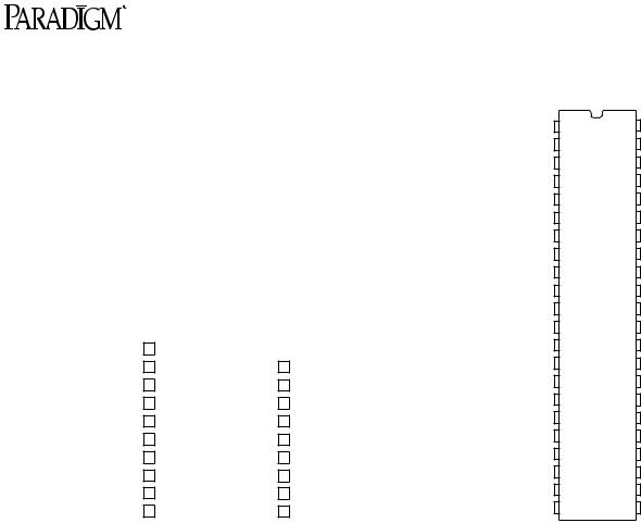
Pin Configuration
|
|
|
|
|
|
TSOP |
|
|
|
|
|
|
|
|
|
|
|
SOJ |
|
|
|
|
A4 |
|
|
|
|
|
|
|
|
|
|
A4 |
1 |
44 |
A5 |
||||
|
|
|
1 |
44 |
|
A5 |
|
|
||||||||||||
|
|
|
|
|||||||||||||||||
|
|
A3 |
|
2 |
43 |
|
A6 |
|
|
A3 |
2 |
43 |
A6 |
|||||||
|
|
|
|
|||||||||||||||||
|
|
A2 |
|
3 |
42 |
|
A7 |
|
|
A2 |
3 |
42 |
A7 |
|
||||||
|
|
|||||||||||||||||||
|
|
A1 |
|
|
41 |
|
|
|
|
|
|
|
A1 |
4 |
41 |
OE |
||||
|
|
|
4 |
|
OE |
|||||||||||||||
|
|
|
|
|
|
|
|
|
|
|
|
|
|
|
A0 |
|
40 |
|
|
|
|
|
A0 |
|
|
40 |
|
|
|
|
|
|
|
5 |
UB |
||||||
|
|
|
5 |
|
UB |
|||||||||||||||
|
|
|||||||||||||||||||
|
|
|
|
|
|
|
|
|
|
|
|
|
|
|
|
|
|
39 |
|
|
|
|
|
|
|
|
|
39 |
|
|
|
|
|
|
|
CE |
|
6 |
LB |
||
|
|
CE |
|
|
|
6 |
|
LB |
||||||||||||
I/O0 |
|
7 |
38 |
|
I/O15 |
I/O0 |
7 |
38 |
I/O15 |
|||||||||||
|
|
|||||||||||||||||||
|
|
|
||||||||||||||||||
I/O1 |
|
8 |
37 |
|
I/O14 |
I/O1 |
8 |
37 |
I/O14 |
|||||||||||
|
|
|||||||||||||||||||
I/O2 |
|
9 |
36 |
|
I/O13 |
I/O2 |
9 |
36 |
I/O13 |
|||||||||||
|
|
|||||||||||||||||||
I/O3 |
|
10 |
35 |
|
I/O12 |
I/O3 |
10 |
35 |
I/O12 |
|||||||||||
|
|
|||||||||||||||||||
Vcc |
|
11 |
34 |
|
Vss |
Vcc |
11 |
34 |
Vss |
|||||||||||
|
|
|||||||||||||||||||
Vss |
|
12 |
33 |
|
Vcc |
Vss |
12 |
33 |
Vcc |
|||||||||||
|
|
|||||||||||||||||||
I/O4 |
13 |
32 |
|
I/O11 |
I/O4 |
13 |
32 |
I/O11 |
||||||||||||
|
||||||||||||||||||||
I/O5 |
14 |
31 |
|
I/O10 |
I/O5 |
14 |
31 |
I/O10 |
||||||||||||
|
|
|
|
|
|
|
|
|
||||||||||||
I/O6 |
15 |
30 |
|
I/O9 |
I/O6 |
15 |
30 |
I/O9 |
||||||||||||
I/O7 |
16 |
29 |
|
I/O8 |
I/O7 |
16 |
29 |
I/O8 |
||||||||||||
|
|
|
|
|
|
|
|
|
|
|
|
|
|
WE |
17 |
28 |
NC |
|||
|
WE |
|
17 |
28 |
|
NC |
||||||||||||||
A16 |
18 |
27 |
|
A8 |
A16 |
18 |
27 |
A8 |
||||||||||||
A15 |
19 |
26 |
|
A9 |
A15 |
19 |
26 |
A9 |
||||||||||||
A14 |
20 |
25 |
|
A10 |
A14 |
20 |
25 |
A10 |
||||||||||||
A13 |
21 |
24 |
|
A11 |
A13 |
21 |
24 |
A11 |
||||||||||||
|
|
|
|
|
|
|
|
|
||||||||||||
A12 |
22 |
23 |
|
NC |
A12 |
22 |
23 |
NC |
||||||||||||
|
|
|
|
|
|
|
|
|
|
|
|
|
|
|
|
|
|
|
|
|
Pin Description
|
Name |
Description |
||||||
|
|
|
||||||
|
A16-A0 |
Address Inputs |
||||||
|
|
|
||||||
|
I/O15-I/O0 |
Data Inputs |
||||||
|
|
|
|
|
|
|
|
|
|
|
|
|
|
|
|
|
Chip Enable Input |
|
CE |
|||||||
|
|
|
|
|
|
|
|
|
|
|
|
|
|
|
|
|
Write Enable Input |
|
WE |
|||||||
|
|
|
|
|
|
|
||
|
|
|
|
|
|
|
Output Enable Input |
|
|
OE |
|||||||
|
|
|
|
|
|
|||
|
|
|
|
|
Data Byte Control Inputs |
|||
|
LB, |
UB |
||||||
|
|
|
||||||
|
NC |
No Connect |
||||||
|
|
|
||||||
|
Vss |
Ground |
||||||
|
VCC |
Power (+3.3V) |
||||||
Capacitance (TA = +25°C, f = 1.0 MHz)
|
Symbol |
|
Parameter |
Conditions |
Max. |
Unit |
|
|
|
|
|
|
|
|
|
|
CIN |
|
Input Capacitance |
VIN = VSS |
6 |
pF |
|
|
CI/O |
|
Output Capacitance |
VI/O = VSS |
8 |
pF |
|
NOTE: |
1. This parameter is determined by device characterization, but is not production tested. |
||||||
|
|
|
|
|
|
|
|
2 |
|
|
|
|
|
|
Rev. 1.3 - 4/13/98 |

|
PRELIMINARY |
PDM31548 |
Operating Mode
|
|
|
|
|
|
|
|
|
|
|
|
|
|
|
|
|
|
|
Mode |
|
CE |
|
|
OE |
|
WE |
|
|
LB |
|
|
UB |
|
I/O7-I/O0 |
I/O15-I/O8 |
Power |
|
|
|
|
|
|
|
|
|
|
|
|
|
|
|
|
|
|
|
|
Read |
|
L |
|
|
L |
|
|
H |
|
|
L |
|
|
L |
|
Output |
Output |
ICC |
|
|
|
|
|
|
|
|
|
|
|
H |
|
|
L |
|
High Impedance |
Output |
ICC |
|
|
|
|
|
|
|
|
|
|
|
L |
|
|
H |
|
Output |
High Impedance |
ICC |
Write |
|
L |
|
|
X |
|
|
L |
|
|
L |
|
|
L |
|
Input |
Input |
ICC |
|
|
|
|
|
|
|
|
|
|
|
H |
|
|
L |
|
High Impedance |
Input |
ICC |
|
|
|
|
|
|
|
|
|
|
|
L |
|
|
H |
|
Input |
High Impedance |
ICC |
Output Disable |
|
L |
|
|
H |
|
|
H |
|
|
X |
|
|
x |
|
High Impedance |
High Impedance |
ICC |
|
|
L |
|
|
X |
|
|
X |
|
|
H |
|
|
H |
|
High Impedance |
High Impedance |
ICC |
Standby |
|
H |
|
|
X |
|
|
X |
|
|
X |
|
|
X |
|
High Impedance |
High Impedance |
ISB |
NOTE: 1. H = VIH, L = VIL, X = DON’T CARE
Absolute Maximum Ratings (1)
Symbol |
Rating |
Com’l. |
Ind. |
Unit |
|
|
|
|
|
VTERM |
Terminal Voltage with Respect to VSS |
–0.5 to +4.6 |
–0.5 to +4.6 |
V |
TBIAS |
Temperature Under Bias |
–55 to +125 |
–65 to +135 |
°C |
TSTG |
Storage Temperature |
–55 to +125 |
–65 to +150 |
°C |
PT |
Power Dissipation |
1.5 |
1.5 |
W |
IOUT |
DC Output Current |
50 |
50 |
mA |
T |
Maximum Junction Temperature (2) |
125 |
145 |
°C |
j |
|
|
|
|
|
|
|
|
|
NOTE: 1. Stresses greater than those listed under ABSOLUTE MAXIMUM RATINGS may cause permanent damage to the device. This is a stress rating only and functional operation of the device at these or any other conditions above those indicated in the operational sections of this specification is not implied. Exposure to absolute maximum rating conditions for extended periods may affect reliability.
2.Appropriate thermal calculations should be performed in all cases and specifically for
those where the chosen package has a large thermal resistance (e.g., TSOP). The
calculation should be of the form: Tj = Ta + P * θja where Ta is the ambient temperature, P is average operating power and θja the thermal resistance of the package. For this product, use the following θja values:
SOJ: 59o C/W TSOP: 87o C/W
Recommended DC Operating Conditions
Symbol |
Description |
Min. |
Typ. |
Max. |
Unit |
|
|
|
|
|
|
VCC |
Supply Voltage |
3.0 |
3.3 |
3.6 |
V |
VSS |
Supply Voltage |
0 |
0 |
0 |
V |
Industrial |
Ambient Temperature |
–40 |
25 |
85 |
°C |
|
|
|
|
|
|
Commercial |
Ambient Temperature |
0 |
25 |
70 |
°C |
|
|
|
|
|
|
1
2
3
4
5
6
7
8
9
10
11
12
Rev. 1.3 - 4/13/98 |
3 |
 Loading...