


PARADIGM PDM31256SA12SOATY, PDM31256SA12SOI, PDM31256SA12SOITR, PDM31256SA12SOITY, PDM31256SA12SOTR Datasheet
...
PDM31256
Features
High-speed access times
Com’l: 10, 12, 15 and 20ns
Ind’l: 12, 15 and 20ns
Low power operation (typical)
-PDM31256SA Active: 200 mW Standby: 15mW
Single +3.3V (±0.3V) power supply
TTL-compatible inputs and outputs
Packages
Plastic SOJ (300 mil) - SO
Plastic TSOP (I) - T
3.3V 256K Static RAM
32K x 8-Bit
Description
The PDM31256 is a high-performance CMOS static RAM organized as 32,768 x 8 bits. Writing to this device is accomplished when the write enable (WE) and the chip enable (CE) inputs are both LOW. Reading is accomplished when WE remains HIGH and CE and OE are both LOW.
The PDM31256 operates from a single +3.3V power supply and all the inputs and outputs are fully TTLcompatible.
The PDM31256 is available in a 28-pin 300-mil plastic SOJ and a 28-pin plastic TSOP (I).
1
2
3
4
5
6
Functional Block Diagram
|
A 0 |
Decoder |
|
Memory |
|
|
|
|
• |
• |
|
|
|||
|
• |
|
• |
|
|
|
|
Addresses |
• |
|
• |
Matrix |
|
|
|
|
• |
|
• |
|
|
|
|
|
• |
|
• |
|
|
|
|
|
A14 |
|
• |
|
|
|
|
I/O0 |
|
|
|
• • |
• |
• |
• |
|
Input |
|
Column I/O |
|
|
||
|
|
|
|
|
|||
• |
|
Data |
|
|
|
|
|
• |
|
Control |
|
|
|
|
|
|
|
|
|
|
|
|
|
I/O7 |
|
|
|
|
• |
|
|
|
|
|
|
|
|
|
|
|
|
|
|
|
• |
|
|
CE |
|
|
|
|
• |
|
|
|
|
|
|
|
|
|
|
Control |
|
|
|
|
|
|
|
WE |
|
|
|
|
|
|
|
OE |
|
|
|
|
|
|
|
7
8
9
10
11
12
Rev. 3.3 - 4/29/98 |
1 |
PDM31256
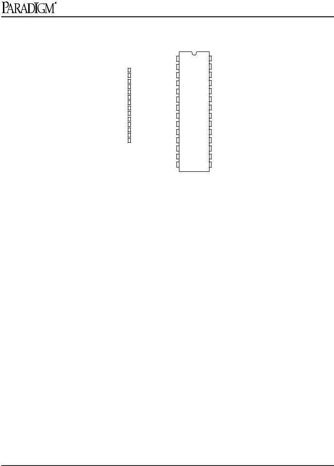
Pin Configurations
SOJ
Pin Description
|
|
|
|
|
TSOP |
|
|
A14 |
1 |
28 |
Vcc |
|
|
|
|
|
||
|
|
|
|
|
|
|
|
Name |
Description |
|||||||||
|
|
|
|
|
|
|
|
|
|
|
|
|
|
|||||
|
|
|
|
|
|
|
A10 |
A12 |
2 |
27 |
WE |
|||||||
|
|
|
|
|
|
|
|
|
|
|
|
|||||||
|
|
|
|
|
|
|
|
|
|
|
|
|||||||
|
OE |
|
22 |
21 |
|
|
|
A13 |
A14-A0 |
Address Inputs |
||||||||
A11 |
|
23 |
20 |
CE |
A7 |
3 |
26 |
|||||||||||
|
||||||||||||||||||
|
A9 |
|
24 |
19 |
I/O7 |
A6 |
4 |
25 |
|
A8 |
|
|
|
|
|
|||
|
A8 |
|
25 |
18 |
I/O6 |
|
I/O7-I/O0 |
Data Inputs/Outputs |
||||||||||
|
||||||||||||||||||
A13 |
|
26 |
17 |
I/O5 |
A5 |
5 |
24 |
|
A9 |
|
|
|
|
|
||||
WE |
|
27 |
16 |
I/O4 |
A4 |
6 |
23 |
A11 |
OE |
Output Enable Input |
||||||||
Vcc |
|
28 |
15 |
I/O3 |
|
|
|
|
|
|||||||||
A14 |
|
1 |
14 |
Vss |
A3 |
7 |
22 |
|
OE |
|
|
WE |
Write Enable Input |
|||||
|
|
|||||||||||||||||
A12 |
|
2 |
13 |
I/O2 |
|
|
|
|
|
|
|
|
|
|
|
|||
|
A7 |
|
3 |
12 |
I/O1 |
A2 |
8 |
21 |
A10 |
|
CE |
Chip Enable Input |
||||||
|
|
|||||||||||||||||
|
A6 |
|
4 |
11 |
I/O0 |
A1 |
9 |
20 |
|
CE |
|
|
|
|
|
|
||
|
|
|
|
|
VCC |
Power (+3.3V) |
||||||||||||
|
A5 |
|
5 |
10 |
A0 |
A0 |
10 |
19 |
I/O7 |
|
||||||||
|
||||||||||||||||||
|
A4 |
|
6 |
9 |
A1 |
|
VSS |
Ground |
||||||||||
|
|
|
|
18 |
|
|
|
|
||||||||||
|
A3 |
|
7 |
8 |
A2 |
I/O0 |
11 |
I/O6 |
|
|||||||||
|
|
|||||||||||||||||
|
|
|
|
|
|
|
|
I/O1 |
12 |
17 |
I/O5 |
|
|
|
|
|
||
|
|
|
|
|
|
|
|
I/O2 |
13 |
16 |
I/O4 |
|
|
|
|
|
||
|
|
|
|
|
|
|
|
Vss |
14 |
15 |
I/O3 |
|
|
|
|
|
||
Truth Table
|
|
|
|
|
|
|
|
|
|
|
|
OE |
|
WE |
|
|
CE |
|
I/O |
MODE |
|
|
|
|
|
|
|
|
|
|
|
|
|
X |
|
|
X |
|
|
H |
|
Hi-Z |
Standby |
|
|
|
|
|
|
|
|
|
|
|
|
L |
|
|
H |
|
|
L |
|
DOUT |
Read |
|
X |
|
|
L |
|
|
L |
|
DIN |
Write |
|
H |
|
|
H |
|
|
L |
|
Hi-Z |
Output Disable |
|
|
|
|
|
|
|
|
|
|
|
NOTE: 1. H = VIH, L = VIL, X = DON’T CARE
Absolute Maximum Ratings (1)
Symbol |
Rating |
Com’l. |
Ind. |
Unit |
|
|
|
|
|
VTERM |
Terminal Voltage with Respect to Vss |
–0.5 to +4.6 |
–0.5 to +4.6 |
V |
TBIAS |
Temperature Under Bias |
–55 to +125 |
–65 to +135 |
°C |
TSTG |
Storage Temperature |
–55 to +125 |
–65 to +150 |
°C |
PT |
Power Dissipation |
1.0 |
1.0 |
W |
IOUT |
DC Output Current |
50 |
50 |
mA |
T |
Maximum Junction Temperature (2) |
125 |
145 |
°C |
j |
|
|
|
|
|
|
|
|
|
NOTE: 1. Stresses greater than those listed under ABSOLUTE MAXIMUM RATINGS may cause permanent damage to the device. This is a stress rating only and functional operation of the device at these or any other conditions above those indicated in the operational sections of this specification is not implied. Exposure to absolute maximum rating conditions for extended periods may affect reliability.
2.Appropriate thermal calculations should be performed in all cases and specifically for
those where the chosen package has a large thermal resistance (e.g., TSOP). The
calculation should be of the form: Tj = Ta + P * θja where Ta is the ambient temperature, P is average operating power and θja the thermal resistance of the package. For this product, use the following θja values:
SOJ: 78 oC/W TSOP: 112 oC/W
2 |
Rev. 3.3 - 4/29/98 |

PDM31256
Recommended DC Operating Conditions
Symbol |
Parameter |
Min. |
Typ. |
Max. |
Unit |
|
|
|
|
|
|
VCC |
Supply Voltage |
3.0 |
3.3 |
3.6 |
V |
VSS |
Supply Voltage |
0 |
0 |
0 |
V |
Commercial |
Ambient Temperature |
0 |
25 |
70 |
°C |
|
|
|
|
|
|
Industrial |
Ambient Temperature |
–40 |
25 |
85 |
°C |
|
|
|
|
|
|
DC Electrical Characteristics (VCC = 3.3V ± 0.3V)
Symbol |
Parameter |
Test Conditions |
Min. |
Max. |
Unit |
||
|
|
|
|
|
|
||
ILI |
Input Leakage Current |
VCC = MAX., VIN |
–5 |
5 |
A |
||
|
|
|
= Vss to VCC |
|
|
|
|
ILO |
Output Leakage Current |
VCC= MAX., |
–5 |
5 |
A |
||
|
|
|
CE |
= VIH, VOUT = |
|
|
|
|
|
|
Vss to VCC |
|
|
|
|
VIL |
Input Low Voltage |
|
|
|
–0.3(1) |
0.8 |
V |
VIH |
Input High Voltage |
|
|
|
2.2 |
Vcc+0.3 |
V |
VOL |
Output Low Voltage |
IOL= 8 mA |
— |
0.4 |
V |
||
|
|
|
VCC = Min. |
|
|
|
|
VOH |
Output High Voltage |
IOH = –4 mA, |
2.4 |
— |
V |
||
|
|
|
VCC = Min. |
|
|
|
|
NOTE:1.VIL(min) = –3.0V for pulse width less than 20 ns.
1
2
3
4
5
6
7
Power Supply Characteristics
|
|
|
|
|
|
-10 |
-12 |
|
-15 |
|
-17 |
|
-20 |
|
|
||||
Symbol |
|
Parameter |
Com’l. |
Com’l |
Ind. |
Com’l |
Ind. |
Com’l |
Ind. |
Com’l |
|
Ind. |
Unit |
||||||
ICC |
|
Operating Current |
140 |
130 |
|
130 |
120 |
|
120 |
120 |
|
120 |
110 |
|
110 |
mA |
|||
|
|
CE |
|
= VIL |
|
|
|
|
|
|
|
|
|
|
|
|
|
|
|
|
|
f = fMAX = 1/tRC |
|
|
|
|
|
|
|
|
|
|
|
|
|
|
|||
|
|
VCC = Max. |
|
|
|
|
|
|
|
|
|
|
|
|
|
|
|||
|
|
IOUT = 0 mA |
|
|
|
|
|
|
|
|
|
|
|
|
|
|
|||
ISB |
|
Standby Current |
45 |
40 |
|
35 |
35 |
|
35 |
35 |
|
35 |
30 |
|
30 |
mA |
|||
|
|
CE |
|
= VIH |
|
|
|
|
|
|
|
|
|
|
|
|
|
|
|
|
|
f = fMAX = 1/tRC |
|
|
|
|
|
|
|
|
|
|
|
|
|
|
|||
|
|
VCC = Max. |
|
|
|
|
|
|
|
|
|
|
|
|
|
|
|||
ISB1 |
|
Full Standby Current |
10 |
10 |
|
15 |
10 |
|
15 |
10 |
|
15 |
10 |
|
15 |
mA |
|||
|
|
|
CE |
≥ VCC – 0.2V |
|
|
|
|
|
|
|
|
|
|
|
|
|
|
|
|
|
f = 0 |
|
|
|
|
|
|
|
|
|
|
|
|
|
|
|||
|
|
VCC = Max., |
|
|
|
|
|
|
|
|
|
|
|
|
|
|
|||
|
|
VIN ≥ VCC – 0.2V or ≤ 0.2V |
|
|
|
|
|
|
|
|
|
|
|
|
|
|
|||
NOTES: All values are maximum guaranteed values.
8
9
10
11
12
Rev. 3.3 - 4/29/98 |
3 |
 Loading...