

Panasonic TX-L32S20E Schematic

ORDER No. PCZ1004037CE
REVISION 3
Service Manual
Colour LCD Television
TX-L32S20E
TX-L32S20L
TX-LF32S20
TX-L32S20ES
TX-L37S20E
TX-L37S20L
TX-LF37S20
TX-L37S20ES
GLP25 Chassis
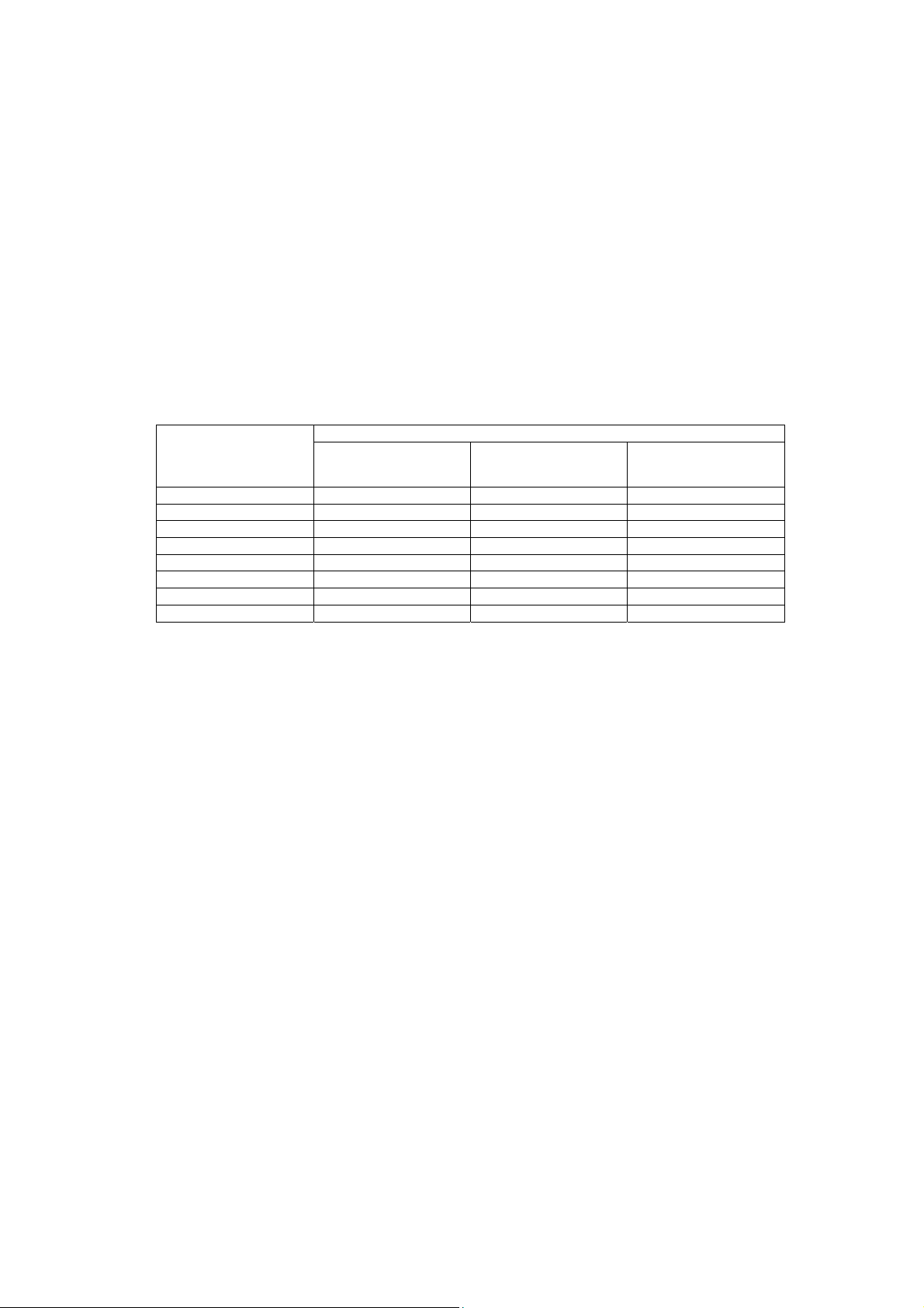
Specifications
(Information in brackets [ ] refers to model 32”)
Power Source: 220-240V AC, 50Hz
Rated Power Consumption: 145W [103W]
Stand-by Power Consumption: 0.25W (Without monitor out recording)
13W (With monitor out recording)
Aerial Impedance: 75Ω unbalanced, Coaxial Type
Receiving System:
PAL-I/H, B/G, D/K
SECAM B/G, D/K, L/L’
PAL-525/60 (AV only)
DVB-T (Digital Terrestrial Services (MPEG2 and MPEG4-AVC(H.264))
DVB-C (Digital cable services (MPEG2 and MPEG4-AVC(H.264))
M.NTSC (AV only)
NTSC (AV only)
Receiving Channels:
VHF E2-E12 VHF H1-H2 (ITALY)
VHF A-H (ITALY) VHF R1-R2
VHF R3-R5 VHF R6-R12
UHF E21-E69 CATV (S01-S05)
CATV S1-S10 (M1-M10) CATV S11-S20 (U1-U10)
CATV S21-S41 (Hyperband) VHF A-J (IRELAND)
Operating Conditions: Temperature: 0°C ÷ 35°C
Humidity: 20% ÷ 80% RH (non condensing)
PC signals: VGA, SVGA, XGA, SXGA(compressed)
Horizontal scanning frequency 31 – 69 kHz
Vertical scanning frequency 59 – 86 Hz
© Panasonic Corporation 2010.
Unauthorized copying
distribution is a violation of law.
and

Intermediate Frequency:
Video/Audio
Video 38,9MHz, 33,9MHz
Audio 33,4MHz (B/G), 33,16MHz (A2)
33,05MHz (NICAM B/G, D/K, L’)
32,4MHz (D/K), 32,66MHz (CZ STEREO)
40,4MHz (L’), 39,75MHz (L’ NICAM)
32,90 I, 32.35MHz (NICAM)
Colour 34,47MHz (PAL)
34,5MHz, 34,65MHz (SECAM)
38,3MHz, 38,15MHz (SECAM L’)
Terminals:
AV1 IN Video (21 pin) 1V p-p 75Ω
Audio (21 pin) 500mV rms 10kΩ
RGB (21 pin) 0.7V p-p 75Ω
S-video IN (21-pin) Y: 1V p-p 75Ω
C:0.3V p-p 75Ω
AV1 OUT Video (21 pin) 1V p-p 75Ω
Audio (21 pin) 500mV rms 1kΩ
AV2 IN Video (21 pin) 1.0V p-p 75Ω
Audio (21 pin) 500mV rms 1kΩ
RGB (21 pin) 0.7V p-p 75Ω
S-video IN (21-pin) Y: 1.0V p-p 75Ω
C:0.3V p-p 75Ω
AV2 OUT Video (21 pin) 1V p-p 75Ω
Audio (21 pin) 500mV rms 1kΩ
AV3 Video RCA PIN Type x 1 Y:1V p-p 75Ω
AUDIO IN Audio RCA PIN Type x 2 500mV rms 1kΩ
COMPONENT Video RCA PIN Type x 3 Y:1V p-p 75Ω (including synchronization)
Pb, Pr: ±0,35V p-p 75Ω
AUDIO IN Audio RCA PIN Type x 2 500mV rms 1kΩ
AUDIO OUT Audio (RCAx2) 500mV rms 1kΩ (high Impedance)
HDMI1/2/3 Type A Connector
HDMI1/3 :HDMI (Version 1.3a with Deep Colour)
HDMI 2 :HDMI (Version 1.4 with Audio Return Channel) and
HDMI (Version 1.3a with Deep Colour)
PC HIGH-DENSITY D-SUB 15PIN R,G,B: 700mV p-p 75Ω
HD,VD/TTL Level 2-5V p-p (high impedance)
CARD SLOT SD CARD slot ×1
Common Interface slot ×1 (Complies with CI+)
DIGITAL AUDIO OUT PCM / Dolby Digital / DTS , Fiber optic
LCD screen: L5EDD9T00027 [L5EDD8T00017]
1920 x 1080 XGA, 16:9
Visible Diagonal 940mm [800mm]
Audio Output: 20W (2x10W), 10% THD
Headphones: 3.5mm (M3), 8Ω Impedance
Accessories supplied : Remote Control 2 x R6 (UM3) Batteries
Dimensions:
Height: Width: Depth:
Including TV stand 621mm 915mm 287mm
[551mm] [798mm] [217mm]
TV set only 577mm 915mm 87mm
[511mm] [798mm] [83mm]
Net weight:
Including TV stand 15.5kg [11.5kg]
TV set only 13.0kg [9.5kg]
Specifications are subject to change without notice. Weights and dimensions shown are approximate.
Warning
This service information is designed for experienced repair technicians only and is not designed for use by the general public. It does not
contain warnings or cautions to advise non-technical individuals of potencial dangers in attempting to service a product. Products
powered by electricity should be serviced or repaired only by experienced professional technicians. Any attempt to service or repair the
product or products deal within this service information by anyone else could result in serious injury or death.
2

CONTENTS
SAFETY PRECAUTIONS..........................................................................4
GENERAL GUIDE LINES..................................................................... 4
TOUCH – CURRENT CHECK.............................................................. 4
PREVENTION OF ELECTROSTATIC DISCHARGE (ESD)
TO ELECTROSTATICALLY SENSITIVE (ES) DEVICES..........................5
ABOUT LEAD FREE SOLDER (PBF)........................................................ 6
SUGGESTED PB FREE SOLDER....................................................... 6
APPLICABLE SIGNALS............................................................................. 7
SERVICE HINTS ....................................................................................... 8
CHASSIS BOARD LAYOUT......................................................................9
LOCATION OF LEAD WIRING…………………………………………….9
TECHNICAL DESCRIPTION.....................................................................10
SETTING INSPECTION........................................................................... 11
SELF-CHECK .......................................................................................... 12
POWER LED BLINKING TIMING CHART...............................................14
SERVICE MODE FUNCTION.................................................................. 15
SERVICE ................................................................................................ 16
SERVICE TOOL MODE........................................................................... 17
HOTEL MODE ......................................................................................... 18
DATA COPY BY SD CARD ..................................................................... 19
DATA COPY FROM TV SET TO SD CARD............................................20
DATA COPY FROM TV SET TO TV SET................................................ 21
OPTION DESCRIPTION.......................................................................... 22
ADJUSTMENT METHOD ........................................................................ 23
WIRING DIAGRAM.................................................................................. 24
BLOCK DIAGRAMS................................................................................. 25
PARTS LOCATION.................................................................................. 26
REPLACEMENT PARTS LIST................................................................. 28
SCHEMATIC DIAGRAMS........................................................................ 42
A-BOARD (1 OF 21) SCHEMATIC DIAGRAM................................... 43
V-BOARD SCHEMATIC DIAGRAM ................................................... 62
CONDUCTOR VIEWS.............................................................................63
3
Safety Precautions
Ω
Ω
General Guide Lines
1. When servicing, observe the original lead dress. If a short circuit is found, replace all parts which have been overhe ated
or damaged by the short circuit.
2. After servicing, see to it that all the protective devices such as insulation barriers, insulation papers shields are properly
installed.
3. After servicing, make the following touch current checks to prevent the customer from being exposed to shock hazards.
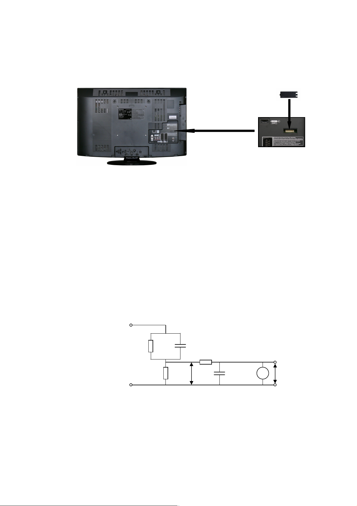
4. Always ensure panel TKP0E16001 is correctly replaced before returning to customer (see Fig.1).
Touch-Current Check
1. Plug the AC cord directly into the AC outlet. Do not use an isolation transformer for this check.
2. Connect a measuring network for touch currents between each exposed metallic part on the set and a good earth
ground such as a water pipe, as shown in Fig. 2.
3. Use Leakage Current Tester (Simpson 228 or equivalent) to measure the potential acr oss the measuring network.
4. Check each exposed metallic part, and measure the voltage at each point.
5. Reserve the AC plug in the AC outlet and repeat each of the above measure.
6. The potential at any point (TOUCH CURRENT) expressed as voltage U1 and U2, does not exceed the following values:
For a. c.: U1 = 35 V (peak) and U2 = 0.35 V (peak);
For d. c.: U1 = 1.0 V,
Note:
The limit value of U2 = 0.35 V (peak) for a. c. and U1 = 1.0 V for d. c. correspond to the values 0.7 mA (peak) a. c. and
2.0 mA d. c.
The limit value U1 = 35 V (peak) for a. c. correspond to the value 70 mA (peak) a. c. for frequencies greater than 100
kHz.
7. In case a measurement is out of the limits specified, there is a possibility of a shock hazard, and the equipment shoul d
be repaired and rechecked before it is returned to the customer.
COLD
WATER PIPE
(EARTH GROUND)
TO
APPLIANCES
EXPOSED
METAL PARTS
Resistance values in ohms (Ω)
V: Voltmetr or oscilloscope
(r.m.s. or peak reading)
NOTE – Appropriate measures should be taken to obtain the correct value in case of non-sinusoidal waveforms
Fig. 1
Measuring network for TOUCH CURRENTS
C
R
=1500Ω
S
R0=500Ω
Input resistance: ≥ 1M
Input capacitance: ≤ 200pF
Frequency range: 15Hz to 1MHz and d.c.respectively
Fig. 2
=0.22μF
S
U
10k
1
0.022μF
V
U2 (V)
4

Prevention of Electrostatic Discharge (ESD) to Electrostatically
Sensitive (ES) Devices
Some semiconductor (solid state) devices can be damaged easily by static electricity. Such components commonly are
called Electrostatically Sensitive (ES) Devices. Examples of typical ES devices are integrated circuits and some field-effect
transistors and semiconductor "chip" components. The following techniques should be used to help reduce the incidence of
component damage caused by electrostatic discharge (ESD).
1. Immediately before handling any semiconductor component or semiconductor-equipped assembly, drain off any ESD on
your body by touching a known earth ground. Alternatively, obtain and wear a commercially available discharging ESD
wrist strap, which should be removed for potential shock reasons prior to applying power to the unit under test.
2. After removing an electrical assembly equipped with ES devices, place the assembly on a conductive surface such as
aluminum foil, to prevent electrostatic charge build up or exposure of the assembly.
3. Use only a grounded-tip soldering iron to solder or unsolder ES devices.
4. Use only an anti-static solder removal device. Some solder removal devices not classified as "anti-static (ESD
protected)" can generate electrical charge sufficient to damage ES devices.
5. Do not use freon-propelled chemicals. These can generate electrical charges sufficient to damage ES devices.
6. Do not remove a replacement ES device from its protective package until immediately before you are ready to install it.
(Most replacement ES devices are packaged with leads electrically shorted together by cond uctive foam, aluminum foil
or comparable conductive material).
7. Immediately before removing the protective material from the leads of a replacement ES device, touch the protective
material to the chassis or circuit assembly into which the device will be installed.
Caution
Be sure no power is applied to the chassis or circuit, and observe all other safety precautions.
8. Minimize bodily motions when handling unpackaged replacement ES devices. (Otherwise harmless motion such as th e
brushing together of your clothes fabric or the lifting of your foot from a carpeted floor can generate static electricity
(ESD) sufficient to damage an ES device).
There are special components used in this equipment which are important for safety.
These parts are marked by in schematic diagrams, exploded views and replacement parts list. It is essent ial that
these critical parts should be replaced with manufacturer’s specified parts to prevent shock, fire, or other hazards. Do
not modify the original design without permission of manufacturer.
IMPORTANT SAFETY NOTICE
5

About lead free solder (PbF)
Note: Lead is listed as (Pb) in the periodic table of elements.
In the information below, Pb will refer to Lead solder, and PbF will refer to Lead Free Solder.
The Lead Free Solder used in our manufacturing process and discussed below is (Sn+Ag+Cu).
That is Tin (Sn), Silver (Ag) and Copper (Cu) although other types are available.
This model uses Pb Free solder in it’s manufacture due to environmental conservation issues. For service and repair work,
we’d suggest the use of Pb free solder as well, although Pb solder may be used.
PCBs manufactured using lead free solder will have the PbF within a leaf Symbol
stamped on the back of PCB.
Caution
• Pb free solder has a higher melting point than standard solder. Typically the melting point is 50 ~ 70 °F (30~40°C)
higher. Please use a high temperature soldering iron and set it to 700 ± 20 °F (370 ± 10 °C).
• Pb free solder will tend to splash when heated too high (a bout 1100 °F or 600 °C).
If you must use Pb solder, please completely remove all of the Pb free solder on the pins or solder area before
applying Pb solder. If this is not practical, be sure to heat the Pb free solder until it melts, before applying Pb solder.
• After applying PbF solder to double layered boards, please check the component side for excess solder which may
flow onto the opposite side. (see Fig.3)
Suggested Pb free solder
There are several kinds of Pb free solder available for purchase. This product uses Sn+Ag+Cu (tin, silver, copper) solder.
However, Sn+Cu (tin, copper), Sn+Zn+Bi (tin, zinc, bismuth) solder can also be used. (see Fig.4)
Fig.3
Fig.4
6
Applicable Signals
Component (Y, Pb, Pr), HDMI
525 (480) / 60i * *
525 (480) / 60p * *
625 (576) / 50i * *
625 (576) / 50p * *
750 (720) / 60p * *
750 (720) / 50p * *
1,125 (1,080) / 60i * *
1,125 (1,080) / 50i * *
1,125 (1,080) / 60p *
1,125 (1,080) / 50p *
1,125 (1,080) / 24p *
Applicable input signal for PC is basically compatible to VESA standard timing.
Signal name COMPONENT HDMI
PC (from D-sub 15P)
Signal name Horizontal frequency (kHz) Vertical frequency (Hz)
640 × 400 @70 Hz
640 × 480 @60 Hz
640 × 480 @75 Hz
800 × 600 @60 Hz
800 × 600 @75 Hz
800 × 600 @85 Hz
852 × 480 @60Hz
1,024 × 768 @60Hz
1,024 × 768 @70Hz
1,024 × 768 @75Hz
1,024 × 768 @85Hz
1,280 × 768 @60Hz
1,280 × 1,024 @60Hz
1,366 × 768 @60Hz
Macintosh 13“ (640 × 480)
Macintosh 16“ (832 × 624)
Macintosh 21“ (1,152 × 870)
PC (from HDMI terminal)
Applicable input signal for PC is basically compatible to HDMI standar d timing.
Signal name Horizontal frequency (kHz) Vertical frequency (Hz)
640 × 480 @60 Hz
750 (720) / 60p 45.00 60.00
1,125 (1,080) / 60p 67.50 60.00
Note:
• Signals other than above may not be displayed properly.
• The above signals are reformatted for optimal viewing on your display.
• PC signal is magnified or compressed for displa y, so that it may not be possible to show fine detail
with sufficient clarity.
31.47 70.07
31.47 59.94
37.50 75.00
37.88 60.32
46.88 75.00
53.67 85.06
31.44 59.89
48.36 60.00
56.48 70.07
60.02 75.03
68.68 85.00
47.70 60.00
63.98 60.02
48.39 60.04
35.00 66.67
49.73 74.55
68.68 75.06
31.47 60.00
7 7
Service Hints
How to remove the backcover
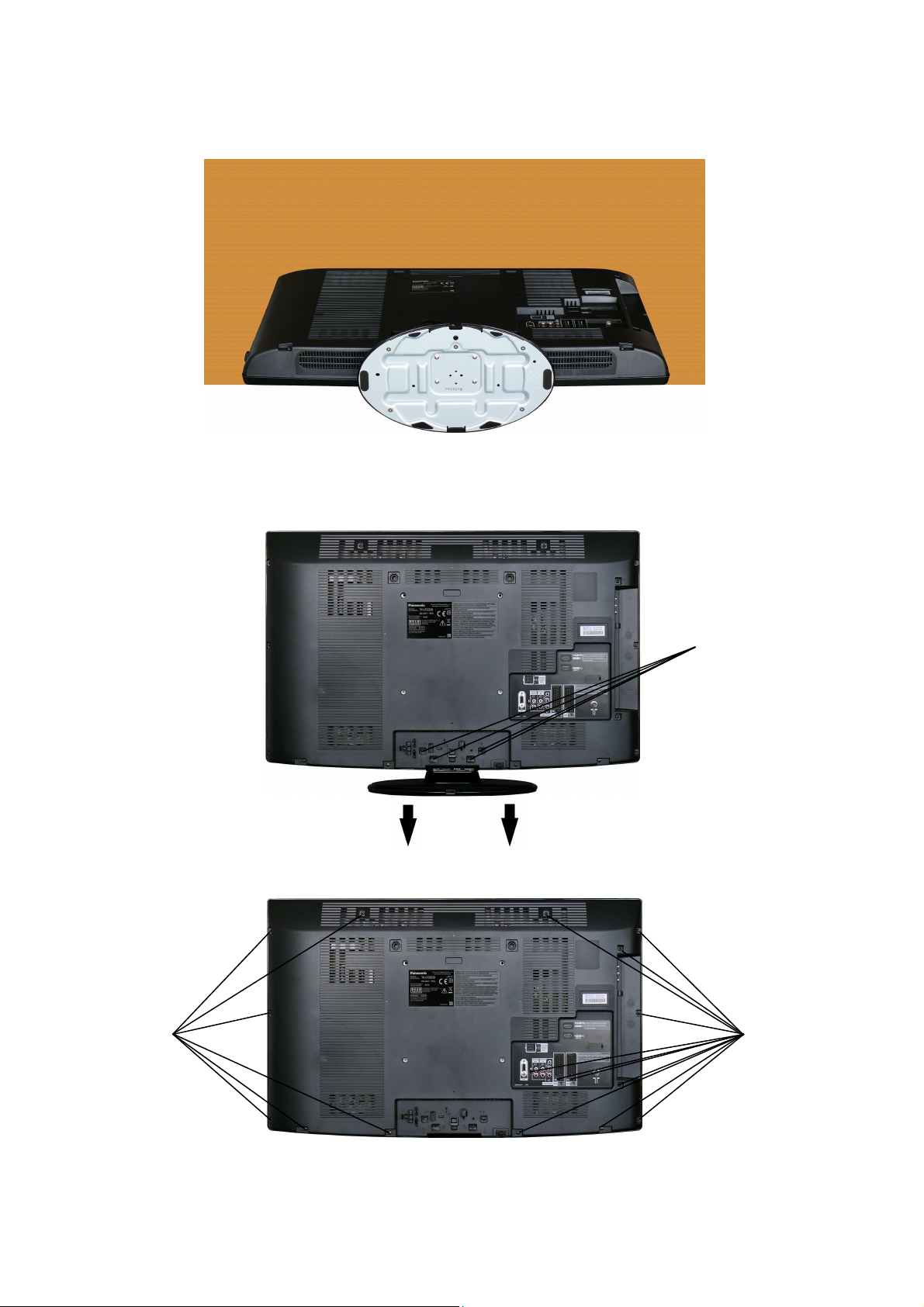
Lay the main unit face down. (see Fig.5)
How to remove the Pedestal assembly
Remove the 4 fixing screws and the pedestal assembly. (see Fig.6)
Remove the 17 fixing screws. (see Fig.7)
SCREWS
Fig.5
Fig.6
Fig.7
8
SCREWS
SCREWS
A
A
A
A
A
V
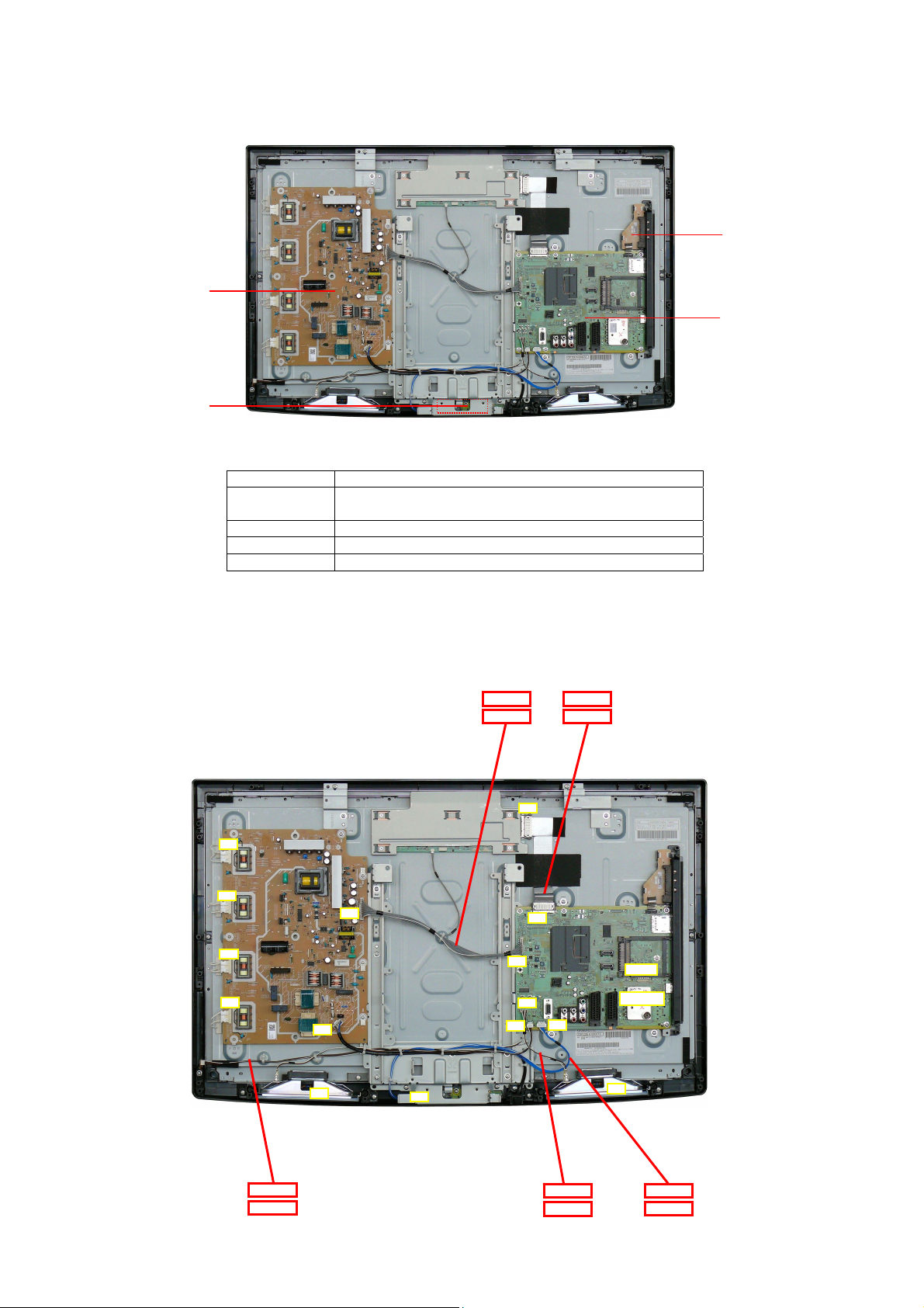
Chassis Board Layout
POWER UNIT
V-BOARD
Board Name Function
Tuner, AVSW,sLD,HDMI,CI Slot, Global
A-Board
Core, SD Slot, Speaker out
Power Unit Power Supply, Main Input
V-Board Remote Receiver, Cats, R/G LED
G-Unit Side AV Connector
Location of Lead Wiring
To find the Part Number of required wire in Replacement Parts List click on the wire name in red box.
( 37” )
( 32” )
( 37” )
A15-CN5 A09-P2
A15-CN5 A09-P2
( 32” )
G-UNIT
A-BOARD
CN5
P3
P4
P2
P5
P6
P1
15
09
12
10
02
CN0100
TU2901A
SP
10
SP
( 32” )
A02-S01
A02-S01
( 37” )
A12-SP
A12-SP
( 32” )
( 37” )
A10-V10
A10-V10
( 32” )
( 37” )
9
Technical Description
Specification of KEY for CI Plus, DTCP-IP and One-to-One
General information:
1. EEPROM (IC8950) for spare parts has the seed of KEY for each.
2. The final KEY data will be generated by sLD IC (IC8001) when SELF CHECK was done and are stored in both sLD IC
(IC800 1) and EEPROM (IC8950).
Three KEY are not generated for all models.
The necessary KEY are only generated and stored depend on the feature of models.
Replacement of ICs:
When sLD IC (IC8001) is replaced, EEPROM (IC8950) should be also replaced with new one the same time.
When EEPROM (IC8950) is replaced, sLD IC (IC8001) is not necessary to be replaced the same time.
After the replacement of IC, SELF CHECK should be done to generate the final KEY data.
How to SELF CHECK: While pressing [VOLUME ( - )] button on the main unit, press [MENU] button on the remote
control for more than 3 seconds.
TV will be forced to the factory shipment setting after this SELF CHECK.
Model and Keys:
Model No.
TX-L32S20E YES None None
TX-L32S20L YES None None
TX-LF32S20 None None None
TX-L32S20ES YES None None
TX-L37S20E YES None None
TX-L37S20L YES None None
TX-LF37S20 None None None
TX-L37S20ES YES None None
CI PLUS DTCP-IP
Keys
One-to_one
(for USB Rec.)
10

Setting Inspection
Voltage Confirmation
Confirm the following voltages:
A board
SUB1.8V TP5601 1.76V – 1.87V
SUB1.2V TP5600 1.18V – 1.29V
SUB3.3V TP5602 3.19V – 3.39V
SUB5V TP5200 4.9V – 5.1V
SUB9V TP5220 8.82V – 9.27V
STB5V TP5400 4.9V – 5.1V
TP No.
Voltage
11
Self Check
Self-check is used to automatically check the bus lines and hexadecimal code of the TV set. To enter Self-Check mode, keep
pressing the down (-/v) button on the TV set and press the STATUS button on the remote control. To exit Self Check,
switch off the TV set at the power button.
TX-L32S20E
TX-L32S20L
TX-LF32S20
TX-L32S20ES
TX-L37S20E
32FHD
TUN O.K.
STBY O.K.
MEM1 O.K.
MEM2 O.K.
ADAM O.K.
AVSW O.K.
OFDM O.K.
TEMP O.K.
VIF O.K.
ID O.K
32FHD
TUN O.K.
STBY O.K.
MEM1 O.K.
MEM2 O.K.
ADAM O.K.
AVSW O.K.
OFDM O.K.
TEMP O.K.
VIF O.K.
ID O.K
32FHD
TUN O.K.
STBY O.K.
MEM1 O.K.
MEM2 O.K.
ADAM O.K.
AVSW O.K.
OFDM O.K.
TEMP O.K.
VIF O.K.
ID O.K
32FHD
TUN O.K.
STBY O.K.
MEM1 O.K.
MEM2 O.K.
ADAM O.K.
AVSW O.K.
OFDM O.K.
TEMP O.K.
VIF O.K.
ID O.K
37FHD
TUN O.K.
STBY O.K.
MEM1 O.K.
MEM2 O.K.
ADAM O.K.
AVSW O.K.
OFDM O.K.
TEMP O.K.
VIF O.K.
ID O.K
Panasonic 2010LCD
Self Check Complete
PEAKS-SOFT 1.013
PEAKS-EEP 01.01.0012
LSI-PACKAGE 0.026
LSI-RELEASE 1.02
STBY-SOFT 1.00.00
STBY-EEP 1.01.3600
STBY-ROMCORR 0.00.00
Panasonic 2010LCD
Self Check Complete
PEAKS-SOFT 1.013
PEAKS-EEP 01.01.0028
LSI-PACKAGE 0.026
LSI-RELEASE 1.02
STBY-SOFT 1.00.00
STBY-EEP 1.01.3600
STBY-ROMCORR 0.00.00
Panasonic 2010LCD
Self Check Complete
PEAKS-SOFT 1.013
PEAKS-EEP 01.01.0014
LSI-PACKAGE 0.026
LSI-RELEASE 1.02
STBY-SOFT 1.00.00
STBY-EEP 1.01.3600
STBY-ROMCORR 0.00.00
Panasonic 2010LCD
Self Check Complete
PEAKS-SOFT 1.013
PEAKS-EEP 01.01.0012
LSI-PACKAGE 0.026
LSI-RELEASE 1.02
STBY-SOFT 1.00.00
STBY-EEP 1.01.3600
STBY-ROMCORR 0.00.00
Panasonic 2010LCD
Self Check Complete
PEAKS-SOFT 1.013
PEAKS-EEP 01.01.0015
LSI-PACKAGE 0.026
LSI-RELEASE 1.02
STBY-SOFT 1.00.00
STBY-EEP 1.01.3600
STBY-ROMCORR 0.00.00
SUM
MODEL ID
EDID
SUM
MODEL ID
EDID
SUM
MODEL ID
EDID
SUM
MODEL ID
EDID
SUM
MODEL ID
EDID
C405
07
030E6100
00000004
51 1909----
C405
07
030E6100
00000004
51 1909----
C411
07
03A96100
00000004
51 1909----
C405
07
030E6100
00000004
51 1909----
C31F
07
030E6100
00000010
51 1909----
12
TX-L37S20L
TX-LF37S20
TX-L37S20ES
37FHD
TUN O.K.
STBY O.K.
MEM1 O.K.
MEM2 O.K.
ADAM O.K.
AVSW O.K.
OFDM O.K.
TEMP O.K.
VIF O.K.
ID O.K
37FHD
TUN O.K.
STBY O.K.
MEM1 O.K.
MEM2 O.K.
ADAM O.K.
AVSW O.K.
OFDM O.K.
TEMP O.K.
VIF O.K.
ID O.K
37FHD
TUN O.K.
STBY O.K.
MEM1 O.K.
MEM2 O.K.
ADAM O.K.
AVSW O.K.
OFDM O.K.
TEMP O.K.
VIF O.K.
ID O.K
Panasonic 2010LCD
Self Check Complete
PEAKS-SOFT 1.013
PEAKS-EEP 01.01.0012
LSI-PACKAGE 0.026
LSI-RELEASE 1.02
STBY-SOFT 1.00.00
STBY-EEP 1.01.3600
STBY-ROMCORR 0.00.00
Panasonic 2010LCD
Self Check Complete
PEAKS-SOFT 1.013
PEAKS-EEP 01.01.0017
LSI-PACKAGE 0.026
LSI-RELEASE 1.02
STBY-SOFT 1.00.00
STBY-EEP 1.01.3600
STBY-ROMCORR 0.00.00
Panasonic 2010LCD
Self Check Complete
PEAKS-SOFT 1.013
PEAKS-EEP 01.01.0015
LSI-PACKAGE 0.026
LSI-RELEASE 1.02
STBY-SOFT 1.00.00
STBY-EEP 1.01.3600
STBY-ROMCORR 0.00.00
SUM
MODEL ID
EDID
SUM
MODEL ID
EDID
SUM
MODEL ID
EDID
C405
07
030E6100
00000010
51 1909----
CD66
07
03A96100
00000010
51 1909----
C31F
07
030E6100
00000010
51 1909----
Display Ref. No. Description P.C.B.
TUN TU2901A TUNER A-Board
STBY IC8001 sLD/STM A-Board
MEM1 IC1101 EEPROM (sLD/STM) A-Board
MEM2 IC8950 EEPROM (sLD) A-Board
ADAM IC8001 sLD A-Board
AVSW IC3000 AUDIO VIDEO SWITCH A-Board
OFDM IC8300 DEMODULATOR A-Board
TEMP IC9980 TEMP SENSOR A-Board
VIF TU2901A TUNER A-Board
If the CCU ports have been checked and found to be incorrect or not located then " - - " will appear in place of "O.K.".
13
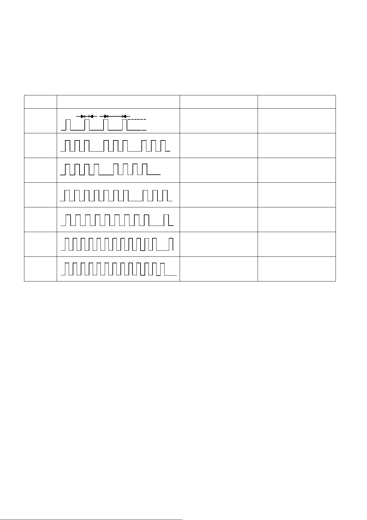
Power LED blinking timing chart
1. Subject
Information of LED Flashing timing chart.
2. Contents
When abnormality has occurred the unit, the protection circuit operates and reset to the stand by mode. At this time, the
defective block can be identified by number of blinking of the Power LED on the front panel of the unit.
Blinking
times
Once
1 BL_SOS A BOARD, P UNIT
3 SOS
4
7 SUB3.3V_SENSE_SOS A BOARD
Blinking timing Contents Check point
4 sec
Light
No Light
A BOARD
SUB12V_SENSE_SOS A BOARD, P UNIT
9 SOUND_SOS A BOARD, P UNIT
12
13 EMERGENCY SOS A BOARD
BE(sLD) SOS A BOARD
14

Service Mode Function
MPU controls the functions switching for each IICs through IIC bus in this chassis. The following setting and adjustment can be
adjusted by remote control in Service Menu
How to enter SERVICE
While pressing (-/v) button on TV unit, press on the remote
control for 3 times within 2 seconds.
Note:
To exit from Service mode, press the exit button on remote control.
0
15

SERVICE
A
A
A
A
A
A
SERVICE
ADJUST
WB-ADJ
OPTION
SRV-TOOL
Peaks SOFT 1.013 OPTION 1 0c
Peaks EEP 01.01.0012 OPTION 2 ee
LSI PACKAGE 0.026 OPTION 3 01
LSI DATA 1.00.01 OPTION 4 00
STBY SOFT 1.00.00 Model ID 07
STBY EEP 1.01.3600 03256100
STBY ROMCOR 0.00.00 00000010
R/E Cnt 000/000
INV Cnt 0000
1
ADJUST DYNAMIC
CONTRAST
YMAX
1,2:MAIN SELECT
3,4:SUB SELECT
9 :PICTURE MENU SELECT
YELLOW:AUTO ADJUST
VOL:ADJUST
OK :WRITE
1
WB-ADJ DYNAMIC
R-GAIN
BEFORE
METHOD
COLOR TEMP NORMAL
1,2:MAIN SELECT
3,4:SUB SELECT
7 :COLOR TEMP SELECT
9 :PICTURE MENU SELECT
0 :WB METHOD SELECT
VOL:ADJUST
OK :WRITE/WB DIFF ADJ
1
OPTION DYNAMIC
Boot
1,2:MAIN SELECT
3,4:SUB SELECT
9 :PICTURE MENU SELECT
VOL:ADJUST
1
SRV-TOOL DYNAMIC
000
FF
FF
02
ROM
00
2
ADJUST DYNAMIC
3
COLOR
1,2:MAIN SELECT
4
3,4:SUB SELECT
9 :PICTURE MENU SELECT
VOL:ADJUST
OK :WRITE
2
WB-ADJ DYNAMIC
G-GAIN
3
BEFORE
METHOD
COLOR TEMP NORMAL
1,2:MAIN SELECT
3,4:SUB SELECT
4
7 :COLOR TEMP SELECT
9 :PICTURE MENU SELECT
0 :WB METHOD SELECT
VOL:ADJUST
OK :WRITE/WB DIFF ADJ
2
OPTION DYNAMIC
STBY-SET
3
1,2:MAIN SELECT
4
3,4:SUB SELECT
9 :PICTURE MENU SELECT
OK :POWER OFF
2
31
E6
02
00
E6
DJUST DYNAMIC
3
TINT
1,2:MAIN SELECT
4
3,4:SUB SELECT
9 :PICTURE MENU SELECT
VOL:ADJUST
OK :WRITE
WB-ADJ DYNAMIC
B-GAIN
3
BEFORE
METHOD
COLOR TEMP NORMAL
1,2:MAIN SELECT
3,4:SUB SELECT
4
7 :COLOR TEMP SELECT
9 :PICTURE MENU SELECT
0 :WB METHOD SELECT
VOL:ADJUST
OK :WRITE/WB DIFF ADJ
OPTION DYNAMIC
Emergency
3
1,2:MAIN SELECT
4
3,4:SUB SELECT
9 :PICTURE MENU SELECT
VOL:ADJUST
Key Command
• Press the 3/4 button to change the adjustment values or function.
• Press the 1/2 button to step up/down through the functions and adjustments
• Press the numerical button VOLUME (+/-) to change option item.
• Press the OK button after each adjustment has been made to store the required values.
00
ON
CC
CC
02
ADJUST DYNAMIC
3
SUB-BRT
1,2:MAIN SELECT
4
3,4:SUB SELECT
9 :PICTURE MENU SELECT
VOL:ADJUST
OK :WRITE
WB-ADJ DYNAMIC
R-CENT
3
BEFORE
METHOD
COLOR TEMP NORMAL
1,2:MAIN SELECT
3,4:SUB SELECT
4
7 :COLOR TEMP SELECT
9 :PICTURE MENU SELECT
0 :WB METHOD SELECT
VOL:ADJUST
OK :WRITE/WB DIFF ADJ
OPTION DYNAMIC
Y/C Delay
3
1,2:MAIN SELECT
4
3,4:SUB SELECT
9 :PICTURE MENU SELECT
VOL:ADJUST
OK :WRITE
800
75
75
02
DJUST DYNAMIC
3
BACKLIGHT
1,2:MAIN SELECT
4
3,4:SUB SELECT
9 :PICTURE MENU SELECT
VOL:ADJUST
OK :WRITE
WB-ADJ DYNAMIC
G-CENT
3
BEFORE
METHOD
COLOR TEMP NORMAL
1,2:MAIN SELECT
3,4:SUB SELECT
7 :COLOR TEMP SELECT
9 :PICTURE MENU SELECT
0 :WB METHOD SELECT
VOL:ADJUST
OK :WRITE/WB DIFF ADJ
OPTION DYNAMIC
OPT 1
3
1,2:MAIN SELECT
4
3,4:SUB SELECT
5,6:BIT SELECT
9 :PICTURE MENU SELECT
VOL:ADJUST
OK :WRITE
554
80
80
02
00001100
DJUST DYNAMIC
H-POS
3
1,2:MAIN SELECT
4
3,4:SUB SELECT
9 :PICTURE MENU SELECT
VOL:ADJUST
OK :WRITE
WB-ADJ DYNAMIC
B-CENT
3
BEFORE
METHOD
COLOR TEMP NORMAL
1,2:MAIN SELECT
3,4:SUB SELECT
4 4
7 :COLOR TEMP SELECT
9 :PICTURE MENU SELECT
0 :WB METHOD SELECT
VOL:ADJUST
OK :WRITE/WB DIFF ADJ
OPTION DYNAMIC
OPT 2
3
1,2:MAIN SELECT
4
3,4:SUB SELECT
5,6:BIT SELECT
9 :PICTURE MENU SELECT
VOL:ADJUST
OK :WRITE
9F
02
11101110
9F
DJUST DYNAMIC
0
H-AMP
3
1,2:MAIN SELECT
4
3,4:SUB SELECT
9 :PICTURE MENU SELECT
VOL:ADJUST
OK :WRITE
OPTION DYNAMIC
OPT 3
3
1,2:MAIN SELECT
4
3,4:SUB SELECT
5,6:BIT SELECT
9 :PICTURE MENU SELECT
VOL:ADJUST
OK :WRITE
0
00000001
ADJUST DYNAMIC
V-POS
3
1,2:MAIN SELECT
4
3,4:SUB SELECT
9 :PICTURE MENU SELECT
VOL:ADJUST
OK :WRITE
OPTION DYNAMIC
OPT 4
3
1,2:MAIN SELECT
4
3,4:SUB SELECT
5,6:BIT SELECT
9 :PICTURE MENU SELECT
VOL:ADJUST
OK :WRITE
00000000
DJUST DYNAMIC
0
V-AMP
3
1,2:MAIN SELECT
4
3,4:SUB SELECT
9 :PICTURE MENU SELECT
VOL:ADJUST
OK :WRITE
4
DJUST DYNAMIC
VCOM
BEFORE
1,2:MAIN SELECT
3,4:SUB SELECT
5 :FLICKER PATTERN
9 :PICTURE MENU SELECT
VOL:ADJUST
OK :WRITE
OPTION DYNAMIC
EDID-CLK
3
HDMI
1,2:MAIN SELECT
4
3,4:SUB SELECT
7 :HDMI SELECT
9 :PICTURE MENU SELECT
VOL:ADJUST
OK :WRITE
3
17C
17C
MID
1
0
1,2:MAIN SELECT
9 :PICTURE MENU SELECT
OK :ENTER
16

Service Tool Mode
How to access
1. Select [SRV-TOOL] in Service Mode.
2. Press [OK] button on the remote control.
Display of TD2Microcode version
Display of Flash ROM maker code
Display of SOS History
SRV-TOOL
TD2Microcode:005a0910
Flash ROOM: AD – F1
PTCT:00.00.00.00.00 Time 00051:30 On/Off 0000042
Display of SOS History
SOS History (Number of LED blinking) indication.
From left side; Last SOS, before Last, three occurrence before, 2
This indication will be cleared by [Self/check indication and forced to factory shipment setting].
nd
occurrence after shipment, 1st occurrence after shipment.
Power ON Time, On/Off
Note: To display TIME/COUNT menu, highlight position, then press MUTE for 3sec.
Time: Cumulative power on time, indicated hour: minute by decimal.
On/Off: Number of On/Off switching by decimal.
Note: This indication will not be cleared by either of the self-checks or any other command.
Exit
Disconnect the AC cord from wall outlet or switch off the power with [Power] button on the main unit.
POWER ON TIME/COUNT
Press [MUTE] button (3sec)
17
Hotel Mode
1. Purpose
Restrict a function for hotels.
2. Access command to the Hotel mode setup menu.
In order to display the Hotel mode setup menu,
please enter the following command (within 2 second).
[TV] : Vol.[Down] + [REMOTE] : AV (3 times)
Then, the Hotel mode setup menu is displayed.
Hotel mode
Hotel mode
Initial INPUT
Initial POS
Off
Off
Off
Initial VOL Level
Maximum Vol Level
Button Lock
Remote Lock
Off
Off
Off
Off
Select
EXIT
Change
RETURN
3. To exit the Hotel mode setup menu.
Disconnect AC power cord from wall outlet.
4. Explain the Hotel mode setup menu.
ITEM Function
Hotel Mode Select hotel mode ON/OFF
Initial INPUT Select input signal modes.
Initial POS Select programme number.
Initial VOL Level Adjust the volume when each time power is
Maximum VOL
Level
Button Lock Select local key conditions.
Remote Lock Select remote control key conditions.
Set the input, when each time power is switched on.
Selection:
Off Analog /DVB-C/DVB-T/
AV1/AV1S/AV2/AV2S/AV3
Component/HDMI1/HDMI2/ HDMI3
*Off: give priority to the last memory. However, Euro
Model is compulsorily set to TV.
*AVnS/AVnC: only Euro model selectable
* PC:selectable with VGA option
Selection:
Off/0 to 99
*Off: give priority to the last memory
switched on.
Selection/Range:
Off/0 to 100
*Off: give priority to the last memory
Adjust maximum volume.
Range:
0 to 100
Selection:
Off/SETUP/MENU/ALL
*Off: altogether valid
*Setup: only F-key is invalid
(Tuning guide (menu) can not be selected.)
*MENU: only F-key is invalid
(only Volume/Mute can be selected.)
*All: altogether invalid.
Selected”
Off/SETUP/MENU
*Off: altogether valid
*Setup: only Setup menu is invalid
MENU: Picture/Sound/Setup menu are invalid
18
Data Copy by SD Card
Purpose
a) Board replacement (Copy the data when exchanging A-board):
W hen axchanging A-board, the data in original A-board can be copied to SD card and then copy to new A-board.
TV
A-board
(Before exchanging)
Copy to SD card
(After exchanging)
Copy back from SD card
SD
Following data can be copied.
User setting data
(inc. Hotel mode setting data)
Channel scan data
Adjustment and factory preset data
b) Hotel (Copy the data when installing a number of units in hotel or any facility):
W hen installing a number of units in hotel or any facility, the data in master TV can be copied to SD card and the copy
to other TVs.
Master TV
Copy to SD card
SD
Other TV
Copy from SD card
Other TV
Other TV
Following data can be copied.
User setting data
(inc. Hotel mode setting data)
Channel scan data
Preparation
Make pwd.file as startup file for (a) or (b) in an empty SD card.
1. Insert an empty SD card to your PC.
2. Right-click a blank area in a SD card window, point to New, and then click text document. A new file is created by
default (New Text Document.txt).
3. Right-click the new text document that you just created and select rename, and then change the name and extension
of the file to the following file name (a) or (b) and press ENTER.
File name:
(a) For Board replacement: boardreplace.pwd
(b) For Hotel: hotel.pwd
Note:
Please make only one file to prevent the operation error.
No any other file should be in SD card.
19
Data Copy from TV set to SD Card
1. Turn on the TV set.
2. Insert SD card with a startup file (pwd.file) to SD slot.
On-screen Display will be appeared according to the startu p file automatically.
3. Input a following password for (a) or (b) by using remote control.
(a) For Board replacement: 2770
(b) For Hotel: 4850
Data will be copied from TV set to SD card.
It takes around 2 to 6 minutes maximum for copying.
4. After the completion of copying to SD card, remove SD card from TV set.
5. Turn off the TV set.
Note:
Following new folder will be created in SD card for data from TV set.
(a) For Board replacement: user_setup
(b) For Hotel: hotel
Please do not remove the SD card
Data copy has been successful
Data Copy(Board replacement )
Input password
Data Copy(Board replacement )
Input password
Data Copy(Board replacement )
Copy TV to SD card
Please wait for a while
Data Copy(Board replacement )
Performing
Please remove SD card
Data copy
(Board replacement) or (Hotel)
-----
Input Password
2770 or 4850
-----
Performing
GETTING
Completion
FINISH
20
 Loading...