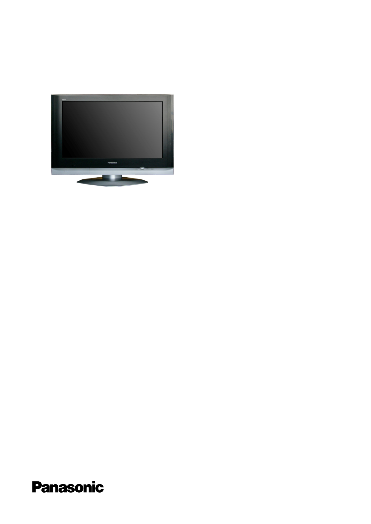
ORDER No. PCZ0608056CE
Service Manual
Colour LCD Television
TX-32LX600F
TX-32LX600P
TX-26LX600F
TX-26LX600P
LH50 Chassis
Specifications
(Informations in brackets [ ] refers to models 26´´)
Power Source: 220-240V AC, 50/60Hz
Power Consumption 136W TX-32LX600F
Stand-by Power Consumption: 0,4W
Aerial Impedance: 75Ω unbalanced, Coaxial Type
Receiving System: PAL-I, B/G, H, D/K,
Receiving Channels:
Operating Conditions: Temperature: 0°C ÷ 35°C
Scanning format: 480i(60Hz), 480p(60Hz), 576i(50Hz), 576p(50Hz), 720p(60Hz), 720p(50Hz), 1.080i(60Hz),
PC signals: VGA, SVGA, XGA
Intermediate Frequency:
Video/Audio
Video 38,9MHz, 33,9MHz
Audio 33,4MHz (B/G), 33,16MHz (A2)
Colour 34,47MHz (PAL)
Terminals:
AV1 IN Video (21 pin) 1V p-p 75Ω
169W TX-32LX600P
82W TX-26LX600F
118W TX-26LX600P
SECAM B/G, D/K, L/L’
PAL-525/60, M.NTSC, NTSC (AV only)
VHF E2-E12 VHF H1-H2 (ITALY)
VHF A-H (ITALY) VHF R1-R2
VHF R3-R5 VHF R6-R12
UHF E21-E69 CATV (S01-S05)
CATV S1-S10 (M1-M10) CATV S11-S20 (U1-U10)
CATV S21-S41 (Hyperband)
1.080i(50Hz)
SXGA(compressed)
Horizontal scanning frequency 31 – 69 kHz
Vertical scanning frequency 59 – 86 Hz
33,05MHz (NICAM B/G, D/K, L)
32,4MHz (D/K), 32,66MHz (CZ STEREO)
40,4MHz (L’), 39,75Mhz (L’NICAM),
34,5MHz, 34,65MHz (SECAM)
38,3MHz, 38,15MHz (SECAM L’)
Audio (21 pin) 500mV rms 10kΩ
RGB (21 pin) 0,7V p-p 75Ω

AV1 OUT Video (21 pin) 1V p-p 75Ω
AV2 IN Video (21 pin) 1V p-p 75Ω
AV2 OUT Video (21 pin) 1V p-p 75Ω
AV3 IN Video (21 pin) 1V p-p 75Ω
AV3 OUT Video (21 pin) 1V p-p 75Ω
AV4 IN S-Video IN (4-pin) Y: 1V p-p 75Ω
HDMI1, HDMI2 Type A Connector
COMPONENT YUV Video (RCAx3) Y:1V p-p 75Ω
AUDIO IN Audio (RCAx2) 500mV rms 10kΩ
AUDIO OUT Audio (RCAx2) 500mV rms 1kΩ
PC HIGH-DENSITY D_SUB 15PIN
CARD SLOT SD CARD slot x1
Audio (21 pin) 500mV rms 1kΩ
Audio (21 pin) 500mV rms 10kΩ
S-video IN (21-pin)Y: 1V p-p 75Ω
C:0,3V p-p 75Ω
Audio (21 pin) 500mV rms 1kΩ
Audio (21 pin) 500mV rms 10kΩ
RGB (21 pin) 0,7V p-p 75Ω
S-video IN (21-pin)Y: 1V p-p 75Ω
C:0,3V p-p 75Ω
Audio (21 pin) 500mV rms 1kΩ
C:0,3V p-p 75Ω
Audio (RCAx2) 500mV rms 10kΩ
Video (RCAx1) 1V p-p 75Ω
Pb, Pr: 0,7V p-p 75Ω
LCD screen: L5EDD8Q00025 [L5EDD6Q00019]
Audio Output: 20W (5W + 5W, 5W + 5W)
Headphones: 3,5mm, 8Ω Impedance
Accessories supplied : Remote Control 2 x R6 (UM3) Batteries
Dimensions:
Including TV stand 624mm 857mm 300mm
TV set only 563mm 857mm 141mm
Net weight: 22,5kg [19,5kg]
Specifications are subject to change without notice.
Weights and dimensions shown are approximate.
1366 x 768 XGA, 16:9
Visible Diagonal 800mm [660mm]
Height: Width: Depth:
[549mm] [724mm] [300mm]
[487mm] [724mm] [141mm]
Warning
This service information is designed for experienced repair technicians only and is not designed for use by the general public. It does not
contain warnings or cautions to advise non-technical individuals of potencial dangers in attempting to service a product. Products
powered by electricity should be serviced or repaired only by experienced professional technicians. Any attempt to service or repair the
product or products deal within this service information by anyone else could result in serious injury or death.
2

CONTENTS
SAFETY PRECAUTIONS ........................................... 4
GENERAL QUIDE LINES...................................... 4
TOUCH – CURRENT CHECK............................... 4
PREVENTION OF ELECTROSTATIC DISCHARGE
(ESD) TO ELECTROSTATICALLY SENSITIVE (ES)
DEVICES .................................................................... 5
ABOUT LEAD FREE SOLDER (PBF)......................... 6
SUGGESTED PB FREE SOLDER........................ 6
APPLICABLE SIGNALS.............................................. 7
SERVICE HINTS ........................................................ 8
CHASSIS BOARD LAYOUT ....................................... 9
SETTING INSPECTION.............................................. 9
SELF-CHECK ........................................................... 10
POWER LED BLINKING TIMING CHART ................ 11
SERVICE MODE FUNCTION ................................... 12
SERVICE 1 ............................................................... 13
SERVICE 2 ............................................................... 14
OPTION DESCRIPTION........................................... 15
ADJUSTMENT METHOD ......................................... 17
WIRING DIAGRAM................................................... 18
BLOCK DIAGRAMS.................................................. 19
PARTS LOCATION................................................... 22
REPLACEMENT PARTS LIST.................................. 24
SCHEMATIC DIAGRAMS ......................................... 49
AP-BOARD (1 OF 3) SCHEMATIC DIAGRAM.... 50
AP-BOARD (2 OF 3) SCHEMATIC DIAGRAM.... 51
AP-BOARD (3 OF 3) SCHEMATIC DIAGRAM.... 52
DG-BOARD (1 OF 8) SCHEMATIC DIAGRAM ... 53
DG-BOARD (2 OF 8) SCHEMATIC DIAGRAM ... 54
DG-BOARD (3 OF 8) SCHEMATIC DIAGRAM ... 55
DG-BOARD (4 OF 8) SCHEMATIC DIAGRAM ... 56
DG-BOARD (5 OF 8) SCHEMATIC DIAGRAM ... 57
DG-BOARD (6 OF 8) SCHEMATIC DIAGRAM ... 58
DG-BOARD (7 OF 8) SCHEMATIC DIAGRAM ... 59
DG-BOARD (8 OF 8) SCHEMATIC DIAGRAM ... 60
G-BOARD SCHEMATIC DIAGRAM .................... 61
GS-BOARD SCHEMATIC DIAGRAM.................. 62
H-BOARD (1 OF 4) SCHEMATIC DIAGRAM...... 63
H-BOARD (2 OF 4) SCHEMATIC DIAGRAM...... 64
H-BOARD (3 OF 4) SCHEMATIC DIAGRAM...... 65
H-BOARD (4 OF 4) SCHEMATIC DIAGRAM...... 66
V ,K-BOARD SCHEMATIC DIAGRAM ................ 67
CONDUCTOR VIEWS......................................... 68
3
Safety Precautions
A
Ω
Ω
Ω
Ω
General Guide Lines
1. When servicing, observe the original lead dress. If a short circuit is found, replace all parts which have been overheated
or damaged by the short circuit.
2. After servicing, see to it that all the protective devices such as insulation barriers, insulation papers shields are properly
installed.
3. After servicing, make the following touch current checks to prevent the customer from being exposed to shock hazards.
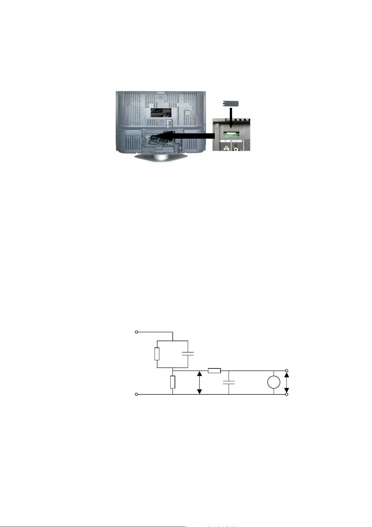
4. Always ensure panel TKKL5290 is correctly replaced before returning to customer (see Fig.1).
Fig. 1
Touch-Current Check
1. Plug the AC cord directly into the AC outlet. Do not use an isolation transformer for this check.
2. Connect a measuring network for touch currents between each exposed metallic part on the set and a good earth
ground such as a water pipe, as shown in Fig. 2.
3. Use Leakage Current Tester (Simpson 228 or equivalent) to measure the potential across the measuring network.
4. Check each exposed metallic part, and measure the voltage at each point.
5. Reserve the AC plug in the AC outlet and repeat each of the above measure.
6. The potential at any point (TOUCH CURRENT) expressed as voltage U1 and U2, does not exceed the following values:
For a. c.: U1 = 35 V (peak) and U2 = 0.35 V (peak);
For d. c.: U1 = 1.0 V,
Note:
The limit value of U2 = 0.35 V (peak) for a. c. and U1 = 1.0 V for d. c. correspond to the values 0.7 mA (peak) a. c. and
2.0 mA d. c.
The limit value U1 = 35 V (peak) for a. c. correspond to the value 70 mA (peak) a. c. for frequencies greater than 100
kHz.
7. In case a measurement is out of the limits specified, there is a possibility of a shock hazard, and the equipment should
be repaired and rechecked before it is returned to the customer.
Measuring network for TOUCH CURRENTS
COLD
WATER PIPE
(EARTH GROUND)
Fig. 2
CS=0.22µF
10k
U
1
0.022µF
V
U2 (V)
RS=1500
TO
PPLIANCES
EXPOSED
METAL PARTS
Resistance values in ohms (Ω)
V: Voltmetr or oscilloscope
(r.m.s. or peak reading)
NOTE – Appropriate measures should be taken to obtain the correct value in case of non-sinusoidal waveforms
Input resistance: ≥ 1M
Input capacitance: ≤ 200pF
Frequency range: 15Hz to 1MHz and d.c.respectively
R0=500
4

Prevention of Electrostatic Discharge (ESD) to Electrostatically
Sensitive (ES) Devices
Some semiconductor (solid state) devices can be damaged easily by static electricity. Such components commonly are
called Electrostatically Sensitive (ES) Devices. Examples of typical ES devices are integrated circuits and some field-effect
transistors and semiconductor "chip" components. The following techniques should be used to help reduce the incidence of
component damage caused by electrostatic discharge (ESD).
1. Immediately before handling any semiconductor component or semiconductor-equipped assembly, drain off any ESD on
your body by touching a known earth ground. Alternatively, obtain and wear a commercially available discharging ESD
wrist strap, which should be removed for potential shock reasons prior to applying power to the unit under test.
2. After removing an electrical assembly equipped with ES devices, place the assembly on a conductive surface such as
aluminum foil, to prevent electrostatic charge build up or exposure of the assembly.
3. Use only a grounded-tip soldering iron to solder or unsolder ES devices.
4. Use only an anti-static solder removal device. Some solder removal devices not classified as "anti-static (ESD
protected)" can generate electrical charge sufficient to damage ES devices.
5. Do not use freon-propelled chemicals. These can generate electrical charges sufficient to damage ES devices.
6. Do not remove a replacement ES device from its protective package until immediately before you are ready to install it.
(Most replacement ES devices are packaged with leads electrically shorted together by conductive foam, aluminum foil
or comparable conductive material).
7. Immediately before removing the protective material from the leads of a replacement ES device, touch the protective
material to the chassis or circuit assembly into which the device will be installed.
Caution
Be sure no power is applied to the chassis or circuit, and observe all other safety precautions.
8. Minimize bodily motions when handling unpackaged replacement ES devices. (Otherwise harmless motion such as the
brushing together of your clothes fabric or the lifting of your foot from a carpeted floor can generate static electricity
(ESD) sufficient to damage an ES device).
IMPORTANT SAFETY NOTICE
There are special components used in this equipment which are important for safety.
These parts are marked by in schematic diagrams, exploded views and replacement parts list. It is essential that
these critical parts should be replaced with manufacturer’s specified parts to prevent shock, fire, or other hazards. Do
not modify the original design without permission of manufacturer.
5
About lead free solder (PbF)
Note: Lead is listed as (Pb) in the periodic table of elements.
In the information below, Pb will refer to Lead solder, and PbF will refer to Lead Free Solder.
The Lead Free Solder used in our manufacturing process and discussed below is (Sn+Ag+Cu).
That is Tin (Sn), Silver (Ag) and Copper (Cu) although other types are available.
This model uses Pb Free solder in it’s manufacture due to environmental conservation issues. For service and repair work,
we’d suggest the use of Pb free solder as well, although Pb solder may be used.
PCBs manufactured using lead free solder will have the PbF within a leaf Symbol
stamped on the back of PCB.
Caution
• Pb free solder has a higher melting point than standard solder. Typically the melting point is 50 ~ 70 °F (30~40°C)
higher. Please use a high temperature soldering iron and set it to 700 ± 20 °F (370 ± 10 °C).
• Pb free solder will tend to splash when heated too high (about 1100 °F or 600 °C).
If you must use Pb solder, please completely remove all of the Pb free solder on the pins or solder area before
applying Pb solder. If this is not practical, be sure to heat the Pb free solder until it melts, before applying Pb solder.
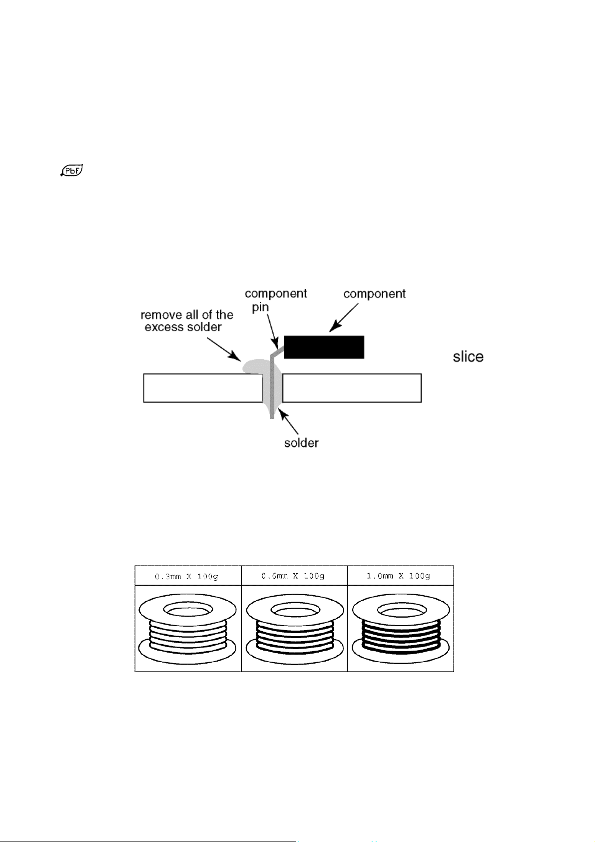
• After applying PbF solder to double layered boards, please check the component side for excess solder which may
flow onto the opposite side. (see Fig.3)
Fig.3
Suggested Pb free solder
There are several kinds of Pb free solder available for purchase. This product uses Sn+Ag+Cu (tin, silver, copper) solder.
However, Sn+Cu (tin, copper), Sn+Zn+Bi (tin, zinc, bismuth) solder can also be used. (see Fig.4)
Fig.4
6

Applicable signals
Signal name
525 (480)/60i 15,73 59,94
525 (480)/60p 31,47 59,94
625 (576)/50i 15,63 50,00
625 (576)/50p 31,25 50,00
750 (720)/60p 45,00 60,00
750 (720)/50p 37,50 50,00
1.125 (1.080)/60i 33,75 60,00
1.125 (1.080)/50i 28,13 50,00
640 x 400 @70 Hz 31,46 70,07
640 x 480 @60 Hz 31,47 59,94
640 x 480 @75 Hz 37,50 75,00
852 x 480 @60 Hz 31,47 59,94
800 x 600 @60 Hz 37,88 60,32
800 x 600 @75 Hz 46,88 75,00
800 x 600 @85 Hz 53,67 85,06
1.024 x 768 @60 Hz 48,36 60,00
1.024 x 768 @70 Hz 56,48 70,07
1.024 x 768 @75 Hz 60,02 75,03
1.024 x 768 @85 Hz 68,68 85,00
1.280 x 1024 @60 Hz 63,98 60,02
1.366 x 768 @60 Hz 48,36 60,00
Macintosh 13” (640 x 480) 35,00 66,67
Macintosh 16” (832 x 624) 49,72 74,54
Macintosh 21” (1.152 x 870) 68,68 75,06
Horizontal
frequency (kHz)
Vertical frequency
(Hz)
Conponent HDMI PC
∗∗
∗∗
∗∗
∗∗
∗∗
∗∗
∗∗
∗∗
∗
∗
∗
∗
∗
∗
∗
∗
∗
∗
∗
∗
∗
∗
∗
∗
Note:
• Signals other than above may not be displayed properly.
• Applicable input signal for PC is basically compatible to VESA standard timing.
• PC signal is magnified or compressed for display, so that it may not be possible to show fine detail.
7
Service Hints
How to remove the Pedestal assembly
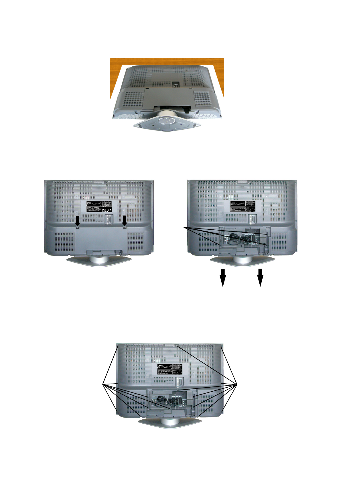
Lay the main unit face down. (see Fig.5)
Fig.5
Remove the cable cover. (see Fig.6)
Remove the 4 fixing screws and the pedestal assembly. (see Fig.7)
Fig.6
How to remove the backcover
Remove the cable cover. (see Fig.6)
Remove the 15 fixing screws. (see Fig.8)
SCREWS
SCREWS
Fig.7
SCREWS
Fig.8
8
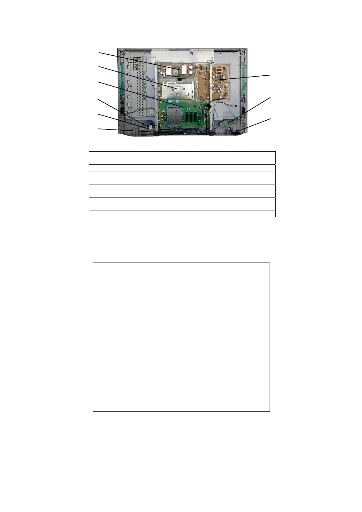
Chassis Board Layout
P-BOARD
DG-BOARD
H-BOARD
AP-BOARD
GS-BOARD
SD-MODULE
G-BOARD
Board Name Function
AP-Board Mains Input, Power Supply Regulator
DG-Board Global Core, HDMI
G-Board Local Key, Audio Amplifier
GS-Board SD Card Slot, SD Card Interface
H-Board AV Connector, TV tuner, AV Switch
K-Board Main Switch
P-Board DC Power Supply
SD-Module MPEG/JPEG interface
V-Board Remote Receiver, LED IR, Bats
Setting Inspection
Voltage Confirmation
AP board Normal mode
Test point Position Voltage
TP7201 Cathode D7102
TP7301 J218
TP7303 J415
TP7401 JS7958
TP7403 J213
TP7501 JS7503
TP7502 J221
TP7601 J406
TP7702 JS7702
V-BOARD
K-BOARD
Confirm the following voltages:
7V ± 1V
9V ± 0,45V
5,1V ± 0,25V
18,8V ± 0,8V
3,3V ± 0,15V
5,1V ± 0,25V
9V ± 0,45V
31,5V ± 2,5V
12,2V ± 0,6V
Standby mode
TP7201 Cathode D7102
TP7301 J218 max 2V
TP7303 J415 max 2V
TP7401 JS7958 max 2V
TP7403 J213 max 2V
TP7501 JS7503 max 2V
TP7502 J221 max 2V
TP7601 J406 max 4,5V
TP7702 JS7702 max 2V
10V ± 2V
9

Self Check
A
A
A
Self-check is used to automatically check the bus lines and hexadecimal code of the TV set. To enter Self-Check mode, keep
pressing the STATUS button on the remote control and press the down (-/v) button on the TV set. To exit Self Check,
switch off the TV set at the power button.
MEM O.K.
GC5 O.K.
GC3FS O.K.
VSW1 O.K.
VSW2 O.K.
TUN1 O.K.
VIF O.K.
MSP O.K.
SDM O.K.
HDMI O.K.
DV O.K.
TX-32LX600F TX-32LX600P TX-26LX600F TX-26LX600P
OPTION 1 4F 4F 4F 4F
OPTION 2 11 11 11 11
OPTION 3 3A 3A 3A 3A
OPTION 4 D9 59 D9 59
OPTION 5 EB EB 6B 6B
OPTION 6 AB AB AB AB
OPTION 7 00 00 00 00
OPTION 8 78 78 78 78
OPTION 9 00 00 00 00
OPTION 10 80 80 80 80
OPTION 11 C1 C1 C1 C1
OPTION 12 20 20 20 20
OPTION 13 20 20 20 20
CHECK 02 82 82 02
Display Ref. No. Description P.C.B.
MEM IC1102 EAROM DG-Board
GC5 IC4037 GLOBAL CORE DG-Board
GC3FS IC4020 GLOBAL CORE FOR SUB DG-Board
AVSW1 IC3005 AV SWITCH H-Board
AVSW2 IC2105 AV SWITCH H-Board
TUN1 TU3201
VIF TU3201 VIDEO INTERMEDIATE FREQUENCY H-Board
MSP IC2106 MAIN SOUND PROCESSOR H-Board
SDM SD-MODULE MPEG/PHOTO VIEW, SD RECORDING SD-MODULE
HDMI IC4026 HDMI I/F RECEIVER DG-Board
ADV IC4019 A/D CONVERTER DG-Board
If the CCU ports have been checked and found to be incorrect or not located then " - - " will appear in place of "O.K.".
MULTISTANDART SOUND
PROCESSOR
H-Board
10
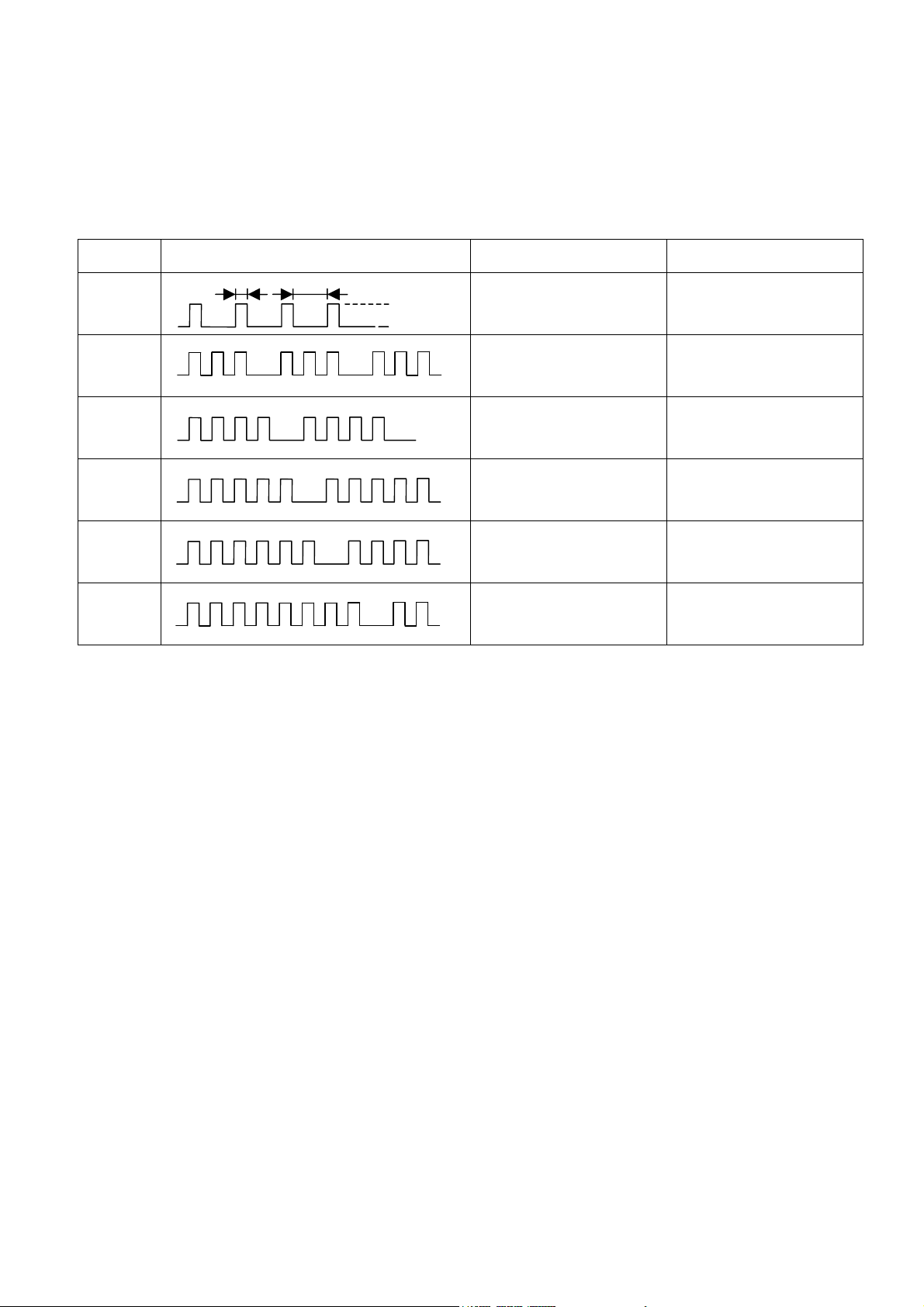
Power LED blinking timing chart
1. Subject
Information of LED Flashing timing chart.
2. Contents
When abnormality has occurred the unit, the protection circuit operates and reset to the stand by mode. At this time, the
defective block can be identified by number of blinking of the Power LED on the front panel of the unit.
Blinking
times
1 Inverter SOS
3
4 SUB 9V
5 SUB 5V
6 MAIN 9V AP BOARD, DG BOARD
8 MAIN 3,3V
Blinking timing Contents Check point
Once
4 sec
Light
No Light
BT_30V, SOUND 18V,
PANEL 12V
AP BOARD, H BOARD
AP BOARD, H BOARD
AP BOARD, H BOARD
AP BOARD, H BOARD
POWER UNIT
LCD PANEL
DG BOARD
DG BOARD
DG BOARD
11

Service Mode Function
MPU controls the functions switching for each IICs through IIC bus in this chassis. The following setting and adjustment can
be adjusted by remote control in Service Menu
How to enter SERVICE 1
In main menu, move to choose sound menu, set BASS to MAXIMUM, and set TREBLE to MINIMUM.
Simultaneously press INDEX button on remote control and DOWN button (-/v) on the TV set.
How to enter SERVICE 2
Enter the SERVICE 1 mode.
Press the GREEN button to step down to the last menu position.
Set the program position to 99.
Press HOLD button on remote control.
Note:
To exit from Service mode, press N or Power button on remote control.
12
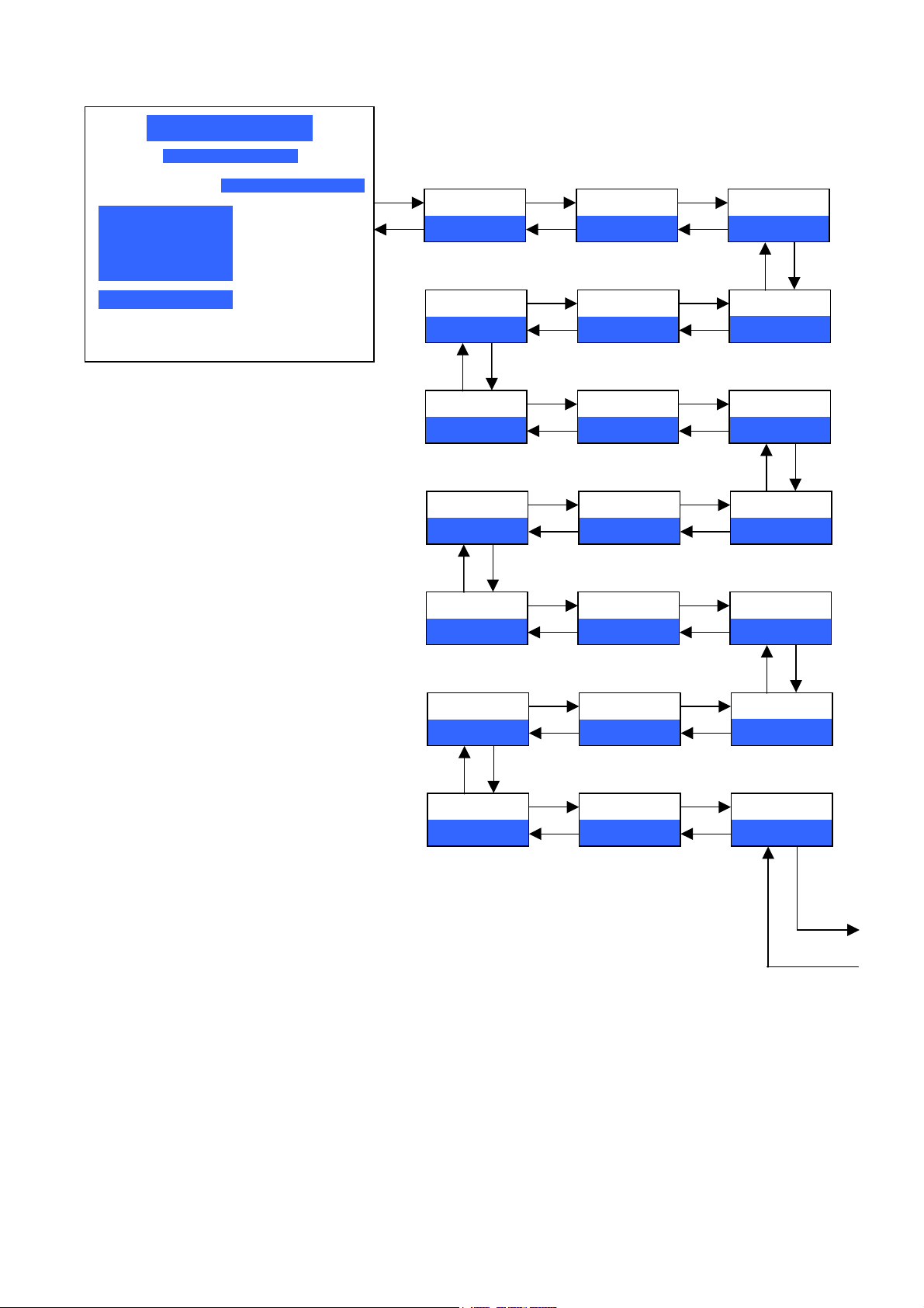
SERVICE 1
P A N A S O N I C 2 0 0 6 L C D
S e r v i c e 1
F l a s h P R O G R A M
E x t >> T V
S D >> T V
S D P R O G R A M
U p d a t e
O K t o p r o g r a m
V 1 . 02 0
S D ( R D – S D 0 0 8 ) : 1 0 5
[GREEN]
[RED]
Sub-Bright
2056
Sub-Backlight
479
[RED]
R-Gain
238
B-Cent
104
EQ 120Hz
EQ 7,5kHz
EQ 12kHz
0
-3
-3
[GREEN]
[RED]
[RED]
[GREEN]
[GREEN]
[GREEN]
[RED]
[RED]
[GREEN]
[GREEN]
[GREEN]
[RED]
[RED]
[GREEN]
[GREEN]
[GREEN]
[RED]
Sub-Contrast
640
Video Gain 2
216
G-Gain
255
G-Cent
128
EQ 200Hz
-3
EQ 3kHz
-3
CEC Check
OFF
[GREEN]
[RED]
[RED]
[GREEN]
[GREEN]
[RED]
[RED]
[GREEN]
[GREEN]
[RED]
[RED]
[GREEN]
[GREEN]
[RED]
Sub-Colour
43
[RED]
Sub-NTSC-Tint
254
B-Gain
240
[RED]
R-Cent
140
EQ 500Hz
0
[RED]
EQ 1,2kHz
1
SD Auto Check
Access
[GREEN]
[GREEN]
[GREEN]
13
[RED]
[RED]
[HOLD]
+Pos. 99
[INDEX]
+ Pos. 99
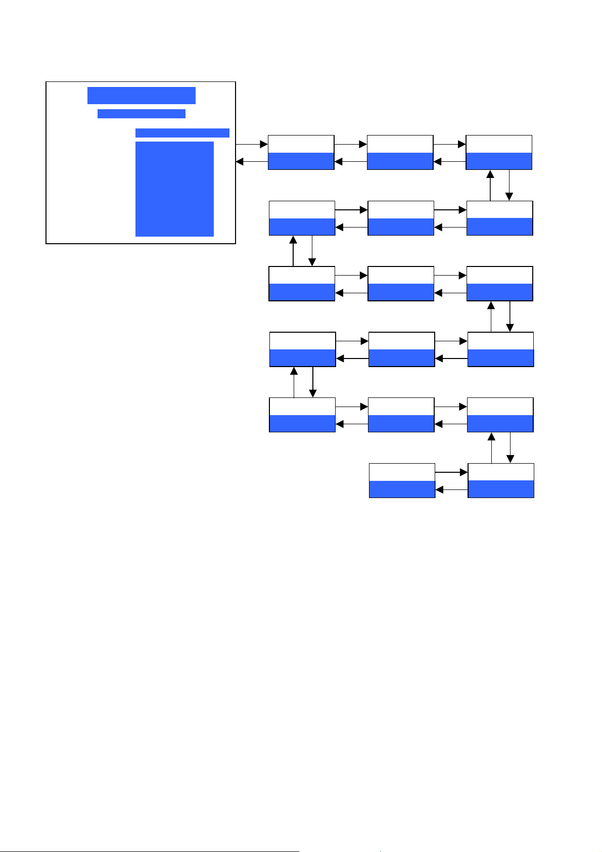
SERVICE 2
P A N A S O N I C 2 0 0 6 L C D
V 1 . 02 0
S e r v i c e 1
S D ( R D – S D 0 0 8 ) : 1 0 5
OPTION 1 : 4F
OPTION 2 : 11
OPTION 3 : 3A
OPTION 4 : D9
OPTION 5 : EB
OPTION 6 : AB
OPTION 7 : 00
OPTION 8 : 78
OPTION 9 : 00
OPTION 10 : 80
OPTION 11 : C1
OPTION 12 : 20
OPTION 13 : 20
Key Command
• Press the RED/GREEN button to step
up/down through the functions and
adjustments.
• Press the YELLOW/BLUE button to
change the adjustment values or function.
• Press the numerical button 1-7 to change
0/1 of each option item.
• Press the OK button after each adjustment
has been made to store the required
values.
[GREEN]
[RED]
Y/C Delay
2
OPTION 5 (EB)
1 1 1 0 1 0 1 1
[RED]
OPTION 6 (AB)
1 0 1 0 1 0 1 1
OPTION 11 (C1)
1 1 0 0 0 0 0 1
OPTION 12 (20)
0 0 1 0 0 0 0 0
[GREEN]
[RED]
[RED]
[GREEN]
[GREEN]
[GREEN]
[RED]
[RED]
[GREEN]
[GREEN]
[GREEN]
[RED]
OPTION 1 (4F)
0 1 0 0 1 1 1 1
OPTION 4 (D9)
1 1 0 1 1 0 0 1
OPTION 7 (00)
0 0 0 0 0 0 0 0
OPTION 10 (80)
1 0 0 0 0 0 0 0
OPTION 13 (20)
0 0 1 0 0 0 0 0
Hours
00020
[GREEN]
[RED]
[RED]
[GREEN]
[GREEN]
[RED]
[RED]
[GREEN]
[GREEN]
[RED]
[RED]
[GREEN]
OPTION 2 (11)
0 0 0 1 0 0 0 1
[RED]
OPTION 3 (3A)
0 0 1 1 1 0 1 0
OPTION 8 (78)
0 1 1 1 1 0 0 0
[RED]
OPTION 9 (00)
0 0 0 0 0 0 0 0
H-Pos
0
[RED]
V-Pos
0
[GREEN]
[GREEN]
[GREEN]
14

Option Description
option1
b0 Auto (1)
Colour system
b1 SECAM (1)
b2 NTSC (1)
b3
b4 A2 select 6,5MHz 5,742MHz (0) 6,742MHz (1)
b5b6SIF I only (0), BG only (1)
b7 free
option2
b0 enable (1)
A2 enable
b1 not use
b2 not use
b3
b4 enable (1)
NICAM enable
b5 not use
b6 not use
b7
option3
b0 SASO enable SASO enable (1)
b1 Fine tuning Enable (1)
b2 Search speed Slow (1), Fast (0)
b3 Tuner MACO Tuner (1), Others (0)
b4 HYPER UHF only (0), UHF/VHF (1)
b5 IF I2C I2C controlled Tuner IF module (1)
b6 NICAM C4 bit enable (1)
b7 Blue Back BLUE BACK on/off selection in menu (0)
option4
b0 Aspect AUTO enable (1)
b1 S1/S2 enable enable (1)
b2 ID-1 enable (1)
b3 User aspect Just enable (1)
b4 User aspect 14:9 enable (1)
b5 ALBD 14:9 14:9 enable, Zoom3 disable at self wide (1)/Zoom1, Zoom3 enable at self wide (0)
b6 TEXT enable (1)
b7 TEXT TOP TOP enable (1)
option5
b0 CH Blanking Blanking enable (1)
b1 AV Blanking Blanking enable (1)
b2 Noise mute Noise mute enable (0)
b3 sub picture without sub-picture (0), with sub-picture (1)
b4 2tuner 2tuner (1), 1tuner (0)
b5 AV input 3rotation (1)/2rotation without front RCA (0)
b6 Panel (LCD) HITACHI Panel (1)/LG Panel (0)
b7 Large size (LCD) 32 (1)/26 (0) for LCD
option6
b0 SD module with SD module (1)
b1 SD module Ext. Rec(PAL) enable (1)
b2 SD module Ext. Rec(NTSC) enable (1)
SD module Ext. Rec(SECAM)
b3
b4 IDTV enable (1)
b5 HDMI enable (1)
b6 Ext. HV input Without HV input (0)/ with HV input (1)
b7 PC enable (1)
option7 Area option
b0 Asia Asia (1), Europe (0)
b1 Australia not use
b2 Ireland/India Ireland (1)
b3 UK/Korea UK (1)
b4 Lang1 not use
b5 Lang2 not use
b6 Lower POS not use
b7 Owner ID not use
M.NTSC (1)
I/BG/DK/L (2), BG/DK (3)
not use
not use
enable (1)
15

option8 Euro option
b0 ACI all country ACI enable (1), only Netherlands (0)
b1 ACI auto MP ACI auto multi package enable (1)
b2 ACI offset ACI offset for VCR prog. enable (1)
b3 Power up EC-Mode Power on EC enable (1)
b4 AVLink Q-Link off selectable in menu (1)
b5 Volume correction TV Volume correction enable (1)
b6 MPX/NICAM display Display NICAM (0), Display MPX (1)
b7 Albd Reset Off enable (1)
option9 Asia option1
b0 ASIA / M.E. / HK / UK / CHINA (1)
CH Plan
b1 NZ/ INDNES (1)
b2 AUSTRALIA (1)
b3 E.EUROPE (1)
b4 SPECIAL (1)
b5 AMERICA (1)
b6 CATV (1)
b7
option10 Asia option2
b0 ASIA / M.E. (1)
NICAM priority
b1 HK / UK (1)
b2 CHINA (1)
b3 NZ / INDN (1)
b4 AUSTRA (1)
b5 E.EURO (1)
b6
b7 HDMI AVI Aspect enable (1)
option11 Additional
b0 Remocon Type Delux (1), Leader (0)
b1 Environment AI (PDP) Enable with viewing mode auto (1)/ disable without viewing mode auto (0)
b2 WSS 14:9 off WSS 14:9 off (1)
b3 Child lock Child Lock Tuning Menu skip (1)
b4
b5 Contrast AI enable (1) LCD only
b6 Service H-POS enable (1)
b7 Service V-POS enable (1)
option12 Additional
b0
b1
b2
b3
b4
b5 SRS enable (1)
b6
b7
option13 Additional
b0
b1
b2
b3
b4
b5 FTZ enable (1)
b6
b7
JAPAN (1)
SPECIAL (1)
16

Adjustment Method
Sub-Contrast/White Balance Adjustment
Instrument Name Connect to Remarks
1. Remote controller
2. LCD WB meter (Minolta CS-1000A equivalent)
3. Comunication jig
4. Computer for external control
Procedure Remarks
Subcontrast adjustment
1. Receive PAL colour bar (100% white) RF signal.
2. Enter “Sub-Contrast” adj. In SERVICE 1 mode.
3. Start adjusting by using Blue Key.
4. If the adjustment finished normally, the letter of “Sub-Contrast” will change
from red to black
White Balance adjustment
1. Procedure basically perform checking using the production software and make
automatic adjustment using external computer.
2. It adjust in the mode of Colour balance Normal as follows.
TX-32LX600F, TX-32LX600P TX-26LX600F, TX-26LX600P
TOP Normal TOP Normal
x: 0,2800 ± 0,003 x: 0,2800 ± 0,003
y: 0,2850 ± 0,003 y: 0,2850 ± 0,003
Correlation can be also taken by
CA-210 or equivalent
Let the panel standfor more than 3
hours at more than 20 °C.
Basically perform adjustment in the
ambient environment of room
temperature more than 20 °C.
The aging time is more than20 min
at above room temperature.
Applied signal
100% full colour bar
0,7V p-p white peak
87.5% modulation
GRAY Normal GRAY Normal
x: 0,2800 ± 0,003 x: 0,2800 ± 0,003
y: 0,2850 ± 0,003 y: 0,2850 ± 0,003
The address of EEPROM to write is as follows
Add. C148-C159
17
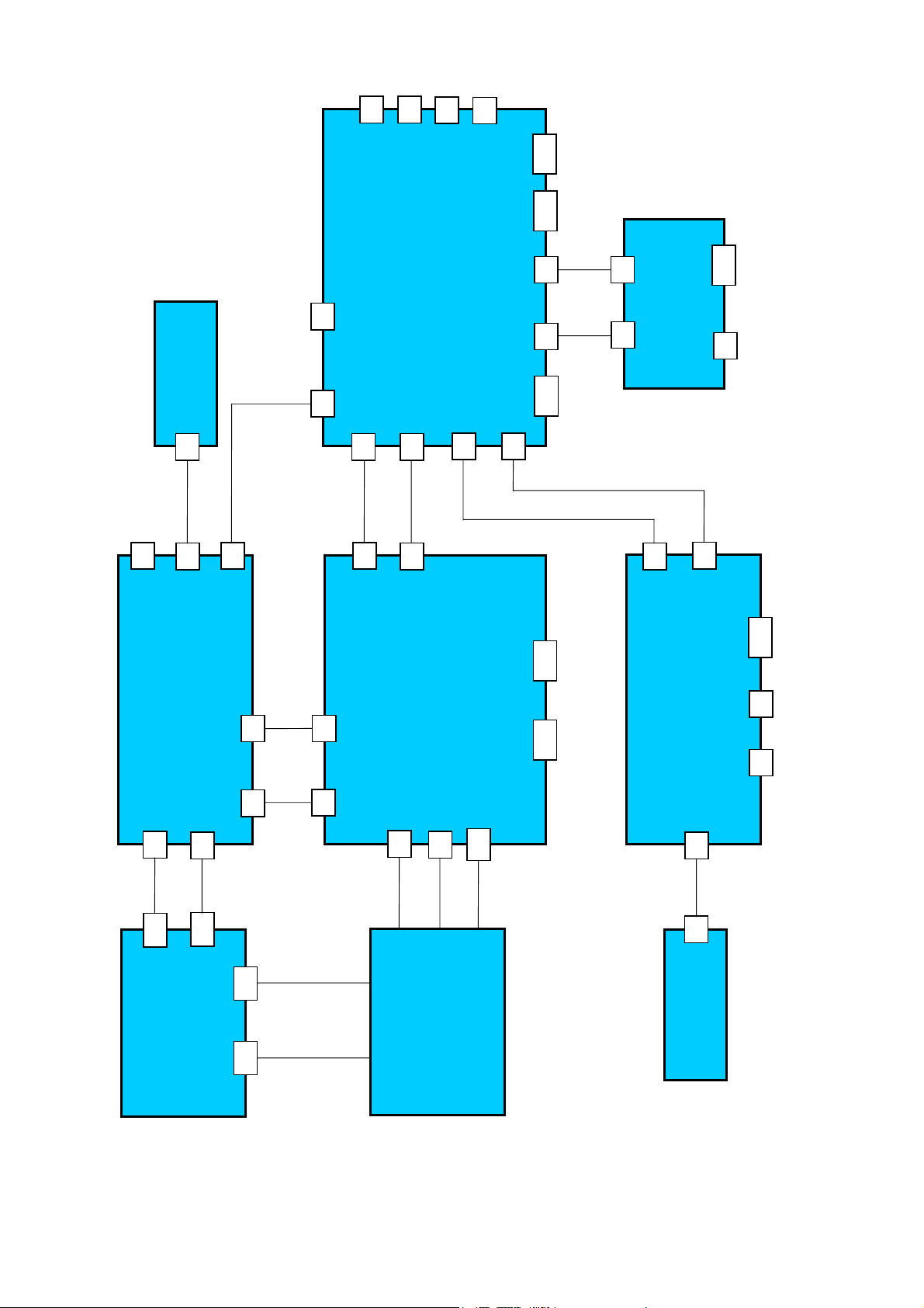
Wiring diagram
AV1
AV2
AV3
AV3C
OUT
JK2001
PC AUDIO
PC IN
JK3001
H8H9
GS8
SLOT
JK6701
SD CARD
H-BOARD
H12
SERVICE
K-BOARD
K6
MAINS IN
AP1
AP6
AP10
AP-BOARD
H1
DG5
H2
DG2
H3
DG3
DG-BOARD
H4
H5
JK2002
HDMI2
HDMI1
UDIO
OUT
GS9
GS-BOARD
G4
G5
G-BOARD
GS3
SD
MODULE
JK3801
G10 G11
V4
FRONT
SP-R
SP-L
AP3
CN201
P-BOARD
AP2
CN101
AP4 AP 5
CN203
CN202
DG4
26” models only
DG6
DG7
LCD PANEL
DG11
32” models only
G1
V1
V-BOARD

V
Video & Stereo Audio Block Diagram
V
Y
V
AV1_VOUT 19
AV1_RED 15
AV1_GREEN 11
AV1_BLUE 7
AV1_LOUT 3
V1 21PIN SCART
AV1_ROUT 1
AV2_VOUT 19
AV2_LOUT 3
AV2_ROUT 1
AV2 21PIN SCART
AV3_VOUT 19
AV3_RED/C 15
AV3_GREEN 11
AV3_BLUE 7
AV3_LOUT 3
V3 21PIN SCART
AV3_ROUT 1
AV3C
PC AUDIO IN
R
L
JK3801
AV4 FRONT
H-BOARD
AV1_V 20
AV1_L 6
AV1_R 2
AV2_V 20
AV2_C 15
AV2_L 6
AV2_R 2
AV3_V 20
AV3_L 6
AV3_R 2
Y
PB
PR
L
JK2001
R
G-BOARD
C
Y
R
L
GUARD_SR
GUARD_SL
GUARD_V
GUARD_C
GUARD_Y
GUARD_SR
GUARD_SL
Q3002
Q2009
Q2010
TUNER
AV4_R
AV4_L
H4
G4
SIF_OUT
14
17
Q2006
Q2007
Q2003
Q2004
HP_R
HP_L
222629
30
222629
30
V4_C
14
14
Q3004
Q3003
1 AV1_L
23 AV1_LO
2 AV1_R
24 AV1_RO
3 AV2_L
27 AV2_LO
4 AV2_R
28 AV2_RO
8 AV3_L
30 AV3_LO
9 AV3_R
31 AV3_RO
16 PC_LIN
17 PC_RIN
AV4_Y
11
11
Q3203
Q3202
AV4_
7
7
MSP
Q2108 Q2106
MAIN_RFVIDEO_OUT
Q3010
53 AV1_V
51 AV1_VO
19 AV1_RED
17 AV1_GREEN
20 AV1_BLUE
58, 59 AV2_V
38 AV2_VO
61 AV2_C
29 AV3C_PB
VIDEO SWITCH
3, 4 AV3_V
37 AV3_VO
6, 24 AV3_RED/C
22 AV3_GREEN
25 AV3_BLUE
27 AV3C_Y
30 AV3C_PR
IC2105
AUDIO SWITCH
25 SD_AUDIO_L_OUT
26 SD_AUDIO_R_OUT
SQ_L
4
IC2500
AUDIO
AMPLIF IER
13
16
SQ_L+
1
G10
IC3005
HDMI_R
HDMI_R 11
19 SD_MONO_IN_R
SQ_L-
2
HDMI_L
10
HDMI_L
18 SD_MONO_IN_L
MAIN_RF_CVBS 14
MAIN_CY/Y/V/G
TV_L
TV_R 15
MAIN_L 32
MAIN_R 33
AV4_L
AV4_R
WF_L
IC2501
AUDIO
AMPLIF IER
16
oo_L+
Woo_L-
3
4
MAIN_PB/C/R 49
MAIN_PR/B 48
VOUT5 42
SUB_CY/Y/V 46
SUB_PB/C 45
SUB_PR
SD_VIN 13
SD_REC_V 41
AV4_V 63
AV4_Y
AV4_C
14
6
7
4
13
50
44
64
1
34 TV_ L
33 TV_R
56 MAIN_ L
57 MAIN_ R
3
IC2101
HP AMPLIFIER
1
HP_R
IC2502
AMPLIF IER
16
AUDIO OUT
JK2002
L
ANA_IN1+ 67
SC1_OUT_L 37
SC1_OUT_R 36
24 HEADPHONE R
5
7
HP_L
SQ_R
4
AUDIO
13
SQ_R+
1
G11
PC AUDIO IN
R
SPEAKER_ L 28
SPEAKER_ R 27
IC2106
AUDIO
PROCESSOR
25 HEADPHONE L
IC2303
AMPLIF IER
7
SK_L
H5
G5
IC2503
AMPLIF IER
16
oo_R+
SQ_R-
3
2
JK3001
2
1
Q2105
Q2104
62
AUDIO
1
SK_R
17
13
11
17
11
13
WF_R
4
AUDIO
13
Woo_R-
4
3
Q3331
Q3333
SD_AUDIO_R_OUT
19
19
Q3332
MAIN_CY/Y/V/G _OUT
Q3014
Q3017
Q3011
Q3015
MAIN_PB/C/R _OUT
MAIN_CVBS _OUT
SUB_CY/Y/V _OUT
53
IC2104
AUDIO
AMPLIF IER
7
1
L_OUT
R_OUT
62
IC2302
AUDIO
AMPLIF IER
1
7
WF_L
WF_R
SD_MONO_IN_L
SD_MONO_IN_R
SD_AUDIO_L_OUT
H9
GS9
GS-BOARD
PC_B
PC_G
PC_R
HDMI_R
HDMI_L
MAIN_PR/B _OUT
SUB_PB/C _OUT
SUB_PR _OUT
5
7
9
3
9
357
H2
18
20
16
30
28
H3
1
3
5
7
11
13
15
SD_V_IN
SD_REC_
15
11
11
15
SD CARD
JK6701
DG2
23
21
25
11
13
DG3
40
38
36
34
30
28
26
DG-BOARD
THIS IS EXCHANGE UNIT
PC_B
PC_G
PC_R
HDMI_R
HDMI_L
MAIN_CY/Y/V/G
MAIN_PB/C
MAIN_PR
RGB_CVBS
SUB_Y
SUB_PB
SUB_PR
8Bit data
Q4040
Q4041
Q4042
HDMI 1
8Bit data
HDMI 2
SD V_IN
SD L_OUT
SD L_IN
SD R_IN
GS3
6
12
16
14
20
18
SD V_OUT
SD R_OUT
Q4043
Q4044
Q4052
Q4051
VIN1 30
VIN2 35
VCLP 44
IC4020
GC3FS-S
39,40,43,44
47,48,51,52
IC4026
C1AB00002535
HDMI I/F
58,59,62,63,
66,67,70,71
SD MODULE
OCLP 43
MCLK 88
SCK 86
Q4046
Q4054
VIN3 40
SDO 84
WS 85
56 PC_B
54,52 PC_G
58 PC_R
7
IC4028
AMP
1
6
2
Q4059
Q4050 Q4058
Q4081 Q4057
Q4056
Q4080
Q4055
Q4053
CVBS0
MCU
EURO TEXT
HDMI_R_AUDIO
HDMI_L_AUDIO
10 11
IC4025
AUDIO DAC
2
4
3
1
WS
SCK
SDO
MCLK
YCLP 45
HDMI_Y0-Y7, HDMI_UV0-UV7
HDMI_VS
HDMI_HS
HDMI_OE
REFCK_HDMI
UBIN2-UBIN9, YBIN2-YBIN9
CLK, VSIB, HSIB
ANALOG
VIDEO
CVBS1
IC4019
ADV7499B
77 RESET
76 YIN
74 PB/C
72 PR
57 RGB_CVBS
142
MICROPROCESSOR
151
PORT B (FS&HDMI)
IC1103
2,3,4,6,7,8,10,11,12,14,15,16,18,19,20,22, 23,24,
27,28,30,31,50,51,52,54,55,56
37 42
RX0-
6
DG7
PORT A (ADV7499)
IN0-YIN9, UVIN0-UVIN9
CLK, VSIA, HSIA, REFCK_ADV
PORT D-OSD INPUT
IC4037 – GC5
MNA84522-A
B0E2-B0E9, G0E2-G0E9, R0E2-R0E9
VS0E, HS0E, CLK0E, LVDS-ENB
PORT E
IC4040
LVDS TRANSMITTER
46
38
RX0+
7
39 40
RX1-
9
RX1+
45
41
RX2-
10
RXCLK+
RXCLK-
RX2+
15
11
16
13
47
RX3-
48
RX3+
19
18
TO LCD PANEL
r
CO
V
V
V
V
V
A
A
A
A
V
A
A
A
A
V
V
V
SLOT
26÷31
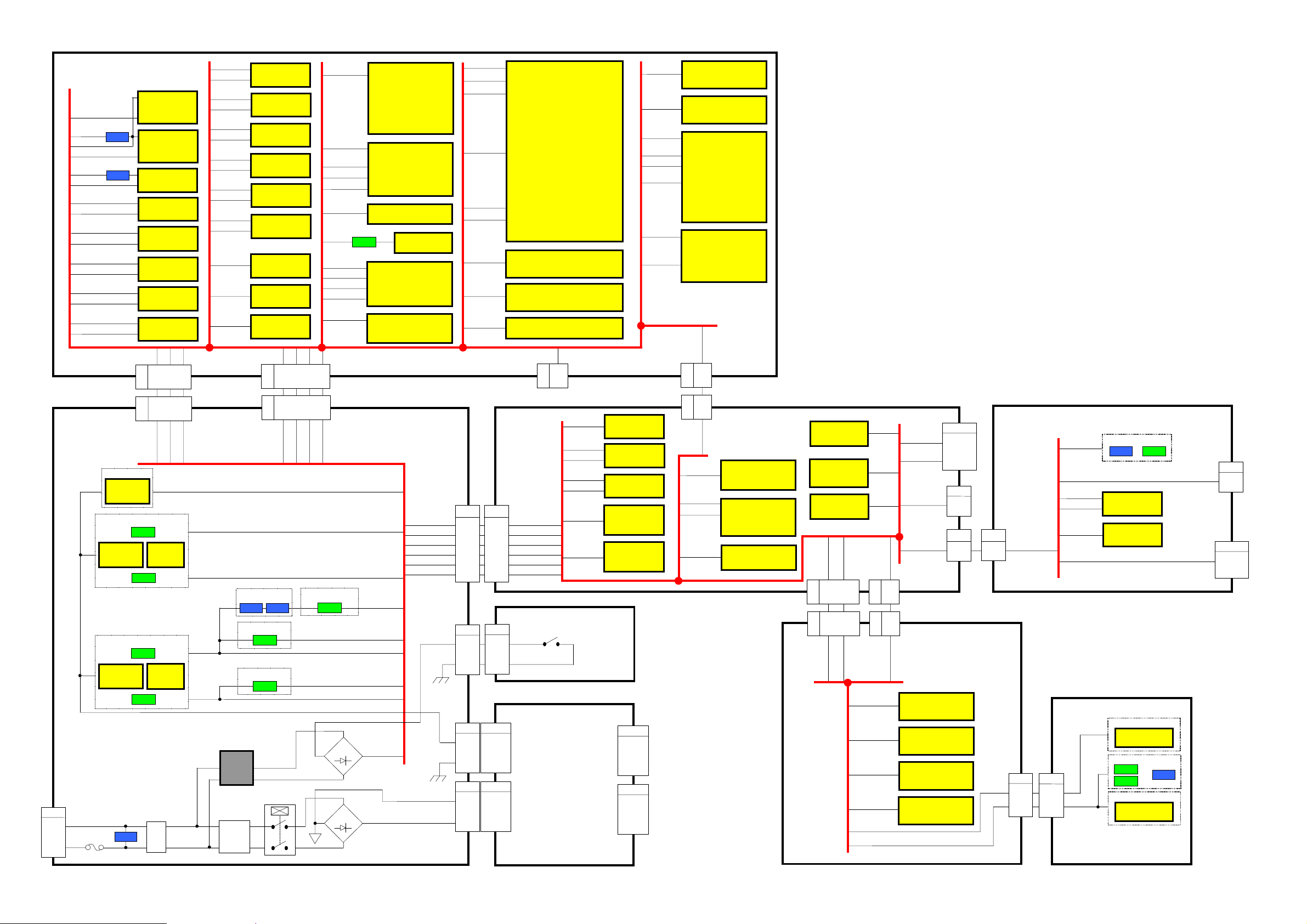
Power Supply Block Diagram
DG - BOARD
THIS IS EXCHANGE
STB_1,5V
SUB_5V
STB_7V
STB_3,3V
MAIN_5V
ADV_3,3V
MAIN_3,3V
AD_2,5 V
MAIN_3,3V
1,8V
MAIN_3,3V
PLL_2,5V
MAIN_3,3V
1,8V 1
MAIN_3,3V
MAIN_1,8V
AP - BOARD
24V
AP10
1
F7000
2
MAINS IN
UNIT
PANEL Vcc
IC7701
REGULATOR
MAIN DC/DC
IC7402
COMPARATOR
SUB DC/DC
IC7302
COMPARATOR
4 Vin
5 Vout
4 Vin
5 Vout
8 Vin
1 Vout
1 VDD
5 Vout
1 VDD
5 Vout
1 VDD
5 Vout
1 VDD
5 Vout
7 Vin
1 Vout
DG5
AP5
Q7402
Q7401
Q7302
Q7301
LF7002
IC1110
REGULATOR
IC1108
REGULATOR
IC4013
REGULATOR
IC4014
REGULATOR
IC4016
REGULATOR
IC4017
REGULATOR
IC4018
REGULATOR
IC4027
REGULATOR
2÷4
2÷4
STB_7
SUB_5
IC7401
PS
NTROL
IC7301
PS
Line
Filte
MAIN_3,3V
2,5V
MAIN_5V
PLL_3,3V
MAIN_5V
3,3V
MAIN_3,3V
DDR_2,5V
MAIN_3,3V
MAIN_2,5V
SUB_9V
MAIN_1,2V
MAIN_9V
MAIN_5V
STB_7V
7
22÷23
5 Vin
IC4029
REGULATOR
4 Vout
5 Vin
IC4030
REGULATOR
4 Vout
5 Vin
IC4031
REGULATOR
4 Vout
2 Vcc
IC4044
REGULATOR
4 Vout
1 VDD
IC4045
REGULATOR
5 Vout
1 Vin
IC4046
REGULATOR
2 Vout
IC4028
8
OP AMP
IC4025
14
D/A CONVERTER
IC1109
2
RESET IC
DG4
DDR_2,5V
MAIN_3,3V
AD_2,5V
MAIN_2,5V
PLL_2,5V
STB_3,3V
STB_7V
ADV_3,3V
MAIN_3,3V
1,8V 1
1,8V
MAIN_3,3V
3÷4
8÷10
20÷22
13÷14
C6, C7, D3, D10, K3, K6,
K7, K10, B3, B2, B4, B6,
B7, B9, B10, B11, D2, D11,
E3, E10, F3, F10, H3, H10,
J3, J10, G3, G10
IC4038
DDR SDRAM
6, 12, 17, 51,
62, 69, 81, 97
28, 33, 38, 41
8, 15, 53, 66, 82, 95
49, 57
ANALOG SWITC H
5V
14
TRANSMITTER
IC1106
ANALOG SWITC H
IC4019
ADV7499B
IC4040
Q1148
14
63
6, 18
12, 39, 90
47,48
1, 9, 26,
34, 44
IC4020
GC3FS-S
IC1107
LVDS
2,5V
PLL_3,3V
MAIN_3,3V
MAIN_1,2V
3,3V
DDR_2,5V
STB_3,3V
STB_3,3V
STB_3,3V
AF6, AC4 , AG5, AG14,
W15
AA26, AB26, AK26, D11, D15,
D19, D20, E7, E8, E11, E12, E15,
E16, E19, E20, E23, E24, F26, F27,
J26, J27, K5, K26, K27, L5, M18,
M19, N18, N19, N26, N27, W5, P4,
P5, P26, P27, R4, R5, U26, U27,
V5, V26, V27, AF19, AF18
EAROM
PANEL_12V
IC4037
GC5
AE26, AE 27, AF26, AF27,
AG27, AH 28, AJ 29, AK3 0,
B1, C2, D3, E4, F5, M12,
M13, M14, N12, N13, N14,
P12, P13, P14, R15, T16,
T17, T18, T19, U17, U18,
U19, V18, V19, W18, W19
AF22, AK20
AA1, AA2, AB2, AB3, AB4, AB5,
AF7, AF10, AF1 1, AG6, AG7, AG 10,
AG11, AJ1, V12, V13, W12, W13,
1, 3, 9, 14,
27, 43, 49
37
8
IC1100
64MBIT SDRAM
IC1101
FLASH MEMORY
IC1102
DG7
MAIN_5V
MAIN_5V
MAIN_3,3V
MAIN_3,3V
MAIN_3,3V
MAIN_1,8V
STB_1,5V
STB_3,3V
IC4023
8
2KBIT EEPROM
IC4022
8
2KBIT EEPROM
5, 26, 76, 89, 98,
109, 122, 134,
6, 7, 13, 16, 19
38, 42, 46, 50, 57,
61, 65, 69
22, 23, 35, 74, 79, 92,
94, 105, 114, 128, 139
IC4026
HDMI RECEIVER
55, 98, 137,
182, 204
16, 30, 49, 73,
88, 108, 129,
154, 170, 191,
201, 214
DG3
IC1103
MICRO
PROCESSOR
STB_3,3V
14
TO LCD PANEL
7
22÷23
MAIN_5
UNREG_30V
AP4
3÷4
8÷10
20÷22
13÷14
SUB_9V
MAIN_9
MAIN_3,3V
PANEL_12
BT_30V
Q7601
PANEL_12V
SOUND_16V
MAIN_3,3V
BT_30V
SOUND_16V
MAIN_5V
SUB_5V
SUB_9V
MAIN_3,3V
BT_30V
AP1
7-9
11
15
17÷18
21
23
H - BOARD
H1
7-9
11
15
17÷18
21
23
SOUND_16V
MAIN_5V
SUB_5V
SUB_9V
MAIN_3,3V
BT_30V
MAIN_5V
SUB_9V
8V
SUB_9V
5V
SUB_9V
MAIN_3,3V
8
3 Vin
1 Vout
1 Vin
3 Vout
8
8
IC2101
HP AMPLIFIER
IC2103
REGULATOR
IC2107
REGULATOR
IC2104
UDIO
MPLIFIER
IC3301
DUAL
BUFFER
K - BOARD
SUB_9V
SUB_5V
T7101
238
L7001
3
PFC
Filter
2
MAIN_9V
Q7501
MAIN_5V
Q7504
7
RL7001
4
1
MAIN_SW_ON
D7102-5
-
D7004
-
MAIN_9V
SUB_9V
MAIN_5V
SUB_5V
24V
~
STB_7V
+
~
~
+
~
AP6
1
2
AP3
1÷4
5÷9
AP2
1
3
K6
1
2
POWER UNIT
CN201
1÷4
5÷9
CN101
1
3
SW001
THIS IS
EXCHANGE
UNIT
CN202
CN203
TO LCD PANEL
H3
SUB_9V
8V
5V
SUB_9V
27
GS - BOARD
TUNER
SERVICE
GS9
1
SUB_5V
G1
2
5
SUB_5V
SUB_5V
SUB_5V
3,3V
3,3V
3,3V
V - BOARD
V1
2
STB_3,3V
5
SUB_5V
SD LED
Q6702
1, 5 Vin
IC6701
4 Vout
REGULATOR
IC6703
14
BUS BUFFER
CATS
PC1001
PHOTO COUPLER
R&G LED
Q1003
Q1004
REMOTE CONTROL
RM1001
LED RECEIVER
GS3
38-40
TO SD MODULE
JK6701
4
SD CARD
IC2303
UDIO
STB_3,3V
IC2105
5
UDIO
SWITCH
39
IC2106
12, 13,
65, 66,
80
8
UDIO
PROCESSOR
IC2302
UDIO
MPLIFIER
MPLIFIER
IC3005
IDEO
SWITCH
IC2108
RESET IC
SUB_5
2
H4
2
G4
SUB_5V
8
7, 39
STB_3,3
19
19
STB_3,3V
SOUND_16V
SOUND_16V
SOUND_16V
SOUND_16V
SUB_5V
STB_3,3V
SUB_9V
SUB_9V
2
H5
G5
5V
SOUND_16
1÷5
1÷5
SOUND_16V
5, 18
5, 18
5, 18
5, 18
TU3201
SUB_5V
BT_30V
MAIN_5V
SUB_5V
IC2500
AUDIO AMPLIFIER
IC2501
AUDIO AMPLIFIER
IC2502
AUDIO AMPLIFIER
IC2503
AUDIO AMPLIFIER
2÷3
15
H12
1
H9
1
G - BOARD
A
A
A
V
2
A
A
A
A
A
Y
V
A
A
A
A
A
A
X
A
A
A
A
K
V
V8V
V
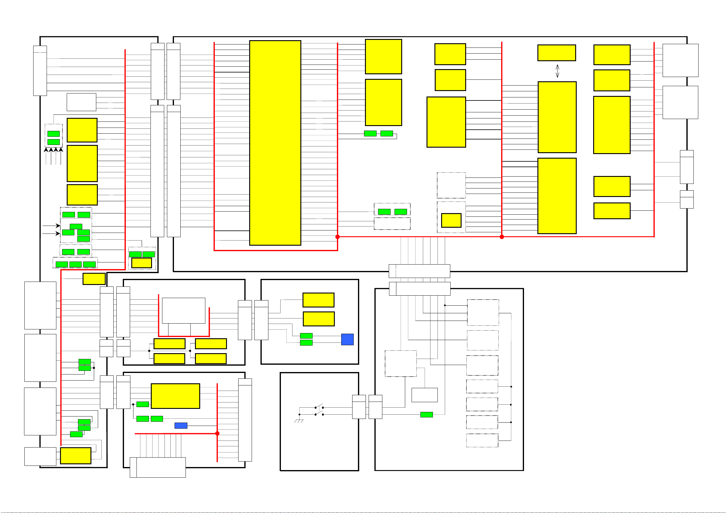
Control Block Diagram
H - BOARD
H12
2
4
5
SERVICE
6
7
MAIN_5V
SUB_5V
AV1_SLOW 8
SCL2 10
SDA2 12
AV1_FB 16
AV1 21 PIN SCART
AV2_QLINK 10
AV2_SLOW 8
AV2 21 PIN SCART
AV3_FB 16
AV3_QLINK 10
AV3_SLOW 8
AV3 21 PIN SCART
PC IN
SRQ
SD_TXD0
SD_RXD0
SCL3
SDA3
SOS
Q3008
Q3009
5
MAIN_5
HD 13
VD 14
TUNER
IC2105
AUDIO
SWITCH
IC3005
SUB_9
SWITCH
IC2106
PROCESSOR
MUTE
Q2123
HW_MUTE
Q2011
Q2017 Q2018
AUDIO OUT MUTE
Q2001
AV1-2-3 OUT MUTE
Q2120
Q2119
MSP_RESET
TIMER_REC_LED
AV1_FB
AV3_FB
O1
FB
SDA3
SCL3
SCL2
SDA2
O2
Q3001
VD
HD
5
IC3301
DUAL
2
BUFFER
IDEO
AUDIO
Q2124
Q2016
Q2002
AI_SENSOR
Q3016
Q3019
Q3005
Q3006
12
11
10
35
36
37
22
35
36
31
52
57
23
2
3
21
Q2121
IC2108
4
RESET IC
KEYSCAN
RMCN
R_LED
KEY_EDGE
G_LED
SP_MUTE
SD_RX
SD_TX
SD_IRQ
SD_RST
3
6
SD_TXD0
SD_RXD0
SCL3
SDA3
AFC1
SDA2
SCL2
SOS2
SDA2
SDA2
AV1_SLOW
AV2_SLOW
AV3_SLOW
SDA2
MSP_RESET
MUTE
MUTE_OUT
HP_MUTE
SP_MUTE
MUTE_OUT
MUTE_OUT
H4
21
20
17
16
8
4
1
H5
15
H8
1
3
5
7
SRQ
SCL2
O2
O1
SCL2
FB
SCL2
G4
21
20
17
16
8
4
1
G5
15
GS8
1
3
5
7
G_LED
SD_RX
SD_TX
SD_TIMER_LED
SD_RST
SD_IRQ
AV2_QLINK
AV3_QLINK
RMCN
AI_SENSOR
AFC1
MSP_RESET
KEYSCAN
SRQ
SOS2
MUTE
R_LED
KEY_EDGE
SDA1
SCL1
SDA2
SCL2
SDA3
SCL3
HP_MUTE
HP MUTE
Q2115
Q2114
IC2101
HP AMP
G - BOARD
KEYSCAN
REMOTE
R_LED
AI_SENSE
TIMER_REC_LED
KEY_EDGE
G_LED
MUTE
GS - BOARD
Q6701
Q6704 Q6703
SD_WP
12
H2
27
26
25
24
23
22
HD
14
VD
12
H3
40
39
38
36
35
34
33
32
31
30
26
25
24
23
21
20
18
17
FB
9
7
7
3 SD_RX
5 SD_TX
8 SD_IRQ
1, 4, 10,13 SD_RST
SD_DATA1
SD_CD
SD_DATA2
9
DG2
14
15
16
17
18
19
27
29
DG3
1
2
3
5
6
7
8
9
10
11
15
16
17
18
20
21
23
24
32
LOCAL KEYS
SWITCHING
KEY_EDGE
IC2500
AUDIO AMP
IC2501
AUDIO AMP
IC6703
BUFFER
SD_CMD
SD_CLK
SD-DATA0
5
7108
DG - BOARD
G_LED
SD_RXD
SD_TXD
SD_TIMER_LED
SD_RST
SD_IRQ
PC_HS
PC_VS
AV2_QLINK
AV3_QLINK
RM_IN
AI_SENSOR
AFC1
MSP_RESET
KEY1
SRQ
SOS
AUDIO_MUTE
R_LED_STBY_LED
KEY_EDGE
SDA1
SCL1
SDA2 (SDA0B)
SCL2 (SCL0B)
SDA3 (SDA0A)
SCL3 (SCL0A)
RGB_FB
INVERTER_ON
VIDEO_MUTE
LVDS_PD
PANEL_VCC_ON
PWM_POWER_ON
AQ_D0÷ AQ_D15
AR_LDQ M
AR_UDQM
AR_CLK
AR_CKE
AR_WR
AR_CAS
R_RAS
R_CS
R_BA0
AO_A0
MEMA 10
CEC
AUDIO_MUTE
WP
R_LED_STBY_LED
G_LED
MSP_RESET
SD_RXD
SD_TXD
GC_RST
SD_TIMER_LED
AO_A16 ÷AO_A8,
AO_A19 , AP_WE ,
AO_A18 , AO_A1 7,
AO_A7÷ AO_A5,
AO_A4÷ AO_A1
SD_IRQ
THIS IS EXCHANGE UNIT
IC2502
AUDIO AMP
IC2503
AUDIO AMP
IO0
RXD
TXD
RESET
LED_SD
AI_SENSE
SD_DATA3
SD_DATA2
SD_DATA1
SD_DATA0
MATRIX
SD_DATA3
1
KEYSCAN
IO0
RXD 6
TXD 2
7
7
9
REMOTE
R_LED
G_LED
IO0
RESET
RXD
TXD
LED_SD
SD_WP
SD_CD
SD_CMD
SD_CLK
1
2
3
4
5
8÷15, 23÷26, 17÷20
27
28
29, 31
33
34
35
36
37
38
39
40
41
42
44
46
47
52
59
60
61
62
64÷72, 75, 77,
79, 80, 82÷84,
89÷92
76
G1
1
3
7
10
GS3
22
23
24
25
26
28
29
30
31
32
33
34
36
IC1103
MICROPROCESSOR
- BOARD
V1
1
3
7
10
TO SD MODULE
78
93
94
95
97
100
101
102
103
132
133
138
159
160
161
162
165
183
184
185
186
187
189
190
193
194
195
196
197
198
199
209
210
215
216
OUT
Q1003
Q1004
K - BOARD
4
SD_RST
P_OE
P_CE
SRQ
MCU_RST
SDA2
SCL2
SDA1
SCL1
SDA_0
SCL_0
RM_IN
KEY1
FC1
GC_VOUT_ON
AI_SENSOR
HDMI_CEC
HDMI_WP
HDMI_INT
HDMI_5V_DET1
ZERO_X_DET
KEY_EDGE
QLINK_IN_RISE
QLINK_IN_FALL
QLINK_OUT
QLINK_SEL
HPD2
HPD1
HDMI_RST
HDMI_5V_DET2
HDMI_DAC_PD
SOS
INV_SOS
TV_MAIN_ON
TV_SUB_ON
PC1001
CATS
RM1001
REMOTE
R_LED
G_LED
SW001
MAIN_SW_ON
SW_FAIL_PROT
RGB_FB
GC_RST
SDA2
SCL2
PC_VS
PC_HS
SCL1
SDA1
GC_RST
JTAG_GC5_FS
JTAG_FS_XV
JTAG_TMS
JTAG_TRST
JTAG_TCK
CEC
HDMI_CEC
PWM_POWER_ON
ZERO_X_DET
ZERO_X
K61AP6
33
51
78
81
82
IC4019
ADV7499B
85
86
65
64
61
25
IC4020
GC3FS-S
24
23
22
21
Q1143 Q1144
ICTRL9V
Q4092 Q4093
ZERO_X
DETECTION
MAIN_SW_ON
1
SW_FAIL_PROT
PANEL_VCC_ON
TV_SUB_ON
ZERO_
1011151617
DG5
1011151617
AP5
SUB_ON
ZEROCROSS
PANEL_VCC_ON
ZERO
_X_
25÷18, 17, 16, 9, 8÷1,
29, 31, 33, 35, 38, 40,
30, 32, 34, 36, 39, 41,
SOS
TV_MAIN_ON
SOS_1
MAIN_ON
RL7001
Q7201
IC1102
EAROM
IC1109
RESET IC
IC1101
FLASH MEMORY
43, 45
QLINK
IC1107
NALOG
SWITCH
C_ON
24V_DET
18
19
18
19
AC_ON
24V_DET
48,11
42, 44
7
6
5
4
12
26
28
SCL0A
SDA0A
MCU_RST
AO_A0 ÷ AO _A7,
AO_A17 , AO_A1 8,
AO_A19 , AO_A8 ÷
AO_A15 , AO_A1 6,
AP_WE
MCU_RST
AQ_D0÷ AQ_D7
AQ_D8÷ AQ_D15
GC_RST
JTAG_TMS
JTAG_XV_TDO
JTAG_TDI_GC5
QLINK_IN_FALL
QLINK_IN_RISE
QLINK_OUT
QLINK_SEL
AV2_QLINK
V3_QLIN
DC-DC
ON/OFF
CONTROL
PANEL
Vcc
SOS
MAIN
9V
MAIN
5V
MAIN
DC/DC
SUB
DC/DC
WP
REFCK_HDMI
VIDEO_MUTE
GC_VOUT_ON
JTAG_TMS
GC_RST
SCL2
P_CE
SDA2
P_OE
JTAG_TRST
JTAG_TCK
JTAG_TMS
JTAG_TDI_GC5
JTAG_GC5_FS
AQ_D0÷ AQ_D7
AQ_D8÷ AQ_D15
AR_LDQ M
AR_UDQM
AR_CLK
AR_CKE
AR_WR
AR_CAS
R_RAS
R_CS
R_BA0
O_A0
MEMA 10
P - BOARD
IC4038
DDR SDRAM
DATA BUS
K1
W4
4
C26
D12
G29
IC4037
G30
GC5
D23
D25
C26
D24
D26
2, 4, 5, 7, 8, 10, 11, 13
42, 44, 45, 47, 48, 50,
51, 53
15
39
38
37
IC1100
64Mbit SDRAM
16
17
18
19
20
21
22
IC4023
C3EBDC000067
IC4022
C3EBDC000067
IC4026
HDMI RECEIVER
IC4025
D/
CONVERTER
IC4040
LVDS
TRANSMITTER
102
104
5
6
7
5
6
7
27
28
29
30
31
32
77
97
5
6
32
DSDA0
DSCL0
HDMI_WP
DSDA1
DSCL1
HDMI_WP
SDA1
SCL1
DSDA1
DSCL1
DSDA0
DSCL0
MUTEOUT
REFCK_HDMI
HDMI_RST
HDMI_INT
HDMI_DAC_PD
MUTEOUT
LVDS_PD
13 HDMI_CEC
15 DSCL1
16 DSDA1
18 HDMI_5V_DET2
19 HPD2
13 HDMI_CEC
15 SCL_P0
16 SDA_P0
18 HDMI_5V_DET1
19 HPD1
INV_SOS
INVERTER_ON
[26” models
only]
INVERTER_ON
[32” models
only]
DG6
2
3
DG11
3
HDMI2
HDMI1
TO LCD PANEL
JK6701
SD CARD slot
21
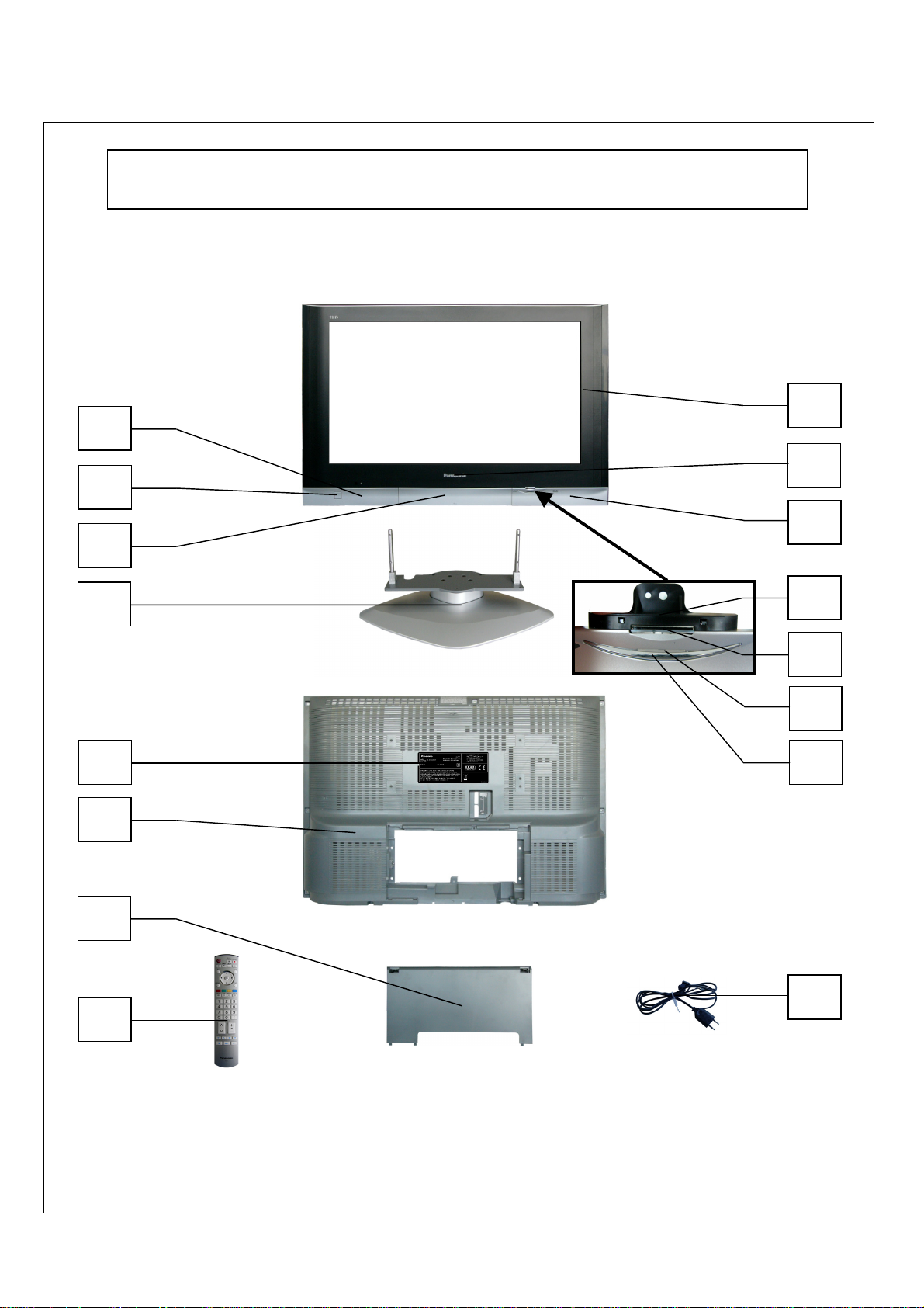
Parts Location
The numbers on the exploded view below refer to the exploded view section of the Replacement Parts List.
35
10
16
NOTE:
37
9
36
33
43
34
18
7
24
12
13
17
6
22

NOTE:
The numbers on the exploded view below refer to the exploded view section of the Replacement Parts List.
5
38
19
21
40
3
30
39
41
31
29
19
42
40
3
20
22
2
14
28
8
32
4
25
1
15
26
11
27
23
23
 Loading...