

Panasonic TX-32LMD70A, TX-32LMD70FA, TX-32LMD71FA, TX-32LMD72FA, TX-26LMD70A Service manual
...
ORDER No. PCZ0709109CE
Service Manual
Colour LCD Television
TX-32LMD70A
TX-32LMD70FA
TX-32LMD71FA
TX-32LMD72FA
TX-26LMD70A
TX-26LMD70FA
TX-26LMD71FA
GLP22M Chassis
Specifications
(Informations in brackets [ ] refers to model 26”)
Power Source: 220-240V AC, 50Hz
Power Consumption 135W [104W]
Stand-by Power Consumption: 1.0W (TV ONLY)
Aerial Impedance: 75Ω unbalanced, Coaxial Type
Receiving System: LMD70A LMD70FA
Receiving Channels: LMD70A LMD70FA
13W (TV+DVB set to record)
PAL-I PAL-I/H, B/G, D/K
PAL-525/60 (AV only) SECAM B/G, D/K, L/L’
DVB (via UHF aerial input) PAL-525/60 (AV only)
M.NTSC (AV only) DVB (via VHF/UHF aerial input)
NTSC (AV only) M.NTSC (AV only)
NTSC (AV only)
UHF E21-E68 VHF E2-E12 VHF H1-H2 (ITALY)
VHF A-H (ITALY) VHF R1-R2
VHF R3-R5 VHF R6-R12
UHF E21-E69 CATV (S01-S05)
CATV S1-S10 (M1-M10) CATV S11-S20 (U1-U10)
CATV S21-S41 (Hyperband)
Operating Conditions: Temperature: 0°C ÷ 35°C
Humidity: 20% ÷ 80% RH (non condensing)
Scanning format: 480i(60Hz), 480p(60Hz), 576i(50Hz), 576p(50Hz), 720p(60Hz), 720p(50Hz), 1.080i(60Hz),
1.080i(50Hz), 1.080p(60Hz), 1.080p(50Hz)
PC signals: VGA, SVGA, XGA, SXGA(compressed)
Horizontal scanning frequency 31 – 69 kHz
Vertical scanning frequency 59 – 86 Hz
Panasonic CS ( U.K. ) Ltd.
WILLOUGHBY ROAD,
BRACKNELL,
RG12 8FT.
BERKS.,

Intermediate Frequency:
Video/Audio LMD70A LMD70FA
Video 38,9MHz 38,9MHz, 33,9MHz
Audio 32.90MHz 33,4MHz (B/G), 33,16MHz (A2)
Colour 34,47MHz 34,47MHz (PAL)
Terminals:
AV1 IN Video (21 pin) 1V p-p 75Ω
AV1 OUT Video (21 pin) 1V p-p 75Ω
AV2 IN Video (21 pin) 1V p-p 75Ω
AV2 OUT Video (21 pin) 1V p-p 75Ω
AV3 IN S-Video IN (4-pin)Y: 1V p-p 75Ω
HDMI1, HDMI2 Type A Connector
COMPONENT Video (RCAx3) Y:1V p-p 75Ω (including synchronization)
AUDIO IN Audio (RCAx2) 500mV rms 10kΩ (for YUV; HDMI1)
AUDIO OUT Audio (RCAx2) 500mV rms 1kΩ (high Impedance)
32.35MHz(NICAM) 33,05MHz (NICAM B/G, D/K, L’)
32,4MHz (D/K), 32,66MHz (CZ STEREO)
40,4MHz (L’), 39,75MHz (L’ NICAM)
34,5MHz, 34,65MHz (SECAM)
38,3MHz, 38,15MHz (SECAM L’)
Audio (21 pin) 500mV rms 10kΩ
RGB (21 pin) 0,7V p-p 75Ω
Audio (21 pin) 500mV rms 1kΩ
Audio (21 pin) 500mV rms 10kΩ
RGB (21 pin) 0,7V p-p 75Ω
S-video IN (21-pin)Y: 1V p-p 75Ω
C:0,3V p-p 75Ω
Audio (21 pin) 500mV rms 1kΩ
C:0,286V p-p 75Ω
Audio (RCAx2) 500mV rms 10kΩ
Video (RCAx1) 1V p-p 75Ω
Pb, Pr: ±0,35V p-p 75Ω
PC HIGH-DENSITY D_SUB 15PIN R,G,B: 700mV p-p 75Ω
LCD screen: L5EDD8Q00037 [L5EDD6Q00026]
Audio Output: 20W (2x10W)
Headphones: 3,5mm (M3), 8Ω Impedance
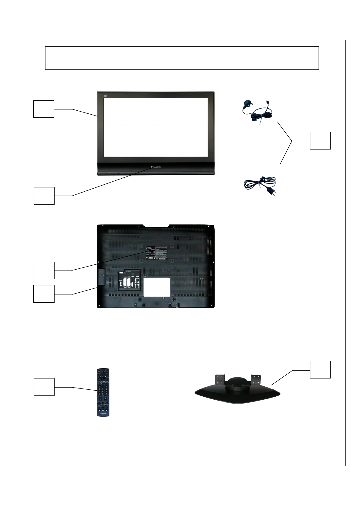
Accessories supplied : Remote Control 2 x R6 (UM3) Batteries
Dimensions:
Including TV stand 615mm 791mm 248mm
TV set only 563mm 791mm 117mm
Net weight: 17,5kg [14kg]
Specifications are subject to change without notice.
Weights and dimensions shown are approximate.
HD,VD:TTL Level 2-5V p-p (high impedance)
1366 x 768 XGA, 16:9
Visible Diagonal 800mm [660mm]
Height: Width: Depth:
[525mm] [657mm] [216mm]
[473mm] [657mm] [117mm]]
Warning
This service information is designed for experienced repair technicians only and is not designed for use by the general public. It does not
contain warnings or cautions to advise non-technical individuals of potencial dangers in attempting to service a product. Products
powered by electricity should be serviced or repaired only by experienced professional technicians. Any attempt to service or repair the
product or products deal within this service information by anyone else could result in serious injury or death.
2

CONTENTS
SAFETY PRECAUTIONS..........................................................................4
GENERAL GUIDE LINES..................................................................... 4
TOUCH – CURRENT CHECK.............................................................. 4
PREVENTION OF ELECTROSTATIC DISCHARGE (ESD)
TO ELECTROSTATICALLY SENSITIVE (ES) DEVICES..........................5
ABOUT LEAD FREE SOLDER (PBF)........................................................ 6
SUGGESTED PB FREE SOLDER....................................................... 6
APPLICABLE SIGNALS............................................................................. 7
SERVICE HINTS .......................................................................................8
CHASSIS BOARD LAYOUT...................................................................... 9
LOCATION OF LEAD WIRING…………………………………………….9
SETTING INSPECTION........................................................................... 10
SELF-CHECK .......................................................................................... 11
POWER LED BLINKING TIMING CHART...............................................12
SERVICE MODE FUNCTION..................................................................13
SERVICE ................................................................................................ 14
OPTION DESCRIPTION.......................................................................... 15
ADJUSTMENT METHOD ........................................................................ 16
WIRING DIAGRAM.................................................................................. 17
BLOCK DIAGRAMS................................................................................. 18
PARTS LOCATION.................................................................................. 21
REPLACEMENT PARTS LIST................................................................. 23
SCHEMATIC DIAGRAMS........................................................................ 43
P-BOARD (1 OF 2) SCHEMATIC DIAGRAM..................................... 44
DG-BOARD (1 OF 17) SCHEMATIC DIAGRAM................................ 46
G-BOARD SCHEMATIC DIAGRAM................................................... 63
V-BOARD SCHEMATIC DIAGRAM ................................................... 64
CONDUCTOR VIEWS............................................................................. 65
3
Safety Precautions
A
Ω
Ω
Ω
Ω
General Guide Lines
1. When servicing, observe the original lead dress. If a short circuit is found, replace all parts which have been overheated
or damaged by the short circuit.
2. After servicing, see to it that all the protective devices such as insulation barriers, insulation papers shields are properly
installed.
3. After servicing, make the following touch current checks to prevent the customer from being exposed to shock hazards.
4. Always ensure panel TKP0E16001 is correctly replaced before returning to customer (see Fig.1).
Fig. 1
Touch-Current Check
1. Plug the AC cord directly into the AC outlet. Do not use an isolation transformer for this check.
2. Connect a measuring network for touch currents between each exposed metallic part on the set and a good earth
ground such as a water pipe, as shown in Fig. 2.
3. Use Leakage Current Tester (Simpson 228 or equivalent) to measure the potential across the measuring network.
4. Check each exposed metallic part, and measure the voltage at each point.
5. Reserve the AC plug in the AC outlet and repeat each of the above measure.
6. The potential at any point (TOUCH CURRENT) expressed as voltage U1 and U2, does not exceed the following values:
For a. c.: U1 = 35 V (peak) and U2 = 0.35 V (peak);
For d. c.: U1 = 1.0 V,
Note:
The limit value of U2 = 0.35 V (peak) for a. c. and U1 = 1.0 V for d. c. correspond to the values 0.7 mA (peak) a. c. and
2.0 mA d. c.
The limit value U1 = 35 V (peak) for a. c. correspond to the value 70 mA (peak) a. c. for frequencies greater than 100
kHz.
7. In case a measurement is out of the limits specified, there is a possibility of a shock hazard, and the equipment should
be repaired and rechecked before it is returned to the customer.
Measuring network for TOUCH CURRENTS
COLD
WATER PIPE
(EARTH GROUND)
Fig. 2
CS=0.22μF
10k
U
1
0.022μF
V
U2 (V)
RS=1500
TO
PPLIANCES
EXPOSED
METAL PARTS
Resistance values in ohms (Ω)
V: Voltmetr or oscilloscope
(r.m.s. or peak reading)
NOTE – Appropriate measures should be taken to obtain the correct value in case of non-sinusoidal waveforms
Input resistance: ≥ 1M
Input capacitance: ≤ 200pF
Frequency range: 15Hz to 1MHz and d.c.respectively
R0=500
4

Prevention of Electrostatic Discharge (ESD) to Electrostatically
Sensitive (ES) Devices
Some semiconductor (solid state) devices can be damaged easily by static electricity. Such components commonly are
called Electrostatically Sensitive (ES) Devices. Examples of typical ES devices are integrated circuits and some field-effect
transistors and semiconductor "chip" components. The following techniques should be used to help reduce the incidence of
component damage caused by electrostatic discharge (ESD).
1. Immediately before handling any semiconductor component or semiconductor-equipped assembly, drain off any ESD on
your body by touching a known earth ground. Alternatively, obtain and wear a commerciall y av ailable discharging ESD
wrist strap, which should be removed for potential shock reasons prior to applying power to the unit under test.
2. After removing an electrical assembly equipped with ES devices, place the assembly on a conductive surface such as
aluminum foil, to prevent electrostatic charge build up or exposure of the assembly.
3. Use only a grounded-tip soldering iron to solder or unsolder ES devices.
4. Use only an anti-static solder removal device. Some solder removal devices not classified as "anti-static (ESD
protected)" can generate electrical charge sufficient to damage ES devices.
5. Do not use freon-propelled chemicals. These can generate electrical charges sufficient to damage ES devices.
6. Do not remove a replacement ES device from its protective package until immediately before you are ready to install it.
(Most replacement ES devices are packaged with leads electrically shorted together by conductive foam, aluminum foil
or comparable conductive material).
7. Immediately before removing the protective material from the leads of a replacement ES device, touch the protective
material to the chassis or circuit assembly into which the device will be installed.
Caution
Be sure no power is applied to the chassis or circuit, and observe all other safety precautions.
8. Minimize bodily motions when handling unpackaged replacement ES devices. (Otherwise harmless motion such as the
brushing together of your clothes fabric or the lifting of your foot from a carpeted floor can generate static electricity
(ESD) sufficient to damage an ES device).
IMPORTANT SAFETY NOTICE
There are special components used in this equipment which are important for safety.
These parts are marked by in schematic diagrams, exploded views and replacement parts list. It is essential that
these critical parts should be replaced with manufacturer’s specified parts to prevent shock, fire, or other hazards. Do
not modify the original design without permission of manufacturer.
5
About lead free solder (PbF)
Note: Lead is listed as (Pb) in the periodic table of elements.
In the information below, Pb will refer to Lead solder, and PbF will refer to Lead Free Solder.
The Lead Free Solder used in our manufacturing process and discussed below is (Sn+Ag+Cu).
That is Tin (Sn), Silver (Ag) and Copper (Cu) although other types are available.
This model uses Pb Free solder in it’s manufacture due to environmental conservation issues. For service and repair work,
we’d suggest the use of Pb free solder as well, although Pb solder may be used.
PCBs manufactured using lead free solder will have the PbF within a leaf Symbol
stamped on the back of PCB.
Caution
• Pb free solder has a higher melting point than standard solder. Typically the melting point is 50 ~ 70 °F (30~ 40°C)
higher. Please use a high temperature soldering iron and set it to 700 ± 20 °F (370 ± 10 °C).
• Pb free solder will tend to splash when heated too high (about 1100 °F or 600 °C).
If you must use Pb solder, please completely remove all of the Pb free solder on the pins or solder area before
applying Pb solder. If this is not practical, be sure to heat the Pb free solder until it melts, before applying Pb solder.
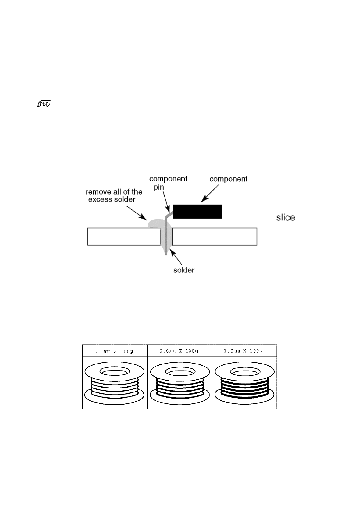
• After applying PbF solder to double layered boards, please check the component side for excess solder which may
flow onto the opposite side. (see Fig.3)
Fig.3
Suggested Pb free solder
There are several kinds of Pb free solder available for purchase. This product uses Sn+Ag+Cu (tin, silver, copper) solder.
However, Sn+Cu (tin, copper), Sn+Zn+Bi (tin, zinc, bismuth) solder can also be used. (see Fig.4)
Fig.4
6
Applicable signals
Component (Y, Pb, Pr), HDMI
Signal name COMPONENT HDMI
525 (480) / 60i * *
525 (480) / 60p * *
625 (576) / 50i * *
625 (576) / 50p * *
750 (720) / 60p * *
750 (720) / 50p * *
1,125 (1,080) / 60i * *
1,125 (1,080) / 50i * *
1,125 (1,080) / 60p *
1,125 (1,080) / 50p *
PC (D-sub 15P)
Signal name Horizontal frequency (kHz) Vertical frequency (Hz)
640 × 400 @70 Hz
640 × 480 @60 Hz
640 × 480 @75 Hz
800 × 600 @60 Hz
800 × 600 @75 Hz
800 × 600 @85 Hz
852 × 480 @60Hz
1,024 × 768 @60Hz
1,024 × 768 @70Hz
1,024 × 768 @75Hz
1,024 × 768 @85Hz
1,280 × 1,024 @60Hz
1,366 × 768 @60Hz
Macintosh 13“ (640 × 480)
Macintosh 16“ (832 × 624)
Macintosh 21“ (1,152 × 870)
Note:
• Signals other than above may not be displayed properly.
• The above signals are reformatted for optimal viewing on your display.
• Applicable input signal for PC is basically compatible to VESA standard timing.
• PC signal is magnified or compressed for display, so that it may not be possible to show fine detail
with sufficient clarity.
31.47 70.07
31.47 59.94
37.50 75.00
37.88 60.32
46.88 75.00
53.67 85.06
31.44 59.89
48.36 60.00
56.48 70.07
60.02 75.03
68.68 85.00
63.98 60.02
48.39 60.04
35.00 66.67
49.73 74.55
68.68 75.06
7
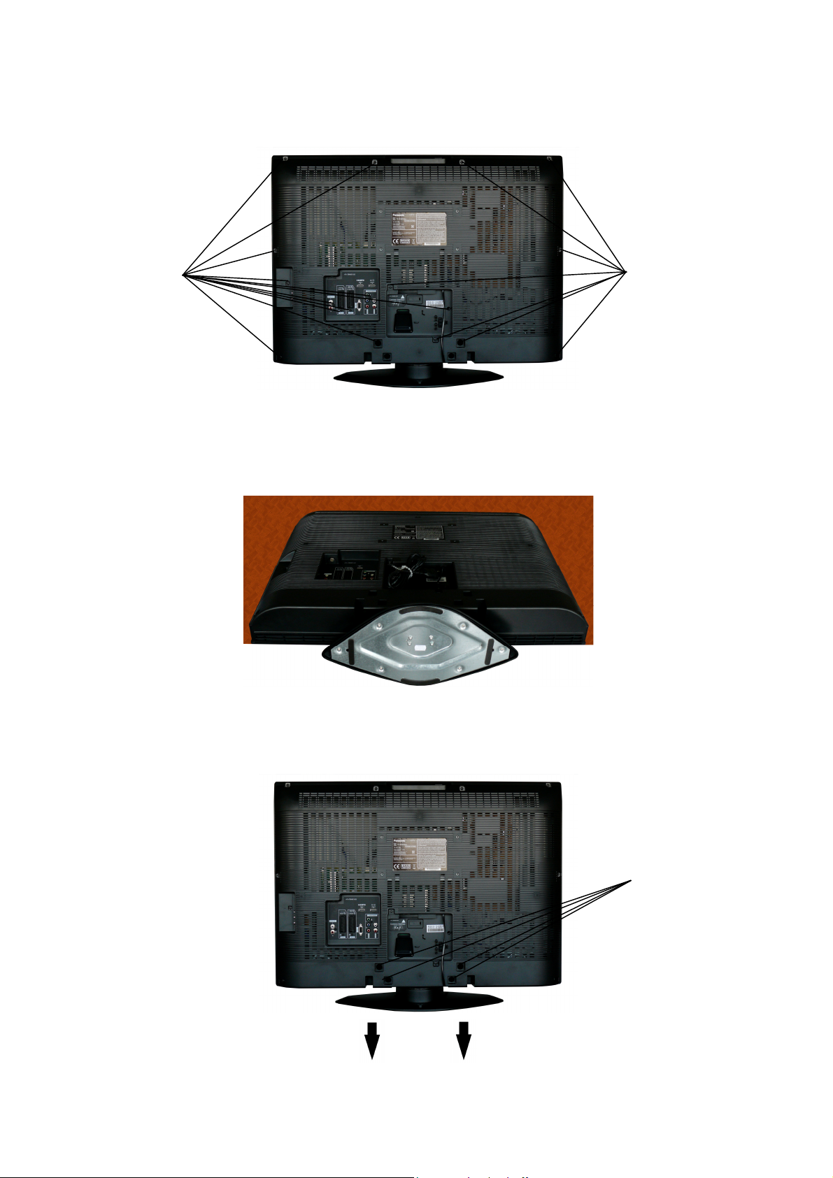
Service Hints
How to remove the backcover
Remove the 18[16] fixing screws. (see Fig.5)
SCREWS
How to remove the Pedestal assembly
Lay the main unit face down. (see Fig.6)
SCREWS
Fig.5
Fig.6
Remove the 4 fixing screws and the pedestal assembly. (see Fig.7)
Fig.7
SCREWS
8
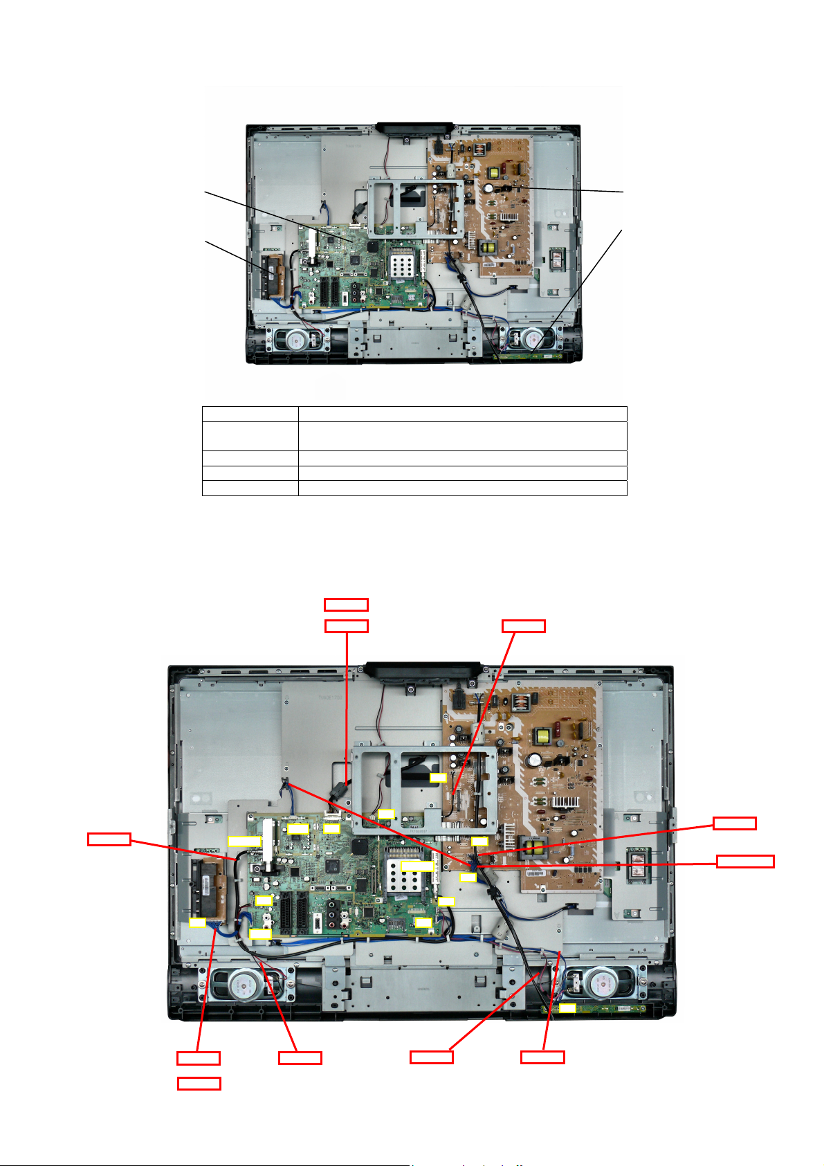
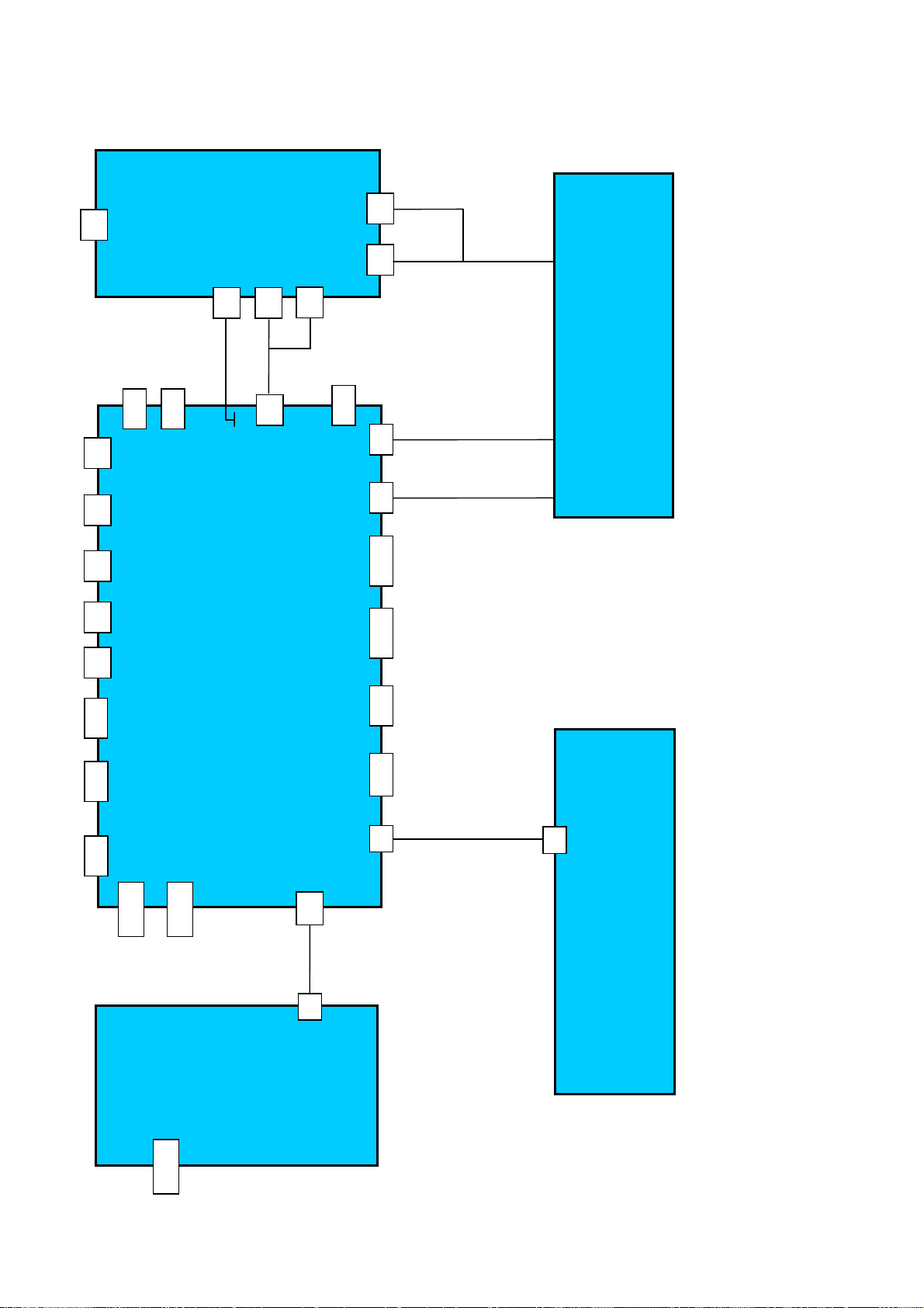
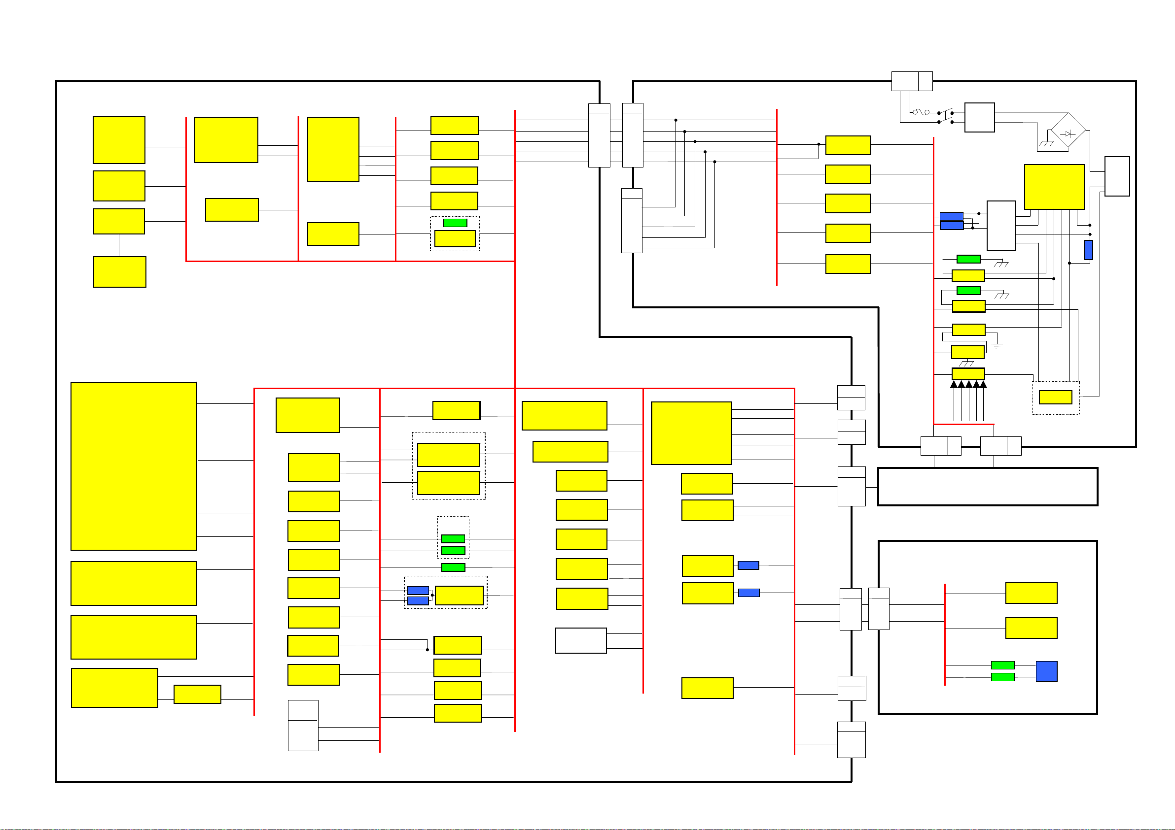
Chassis Board Layout
DG-BOARD
G-BOARD
Board Name Function
DG-Board Global Core, HDMI, IDTV Processor, D/A Converter,
AV Connector, Analog tuner, Digital tuner, AV Switch
G-Board Side AV Connector
P-Board Main Input, Power Supply, Main Switch
V-Board Remote Receiver, LED IR, Cats
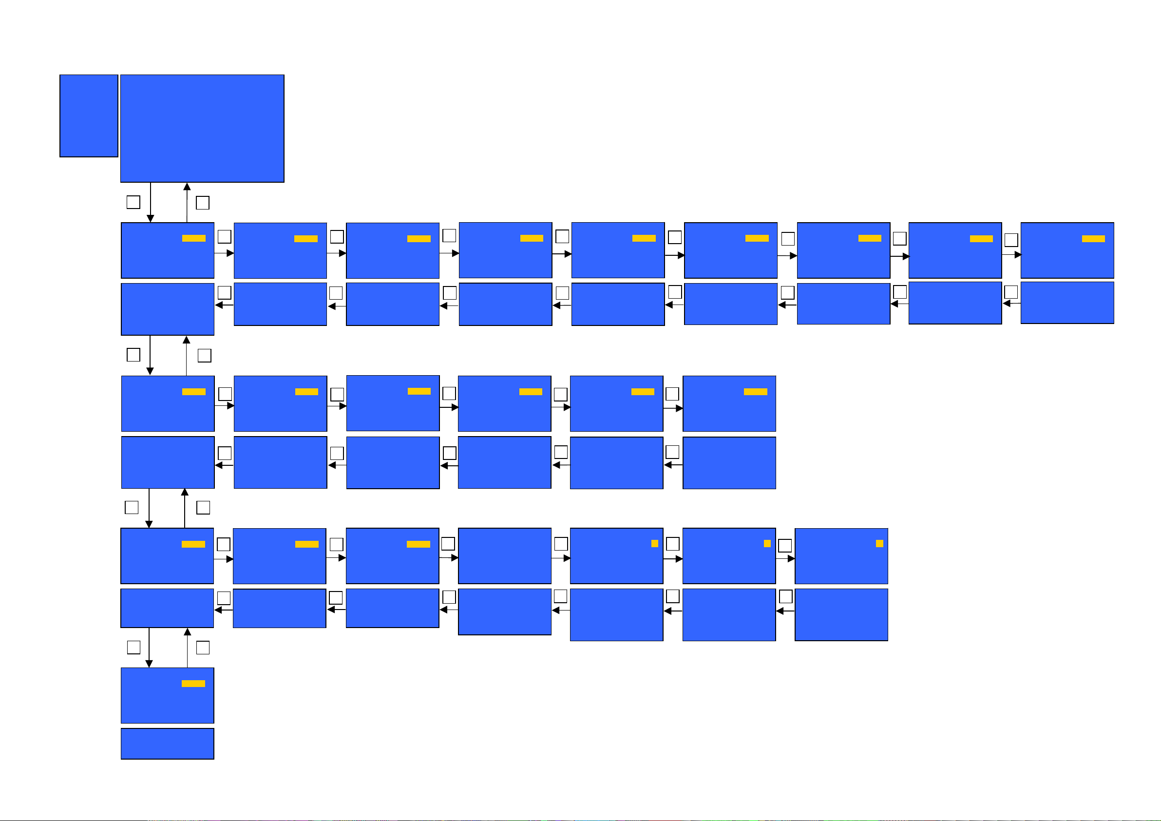
Location of Lead Wiring
To find the Part Number of required wire in Replacement Parts List click on the wire name in red box.
P-BOARD
V-BOARD
TNR-TN
G51
TU3200
DG8
DG51
DG11
( 26” )
( 32” )
DG5-PAN
DG5-PAN
DG5
DG9
TU8301
DG1
P7-DG
P7
P6-INV
P6
P2
DG7
( Only for 32” )
P2/DG11-INV
( 32” )
( 26” )
G51-DG51
G51-DG51
DG8-SP
V1
DG1-V1DG7-SP
9

Setting Inspection
Voltage Confirmation
Confirm the following voltages:
P board
Description Test point Position Normal mode Stand by mode Active stand by mode
Sub_5V TP861 P4, pin 12,13 5,0V +/- 0,25V
Panel 5/12V TP857 P4, pin 22,23 12V +/- 1V
15V_Audio TP856 C3861 15,5V +/- 1V
9V_Header TP864 P4, pin 7,6 9V +/- 0,25V
STBY_5V TP863 P4, pin 16 5,0V +/- 0,25V 5,0 +/- 0,25V 5,0V +/- 0,25V
24V_INV TP853 P2, pin1,2,3,4 24V +/- 1,5V
24V_INV TP852 C865 24V +/- 1,5V 24V +/- 1,5 24V +/- 1,5V
DG board
DTV9V TP5700 9V +/- 0,25V
SUB5V TP5701 5V +/- 0,25V
SUB3,3V TP5600 3,3V +/- 0,25V
MAIN9V TP5706 9V +/- 0,25V
STB5V TP5702 5V +/- 0,25V
SOUND15V TPS15 15V +/- 0,25V
<1V
<1V <1V
<1V <1V
<1V
<1V <1V
5,0V +/- 0,25V
9,0V +/- 0,25V
10
Self Check
A
A
A
f
A
A
A
A
A
A
f
A
A
A
Self-check is used to automatically check the bus lines and hexadecimal code of the TV set. To enter Self-Check mode, keep
pressing the down (-/v) button on the TV set and press the STATUS button on the remote control. To exit Self Check,
switch off the TV set at the power button.
TX-26LMD70FA
TX-26LMD71FA
TX-32LMD70FA
TX-32LMD71FA
TX-32LMD72FA
TX-26LMD70A
26
DV O.K.
VSW O.K.
DAV O.K.
SW O.K.
GENX O.K.
MEM1 O.K.
MEM2 O.K.
TUN1 O.K.
D-TUN O.K.
OFDM O.K.
32
DV O.K.
VSW O.K.
DAV O.K.
SW O.K.
GENX O.K.
MEM1 O.K.
MEM2 O.K.
TUN1 O.K.
D-TUN O.K.
OFDM O.K.
26
DV O.K.
VSW O.K.
DAV O.K.
SW O.K.
GENX O.K.
MEM1 O.K.
MEM2 O.K.
TUN1 O.K.
D-TUN O.K.
OFDM O.K.
Panasonic 2007LCD
Self Check Complete
PEAKS-SOFT 6.570
PEAKS-EEP 02.06.0035
GenX-SOFT 1.00.00
GenX-EEP 1.02.00
GenX-ROMCORR 1.01.00
Panasonic 2007LCD
Self Check Complete
PEAKS-SOFT 6.570
PEAKS-EEP 02.06.0034
GenX-SOFT 1.00.00
GenX-EEP 1.02.00
GenX-ROMCORR 1.01.00
Panasonic 2007LCD
Self Check Complete
PEAKS-SOFT
PEAKS-EEP
GenX-SOFT
GenX-EEP
GenX-ROMCORR
5.570
01.06.0039
1.00.00
1.02.00
1.01.00
26lmd70a.dat:000001
SUM
OPTION 1
OPTION 2
OPTION 3
CHECK
MODEL ID
32lmd70a.dat:000002
SUM
OPTION 1
OPTION 2
OPTION 3
CHECK
MODEL ID
26lmd70a.dat:000001
SUM
OPTION 1
OPTION 2
OPTION 3
CHECK
MODEL ID
18c3
ea
7f
95
04
189f
0c
ea
7f
75
04
03150000
00000002
189e
0c
ea
7
75
04
03150000
00000004
2c
03130000
00000002
Panasonic 2007LCD
Self Check Complete
5.570
01.06.0038
1.00.00
1.02.00
1.01.00
32lmd70a.dat:000002
SUM
OPTION 1
OPTION 2
OPTION 3
95
CHECK
04
MODEL ID
18c2
2c
ea
7
0313000
0000004
TX-32LMD70A
32
DV O.K.
VSW O.K.
DAV O.K.
SW O.K.
GENX O.K.
MEM1 O.K.
MEM2 O.K.
TUN1 O.K.
D-TUN O.K.
OFDM O.K.
PEAKS-SOFT
PEAKS-EEP
GenX-SOFT
GenX-EEP
GenX-ROMCORR
Display Ref. No. Description P.C.B.
ADV IC4510 A/D CONVERTER DG-Board
VSW IC3001 VIDEO SWITCH DG-Board
ADAV IC2106 AUDIO PROCESSOR DG-Board
ASW IC3101 AUDIO SWITCH DG-Board
TUN1 TU3200 ANALOG TUNER DG-Board
GENX IC1100 MICROPROCESSOR DG-Board
MEM1 IC1101 EEPROM DG-Board
MEM2 IC8601 EEPROM DG-Board
D-TUN TU8301 DIGITAL TUNER DG-Board
OFDM IC8301 COFDM DEMODULATOR DG-Board
If the CCU ports have been checked and found to be incorrect or not located then " - - " will appear in place of "O.K.".
11
Power LED blinking timing chart
1. Subject
Information of LED Flashing timing chart.
2. Contents
When abnormality has occurred the unit, the protection circuit operates and reset to the stand by mode. At this time, the
defective block can be identified by number of blinking of the Power LED on the front panel of the unit.
Blinking
times
Once
1 INVERTER_SOS
2 FAN_SOS DG BOARD
3SOS
4 DTV_9V DG BOARD
5 MAIN_9V DG BOARD
6 SUB_5V
7 MAIN_5V DG BOARD
Blinking timing Contents Check point
4 sec
Light
No Light
LCD PANEL
DG BOARD
DG BOARD
P BOARD
DG BOARD
V BOARD
8 MAIN_3.3V DG BOARD
9 SOUND_SOS DG BOARD
10 HQ1L_SOS DG BOARD
12

Service Mode Function
MPU controls the functions switching for each IICs through IIC bus in this chassis. The following setting and adjustment can be
adjusted by remote control in Service Menu
How to enter SERVICE
While pressing (-/v) button on TV unit, press on the remote
control for 3 times within 2 seconds.
Note:
To exit from Service mode, press the exit button on remote control.
0
13
SERVICE
Y
Y
A
A
A
A
A
Y
y
SERVICE
ADJUST
WB-ADJ
OPTION
SRV-TOOL
Peaks SOFT 6.570 OPTION 1 0c
Peaks EEP 02.06.0034 OPTION 2 ea
LSI DATA 0.00.02 OPTION 3 7f
GenX SOFT 1.00.00 Model ID 04
GenX EEP 1.02.00 03150000
GenX ROMCOR 1.01.00 00000004
HQ1L EEP -- Time 00000:00
Count 0000016
1
ADJUST DYNAMIC
CONTRAST
MAX
1,2:MAIN SELECT
3,4:SUB SELECT
9 :PICTURE MENU SELECT
ELLOW:AUTO ADJUST
VOL:ADJUST
OK :WRITE
1
000
2
ADJUST DYNAMIC
3
COLOR
1,2:MAIN SELECT
4
3,4:SUB SELECT
9 :PICTURE MENU SELECT
VOL:ADJUST
OK :WRITE
2
Key Command
• Press the 3/4 button to change the adjustment values or function.
• Press the 1/2 button to step up/down through the functions and adjustments
• Press the numerical button VOLUME (+/-) to change option item.
• Press the OK button after each adjustment has been made to store the required values.
DJUST DYNAMIC
3
3A
TINT
1,2:MAIN SELECT
4
3,4:SUB SELECT
9 :PICTURE MENU SELECT
VOL:ADJUST
OK :WRITE
00
ADJUST DYNAMIC
3
SUB-BRT
1,2:MAIN SELECT
4
3,4:SUB SELECT
9 :PICTURE MENU SELECT
VOL:ADJUST
OK :WRITE
808
DJUST DYNAMIC
3
BACKLIGHT
1,2:MAIN SELECT
4
3,4:SUB SELECT
9 :PICTURE MENU SELECT
VOL:ADJUST
OK :WRITE
276
DJUST DYNAMIC
H-POS
3
1,2:MAIN SELECT
4
3,4:SUB SELECT
9 :PICTURE MENU SELECT
VOL:ADJUST
OK :WRITE
DJUST DYNAMIC
0
H-AMP
3
1,2:MAIN SELECT
4
3,4:SUB SELECT
9 :PICTURE MENU SELECT
VOL:ADJUST
OK :WRITE
0
ADJUST DYNAMIC
V-POS
3
1,2:MAIN SELECT
4
3,4:SUB SELECT
9 :PICTURE MENU SELECT
VOL:ADJUST
OK :WRITE
DJUST DYNAMIC
0
V-AMP
3
1,2:MAIN SELECT
4
3,4:SUB SELECT
9 :PICTURE MENU SELECT
VOL:ADJUST
OK :WRITE
0
WB-ADJ DYNAMIC
R-GAIN
COLOR TEMP NORMAL
1,2:MAIN SELECT
3,4:SUB SELECT
7 :COLOR TEMP SELECT
9 :PICTURE MENU SELECT
VOL:ADJUST
OK :WRITE
1
OPTION DYNAMIC
Boot
1,2:MAIN SELECT
3,4:SUB SELECT
9 :PICTURE MENU SELECT
VOL:ADJUST
ROM
1
WB-ADJ DYNAMIC
FF
G-GAIN
3
COLOR TEMP NORMAL
1,2:MAIN SELECT
3,4:SUB SELECT
4
7 :COLOR TEMP SELECT
9 :PICTURE MENU SELECT
VOL:ADJUST
OK :WRITE
F2
WB-ADJ DYNAMIC
B-GAIN
3
COLOR TEMP NORMAL
1,2:MAIN SELECT
3,4:SUB SELECT
4
7 :COLOR TEMP SELECT
9 :PICTURE MENU SELECT
VOL:ADJUST
OK :WRITE
WB-ADJ DYNAMIC
E4
R-CENT
3
COLOR TEMP NORMAL
1,2:MAIN SELECT
3,4:SUB SELECT
4
7 :COLOR TEMP SELECT
9 :PICTURE MENU SELECT
VOL:ADJUST
OK :WRITE
48
WB-ADJ DYNAMIC
G-CENT
3
COLOR TEMP NORMAL
1,2:MAIN SELECT
3,4:SUB SELECT
7 :COLOR TEMP SELECT
9 :PICTURE MENU SELECT
VOL:ADJUST
OK :WRITE
WB-ADJ DYNAMIC
80
B-CENT
3
COLOR TEMP NORMAL
1,2:MAIN SELECT
3,4:SUB SELECT
44
7 :COLOR TEMP SELECT
9 :PICTURE MENU SELECT
VOL:ADJUST
OK :WRITE
40
2
OPTION DYNAMIC
STBY-SET
3
1,2:MAIN SELECT
4
3,4:SUB SELECT
9 :PICTURE MENU SELECT
OK :POWER OFF
OPTION DYNAMIC
00
Emergency
3
1,2:MAIN SELECT
4
3,4:SUB SELECT
9 :PICTURE MENU SELECT
VOL:ADJUST
OFF
OPTION DYNAMIC
/C Dela
3
1,2:MAIN SELECT
4
3,4:SUB SELECT
9 :PICTURE MENU SELECT
VOL:ADJUST
OK :WRITE
OPTION DYNAMIC
OPT 1
3
1,2:MAIN SELECT
4
3,4:SUB SELECT
5,6:BIT SELECT
9 :PICTURE MENU SELECT
VOL:ADJUST
OK :WRITE
00001100
OPTION DYNAMIC
OPT 2
3
1,2:MAIN SELECT
4
3,4:SUB SELECT
5,6:BIT SELECT
9 :PICTURE MENU SELECT
VOL:ADJUST
OK :WRITE
11101010
OPTION DYNAMIC
OPT 3
3
1,2:MAIN SELECT
4
3,4:SUB SELECT
5,6:BIT SELECT
9 :PICTURE MENU SELECT
VOL:ADJUST
OK :WRITE
01111111
2
SRV-TOOL DYNAMIC
1,2:MAIN SELECT
9 :PICTURE MENU SELECT
OK :ENTER
00
14
Option Bytes Description
OPTION1
0 ATP Speed Slow (1) / Fast (0)
1 TXT Ch On (1) / Off (0)
2 ID-1 On (1) / Off (0)
3 Macrovision Auto Evaluation On (1) / Off (0)
4 SRS Surround On (1) / Off (0)
5 Teletext Top Off (1) / On (0)
6 Not Use Not Use
7 Not Use Not Use
OPTION2
0 Not Use Not Use
1 A2 Stereo (5,5MHz) On (1) / Off (0)
2 A2 Stereo (6,0MHz) On (1) / Off (0)
3 A2 Stereo (6,5MHz) On (1) / Off (0)
4 Not Use Not Use
5 NICAM (5,5MHz) On (1) / Off (0)
6 NICAM (6,0MHz) On (1) / Off (0)
7 NICAM (6,5MHz) On (1) / Off (0)
OPTION3
0 NICAM priority (ASIA/M.E) On (1) / Off (0)
1 NICAM priority (K/UK) On (1) / Off (0)
2 NICAM priority (China) On (1) / Off (0)
3 NICAM priority (NZ/INDN) On (1) / Off (0)
4 NICAM priority (AUS) On (1) / Off (0)
5 NICAM priority (E.Europe) On (1) / Off (0)
6 NICAM priority (Special) On (1) / Off (0)
7 Not Use Not Use
15

Adjustment Method
Sub-Contrast/White Balance Adjustment
Instrument Name Connect to Remarks
1. Remote controller
2. LCD WB meter (Minolta CS-1000A equivalent)
3. Comunication jig
4. Computer for external control
Procedure Remarks
Subcontrast adjustment
1. Receive PAL colour bar (100% white) RF signal.
2. Enter “Contrast” adj. In SERVICE mode.
3. Start adjusting by using Yellow Key.
4. If the adjustment finished normally, the letter of Contrast will change from red
to black
Correlation can be also taken by
CA-210 or equivalent
Let the panel standfor more than 3
hours at more than 20 °C.
Basically perform adjustment in the
ambient environment of room
temperature more than 20 °C.
The aging time is more than20 min
at above room temperature.
Applied signal
100% full colour bar
0,7V p-p white peak
87.5% modulation
White Balance adjustment
1. Procedure basically performs checking using the production software and
make automatic adjustment using external computer.
2. It adjusts in the mode of : Colour balance Normal as follows.
Viewing Mode Dynamic
32LMD70A 32LMD70FA
WHITE Normal WHITE Normal
x: 0,2860 ± 0,010 x: 0,2860 ± 0,010
y:0,3090 ± 0,010 y:0,2960 ± 0,010
GRAY Normal GRAY Normal
x: 0,2860 ± 0,010 x: 0,2860 ± 0,010
y:0,3120 ± 0,010 y:0,3020 ± 0,010
26LMD70A 26LMD70FA
WHITE Normal WHITE Normal
x: 0,2860 ± 0,010 x: 0,2820 ± 0,010
y:0,3060 ± 0,010 y:0,2880 ± 0,010
GRAY Normal GRAY Normal
x: 0,2860 ± 0,010 x: 0,2820 ± 0,010
y:0,3090 ± 0,010 y:0,2880 ± 0,010
100% WHITE
50% GRAY
100% WHITE
50% GRAY
16
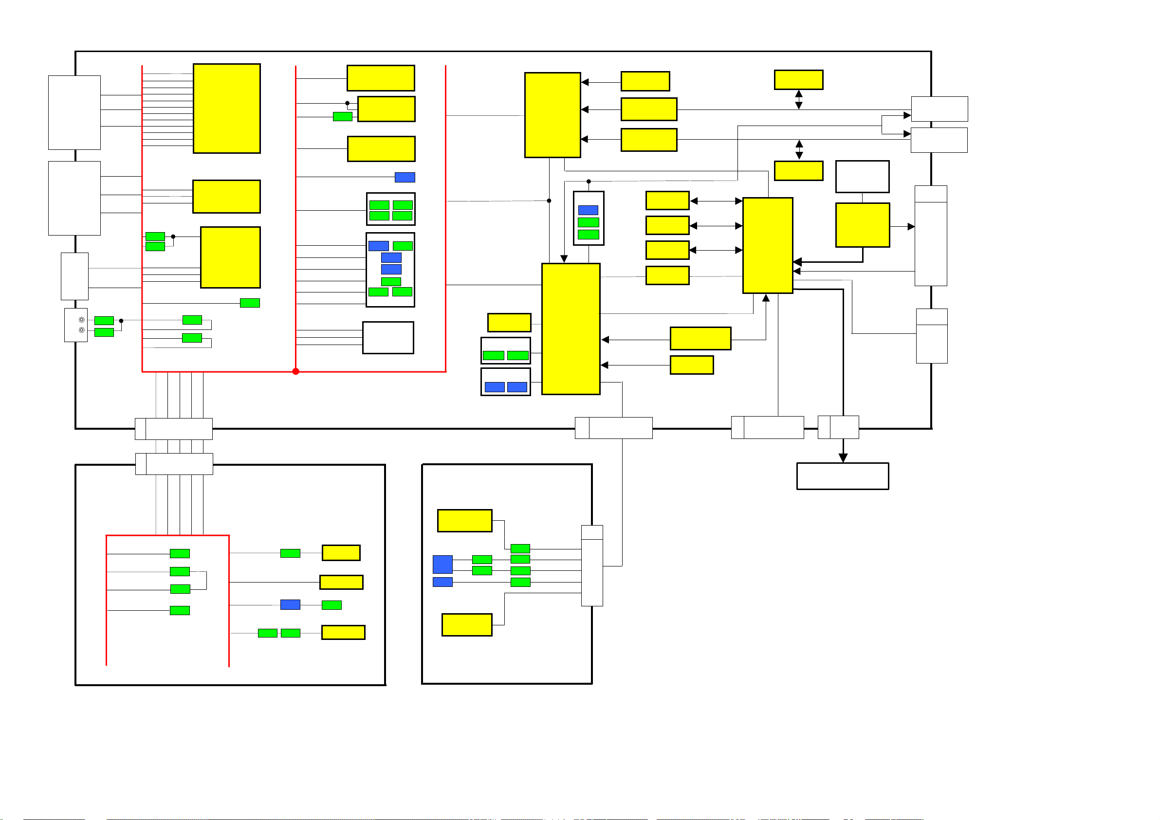
Wiring diagram
3003
17
P1
MAIN INPUT
P7
P-BOARD
P5
( 32” ONLY )
P6
P2
P4
SP_L
SP_R
SERVICE
SERVICE
KEY
HDMI 1 HDMI 2
DG7
DG8
DG32
DG33
DG9
JK4500
JK4501
CI SLOT
JK8401
PC INPUT
JK3001
DG-BOARD
SD SLOT
DG13
JK8801
DG5 DG11
AUDIO OUT
JK2002
AUDIO IN
JK3005
YPBPR
JK3004
DIGITAL
TUNER
TU8301
LCD PANEL
TUNER
TU3200
DG1
JK3002
AV1
K
AV2
DG51
G51
V1
V-BOARD
G-BOARD
JK3700
AV3
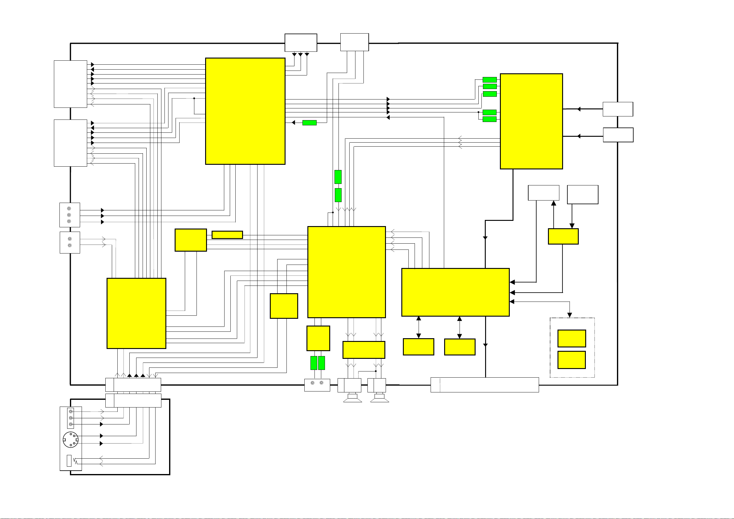
VIDEO & STEREO AUDIO BLOCK DIAGRAM
V
Y
X
V
A
,1P,2N,
,1P,2N,
18
JK3002
JK3003
YPBPR
AUDIO IN
AV1_V 20
AV1_VOUT 19
AV1_RED 15
AV1_GREEN 11
AV1_BLUE 7
AV1_L 6
AV1_LOUT 3
AV1_R 2
V1 21PIN SCART
AV1_ROUT 1
AV2_V 20
AV2_VOUT 19
AV2_C 15
AV2 GREEN 11
AV2 BLUE 7
AV2_L 6
AV2_LOUT 3
AV2_R 2
V2 21PIN SCART
AV2_ROUT 1
Y
PB
PR
JK3004
L
R
JK3005
DG-BOARD
(EXCHANGE UNIT)
YPBPR_Y
YPBPR_PB
YPBPR_PR
PC_LIN
PC_RIN
PC_LIN 10
PC_RIN 11
IC3101
AUDIO SWITCH
AV2_ROUT 26
AV2_R 15
AV2_LOUT 25
DTV_SL 39
DTV_SR 40
TUNER
TU3200
21
10
AM
VIDEO_OUT
11
SIF_OUT
Q4516
Q4515
Q4514
Q4519
Q4517
99 Y_IN
78 PB/C
94 PR
80 RGB_CVBS
97 SOY
8 HDMI_BCLK
3 HDMI_SDIN
7 HDMI_LRCK
16,17,18,24-33,
38-48,51-53,55,58
IC4510
ADV7493BBSTZ
112,113,115
,116,118,
119,121,122
128,129,131
,132,134,
135,137,138
RXA_CN,CP,ON,OP,
RXB_CN,CP,ON,OP,
2P
1N
2P
1N
JK4501
HDMI 1
JK4500
HDMI 2
1 AV1_V
33 AV1_VO
79 AV1_RED
77 AV1_GREEN
81 AV1_BLUE
8,10 AV2_V
31 AV2_VO
12 AV2_C
53 AV2_RED/C
51 AV2_GREEN
55 AV2_BLUE
63 YPBPR_Y
IC3001
VIDEO SWITCH
(AN15876A)
MAIN_PB_OUT 39
MAIN_PR_OUT
MAIN_RGB_CVBS_OUT 44
MAIN_RF_CVBS
65 YPBPR_PB
67 YPBPR_PR
95 AV4_
PC_R 75
PC_G 71
PC_B
MAIN_Y_OUT 40
DVB_CVBS 20
97 AV4_
99 AV4_C
73
38
91
PC INPUT
JK3001
3
1
2
Q3200
Q2017
JK8401
DATA
CI SLOT
SERIAL
BUS
IC8301
DEMODULATOR
TS
Q2016
IC2002
AUDIO
DAC
11
1
IC2006
2
3
10
4
24
34
OUT
35 BCLK
37 SDTI
36 LRCK
58 HPOUTR1
57 HPOUTL1
8
AINR2 77
SIF_IN1
AINL2 76
74 AUXOUTL2
75 AUXOUTR2
79 AV_R
78 AV_L
AV2_L 14
AV1_L 16
AV1_R 17
AV1_LOUT 23
AV1_ROUT 24
5
3
IC2012
HP
AMPLIFIER
1
7
72 AUXOUTL1
73 AUXOUTR1
DTV_BCLK 19
DTV_LRCK 18
DTV2_SDIN 23
HDMI_SDIN 22
HDMI_LRCK 26
HDMI_BCLK 27
IC2106
AUDIO
PROCESSOR
43 SQ_L-
42 SQ_L+
DTV_SDIN 24
45 SQ_R-
44 SQ_R+
B13
A13F14D15
IC8001-PeaksLite2
DVB_CVBS
D12
MN2WS0039A
VIDEO / AUDIO IF
I1P2-VI1P9,VI1P12-
I1P19,VI1P22-VI1P29
CLK,CLKOA,VSYNC,HS
2-A9,B1,B3-B10,C1,C2,
C4-C10,D1,D2,E2,E3
B25,B26,C25,C26,D25,D26
,E25,E26,F25,F26,G25,G26
NC,ENB
TU8301
DIGITAL
TUNER
COFDM
R
L
JK3700
TV_L 41
TV_R 42
AV_R 33
5
7
571
G-BOARD
AV_L 32
3
1
3
6 AV4_L
7 AV4_R
11
13
15
13
11
15
AV4_R
AV4_L
AV4_V
AV4_Y
Y
AV4_C
C
L
HP_LOUT
HP_ROUT
G51 DG51
R
HP_LOUT
HP_ROUT
761
IC2011
AUDIO
AMPLIFIER
2
Q2015
L
JK2002
AUDIO OUT
IC8002
16
18
AUDIO AMPLIFIER
43
36
Q2021
R
DG8
1
2
IC2301
3
8
31
DG7
6
IC8601
EEPROM
IC8554
16 MB FLASH
24
TE1P,TE1N,TD1P,TD1N,TCLK
1P,TCLK1N,
TC1P,TC1N,TB1P,TB1N,TA1P,
TA1N
1
3
DG5
1-15
DDR2-0
IC8003
DDR2-1
TO LCD PANEL
SP_R
SP_L
POWER SUPPLY BLOCK DIAGRAM
V
V
V
V
A
A
V
V
V
6
V
V
V
19
DG-BOARD
(EXCHANGE UNIT)
IC3001
IDEO
SWITCH
6, 25,
45, 69
IC3101
AUDIO
SWITCH
IC2013
REG
5
5V
8
IC2012
HP AMPLIFIER
DTV9V
DTV9V
5
MAIN9V
4
IC2301
AUDIO
AMPLIFIER
26, 27, 32, 35, 40, 41
1, 21, 22, 23, 44
IC2002
AUDIO DAC
7,8,
9,14
SOUND15V
SOUND12V
SUB5
PROCESSOR
4, 53, 59, 68, 71
14, 21, 31, 40, 51
IC2011
AMPLIFIER
IC2106
AUDIO
12
29
8
3,3V
AUD3,3V
SUB3,3V
DVDD1,8V
DTV9V
3,3V
AUD3,3V
DVDD1,8V
SOUND12V
BT30V
IC2010
5Vout
IC2008
1Vout
IC2107
1Vout
IC2303
1Vout
Q2639
IC2610
REGULATOR
REG
REG
REG
REG
Vin1
Vin7
Vin7
Vin3
SUB5V
SUB5V
SUB3,3V
SOUND15V
DTV9V
SOUND_15V
DTV9V
SUB_5V
5V_STBY
P12V
DG13
1-2
6-7
12-13
16
22-23
P4
1-2
6-7
12-13
16
22-23
1-2
6-7
12-13
16
22-23
P-BOARD
SOUND_15V
9V_HEADER
SUB_5V
5V_STBY
PANEL_5V/12V
15V_AUDIO
SOUND_15V
PANEL_5V/12V
SUB_5V
9V_HEADER
5V_STBY
IC3850
2
IC3851
2
IC3852
2
IC3853
2
IC3854
1
REG
REG
REG
REG
REG
1
1
1
1
3
24V_IN
24V_IN
24V_IN
24V_IN
24V_IN
MAIN IN
21
F801
P1
24V_IN
SW 801
D854
D851
LF804
FILTER
Q851
PC801
Q852
PC802
LINE
T801
7
14
3
4
6
2
D801
-
IC802
MAIN PS CONTROL
11
15
10
19
20
~
+
~
T802
2
4
7
23
7
D818
P16, H21, P3, E22, E23, F21, C12, E14,
AA8, AA9, A25, A26, B24, C23, D7, D8,
D16, D17, D22, E21, F11, F12, F15, F20,
G4, H4, J6, K6, N6, P6, R4, T4, U6,
M17, U15, T17, N17, R17, T15, U16,
AB15, AC15, AD 15, AE1 5, AF15 , U14,
N10, P10, R10, R11, R12, R13, T10,
T11, T12, T13, U10, U11, U12, U13,
AA14, AB14, AC14, AD14, AE14, AF14
IC8001-PeaksLite
PROCESSOR
K23, K26, M21, M23, N24, P25, R21,
T25, U24, V22, W26, Y22, Y24, AA21,
AB19, AB22, AB 25, AC1 8, AC23 , AD17,
AD22, AD25, AE16, AE21, AF20, AF26
A1, E1, M9, J9, R1, J1, A9, C1, C3, C7,
A1, E1, M9, J9, R1, A9, C1, C3, C7, C9,
2, 13, 15, 16, 17, 18, 33, 45, 54
IC8301
LVDS DRIVER
C9, E9, G1, G3, G7, G9
IC8002
MEMORY
IC8003
MEMORY
7, 19, 21, 28
AC10, AC11
1, 21, 22, 23, 44
E9, G1, G3, G7, G9, J1
1,8V
1Vout
IC8302
REG
SUB3,3V
SUB1,2
SUB1,8V
SOUND12V
1,8V_DDRI/F
1,8V_DDRI/F
SUB3,3V
SUB3,3V
Vin8
IC8004
CLOCK
GENERATOR
5, 13, 15
IC8401
DATA BUFFER
IC8402
TS BUFFER
IC8404
TS BUFFER
IC8405
TS BUFFER
IC8406
TS BUFFER
IC8407
TS BUFFER
IC8408
TS BUFFER
IC8409
TS BUFFER
JK8401
CI SLOT
17, 18
51, 52
23,24
PC803
IC 851
PC804
PC1001
RM1001
REMOTE
D1001
IC801
STB3,3V
MAIN3,3V
P12V
STB3,3
SUB5V
STB5V
SUB5V
DVDDIO3,3V
D4525
D4527
VDD3,3V
TVDD3,3V
DVDD1,8V
CVDD1,8V
MAIN3,3V
SUB5V
MAIN5V
MAIN5V
MAIN5
SUB3,3V
SUB5V
SUB3,3V
SUB1,8V
SUB1,2V
SUB5V
1
SUB3,3V
20
20
20
20
20
SUB3,3V
20
SUB3,3
20
5VCARD
5VCARD
SUB5V
SUB5V
SUB5V
SUB5V
SUB5V
SUB3,3V
SUB5V
SUB3,3V
DTV9V
SUB5V
STB5V
TVDD3,3V
AVDD3,3V
DVDDIO3,3V
CVDD1,8
DVDD1,8V
D5671
D5673
IC8403
REG
1Vin
Peaks-LITE2 POWER
3Vout
IC5601
REG
12Vout
IC5600
23Vout
REG
MAIN5V/
MAIN3,3V
Q5692
Q5693
Q5561
GenX4 POWER
IC5670
1Vin
REG
IC4506
REG
1Vout
IC4507
REG
5Vout
IC4508
REG
1Vout
IC4509
REG
1
Vout
Vout6
Vin
Vin
23
17
Vout5
Vin7
Vin1
Vin8
Vin8
5VCARD
DTV9V
DTV9V
MAIN5V
MAIN3,3V
MAIN9V
STB3,3V
SUB5V
SUB5V
SUB3,3V
SUB3,3V
IC1100
MICROPROCESSOR
31, 50, 74, 78, 81, 85, 94, 108
IC8554
NOR FLASH
IC8621
DeMPX
IC8622
DeMPX
IC1101
EAROM
IC5671
RESET IC
IC5660
RESET IC
TU3200
29, 43, 53
5,9,16
20
20
18
8
2
1
2
1
STB3,3V
SUB3,3V
SUB3,3V
SUB3,3V
STB3,3V
STB5V
STB3,3V
DTV9
SUB3,3,
SUB5V
BT30V
IC4510
DV7493BBSTZ
68, 71, 101, 104, 109,
84, 88
111, 123, 127,
23, 57, 142
125, 141
15, 35, 50, 67
IC4504
EEPROM
IC4515
COMPARATOR
IC4500
EDID EPROM
IC4501
EDID EPROM
IC8601
EEPROM
139
8,3
8
5
8
8
8
4
1
27, 29
30, 31
DG1
4
1
3, 11
V-BOARD
4
22
1-4
STB3.3V
SUB5V
5V_STBY
PAN_5V/12
9V_HEADER
15V_AUDIO
24V_IN
P2
LCD PANEL
SUB5V
STB3,3V
STB3.3V
STB3.3V
SUB_5
24V_IN
1-4
P
Q1004
Q1002
CONTROL BLOCK DIAGRAM
V
20
JK3002
JK3003
PC AUDIO IN
AV1_SLOW 8
AV1_QLINK 10
AV1_FB 16
V1 21PIN SCART
AV2_SLOW 8
AV2_QLINK 10
AV2_FB 16
V2 21PIN SCART
13
14
JK3001
R
JK2002
L
AUDIO OUT
PC_H_IN
PC_V_IN
MONITOROUT_MUTE
Q2002
Q2003
AV2_SLOW
PC_V
PC_H
FB
AV2_FB
AV1_FB
PC_V_IN
PC_H_IN
AV1_SLOW
SDA0B_5V
SCL0B_5V
VIDEO_STATUS
DAC_PD
SCL0B_5V
SDA0B_5V
AUDIO_MUTE
Q2102
Q2101
SOUND_SOS
SDA2
SCL2
AUDIO_XRST
TV_SUB_ON_DELAY
SDA0B_5V
SD2
SCL0B_5V
SCL2
MUTE
Q2641
Q2640
4
41
42
46,74
48
49
IC3001
58
VIDEO SWITCH
60
80
83
84
85
22
IC3101
35
AUDIO SWITCH
36
15
PROCESSOR
16
17
50
IC2106
AUDIO
Q2635
DAC_PD
AMUTE
SOUND_SOS
AMUTE
SOS
MONITOROUT_MUTE
AUDIO_MUTE
SP_MUTE
HDMI_INT2
MONITOROUT_MUTE
AMUTE
24V_DET
SCL0B_5V
SDA0B_5V
RF_AFT1
Q2301
5
7
17
5
2
IC2002
AUDIO DAC
IC2301
AUDIO AMP
IC2012
HP AMP
AV1-2 OUT MUTE
Q2005
Q2004
Q2007
Q2006
MUTE SW
Q2034
D2028
D2031
D2032
Q2031
Q2039
Q2040
13
14
TUNER
20
D2637
DATA CONTROL
DATA CONTROL
DATA CONTROL
IC5660
RESET IC
MAIN5
MAIN3.3V
Q5691 Q5690
QLINK
D1102D1100
IC4510
ADV7493B
IC1100
MICROPROCESSOR
HDMI CEC
Q1107
Q1108
IC4504
EEPROM
IC4513
LEVEL
TRANSLATING
IC4514
LEVEL
TRANSLATING
IC8002
IC8003
IC8554
IC8004
CLK GEN
DDR2
DDR2
FLASH
IC8601
EEPROM
IC1101
EEPROM
IC8001
PeaksLite2
IC4501
EEPROM
IC4500
EEPROM
SERIAL bus
LVDS bus
DG - BOARD
(EXCHANGE UNIT)
HDMI CEC
TU8301
DIG TUNER
IC8301
COFDM DEM
HDMI1
JK4501
HDMI2
JK4500
JK8401
CI SLOT
DATA
JK8801
SD CARD
Q2003
P - BOARD
PANEL_12V_ON
TUNER_SUB_ON
SUB_ON
TUNER_MAIN_ON
PANEL_12V_ON
DG13
P4
PANEL_12V_ON
19
19
TV_SUB_ON
18
18
TUNER_SUB_ON
Q3863
Q3870
Q3871
Q3855
TV_MAIN_ON
TUNER_MAIN_ON
DG1
V1
5
8
7
6
1
REMOTE
DG33
SERVICE
DG5
LCD PANEL
24V_DET
SOS
5
17
15
5
17
15
V - BOARD
RM1001
24V_DET
SOS
SUB_ON
24V_DET
SOS
SUB_ON
Q851
D3860
Q3867 Q3867
PC801
1
IC3855
Q3865
5
IC1101
REMOTE
PC1001
CATS
OUT
Q1004
Q1002
Q1010
Q1006
Q1007
Q1009
4
REMOTE
G_LED_ON
R_LED_ON
TIMER_REC_LED
AI_SENSOR
Parts Location
The numbers on the exploded view below refer to the exploded view section of the Replacement Parts List.
17
5
NOTE:
(UK)
15
(CONTINENTAL)
27
16
3
28
21
 Loading...