

Panasonic TX-20LB5FG, SL-120PPP Schematic
ORDER NO. PCZ0602001CE
Service Manual
LCD TV
TX-20LB5F/G
TX-20LB5P/G
SL-120PP Chassis
Power Source
AC 100-240V, 50/60Hz TV set DC 15V, 4.67A Max.
Power Consumption
Average use: 50W
Standby condition: 2.5W
LCD
VGA (640 × 480 pixels)
4:3 aspect ratio LCD panel
Screen Size
408 mm(W) × 306 mm(H)
Sound
Speaker
9 cm × 5cm, 2pcs, 4Ω
Audio Output
4W (2W + 2W), 20% THD
Headphones
M3 (3.5 mm) Jack x 1
Receiving Systems/ Band name
VHF BAND I: CH2-CH4
BAND II: CH5-CH12
UHF HYPER BAND :SI’-S3’, S1-S20
BAND IV, V : CH21-CH68
PAL-B/G, D/K, SECAM-L/L’, NTSC(AV input only)
Aerial-Rear
UHF/VHF
Operating Conditions
Temperature: -10°C ~ 40°C
Humidity: 0% ~ 90% RH (non-condensing)
Connection Terminals
AV1 (Scart connecter)
21 Pin terminal (Audio/Video in, Audio/Video out,
RGB in)
AV2
VIDEO
RCA PIN Type × 1
S-VIDEO
Mini DIN 4-pin
AUDIO L-R
RCA PIN Type × 2
Dimensions (W x H x D)
Including TV Stand
608mm(W) × 215mm(D) × 457.5mm(H)
TV Set Only
608mm(W) × 73,7mm(D) × 403mm(H)
Weight
10.1kg Net
Note:
Design and Specifications are subject to change without
notice.
Weight and Dimensions shown are approximate.
© 2006 Matsushita Electric Industrial Co., Ltd.
All rights reserved. Unauthorized copying and
distribution is a violation of law.

TX-20LB5F/G
TX-20LB5P/G
CONTENTS
Page
1. Safety Precautions ----------------------------------------------- 3
1.1. General Guidelines -------------------------------------- 3
1.2. Touch-Current Check ------------------------------------ 3
2. Prevention of Electro Static Discharge (ESD) to
Electrostatically Sensitive (ES) Devices ------------------ 4
3 About lead free solder (PbF) --------------------------------- 5
4. Self Check ---------------------------------------------------------- 6
5. Chasis Board Layout -------------------------------------------- 7
6. Before servicing -------------------------------------------------- 8
6.1. Wire dressing ---------------------------------------------- 8
7. Disassembly for service --------------------------------------- 9
7.1. Stand ass´y ------------------------------------------------ 9
7.2. Back cover ------------------------------------------------- 9
7.3. CTRL ass´y -----------------------------------------------10
7.4. LED ass´y -------------------------------------------------10
7.5. AV ass´y ----------------------------------------------------11
7.6. INVERTER ------------------------------------------------11
7.7. TTL ass´y -------------------------------------------------- 11
7.8. Speaker (left and right) --------------------------------- 11
7.9. Main ass´y -------------------------------------------------12
7.10.Panel LCD -------------------------------------------------12
Page
8 Service Mode Function ----------------------------------------13
8.1. How to enter SERVICE 1 ------------------------------13
8.2. How to enter SERVICE 2 ------------------------------13
8.3. Option Description --------------------------------------14
9. Conduct Views ---------------------------------------------------16
9.1. Foil Side ---------------------------------------------------16
9.2. Component Side -----------------------------------------18
10. Block and Schematic Diagrams --------------------------20
10.1. Schematic Diagram Notes ---------------------------20
10.2. Block Diagram ------------------------------------------21
10.3. Schematic Diagram -----------------------------------22
11. Parts Location & Replacement Parts List -------------28
11.1. Different parts List -------------------------------------28
11.2. Exploded View ------------------------------------------29
11.3. Stand Assy Exploded View --------------------------30
11.4. Packing Exploded Views -----------------------------31
11.5. Electrical Replacement Parts List ------------------32
2
TX-20LB5F/G
TX-20LB5P/G
1 Safety Precautions
1.1. General Guidelines
1. When servicing, observe the original lead dress. If a short circuit is found, replace all parts which have been overheated or
damaged by the short circuit.
2. After servicing, see to it that all the protective devices such as insulation barriers, insulation papers shields are properly
installed.
3. After servicing, make the following leakage current checks to prevent the customer from being exposed to shock hazards.
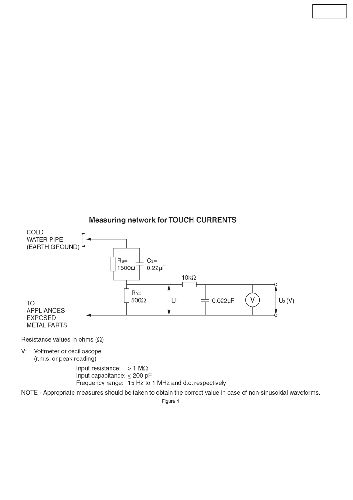
1.2. Touch-Current Check
1. Plug the AC cord directly into the AC outlet. Do not use an isolation transformer for this check.
2. Connect a measuring network for touch currents between each exposed metallic part on the set and a good earth ground such
as a water pipe, as shown in Figure 1.
3. Use Leakage Current Tester (Simpson 228 or equivalent) to measure the potential across the measuring network.
4. Check each exposed metallic part, and measure the voltage at each point.
5. Reserve the AC plug in the AC outlet and repeat each of the above measure.
6. The potential at any point (TOUGH CURRENT) expressed as voltage U1 and U2, does not exceed the following values:
For a. c.: U
For d. c.: U
Note:
The limit value of U2 = 0.35 V (peak) for a. c. and U1 = 1.0 V for d. c. correspond to the values 0.7 mA (peak) a. c. and 2.0
7. In case a measurement is out of the limits specified, there is a possibility of a shock hazard, and the equipment should be
repaired and rechecked before it is returned to the customer.
1 = 35 V (peak) and U2 = 0.35 V (peak);
1 = 1.0 V,
mA d. c.
The limit value U1 = 35 V (peak) for a. c. correspond to the value 70 mA (peak) a. c. for frequencies greater than 100 kHz.
3
TX-20LB5F/G
TX-20LB5P/G
2 Prevention of Electro Static Discharge (ESD) to
Electrostatically Sensitive (ES) Devices
Some semiconductor (solid state) devices can be damaged easily by static electricity. Such components commonly are called
Electrostatically Sensitive (ES) Devices. Examples of typical ES devices are integrated circuits and some field-effect transistors and
semiconductor „chip” components. The following techniques should be used to help reduce the incidence of component damage
caused by electro static discharge (ESD).
1. Immediately before handling any semiconductor component or semiconductor-equipped assembly, drain off any ESD on your
body by touching a known earth ground. Alternatively, obtain and wear a commercially available discharging ESD wrist strap,
which should be removed for potential shock reasons prior to applying power to the unit under test.
2. After removing an electrical assembly equipped with ES devices, place the assembly on a conductive surface such as almi-
num foil, to prevent electrostatic charge buildup or exposure of the assembly.
3. Use only a grounded-tip soldering iron to solder or unsolder ES devices.
4. Use only an anti-static solder removal device. Some solder removal devices not classified as „anti-static (ESD protected)” can
generate electrical charge sufficient to damage ES devices.
5. Do not use freon-propelled chemicals. These can generate electrical charges sufficient to damage ES devices.
6. Do not remove a replacement ES device from its protective package until immediately before you are ready to install it. (Most
replacement ES devices are packaged with leads electrically shorted together by conductive foam, alminum foil or comparable
conductive material).
7. Immediately before removing the protective material from the leads of a replacement ES device, touch the protective material
to the chassis or circuit assembly into which the device will be installed.
Caution
Be sure no power is applied to the chassis or circuit, and observe all other safety precautions.
8. Minimize bodily motions when handling unpackaged replacement ES devices. (Otherwise hamless motion such as the brush-
ing together of your clothes fabric or the lifting of your foot from a carpeted floor can generate static electricity (ESD) sufficient
to damage an ES device).
4

TX-20LB5F/G
TX-20LB5P/G
3 About lead free solder (PbF)
Note: Lead is listed as (Pb) in the periodic table of elements.
In the information below, Pb will refer to Lead solder, and PbF will refer to Lead Free Solder.
The Lead Free Solder used in our manufacturing process and discussed below is (Sn+Ag+Cu).
That is Tin (Sn), Silver (Ag) and Copper (Cu) although other types are available.
This model uses Pb Free solder in it’s manufacture due to environmental conservation issues. For service and repair work, we’d
suggest the use of Pb free solder as well, although Pb solder may be used.
PCBs manufactured using lead free solder will have the PbF within a leaf Symbol
Caution
• Pb free solder has a higher melting point than standard solder. Typically the melting point is 50 ~ 70 °F (30~40°C) higher.
Please use a high temperature soldering iron and set it to 700 ± 20 °F (370 ± 10 °C).
• Pb free solder will tend to splash when heated too high (about 1100 °F or 600 °C).
If you must use Pb solder, please completely remove all of the Pb free solder on the pins or solder area before applying Pb
solder. If this is not practical, be sure to heat the Pb free solder until it melts, before applying Pb solder.
• After applying PbF solder to double layered boards, please check the component side for excess solder which may flow onto
the opposite side. (see figure below)
Suggested Pb free solder
There are several kinds of Pb free solder available for purchase. This product uses Sn+Ag+Cu (tin, silver, copper) solder.
However, Sn+Cu (tin, copper), Sn+Zn+Bi (tin, zinc, bismuth) solder can also be used.
stamped on the back of PCB.
5
TX-20LB5F/G
TX-20LB5P/G
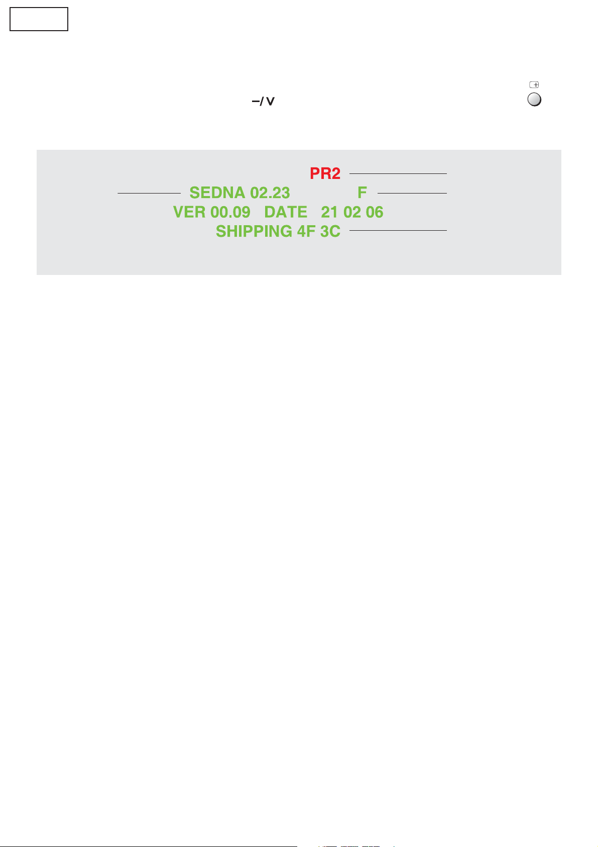
4 Self Check
1. Self-Check is used to automatically check the bus lines and hexadecimal code of the TV set.
2. To get into the Self -Check mode press the Down (
button on the remote control, and the screen will show when the self Check is finished:
SEDNA VERSION
3. Turn off the TV to reset after SELF-CHECK menu.
) button on the TV set, at the same time pressing the Recall ( )
Programm number
Software Type
When Self Check is
finished you have this line
within the option definition.
6
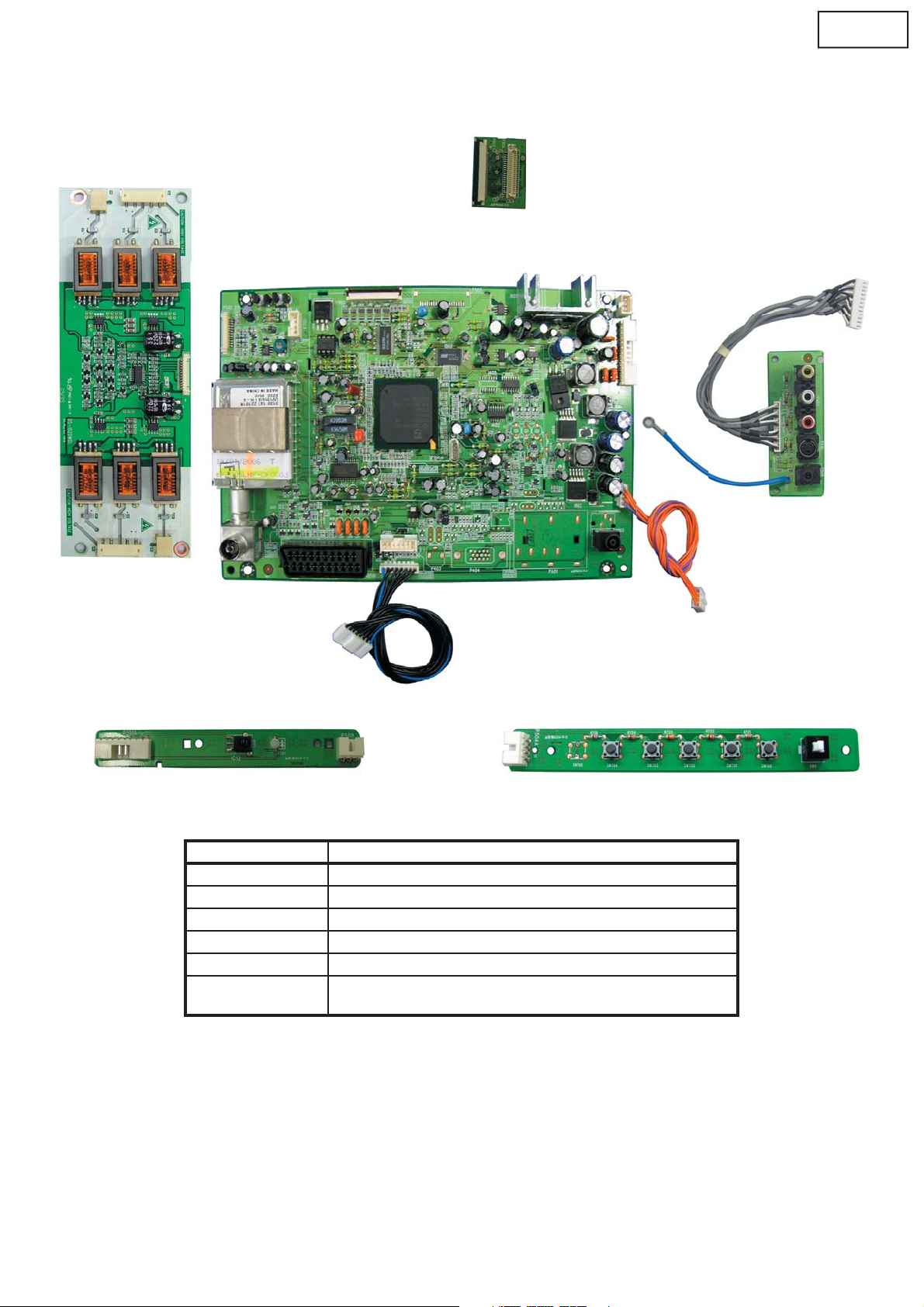
5. Chassis Board Layout
TX-20LB5F/G
TX-20LB5P/G
TTL ASSY
INVERTER
AV ASSY
MAIN ASSY
LED ASSY CTRL ASSY
Board Name Function
MAIN ASSY Main Board
CTRL ASSY Power Switch, Select Switch
AV ASSY AV, Headphone
LED ASSY Remote Receiver, LED, Speaker(R) connection
TTL ASSY Transistor-Transistor Logic circuit
INVERTER Inverter
None serviceable and should be exchanged for service.
7

TX-20LB5F/G
TX-20LB5P/G
6. Before servicing
6.1. Wire dressing
Check a wire dressing is same as illustrated below;
3
P508
4850712S01
A B
P502-INVERTER Coupler Wire
P502
P902
3
P501A
P504A
4859004560
P902-LCD PANEL FFC Cable
P601
PA09 A
2
P504
1
PA09
A
4850703S50
C
P601-Speaker(L) Coupler Wire
4850712N12
D
PA09-PA09A Coupler Wire
4850703S51
E F G
P508-Speaker(R) Coupler
6.1.1 Connection
1. Conect every connector surely as ilustrated above photo (
2. Manage wires not to touch any sharp edge of the metal parts.
3. Manage wires not to have too much tension.
6.1.2 Clamping
Clamp
Wire
P501 - P501A
connection wire
P502 - INVERTER
connection wire
P504 - P504A
connection wire
P508 - Right speaker
connection wire
P601 - Left speaker
connection wire
PA09 - PA09A
connection wire
Wire
CLAMP WIRE
4850708S02
P501-P501A Coupler Wire
1
A
2
TIE CABLE
~ G).
4850704G06
P504-P504A Coupler Wire
3
FILAMENT TAPE
Remark
No clamping
8
TX-20LB5F/G
TX-20LB5P/G
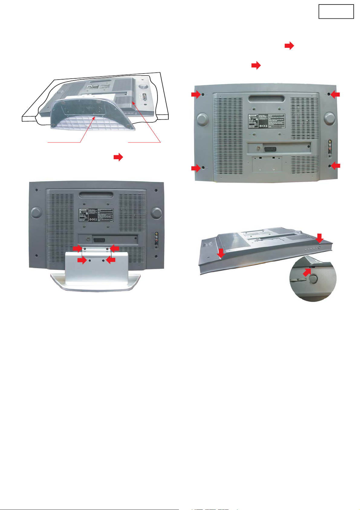
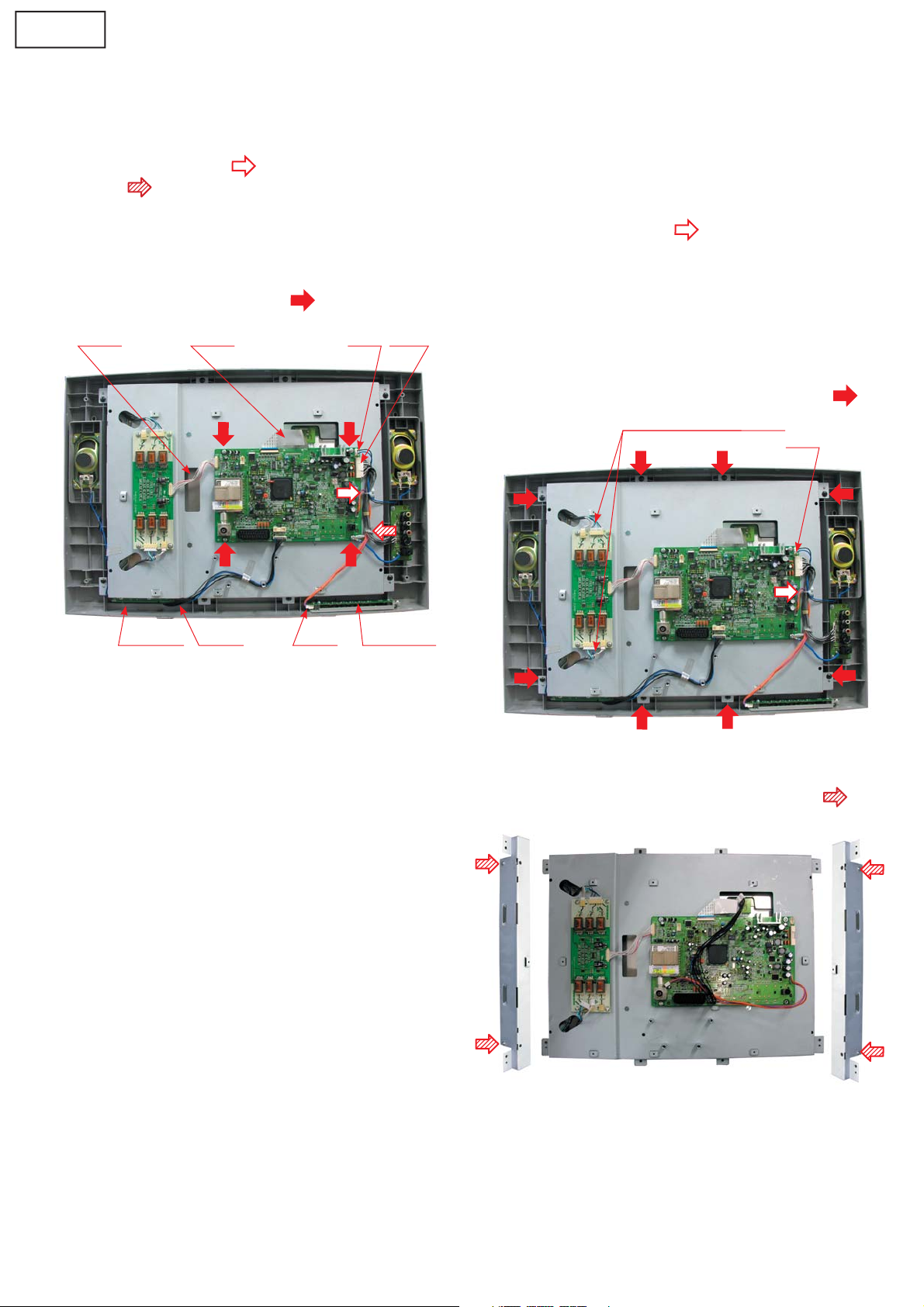
7. Disassembly for service
7.1 Stand Ass’y
1. Lay down the main unit so that the back cover faces
upward.
stand ass’y back cover
2. Remove the fixing screws (4pcs
3. Remove the stand ass’y
)
7.2. Back cover
1. Remove stand ass’y (see 7.1.)
2. Remove the fixing screws (4pcs
3. Remove the Back cover as pushing clips as illustrated
below (2 point clip
)
)
9
TX-20LB5F/G
TX-20LB5P/G
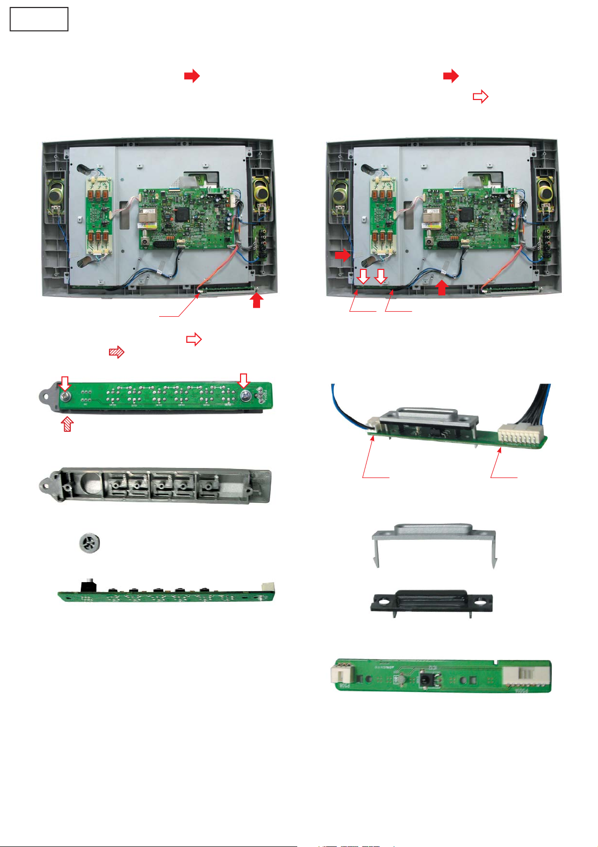
7.3. CTRL Ass’y
1. Remove the back cover (see. 7.2.)
2. Remove the fixing screw (1pcs
3. Remove the CTRL Ass’y with cable
4. Disconnect the coupler (conncector P504)
P504
5. Remove the fixing screws (2pcs
Power (1pcs
)
)
) and Button
7.4. LED Ass’y
1. Remove the back cover (see. 7.2.)
2. Remove the tapes (2pcs
3. Remove the fixing screws (2pcs
4. Remove the LED Ass’y with cable
SP02A P501
5. Disconnect the couplers.
(connector P501 and CONN As SP02A)
)
)
6. Remove the CTRL PCB.
SP02A P501
6. Remove the LED PCB.
10
TX-20LB5F/G
TX-20LB5P/G
7.5. AV Ass’y
1. Remove the back cover (see. 7.2.)
2. Remove tie cable(1pcs
(1pcs
3. Disconnect the coupler (connector PA09)
4. Remove the fixing screws (3pcs
5. Remove the AV Ass’y
) to free the cable.
) and unlock the clamp wire
)
7.6. INVERTER
1. Remove the back cover (see. 7.2.)
2. Disconnect the coupler(connector P502A)
3. Disconnect the backlight interface connectors which
are introduced from LCD panel.
4. Remove the fixing screw (4pcs
backlight interface connector
)
PA0 9
7.7. TTL Ass’y
1. Remove the back cover (see. 7.2.)
2. Unlock the coupler(CONN WAFER P902) to free the
FFC cable(P902A).
3. Remove the TTL Ass’y with FFC cable.
FFC CABLE
P502A
5. Remove the INVERTER.
7.8. Speaker (left and right)
1. Remove the back cover (see. 7.2.)
2. Remove the LED Ass’y (see 7.4.)
3. Remove tie cable(1pcs
pler (CONN AS SP01A)
4. Remove the fixing screws (8pcs
5. Remove the speaker (left and right).
) and disconnect the cou-
)
SP02
4. Unlock the coupler(CONN WAFER P905) and remove
FFC cable.
FFC CABLE
5. Remove the TTL Ass’y.
P905
LED Ass’y
11
TX-20LB5F/G
TX-20LB5P/G
7.9. Main Ass’y
1. Remove the back cover (see. 7.2.)
2. Remove the LED Ass’y, CTRL Ass’y
(see 7.3., 7.4.)
3. Remove tie cable(1pcs
(1pcs
4. Disconnect the couplers (connector P902A, SP01A,
PA09A, P504A, P501A)
5. Disconnect the FFC cable(P902A)
6. Remove the fixing screws (4 pcs
P502A P902A SP01A PA09A
) to free the cable.
) and unlock the clamp wire
)
7.10. Panel LCD
1. Remove the back cover (see. 7.2.)
2. Remove the TTL Ass’y (see 7.7.)
3. Disconnect the backlight interface connectors which
are introduced from LCD panel
4. Remove the LED Ass’y (see 7.4.)
5. Remove tie cable (1pcs
6. Disconnect left speaker wire (connector SP01A)
7. Remove the fixing screws from AV Ass’y
(3 pcs, see 7.5.4.)
8. Remove the fixing screw from CTRL Ass’y
(1 pcs, see 7.3.2.)
9. Remove the fixing screws from Frame Main (8 pcs
backlight interface connector
)
)
SP01A
CTRL Ass’yP504AP501ALED Ass’y
10. Take out Frame Main with Panel.
11. Remove screws from Frame Main PCB (4 pcs
)
12
 Loading...