

Panasonic TX-17LX2, TX-17LX2F Service manual

Service Manual
LCD TV
CHASSIS : SL-115P
MODEL :
TX-17LX2(UK)
TX-17LX2F(EUROPE)
Power Source
“AC 100-240V, 50/60Hz”
Power Consumption
Average use : 50W
Stand-by condition : 3w
“TV set DC 15v, 1.2A max”
LCD
“17-inch(434.38mm), 15:9
aspect ratio LCD panel”
Screen Size
372.48mm(H) * 223.488mm(V)
Sound
Speaker
“5cm * 9cm, 2pcs, 4
”
Audio Output
“5W(2.5W+2.5W), 10%THD”
Headphones
M3(3.5mm) Jack * 1
Receiving Systems / Band name
“PAL B, G, H, SECAM B, G, SECAM L/L”
VHF E2-E12
VHF H1-H2(ITALY)
VHF A-H(ITALY)
UHF E21-E69(UK only)
CATV(S01-S05)
CATV S1-S10 (M1-M10)
CATV S11-S20 (U1-U10)
CATV S21-S41 (Hyperband)
PAL 525/60
Playback of NTSC tape from
some PAL video recorders
(VCR)
M.NTSC
Playback From M.NTSC video
recorders (VCR)
NTSC (AV input only)
Playback From NTSC video
recorders (VCR)
Aerial-ear
UHF(UK only)/VHF
Operating Conditions
Temperature : 5-35°…
Humidity : 5%-90% RH (noncondensing)
Connection Terminals
AV1 (Scart connecter)
“21 Pin socket (Audio/Video
in, Audio/Video out, RGB in)”
AV2
VIDEO
RCA PIN Type * 1
S-VIDEO
Mini DIN 4-pin
AUDIO L-R
RCA PIN Type * 2
Dimensions (W * H * D)
Including TV Stand
532mm * 297mm * 190mm
TV Set Only
532mm * 297mm * 68mm
Weight (Mass)
6.2Kg NET
Note :
DSL115PEF0
2003 Matsushita Electric Industrial Co., Ltd.
All rights reserved. Unauthorized copying and
distribution is a violation of law.
1. Safety Precautions 2
1.1 General Guidelines 2
1.2 Touch-Current Check 2
2. Prevention of Electro Static Discharge(ESD) to
Electrostatically Sensitive(ES) Devices 3
3. Chasis Board Layout 4
4. Servicing method 5
4.1 Removing the tilt base 5
4.2 Removing the rear cover 5
4.3 Removing the Switch Unit 6
4.4 Removing the C-Board 6
4.5 Removing the E-Board 6
4.6 Removing the F-Board 6
4.7 Removing the D-Board 7
4.8 Removing the Speaker Unit 7
4.9 Removing the BRKT hinge 7
4.10 Removing the Shield pcd assy 7
4.11 Removing the LCD Panel 8
4.12 Removing the A-Board, B-Board 8
5. Service Mode Function 9
5.1 How to enter SERVICE 1 9
1
Design and Specifications are subject to change without notice.
Weight and Dimensions shown are approximate.
WARNING
This service information is designed for experienced repair technicians only and is not designed for use by the general public.
It does not contain warnings or cautions to advise non-technical individuals of potential dangers in attempting to service a product.
Products powered by electricity should be serviced or repaired only by experienced professional technicians. Any attempt to service
or repair the product or products dealt with in this service information by anyone else could result in serious injury or death.
6. Conductor Views 10
6.1 MAIN PCB(TOP) 10
6.2 MAIN PCB(BOTTOM) 11
7. Block and Schematic Diagrams 12
7.1 Schematic Diagram Notes 12
7.2 Power Block Diagram 13
7.3 Power Block Diagram 14
7.4 VCTI Block Diagram 15
7.5 Input Block Diagram 16
7.6 Memory AMP Schematic Diagram 17
7.7 AD9883 Schematic Diagram 18
7.8 Deinterlace Schematic Diagram 19
7.9 SDRAM Schematic Diagram 20
7.10 Image Processor Schematic Diagram 21
7.11 LVDS, KEY Schematic Diagram 22
8. Parts Location & Mechenical Replacement
Parts List 23
8.1 Part Location 23
8.2 Packing Exploded View 24
9. Service Parts List 25
Contents
2
1. Safety Instruction
1.1. General Guidelines
1. When servicing, observe the original lead dress. If a short circuit is found, replace all part
which have been overheated or damaged by the short circuit.
2. After servicing, see to it that all the protective devices such as insulation barriers,
insulation papers shields are properly installed.
3. After servicing, make the following leakage current checks to prevent the customer from
being exposed to shock hazards.
1.2. Touch-Current Check
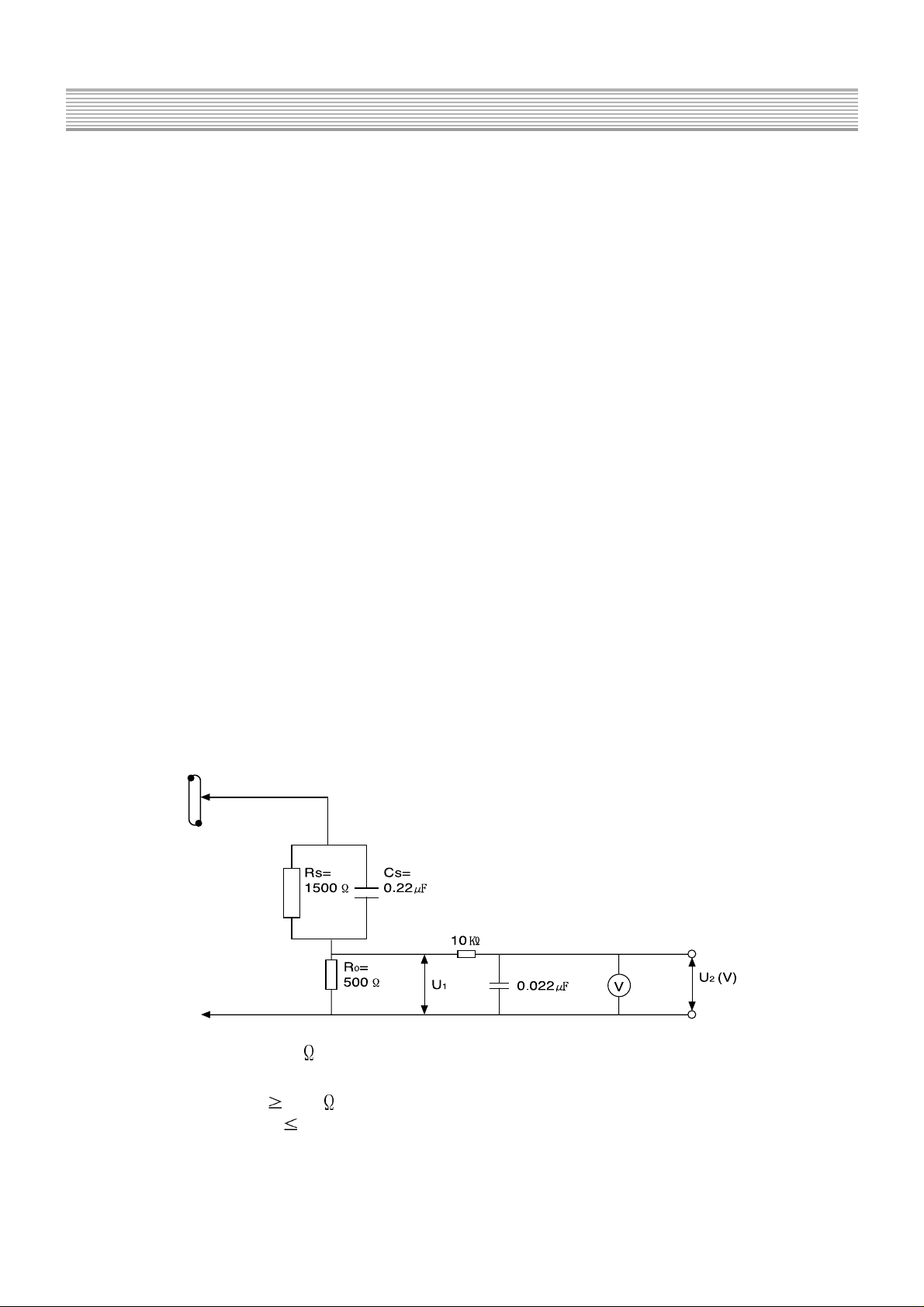
1. Plug the AC cord directly into the AC outlet. Do not use an isolation transformer for this chack.
2. Connect a measuring network for touch currents between each exposed matallic part on
the set and a good earth ground such as a water pipe, as shown in Figure1.
3. Use Leakage Current Tester(Simpson 228 or equivalent) to measure the potential across
the measuring network.
4. Check each exposed metallic part, and measure the voltage at each point.
6. The potential at any point (TOUGH CURRENT) expressed as voltage U1 and U2, does not
exceed the following values:
For a. c.: U1 = 35V(peak) and U2 = 0.35V(peak);
For d. c.: U1 = 1.0V,
Note:
The limit value of U
2 = 0.35V(peak) for a. c. and U1
= 1.0V for d. c. correspond to the
values 0.7 mA (peak) a. c. and 2.0 mA d. c.
The limit value U
1 = 35V(peak) for a. c. correspend to the value 70 mA(peark) a. c. for
frequencies greater than 100kHz.
7. In case a measurement is out of the limits specified, there is a possibility of a shock hazard, and the
equipment should be repaired and rechecked before it is returned to the customer.
Measuring network for TOUCH CURRENTS
Resistance values in ohms( )
V: Voltmeter or oscilloscope(r.m.s. or peak reading)
Input resistance: 1M
Input capacitance: 200 pF
Frequency range: 15Hz to 1 MHz and d.c. respectively
NOTE - Appropriate measures should be taken to obtain the correct value in case of non-
sinusoidal waveforms.
Figure 1
COLD
WATER PIPE
(EARTH
GROUND
TO
APPLIANCES
EXPOSED
METAL PARTS
3
2 Prevention of Electro Static Discharge (ESD) to Electrostatically Sensitive(ES) Devices
Some semiconductor (solid state) devices can be damaged easily by static electricity. Such
components commonly are called Electrostatically Sensitive (ES) Devices. Examples of typical
ES devices are integrated circuits and some field-effect transistors and semiconductor “chip”
components. The following techniques should be used to help reduce the incidence of
component damage caused by electro static discharge(ESD).
1. Immediately before handling any semiconductor component or semiconductor-equipped
assembly, drain off any ESD on your body by touching a known earth ground. Alternatively,
obtain and wear a commercially available discharging ESD wrist strap, which should be
removed for potential shock reasons prior to applying power to the unit under test.
2. After removing an electrical assembly equipped with ES devices, place the assembly on a
conductive surface such as alminum foil, to prevent electrostatic charge buildup or exposure
of the assembly.
3. Use only a grounded-tip soldering iron to solder or unsolder ES devices.
4. Use only an anti-static solder removal device. Some solder removal devices not classified as
“anti-static(ESD protected)” can generate electrical charge sufficient to damage ES devices.
5. Do not use freon-propelled chemicals. These can generate electrical chages sufficient to
damage ES devices.
6. Do not remove a replacement ES device from its protective package until immediately before
you are ready to install it.(Most replacement ES devices are packaged with leadse
electrically shorted together by conductive foam, alminum foil or comparable conductive
material).
7. Immediately before removing the protective material from the leads of a replacement ES
device, touch the protective material to the chassis or circuit assembly into which the device
will be installed.
Caution
Be sure no power is applied to the chassis or circuit, and observe all other safety
precautions.
8. Minimize bodily motions when handling unpackaged replacement ES devices. (Otherwise
hamless motion such as the brushing together of your clothes fabric or the lifting of your foot
from a carpeted floor can generate static electricity (ESD) sufficient to damage an ES
device).
There are special components used in this epuipment which are imporant for safety.
These parts are maked by in the schematic diagrams, Exploded Views and replacement parts list. lt is
essential that these critical parts should be replaced with manufacturer’s specified parts to prevent shock,
fire, or other hazards. Do not modify the original design without permission of manufacturer.
IMPORTANT SAFETY NOTICE
4
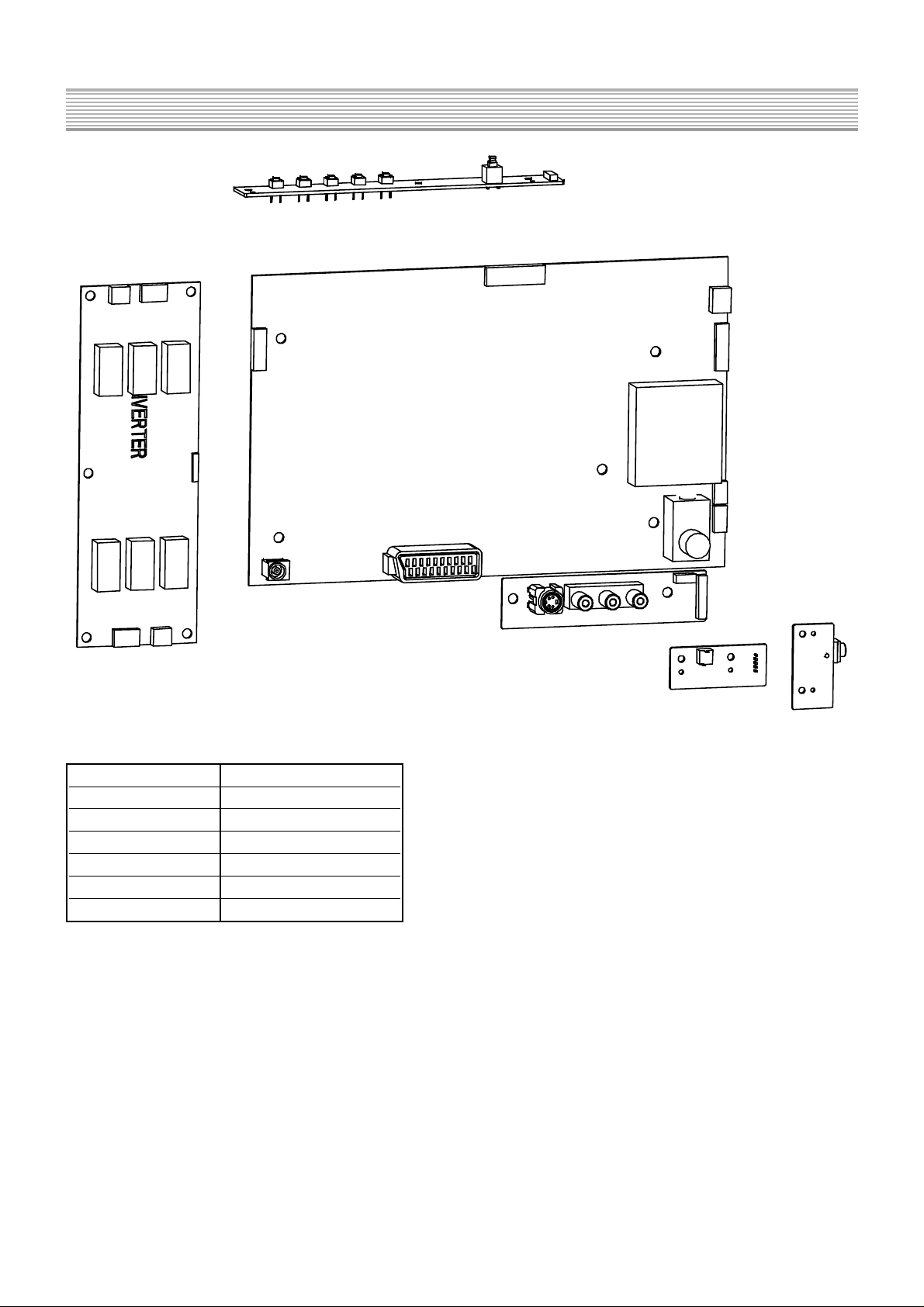
3. Chasis Board Layout
A
C
D
E
F
B
Board Name Function
A-Board MAIN PCB
B-Board INVERTER PCB
C-Board
CONTROL PCB
D-Board AV PCB
E-Board E/PHONE PCB
F-Board IR/LED PCB
5
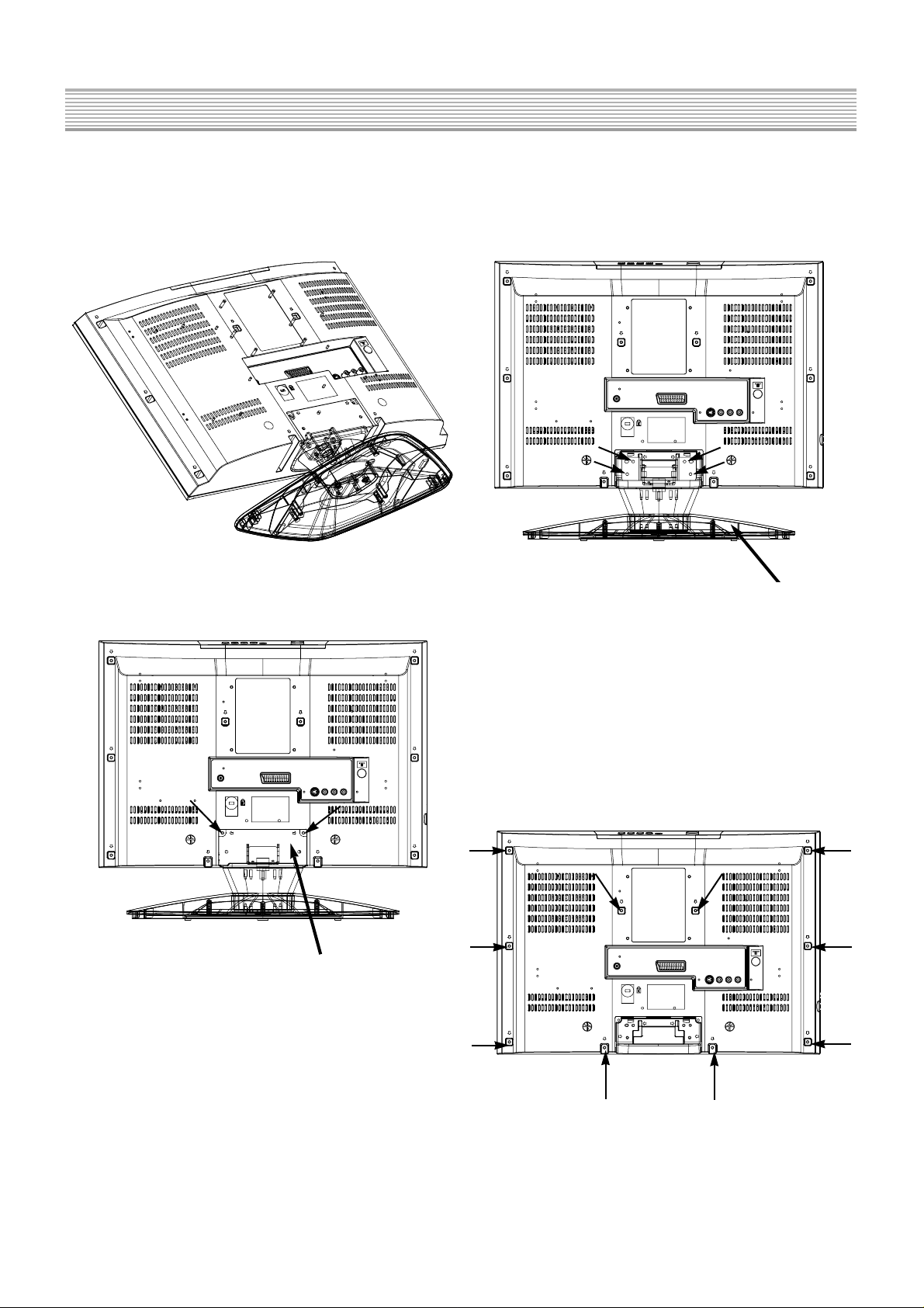
4. Servicing method
4.1. Removing the tilt base
1. Lay down the main unit so that the rear
cover faces upward.
2. Remove the fixing screw(2pcs).
3. Remove the hinge cover.
4. Remove the fixing screws(4pcs).
5. Remove the tilt base.
4.2. Removing the rear cover
1. Remove the tilt base.(See 5.1.)
2. Remove the fixing screw(10pcs)
3. Remove the rear cover.
Hinge cover
Tilt base
6
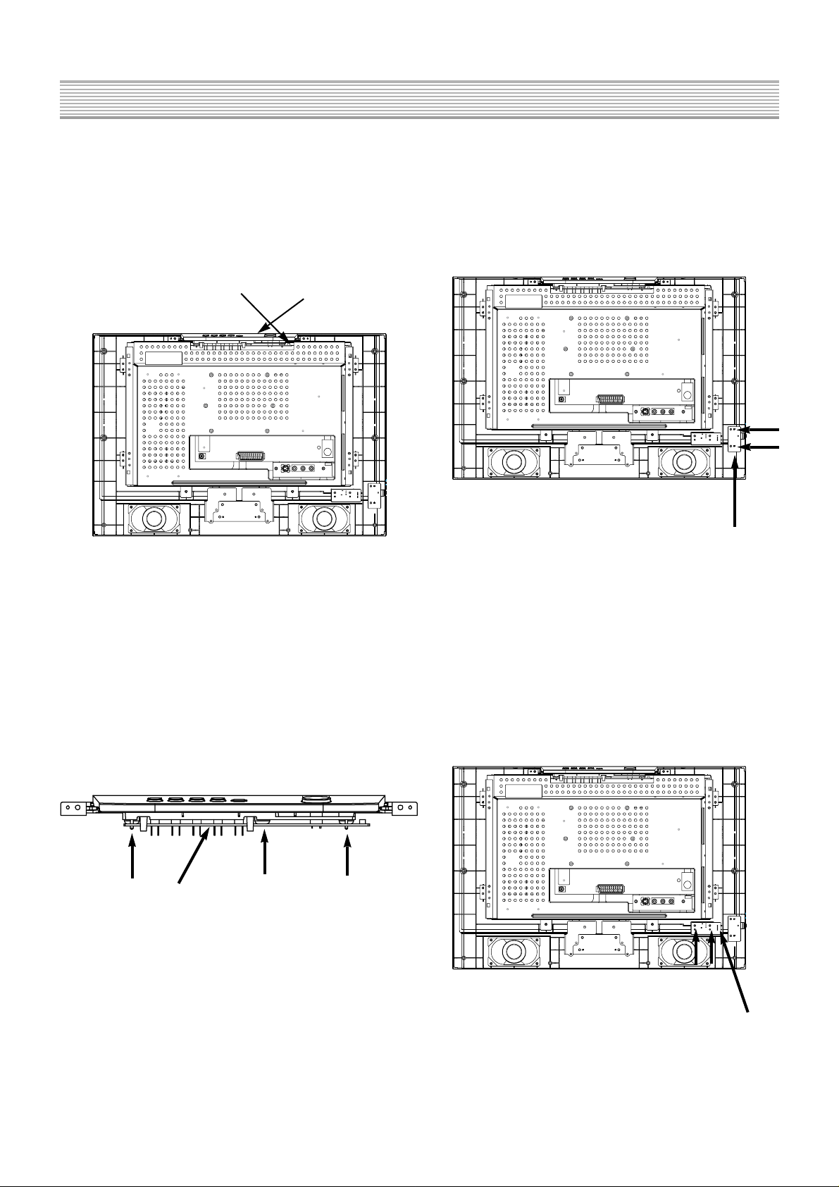
Servicing method
4.3. Removing the switch unit
1. Remove the rear cover(See 5.2.)
2. Disconnect the coupler(C1).
3. Remove the fixing screws(2pcs).
4. Remove the switch unit.
4.4. Removing the C-Board
1. Remove the switch unit(See 5.3.)
2. Remove the fixing screws(3pcs)
3. Remove the C-Board.
4.5. Removing the E-Board
1. Remove the rear cover(See 5.2.)
2. Disconnect the coupler(E1).
3. Remove the fixing screws(2pcs).
4. Remove the E-Board.
4.6. Removing the F-Board
1. Remove the rear cover(See 5.2.)
2. Disconnect the coupler(F1).
3. Remove the fixing screws(2pcs).
4. Remove the F-Board.
Swich unita
Coupler(C1)
C-Board
Coupler(E1)
Coupler(F1)
7
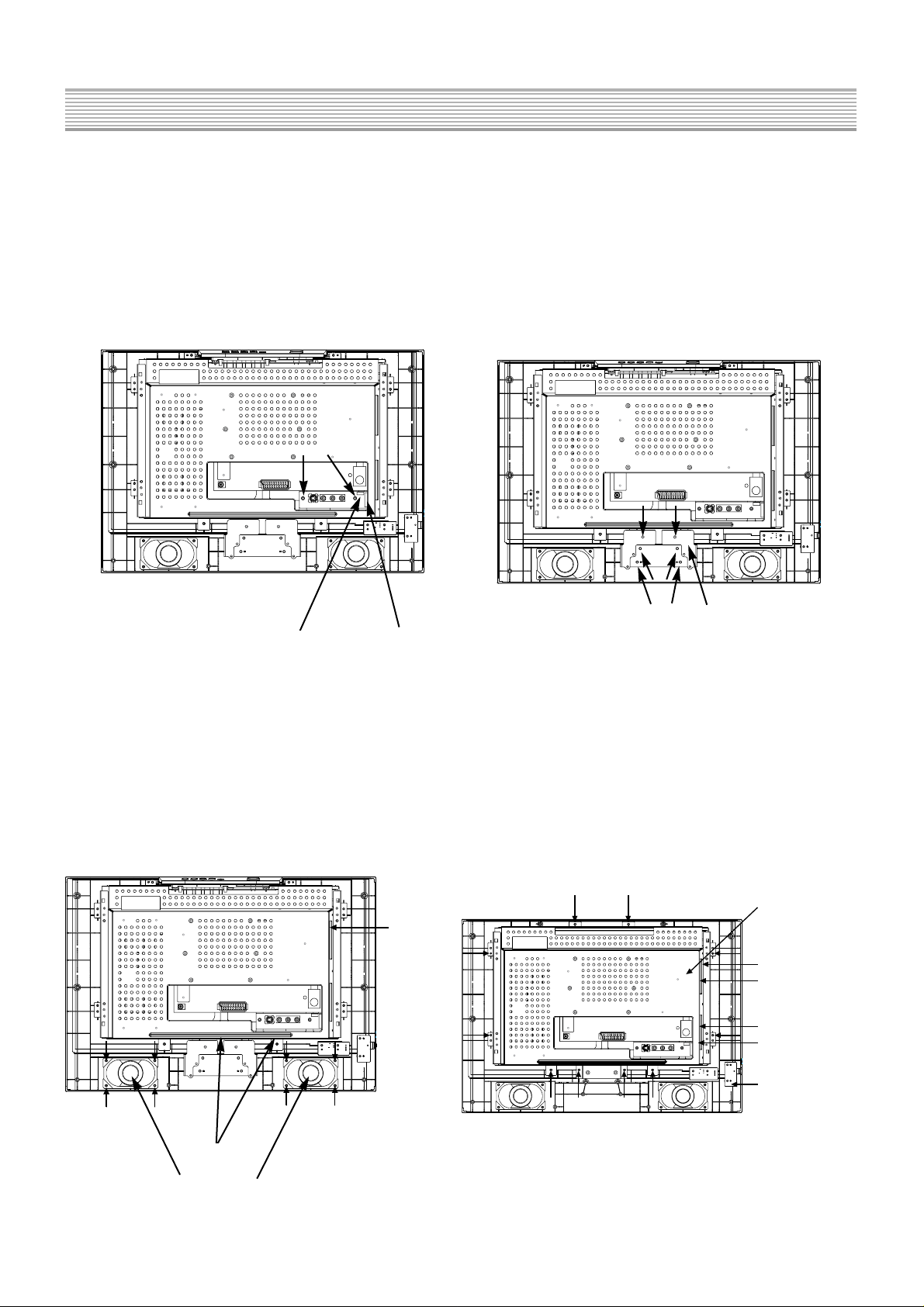
Servicing method
4.7. Removing the D-Board
1. Remove the rear cover(See 5.2.)
2. Disconnect the coupler(D1,D2).
3. Remove the fixing screws(2pcs).
4. Remove the D-Board.
4.8. Removing the Speaker unit
1. Remove the rear cover(See 5.2.)
2. Remove the fixing screws(8pcs).
3. Disconnect the coupler(A1), and unlock the
cable clamper and hook to free the cable.
4. Remove the speaker units.
4.9. Removing the BRKT hinge
1. Remove the rear cover(See 5.2.)
2. Remove the fixing screws(6pcs).
3. Remove the BRKT hinge.
4.10. Removing the Shield pcb assy.
1. Remove the Switch unit(See 5.3.)
2. Remove the BRKT hinge(See 5.9.)
3. Remove the fixing screws(10pcs).
4.Disconnect the coupler (A1), (A2), (A3),
(A4), (E1).
5. Remove the Shield pcb assy.
Coupler(A1)
Shield pcb assy
Coupler(A1)
Coupler(A2)
Coupler(A3)
Coupler(A4)
Coupler(E1)
Coupler(D1)Coupler(D2)
Clamper
Speaker
BRKT hinge
8
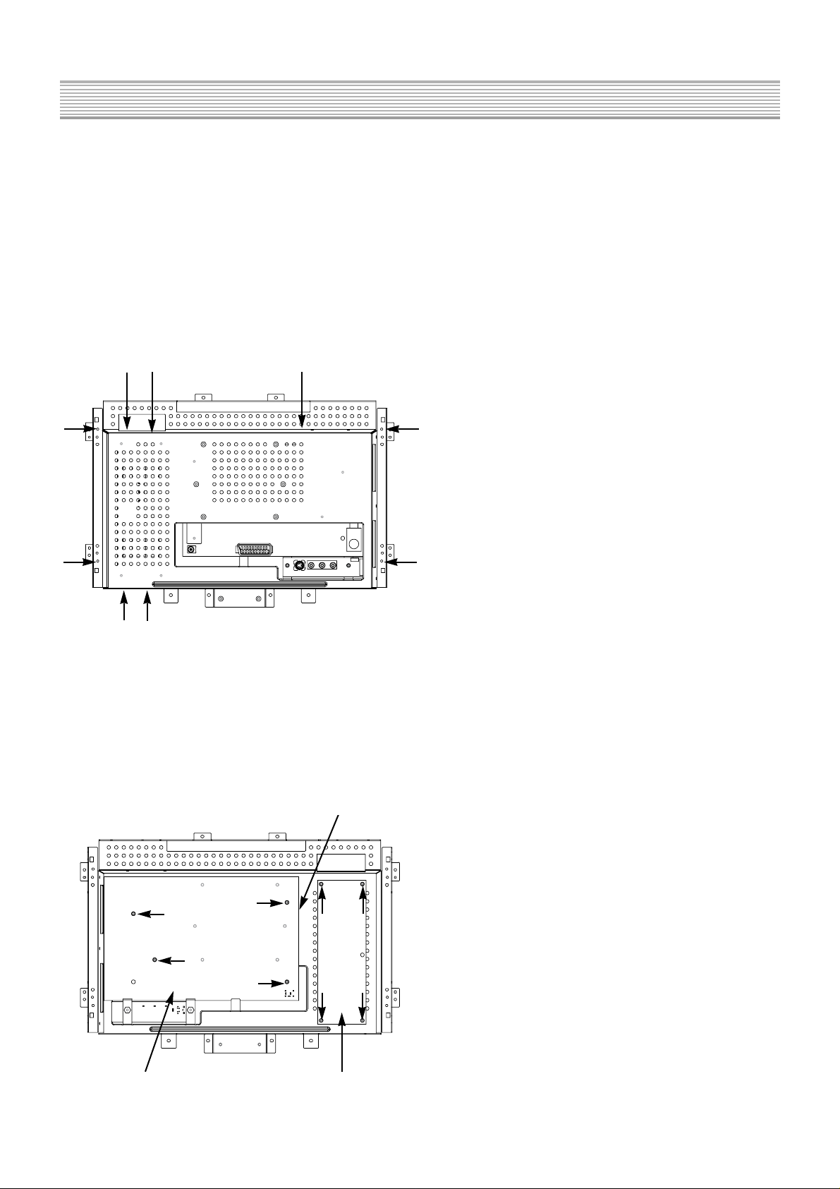
Servicing method
4.11. Removing the LCD panel.
1. Remove the Shield pcb assy.(See 5.10.)
2. Remove the fixing screws(4pcs).
3. Disconnect the coupler (A5), (B1), (B2),
(B3), (B4).
4. Remove the LCD panel.
4.12. Removing the A-board, B-board.
1. Remove the LCD panel.(See 5.11.)
2. Remove the fixing screws(8pcs).
3. Disconnect the coupler(A6).
4. Remove the A-board, B-board.
Coupler(B1),(B2)
Coupler(B3),(B4) Coupler(A5)
Coupler(A6)
B-boardA-board
9
5. Service Mode Function
The following setting and adjustment can be adjusted by remote control in Service Mode.
6.1. How to enter SERVICE 1
1. Set the channel to CH99.
2. Press HOLD button on remote control.
Note: To exit to Service mode, press N or Power button on remote control.
99
Panel R Drive
G Drive
B Drive
Set for UK<Yes>
Key Command
Press the top and bottom key,and
select the functions.
Use left and right key to control the
function values.
 Loading...