

Page 1
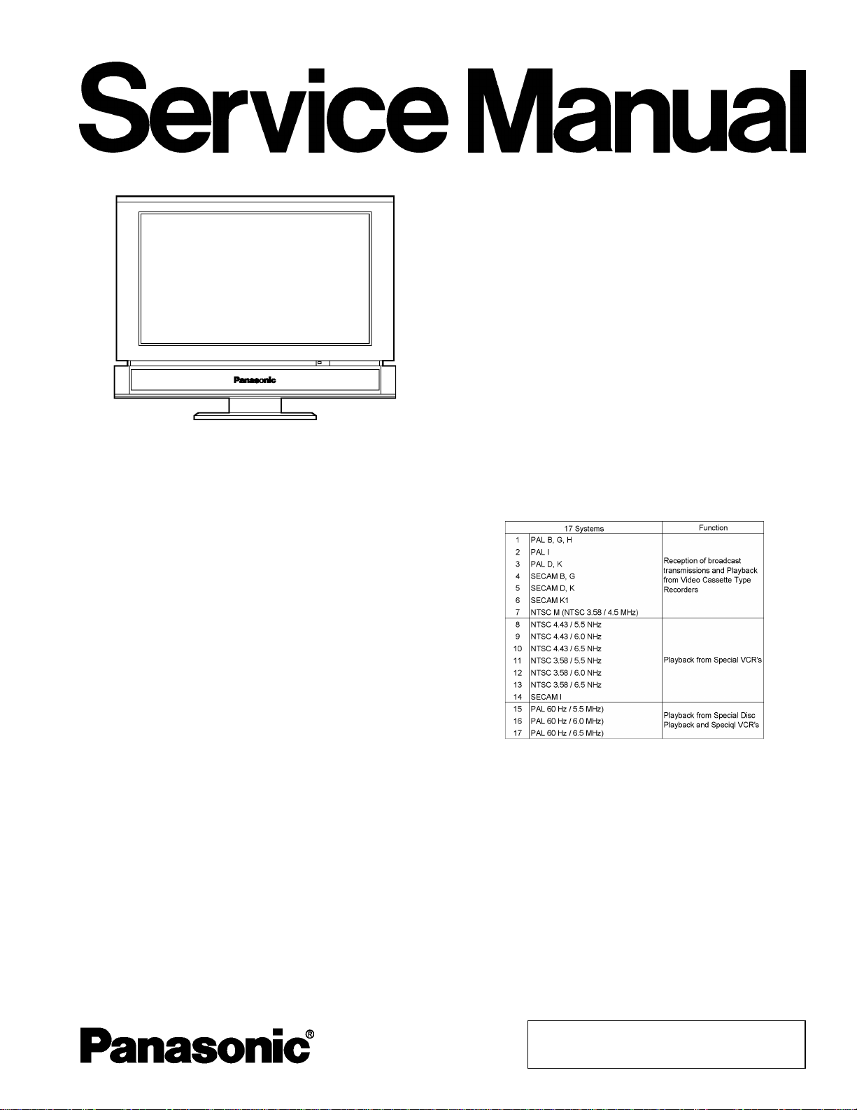
15.2” Diagonal LCD TV
TX-15LT2M
TX-15LT2Q
TX-15LT2Z
TX-15LT2X
TX-15LT2T
LH1 Chassis
ORDER NO. ITD0303001C2
Specifications
Power Source
AC 100~240V, 50/60Hz
Power Consumption
Average use: 49W
Stand-by condition: 4W
TV set: DC 15V, 2.8 A max.
LCD
15.2-inch (385mm), 16:9 aspect ratio LCD panel
Screen Size
13.21-inch (335.6mm) (W) x 7.43-inch (188.6mm)(H) x 15.2inch (385.0mm)(Diagonal)
Sound
Speaker
Tweeter (3 x 4cm 2pcs, 89), Woofer (Ø5cm, 89)
Audio Output
6.5W (2.0W+2.0W+2.5W (Woofer)), 10%THD
Headphones
M3(3.5 mm) Jack x 1 89 impedance
FEATURES
Aero-Hammer®Woofer System (2Way 3Speaker System)
Receiving System
Receiving Channels
Regular TV
VHF BAND
2-12 (PAL/SECAM B, K1)
0-12 (PAL B AUST.)
1-9 (PAL B N.Z)
1-12 (PAL/SECAM D)
1-12 (NTSC M Japan)
2-13 (NTSC M U.S.A)
UHF BAND
21-69 (PAL G, H, I/SECAM G, K, K1)
28-69 (PAL B AUST.)
13-57 (PAL D, K)
© 2003 Matsushita Electric Industrial Co., Ltd. All
rights reserved. Unauthorized copying and
distribution is a violation of law.
Page 2
TX-15LT2M / TX-15LT2Q / TX-15LT2Z / TX-15LT2X / TX-15LT2T
13-62 (NTSC M Japan)
14-69 (NTSC M U.S.A)
14-69 (NTSC M U.S.A)
CATV
S1-S20 (OSCAR)
1-125 (U.S.A CATV)
C13-C49 (JAPAN)
S21-S41 (HYPER)
Z1-Z37 (CHINA)
5A, 9A (AUST.)
Aerial-Rear
UHF/VHF
Operating Conditions
Temperature: 5-40°C
Humidity: 5%-90% RH (non-condensing)
Connection Terminals
AV1
21 Pin socket
(Audio/ Video in, TV out, RGB in)
AV2
VIDEO
RCA PIN Type x 1
S-VIDEO
Mini DIN 4-pin
AUDIO L-R
RCA PIN Type × 2
AUDIO OUT
3.5mm, Stereo Jack 0.5Vrms
Dimensions (W x H x D)
Including TV Stand
413mm x 330mm x 180mm
TV Set Only
413mm x 295mm x 73mm
Weight (Mass)
5.6kg Net
Storage Conditions
Temperature: 55°C MAX
Note:
Design and Specifications are subject to change without notice.
Weight and Dimensions shown are approximate.
CONTENTS
1 Safety Precautions
1.1. General Guidelines
2 Prevention of Electro Static Discharge (ESD) to
Electrostatically Sensitive (ES) Devices
3 About lead free solder (PbF)
4SelfCheck
5 SERVICE HINTS
5.1. Hotel Mode
6 Chasis Board Layout
7 Servicing method
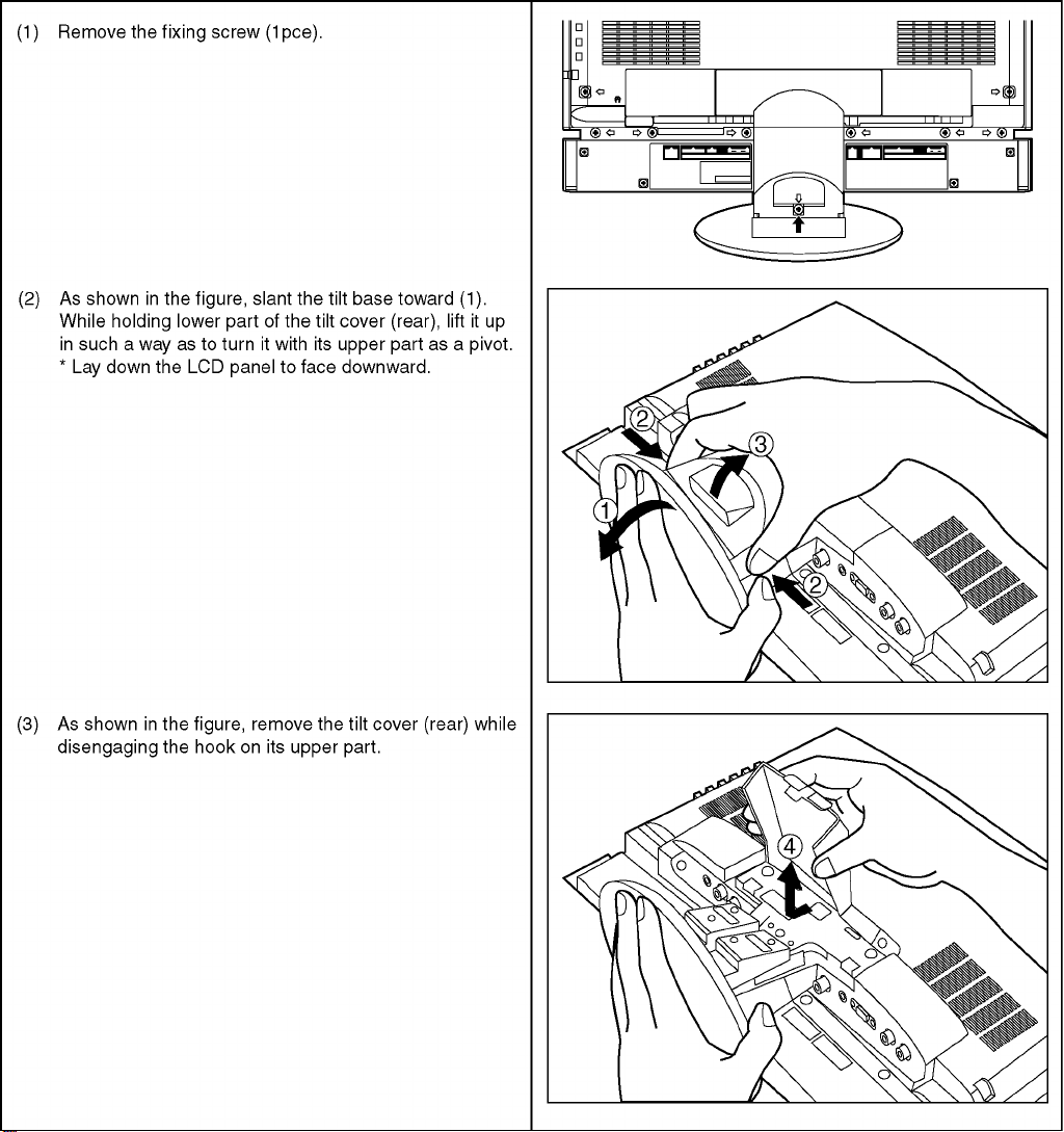
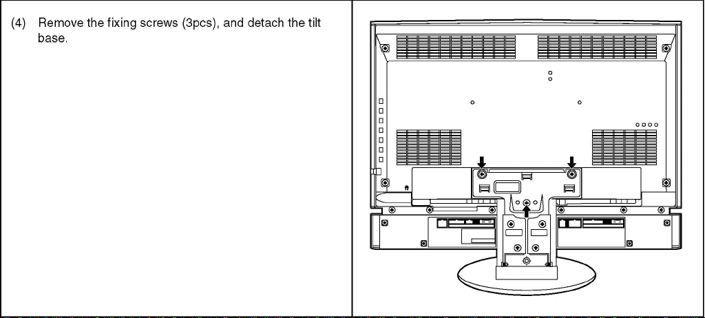
7.1. Removing tilt base
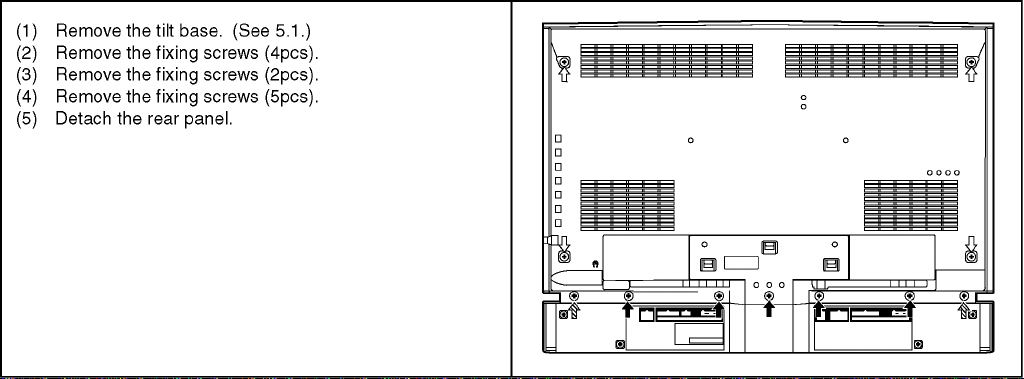
7.2. Removing rear panel
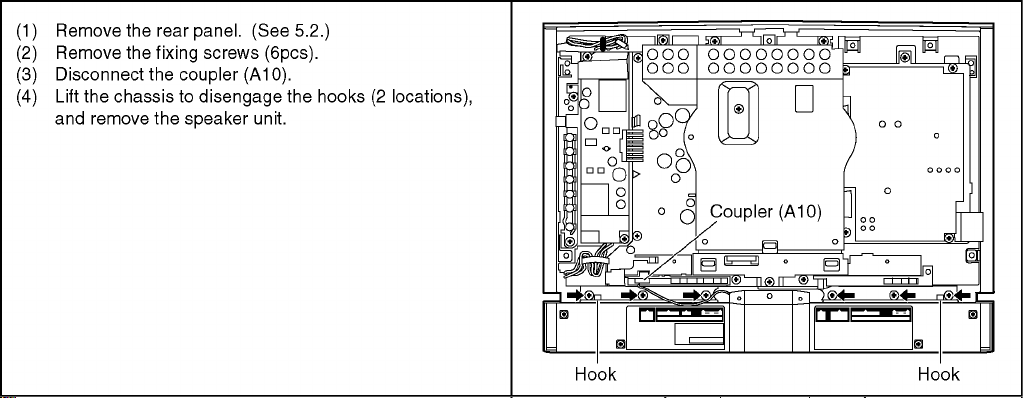
7.3. Removing speaker unit
7.4. Removing front panel
7.5. Removing LCD panel
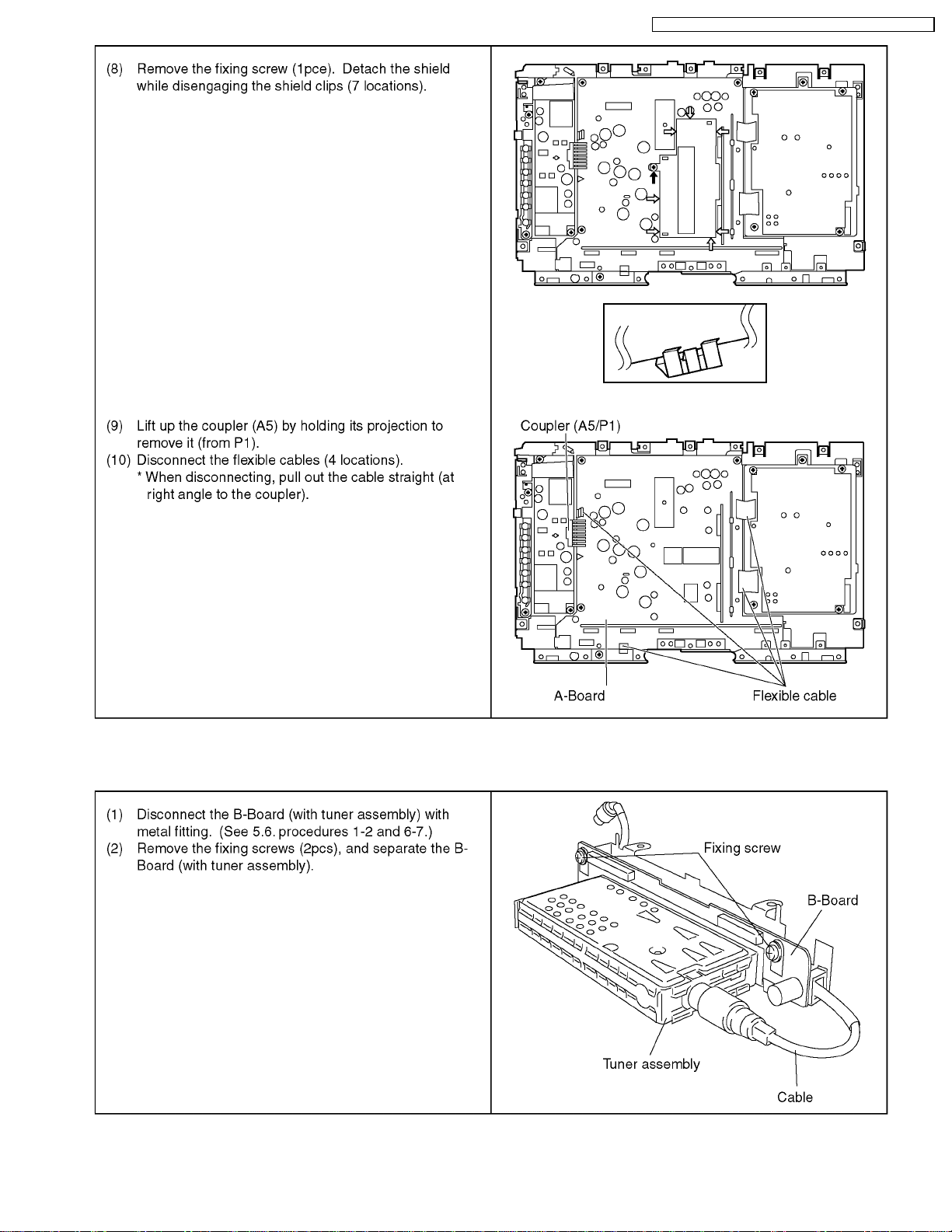
7.6. Removing main A-Board
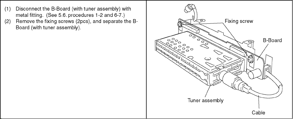
7.7. Removing B-Board (with tuner assembly)
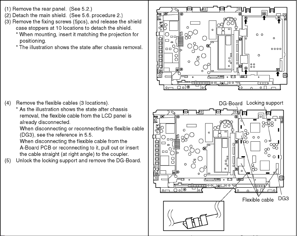
7.8. Removing DG-Board
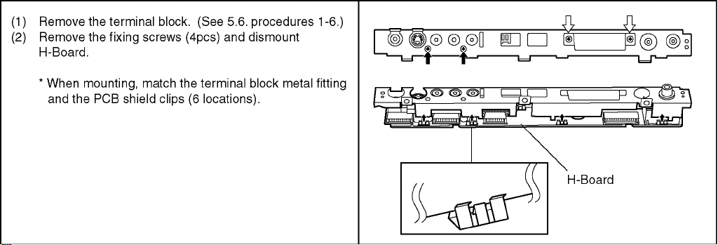
7.9. Removing H-Board
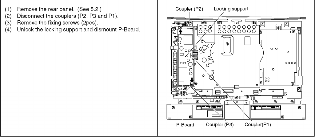
7.10. Removing P-Board
7.11. Removing K-Board
7.12. Pull out the flexible cable straight to the coupler.
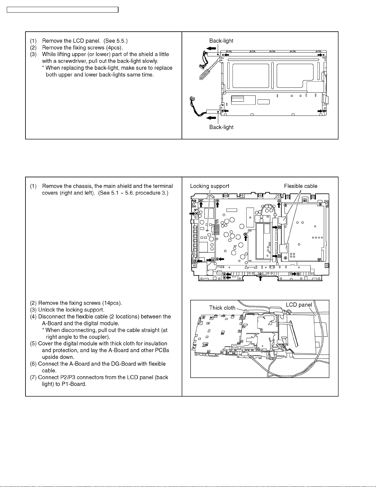
7.13. Removing back-light
7.14. A-Board servicing
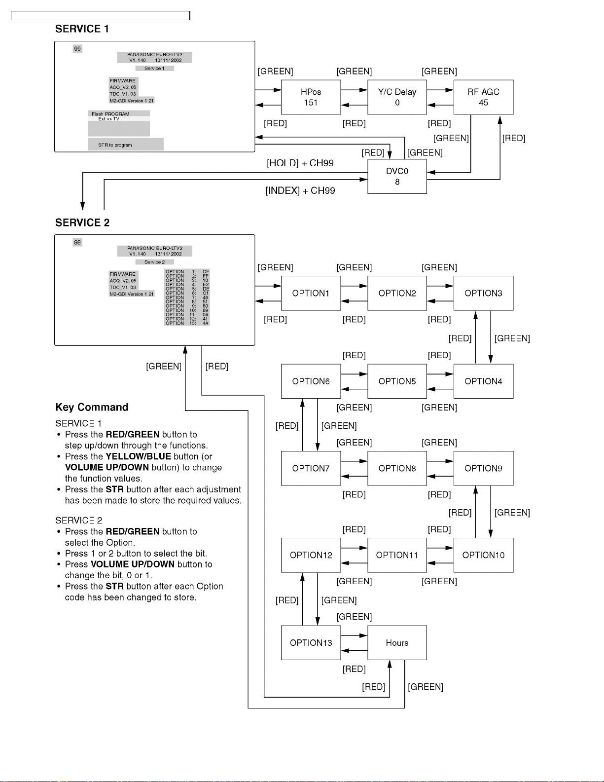
8 Service Mode Function
Page Page
4
4
5
6
7
7
7
8
9
9
10
10
11
11
12
13
14
14
15
15
15
16
16
17
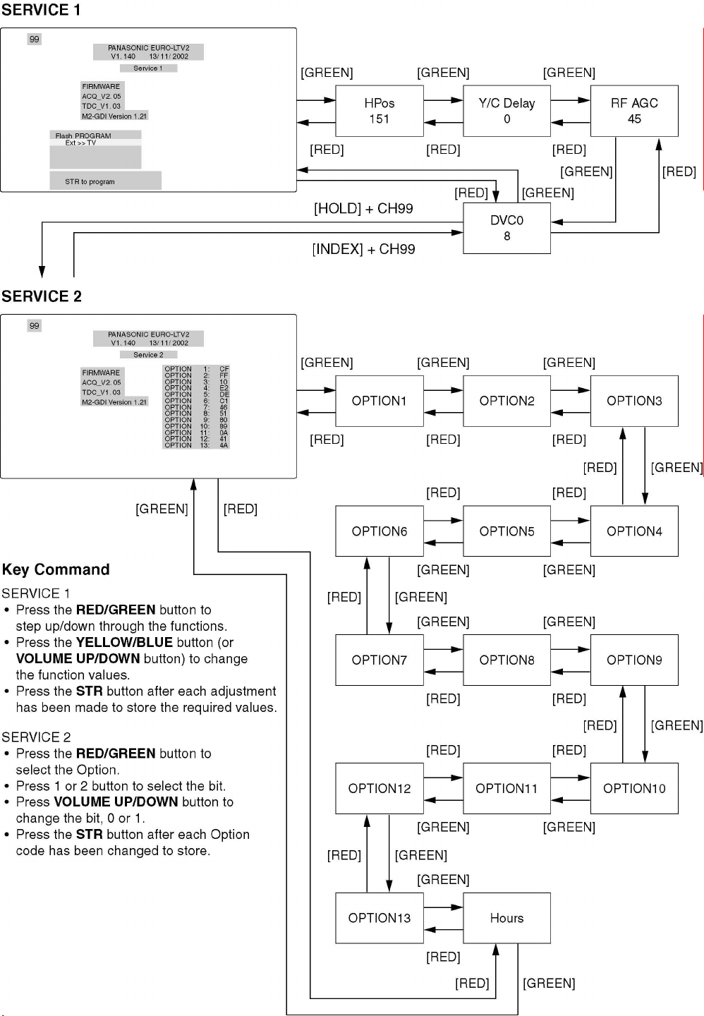
8.1. How to enter SERVICE 1
8.2. How to enter SERVICE 2
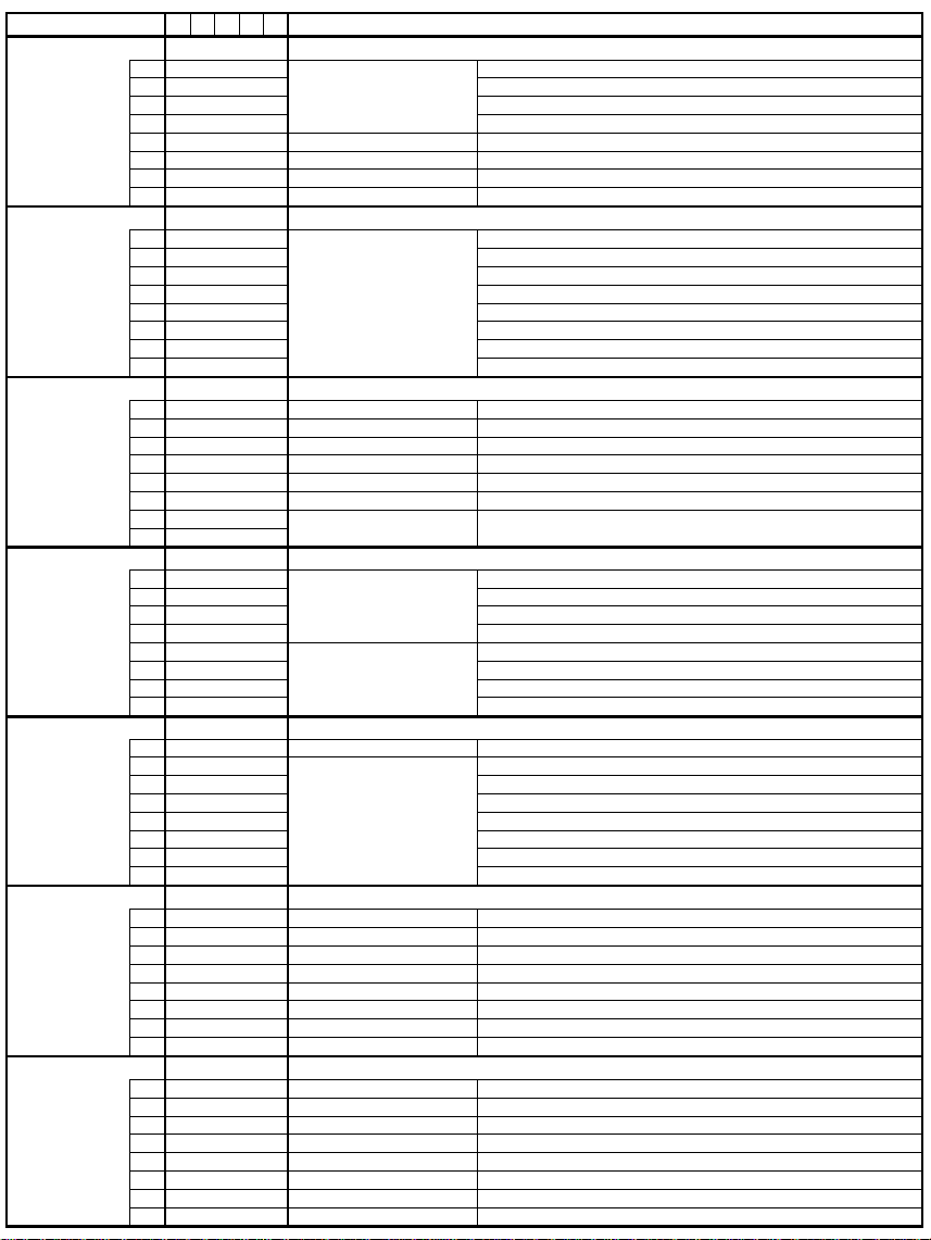
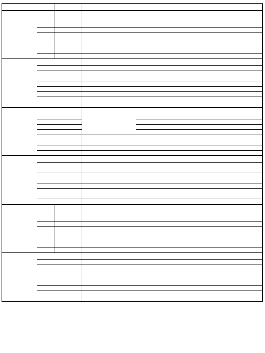
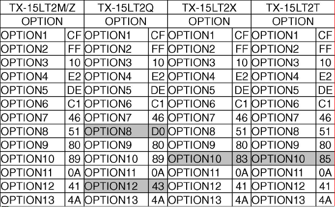
8.3. Option Description
8.4. Option Code Setting
9 Adjustment
9.1. RF AGC Adjustment
9.2. DVCO Adjustment
10 Conductor Views
10.1. A-Board
10.2. B, H, K, P and V-Board
10.3. DG-Board
11 Block and Schematic Diagrams
11.1. Schematic Diagram Notes
11.2. Power Block Diagram
11.3. Signal Block Diagram
11.4. A-Board (1 of 4) Schematic Diagram
11.5. A-Board (2 of 4) Schematic Diagram
11.6. A-Board (3 of 4) Schematic Diagram
11.7. A-Board (4 of 4) Schematic Diagram
11.8. DG-Board (1 of 5) Schematic Diagram
11.9. DG-Board (2 of 5) Schematic Diagram
11.10. DG-Board (3 of 5) Schematic Diagram
11.11. DG-Board (4 of 5) Schematic Diagram
11.12. DG-Board (5 of 5) Schematic Diagram
11.13. B, H, K, and V-Board Schematic Diagram
17
17
19
21
22
22
22
23
23
25
27
29
29
30
32
34
35
36
37
38
39
40
41
42
43
2
Page 3

11.14. P-Board Schematic Diagram 44
12 Parts Location & Mechanical Replacement Parts List
12.1. Parts Location
12.2. Packing Exploded View
12.3. Mechanical Replacement Parts List
45
13 Replacement Parts List
45
46
13.1. Replacement Parts List Notes
13.2. Electrical Replacement Parts List Notes
TX-15LT2M / TX-15LT2Q / TX-15LT2Z / TX-15LT2X / TX-15LT2T
47
48
48
49
3
Page 4
TX-15LT2M / TX-15LT2Q / TX-15LT2Z / TX-15LT2X / TX-15LT2T
1 Safety Precautions
1.1. General Guidelines
1.When servicing, observe the original lead dress. If a short circuit is found, replace all parts which have been overheated or
damaged by the short circuit.
2.After servicing, see to it that all the protective devices such as insulation barriers, insulation papers shields are properly
installed.
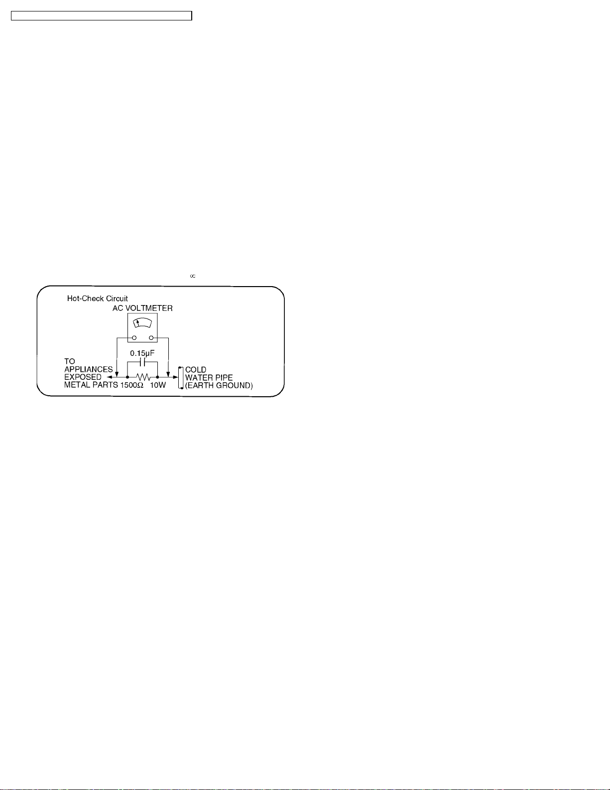
3.After servicing, make the following leakage current checks to prevent the customer from being exposed to shock hazards.
1.1.1. Leakage Current Cold Check
1.Unplug the AC cord and connect a jumper between the two
prongs on the plug.
2.Measure the resistance value, with an ohmmeter, between
the jumpered AC plug and each exposed metallic cabinet
part on the equipment such as screwheads, connectors,
control shafts, etc. When the exposed metallic part has a
return path to the chassis, the reading should be between
1M9 and 5.2M9.
When the exposed metal does not have a return path to
the chassis, the reading must be
Figure 1
.
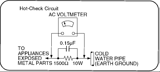
1.1.2. Leakage Current Hot Check (See
Figure 1.)
1.Plug the AC cord directly into the AC outlet. Do not use an
isolation transformer for this check.
2.Connect a 1.5k9, 10 watts resistor, in parallel with a 0.15µF
capacitors, between each exposed metallic part on the set
and a good earth ground such as a water pipe, as shown in
Figure 1.
3.Use an AC voltmeter, with 1000 ohms/volt or more
sensitivity, to measure the potential across the resistor.
4.Check each exposed metallic part, and measure the
voltage at each point.
5.Reverse the AC plug in the AC outlet and repeat each of the
above measurements.
6.The potential at any point should not exceed 0.75 volts
RMS. A leakage current tester (Simpson Model 229 or
equivalent) may be used to make the hot checks, leakage
current must not exceed 1/2 milliamp. In case a
measurement is outside of the limits specified, there is a
possibility of a shock hazard, and the equipment should be
repaired and rechecked before it is returned to the
customer.
4
Page 5

TX-15LT2M / TX-15LT2Q / TX-15LT2Z / TX-15LT2X / TX-15LT2T
2 Prevention of Electro Static Discharge (ESD) to
Electrostatically Sensitive (ES) Devices
Some semiconductor (solid state) devices can be damaged easily by static electricity. Such components commonly are called
Electrostatically Sensitive (ES) Devices. Examples of typical ES devices are integrated circuits and some field-effect transistors and
semiconductor "chip" components. The following techniques should be used to help reduce the incidence of component damage
caused by electro static discharge (ESD).
1.Immediately before handling any semiconductor component or semiconductor-equipped assembly, drain off any ESD on your
body by touching a known earth ground. Alternatively, obtain and wear a commercially available discharging ESD wrist strap,
which should be removed for potential shock reasons prior to applying power to the unit under test.
2.After removing an electrical assembly equipped with ES devices, place the assembly on a conductive surface such as alminum
foil, to prevent electrostatic charge buildup or exposure of the assembly.
3.Use only a grounded-tip soldering iron to solder or unsolder ES devices.
4.Use only an anti-static solder removal device. Some solder removal devices not classified as "anti-static (ESD protected)" can
generate electrical charge sufficient to damage ES devices.
5.Do not use freon-propelled chemicals. These can generate electrical charges sufficient to damage ES devices.
6.Do not remove a replacement ES device from its protective package until immediately before you are ready to install it. (Most
replacement ES devices are packaged with leads electrically shorted together by conductive foam, alminum foil or comparable
conductive material).
7.Immediately before removing the protective material from the leads of a replacement ES device, touch the protective material
to the chassis or circuit assembly into which the device will be installed.
Caution
Be sure no power is applied to the chassis or circuit, and observe all other safety precautions.
8.Minimize bodily motions when handling unpackaged replacement ES devices. (Otherwise hamless motion such as the brushing
together of your clothes fabric or the lifting of your foot from a carpeted floor can generate static electricity (ESD) sufficient to
damage an ES device).
5
Page 6

TX-15LT2M / TX-15LT2Q / TX-15LT2Z / TX-15LT2X / TX-15LT2T
3 About lead free solder (PbF)
Note: Lead is listed as (Pb) in the periodic table of elements.
In the information below, Pb will refer to Lead solder, and PbF will refer to Lead Free Solder.
The Lead Free Solder used in our manufacturing process and discussed below is (Sn+Ag+Cu).
That is Tin (Sn), Silver (Ag) and (Cu) although other types are available.
This model uses Pb Free solder in it’s manufacture due to environmental conservation issues. For service and repair work, we’d
suggest the use of Pb free solder as well, although Pb solder may be used.
PCBs manufactured using lead free solder will have the PbF within a leaf Symbol
Caution
·Pb free solder has a higher melting point than standard solder. Typically the melting point is 50 ~ 70 °F (30 ~ 40 °C) higher.
Please use a high temperature s oldering iron and set it to 700 ± 20 °F (370 ± 10 °C).
·Pb free solder will tend to splash when heated too high (about 1100 °F or 600 °C).
If you must use Pb solder, please completely remove all of the Pb free solder on the pins or solder area before applying Pb
solder. If this is not practical, be sure to heat the Pb free solder until it melts, before applying Pb solder.
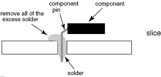
·After applying PbF solder to double layered boards, please check the component side for excess solder which may flow onto
the opposite side. (see figure below)
Suggested Pb free solder
There are several kinds of Pb free solder available for purchase. This product uses Sn+Ag+Cu (tin, silver, copper) solder.
However, Sn+Cu (tin, copper), Sn+Zn+Bi (tin, zinc, bismuth) solder can also be used.
stamped on the back of PCB.
6
Page 7
TX-15LT2M / TX-15LT2Q / TX-15LT2Z / TX-15LT2X / TX-15LT2T
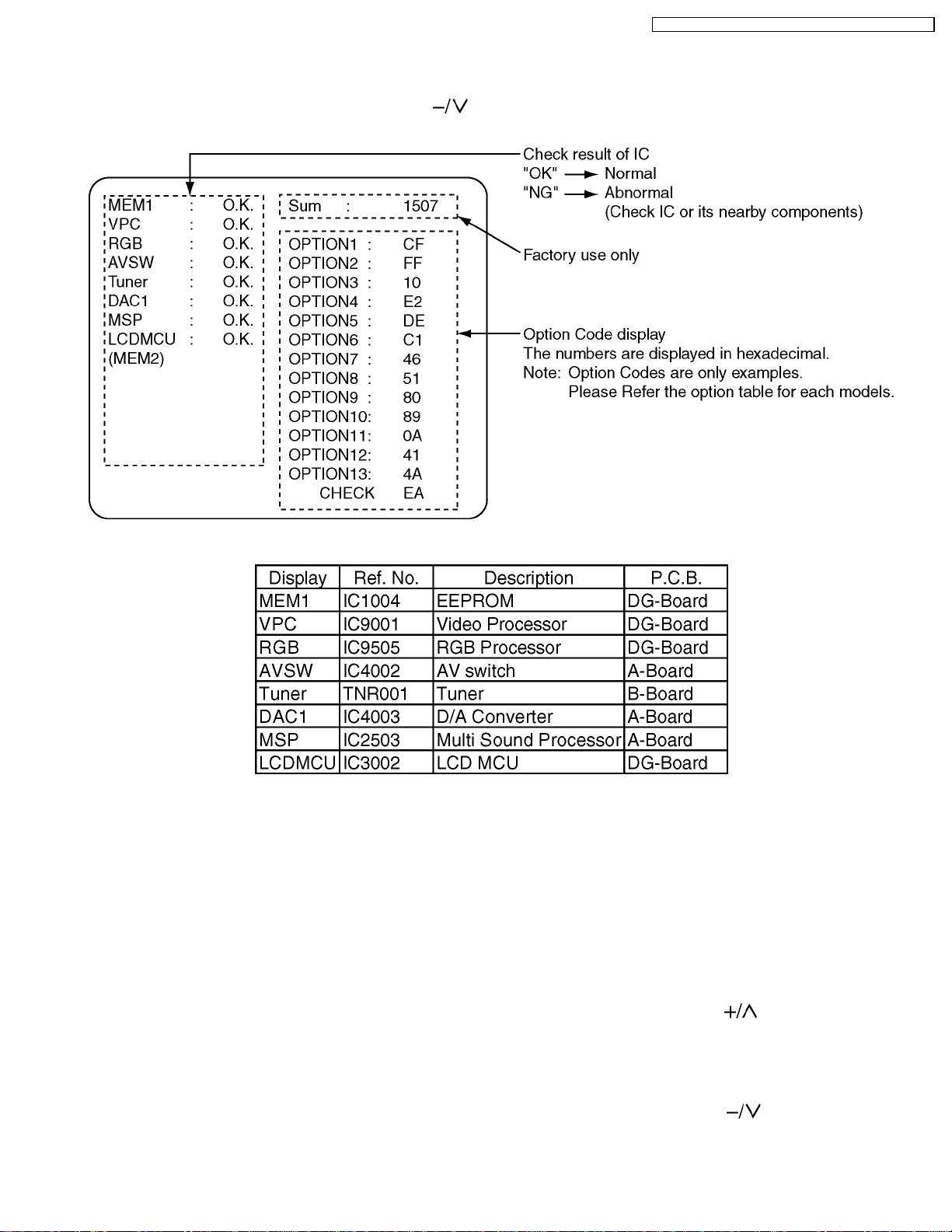
4SelfCheck
1.Self-Check is used to automatically check the bus lines and hexadecimal code of the TV set.
2.To get into the Self -Check mode press the [ Down (
time pressing the [ SET UP ] button on the remote control, and the screen will show :
) ] button on the customer controls at the front of the set, at the same
If the CCU ports have been checked and found to be incorrect or not located then “--” will appear in place of “O.K.”.
5 SERVICE HINTS
5.1. Hotel Mode
Purpose
1.At Hotels, this Mode prevent customer from changing the TV preset data, such as Channel preset data.
Note:
This Mode is useful for hotel, you should not get into “Hotel Mode” with Normal use.
Operation
1.To get into “ Hotel Mode”, press “Recall” button on the remote control and Channel up “[
simultaneously, after setting the “Off-Timer” mode.
2.In this mode, The Channel up and down Function will be able as normal Mode, and The maximum volume level for this
mode is set at the current volume level, that means setting at the level before entering the mode. However, other function
will be disable.
3.To exit This mode, press “SET UP” button on the remote control and the “Volume Down [
simultaneously.
* This Information is informed by Service Manual only.
]” key on the TV set
]” key on the TV set
7
Page 8
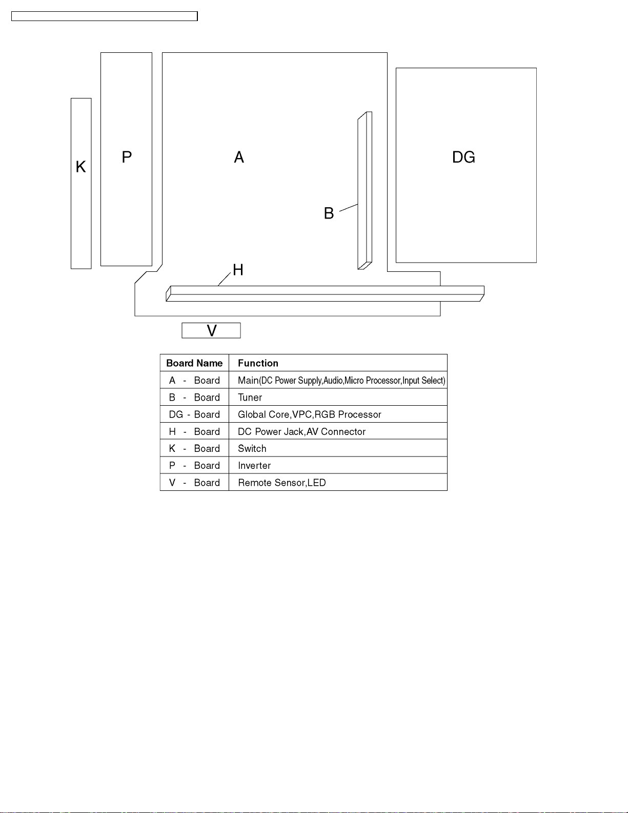
TX-15LT2M / TX-15LT2Q / TX-15LT2Z / TX-15LT2X / TX-15LT2T
6 Chasis Board Layout
8
Page 9
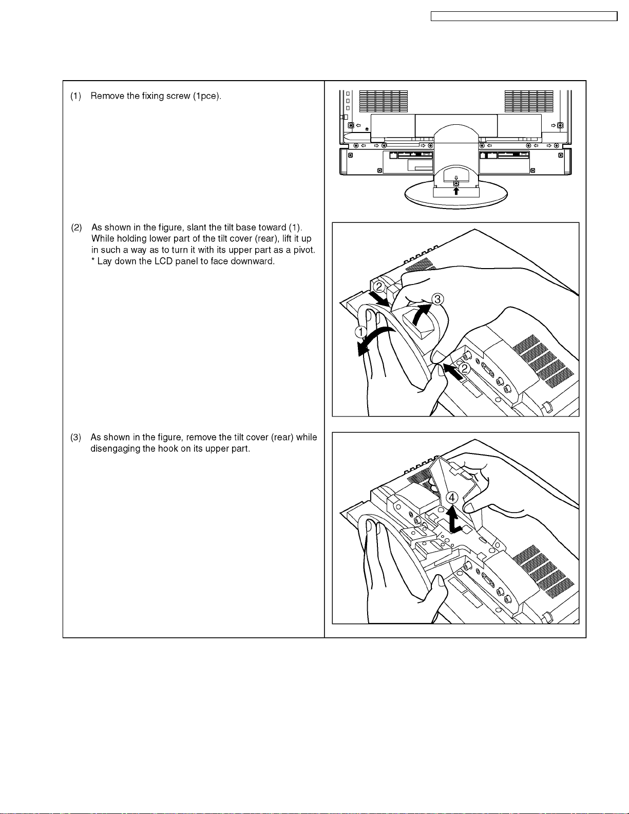
7 Servicing method
7.1. Removing tilt base
TX-15LT2M / TX-15LT2Q / TX-15LT2Z / TX-15LT2X / TX-15LT2T
9
Page 10
TX-15LT2M / TX-15LT2Q / TX-15LT2Z / TX-15LT2X / TX-15LT2T
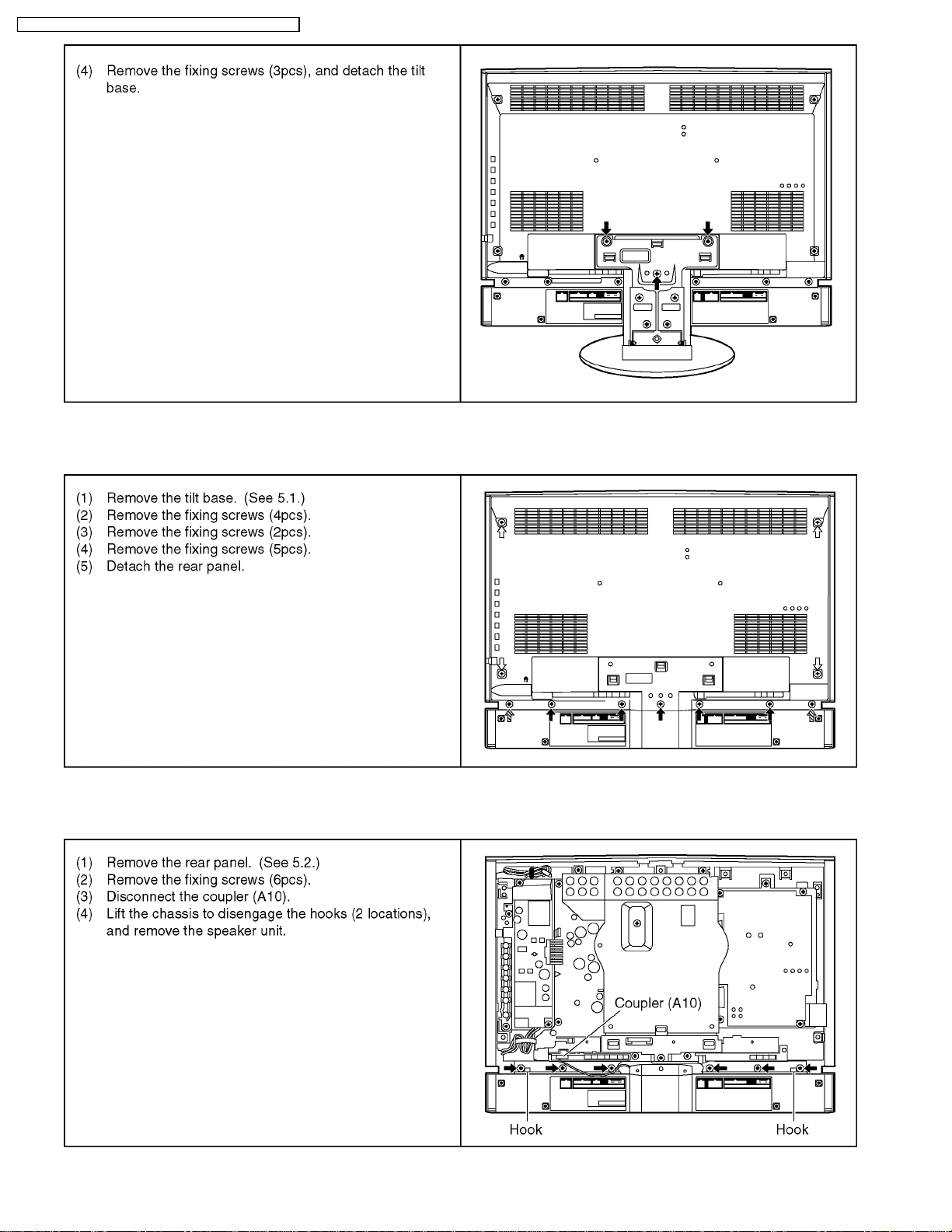
7.2. Removing rear panel
7.3. Removing speaker unit
10
Page 11
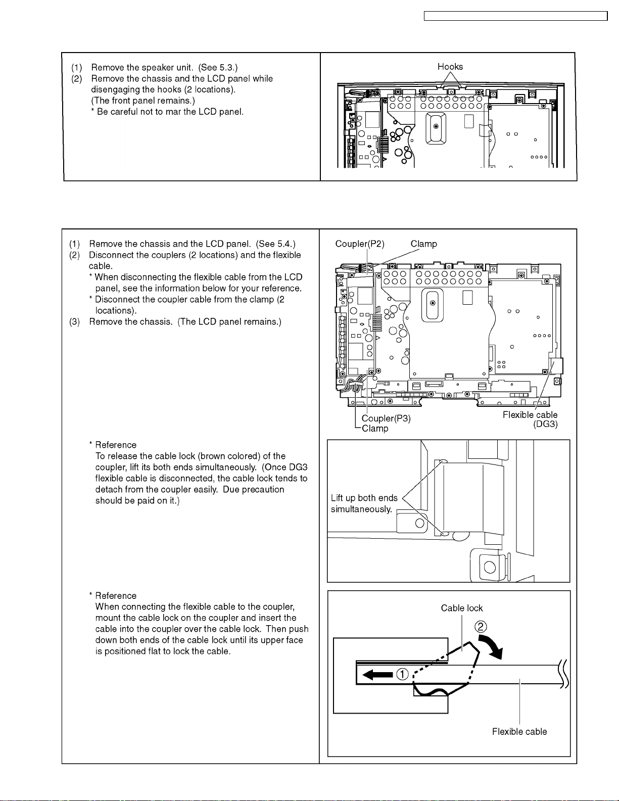
7.4. Removing front panel
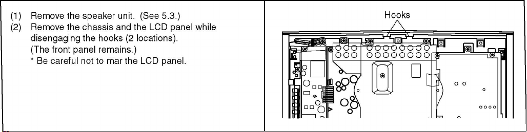
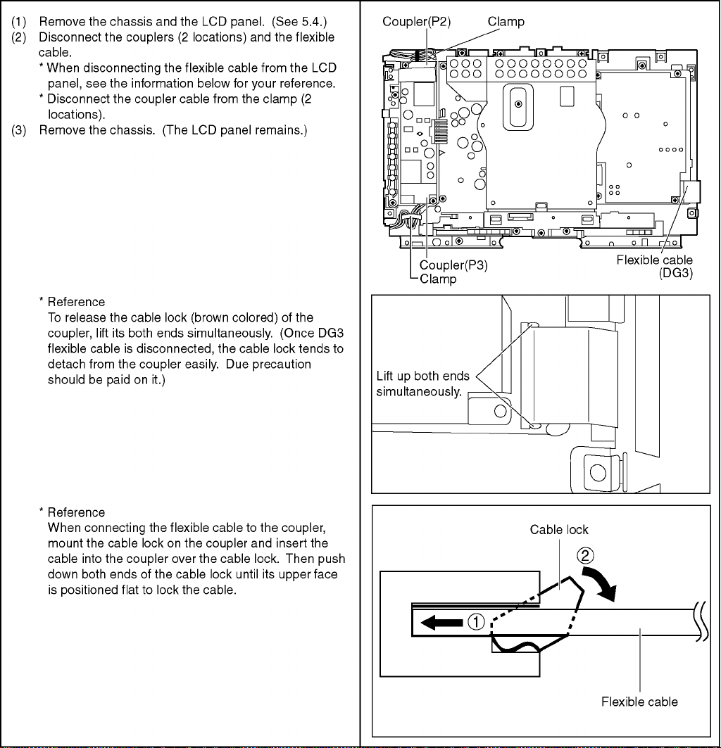
7.5. Removing LCD panel
TX-15LT2M / TX-15LT2Q / TX-15LT2Z / TX-15LT2X / TX-15LT2T
11
Page 12

TX-15LT2M / TX-15LT2Q / TX-15LT2Z / TX-15LT2X / TX-15LT2T
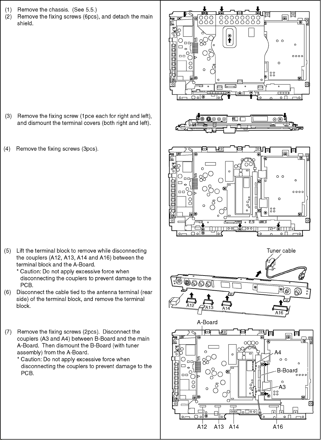
7.6. Removing main A-Board
12
Page 13
TX-15LT2M / TX-15LT2Q / TX-15LT2Z / TX-15LT2X / TX-15LT2T
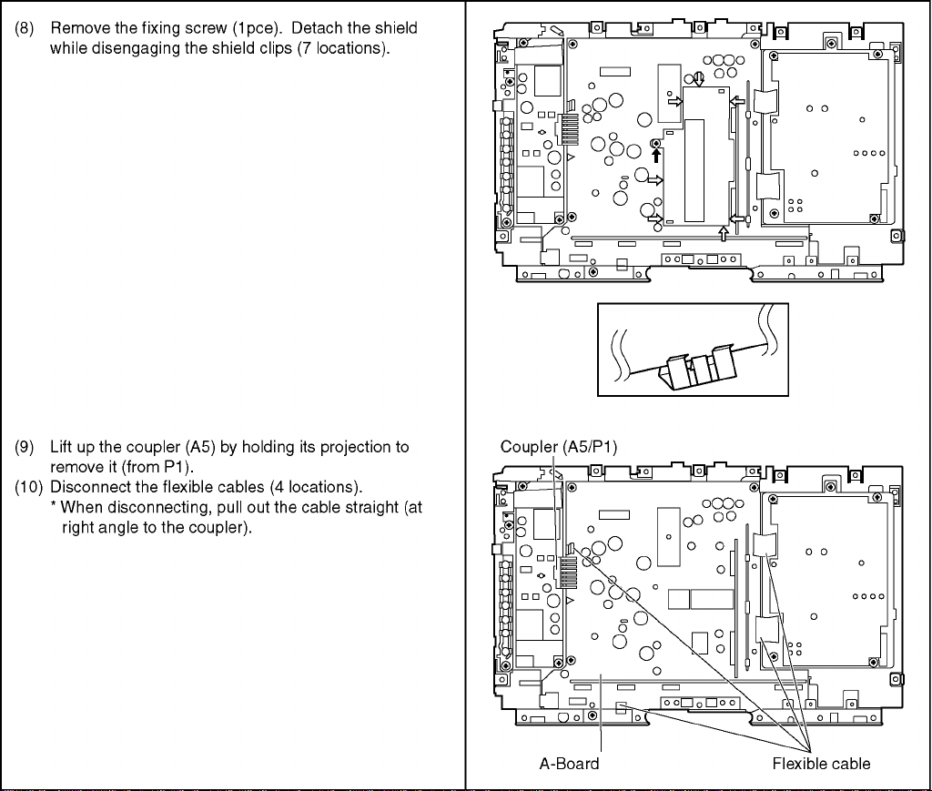
7.7. Removing B-Board (with tuner assembly)
13
Page 14

TX-15LT2M / TX-15LT2Q / TX-15LT2Z / TX-15LT2X / TX-15LT2T
7.8. Removing DG-Board
7.9. Removing H-Board
14
Page 15
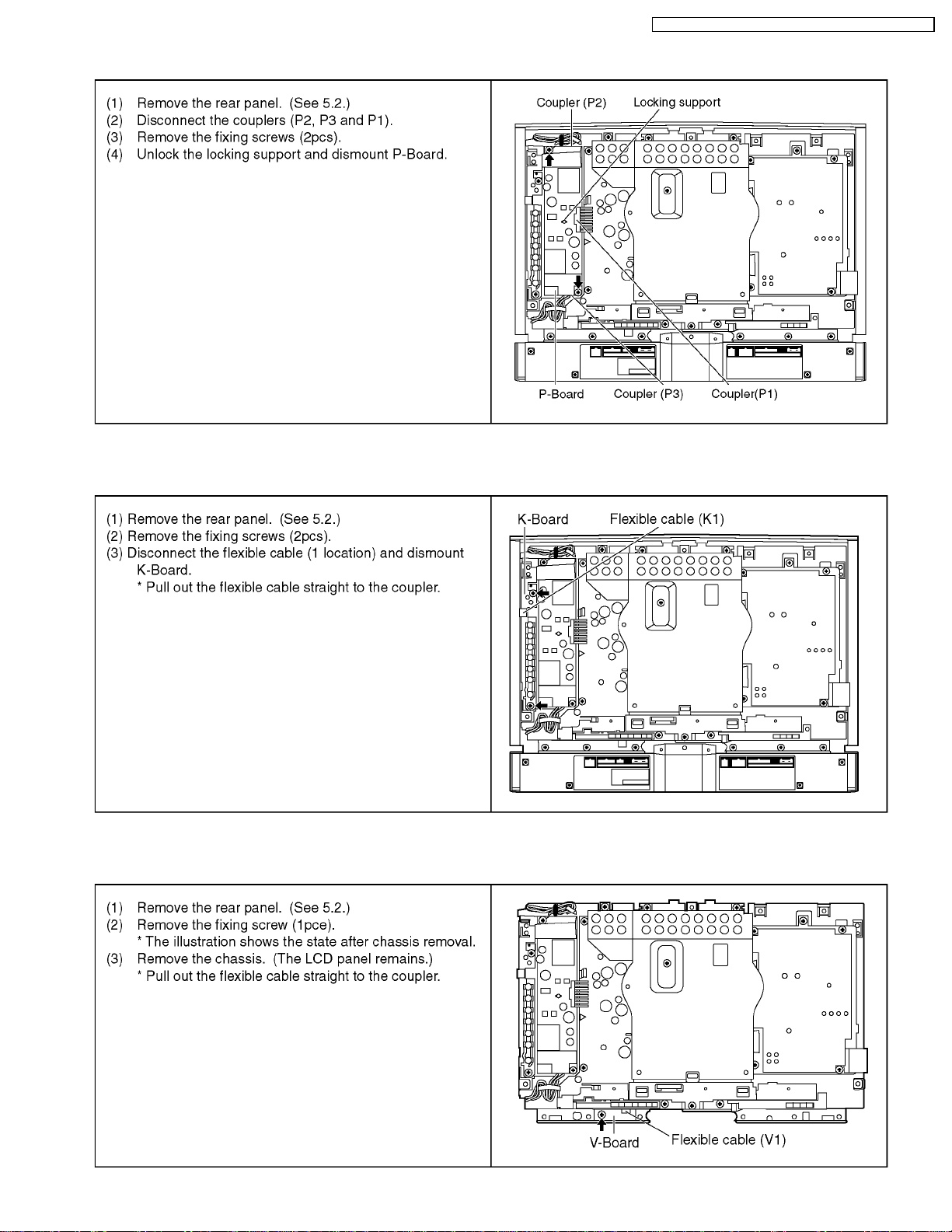
7.10. Removing P-Board
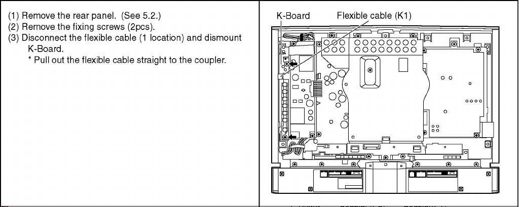
7.11. Removing K-Board
TX-15LT2M / TX-15LT2Q / TX-15LT2Z / TX-15LT2X / TX-15LT2T
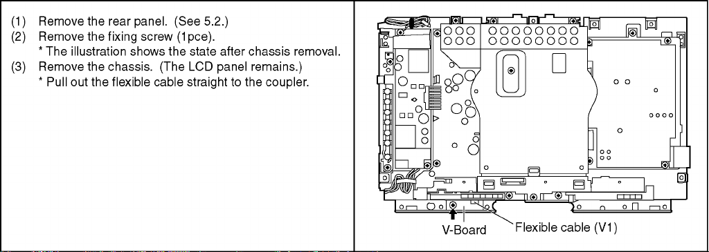
7.12. Pull out the flexible cable straight to the coupler.
15
Page 16
TX-15LT2M / TX-15LT2Q / TX-15LT2Z / TX-15LT2X / TX-15LT2T
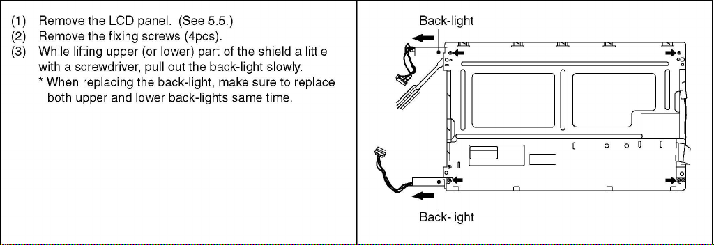
7.13. Removing back-light
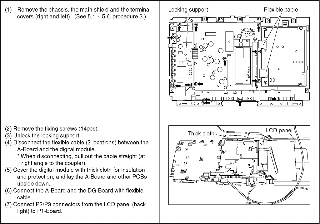
7.14. A-Board servicing
* Follow the procedures described below when checking voltage on rear side of the A-Board.
16
Page 17

TX-15LT2M / TX-15LT2Q / TX-15LT2Z / TX-15LT2X / TX-15LT2T
8 Service Mode Function
MPU controls the functions switching for each IICs through IIC bus in this chassis. The following setting and adjustment c an be
adjusted by remote control in Service Mode.
8.1. How to enter SERVICE 1
1.In sound menu, set BASS to MAXIMUM, and set TREBLE to MINIMUM.
2.Simultaneously press INDEX button on remote control and DOWN button [
8.2. How to enter SERVICE 2
1.Set the channel to CH99.
2.Press HOLD button on remote control.
Note:
To exit to Service mode, press N or Power button on remote control.
]ontheTVset.
17
Page 18
TX-15LT2M / TX-15LT2Q / TX-15LT2Z / TX-15LT2X / TX-15LT2T
18
Page 19
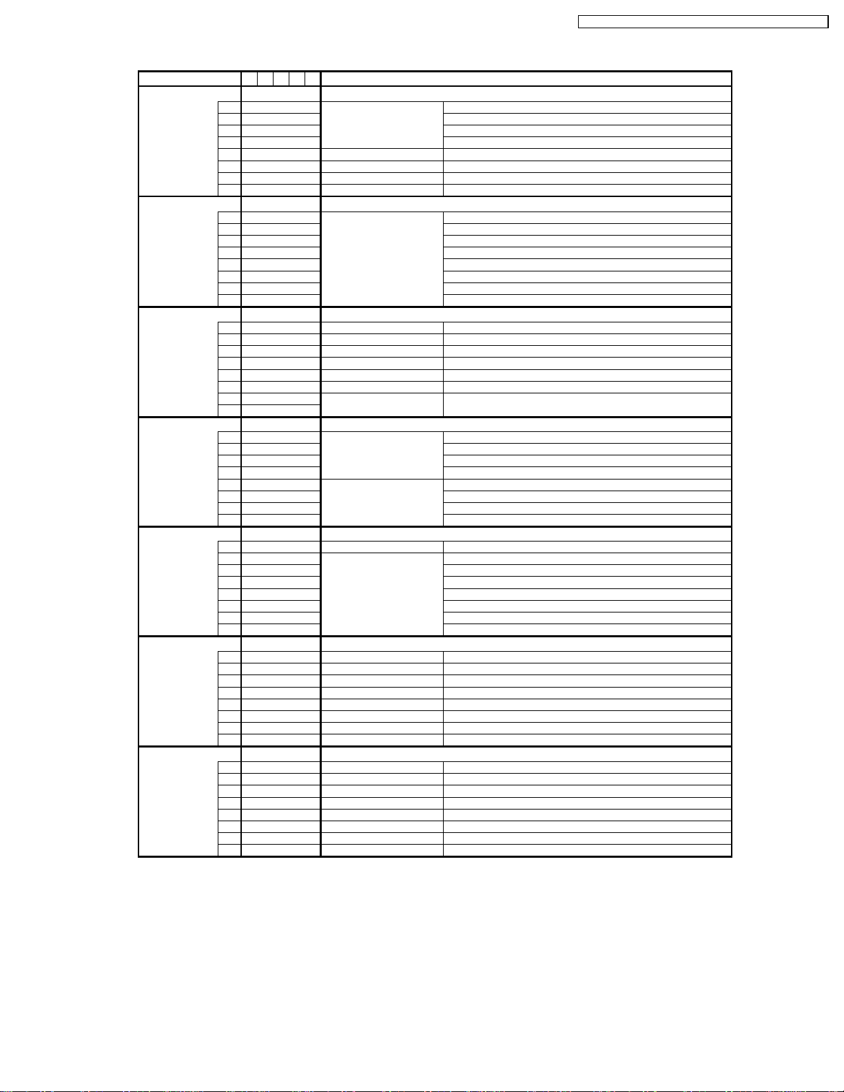
8.3. Option Description
ASIA / M.E. / HK / UK / CHINA (1)
AUSTRALIA (1)
E. EUROPE (1)
r
4.5 (1)
5.5 (1)
6.0 (1)
6.5 (1)
4.5 (1)
5.5 (1)
6.0 (1)
6.5 (1)
z
y
NZ / INDN (1)
AUSTRALIA (1)
E. EUROPE (1)
y
Auto(1)
NTSC(1)
not use
On (0), Off (1)
SASO enable (1)
set to 0
Q-Link on/off selectable in menu (1)
Display NICAM (0), Display MPX (1)
Description
TX-15LT2M / TX-15LT2Q / TX-15LT2Z / TX-15LT2X / TX-15LT2T
Option Models
option1
option2
option3
option4
option5
option6
option7
MQZ X T
b0 Colour system
b1
b2
b3
b4 TV NTSC 50
b5 TV SECAM 60
b6 AV NTSC 50
b7 AV SECAM 60
b0 CH Plan
b1 NZ / INDES (1)
b2
b3
b4 SPECIAL (1)
b5 AMERICA (1)
b6 CATV (1)
b7 JAPAN (1)
b0 sub picture
b1 2tune
b2 VGA
b3 YUV
b4 Wide (16:9)
b5 HYPER
b6 SIF I only(0), BG only(1)
b7 I/BG/DK/L(2), BG/DK(3)
b0 A2 enable
b1
b2
b3
b4 NICAM enable
b5
b6
b7
b0 A2 select 6.5MHz 5.742 MHz (0), 6.742 MH
b1 NICAM priorit
b2 HK / UK (1)
b3 CHINA (1)
b4
b5
b6
b7 SPECIAL (1)
b0 VCR/GAME in search
b1 SASO enable
b2 Noise mute
b3 Monitor out AV1 mute
b4 AV SW 3/2AV out
b5 Tuner
b6 Child lock Child lock enable (1)
b7 TEXT VDEFEAT VDEFEAT ON (1), OFF (0)
b0 Power up EC-Mode
b1 CH Blanking
b2 AV Blanking
b3 Auto WIDE
b4 Volume correction
b5 AVLink
b6 MPX/NICAM displa
b7 free
CF
FF
10
E2
DE
C1
46
1
1
1
1
0
0
1
1
1
1
1
1
1
1
1
1
0
0
0
0
1
0
0
0
0
1
0
0
0
1
1
1
0
1
1
1
1
0
1
1
1
0
0
0
0
0
1
1
0
1
1
0
0
0
1
0
SECAM(1)
M.NTSC(1)
Reserved
Reserved
Reserved
Reserved
without sub-picture (0), with sub-picture (1)
2 tuner (1), 1 tuner (0)
enable (1)
enable (1)
16:9 (1), 4:3 (0)
ASIA / M.E. (1)
Noise mute enable(0)
Monitor out AV1 mute(1)
MACO tuner (0), ALPS tuner (1)
Power on EC enable (1)
Blanking enable (1)
Blanking enable (1)
WSS enable only in aspect Auto (0), WSS always enable (1)
TV Volume correction enable (1)
19
Page 20
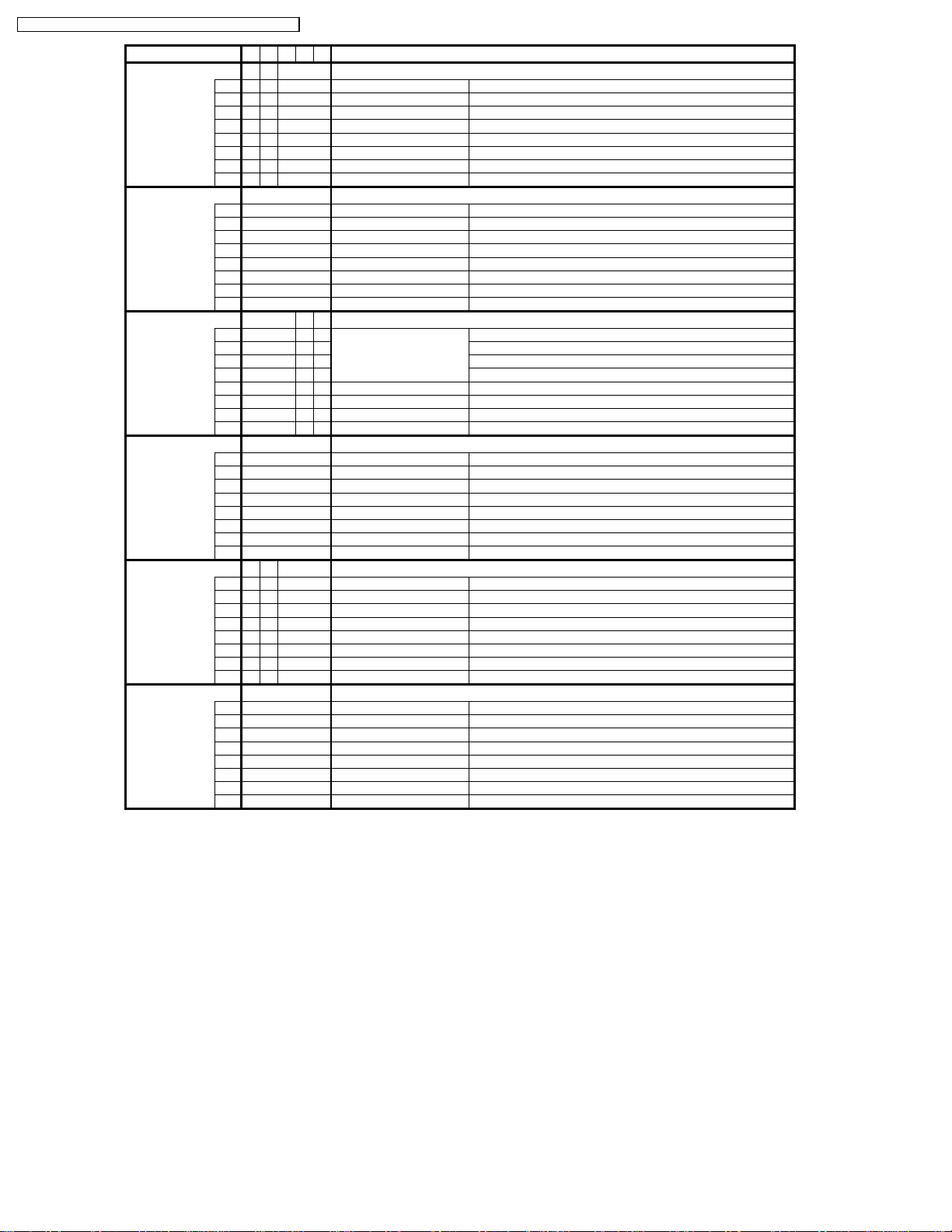
Description
r
y
y
y
y
A
(0),
)
(1)
(1)
option13
option12
option11
option10
TX-15LT2M / TX-15LT2Q / TX-15LT2Z / TX-15LT2X / TX-15LT2T
Option Models
option8
option9
MQZ X T
51 D0
b0 10 Teletext CH Refresh
00 Geomagnetic Senso
b1
b2 00 Geomagnetic Polarit
b3 00 RF Attenuation
11 Fine tuning
b4
00 Search speed
b5
11 TEXT FLOF
b6
b7
01 TEXT TOP
b0 free
b1 free
b2 free
b3 free
b4 free
b5 Surround SP polarit
b6 Volume curve
b7 Volume EXDAC
b0 1 1 OSD language English Only enable (1) : Top Prorit
b1 1 0
b2 0 1
b3 0 0
b4 0 0 Blue Back
b5 0 0 free
b6 0 0 free
b7 1 1 OVP
b0 Shop mode
b1 Full / 16:9 displa
b2 Sub Headphone
b3 Scan mode Blanking
b4 User aspect 14:9
b5 NICAM C4 bit
b6 ID-1
b7 1080i
41 43
11 Asia
b0
01 Australia Australia (1)
b1
00 Ireland Ireland(1)
b2
00 UK UK(1)
b3
00 MELCO
b4
00 28 inch
b5
11 Large size
b6
b7
00 PTV
b0 VDU Version
b1 GC Version
b2 UV Swap
b3 TEXT
b4 LT2 22inch
b5 free
b6 Picture Shift set to 1
b7 CIP2
89
51
1
0
0
0
1
0
1
0
Enable(1)
set to 0
set to 0
Enable(1)
Enable(1)
Slow(1) Fast(0)
Reserved
TOP enable
80
0
0
0
0
0
0
0
1
set to 0
Volume curve1(0), curve2(1)
Add Volume
83 85
1
0
0
1
0
Arabic enable (1)
Russian enable (1)
Chinese enable (1)
enable(0)
0
0
1
set to 1
0A
enable(1)
Reserved
enable (1)
Blanking enable (1)
enable (1)
enable (1)
enable (1)
enable
Asia (1), europe (0)
MELCOA (1)
Reserved for 28 inch etc.
set to 1
set to 0
A21 (0), A12(1)
ES5 (0), ES6 (1)
Swap (1)
Enable (1)
22inch (1), 15inch (0)
without CIP1
with CIP (1
4A
0
0
0
1
0
1
0
1
41
Area Option
1
0
0
0
0
0
1
0
Temporary
0
1
0
1
0
0
1
0
20
Page 21

TX-15LT2M / TX-15LT2Q / TX-15LT2Z / TX-15LT2X / TX-15LT2T
8.4. Option Code Setting
If the memory IC (IC1004) or DG Board is replaced, option code should be re-memorized.
Spare part of IC1004 is already memorized all Data for TX-15LT2M/Z.
If you use for other model, you should re-memorized the different option code in SERVICE 2 mode.
21
Page 22

TX-15LT2M / TX-15LT2Q / TX-15LT2Z / TX-15LT2X / TX-15LT2T
9 Adjustment
9.1. RF AGC Adjustment
1.Connect RF signal generator to antenna terminal.
2.Receive a RF signal, Colour bar.
3.Enter service 1 mode, and select RF AGC.
4.Adjustment begins when the blue button of the remote controller is pushed.
5.It waits to become stable.
6.The STR button of the remote controller is pushed, and adjustment value is saved.
9.2. DVCO Adjustment
1.Connect PAL colour bar signal generator to AV1 (SCART) terminal.
2.Input a PAL Color bar.
3.Enter service 1 mode, and select DVCO.
4.Adjustment begins when the blue button of the remote controller is pushed.
5.It waits to become stable.
6.The STR button on remote controller is pushed, and adjustment value is saved.
22
Page 23

Remarks:
1. The Power Circuit contains a circuit area which uses a separate power supply to isolate the
earth connection.
The circuit is defined by HOT and COLD indications in the schematic diagram. Take the
follwing precautions.
All circuits, except the Power Circuit, are cold.
Precautions
a. Do not touch the hot part or the hot and cold parts at the same time or you may
be shocked.
b. Do not short- circuit the hot and cold circuits or a fuse may blow and parts may
break.
c. Do not connect an instrument, such as an oscilloscope, to the hot and cold
circuits simultaneously or a fuse may blow.
Connect the earth of instruments to the earth connection of the circuit being
measured.
d. Make sure to disconnect the power plug before removing the chassis.
2. Following diodes are interchangeable.
MA150- MA162 (Replacement part)
TX-15LT2M/Q/T/X/Z
Schematic Diagram Notes
Page 24
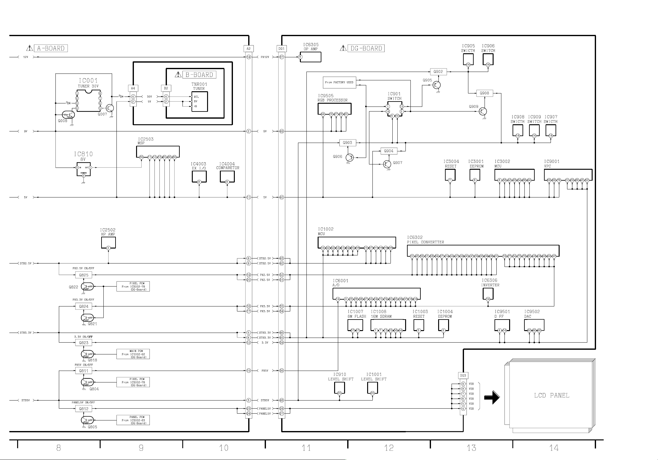
TX-15LT2M/Q/T/X/Z Power Block Diagram TX-15LT2M/Q/T/X/Z Power Block Diagram
Page 25
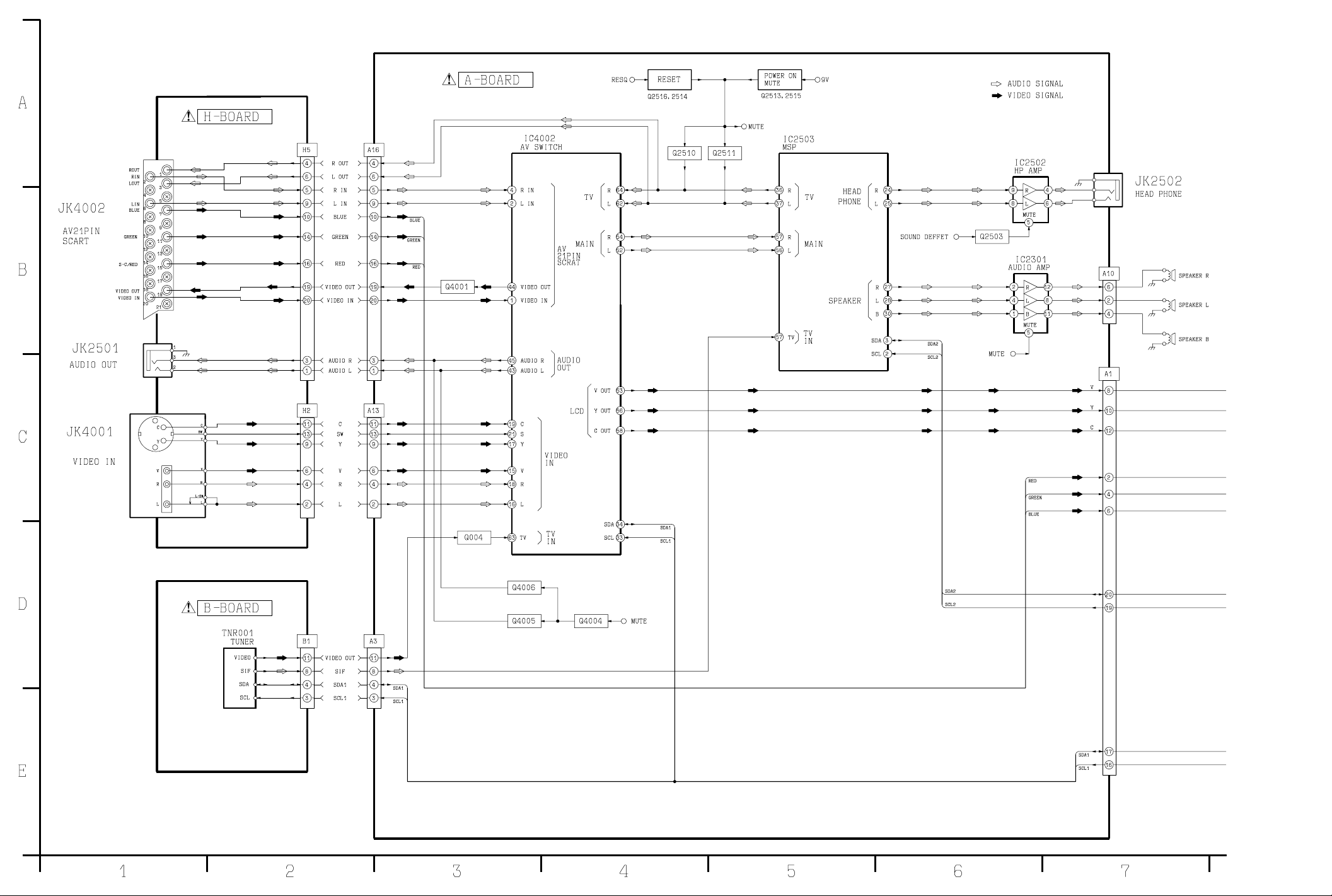
TX-15LT2M/Q/T/X/Z Signal Block Diagram TX-15LT2M/Q/T/X/Z Signal Block Diagram
Page 26
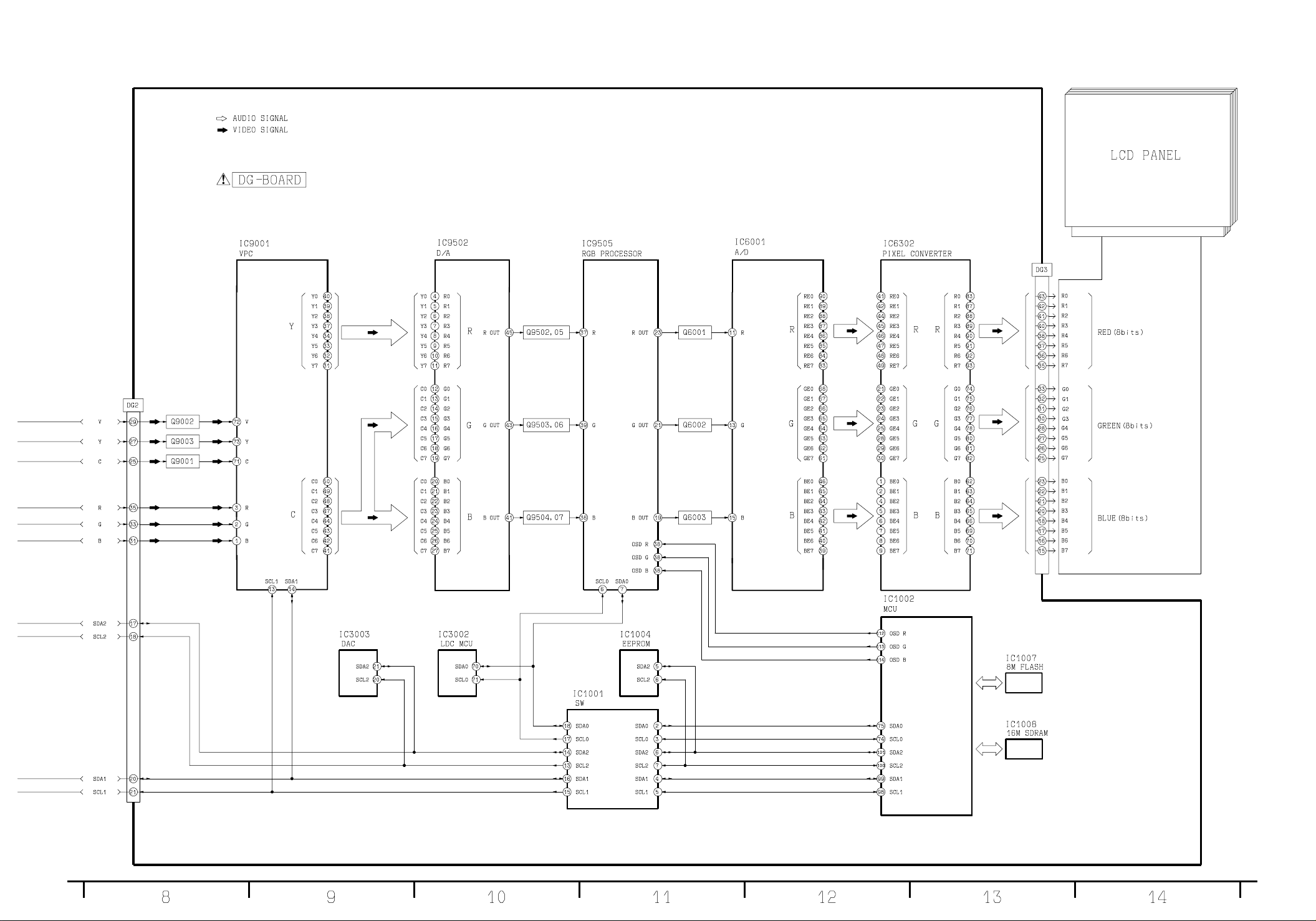
TX-15LT2M/Q/T/X/Z Signal Block Diagram TX-15LT2M/Q/T/X/Z Signal Block Diagram
Page 27
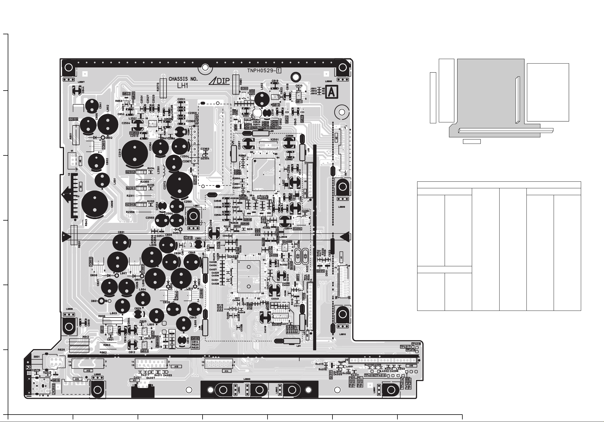
A-BOARD (COMPONENT SIDE)
6
5
4
3
2
TNPH0529
Parts Location
IC
IC001 D-6
IC801 B-5
IC802 C-3
IC803 B-3
IC804 C-2
IC806 B-5
IC808 C-2
IC810 C-3
IC2301 C-5
IC2502 B-5
IC2503 D-4
IC4001 E-2
IC4002 D-3
IC4003 E-3
IC4004 E-3
TRANSISTOR
Q001 E-3
Q003 E-2
Q004 D-3
Q005 E-3
Q802 C-2
Q803 C-2
Q806 C-2
Q808 C-2
A
A-BOARD (COMPONENT SIDE)
Q810 B-2
Q811 E-5
Q812 E-5
Q816 A-1
Q822 B-5
Q823 E-5
Q824 E-5
Q825 B-5
Q826 D-5
Q2301 B-4
Q2302 B-4
Q2303 B-4
Q2504 D-4
Q2505 D-4
Q2506 D-3
Q2510 E-5
Q2511 E-5
Q2512 C-4
Q2517 D-5
Q2518 D-5
Q4001 E-1
Q4002 E-3
Q4003 E-3
Q4004 E-3
Q4005 D-3
Q4006 E-3
TP
TP4010 F-1
TP4011 F-1
TP4012 F-1
TP4013 F-1
TP4014 G-1
TP4015 F-1
TP4016 F-1
TP4017 G-2
TP4018 G-2
TP4019 G-2
TP4207 G-1
TP4209 G-1
1
TX-15LT2M/Q/T/X/Z
A-BOARD TNPA0529
A
TX-15LT2M/Q/T/X/Z
A-BOARD TNPA0529
C EGBDF
Page 28

A-BOARD (FOIL SIDE)
6
5
4
3
2
TNPH0529
Parts Location
IC
IC2301 D-4
TRANSISTOR
Q002 B-3
Q007 C-5
Q008 C-5
Q801 E-2
Q804 C-6
Q805 C-6
Q807 E-2
Q809 E-2
Q813 E-2
Q814 E-2
Q815 E-2
Q817 F-4
Q818 C-5
Q819 F-4
Q820 F-5
Q821 C-5
Q2301 E-4
Q2302 E-4
Q2303 E-4
Q2501 E-5
Q2502 E-5
Q2503 E-5
Q2513 E-4
Q2514 D-4
Q2515 E-4
A
A-BOARD (FOIL SIDE)
TP
Q2516 D-4
Q2519 E-5
TP801 B-5
TP802 F-5
TP803 F-6
TP804 B-2
TP805 F-1
TP806 F-5
TP807 E-2
TP808 E-2
TP809 E-3
TP810 F-3
TP811 F-4
TP812 E-2
TP813 D-2
TP814 E-3
TP815 E-3
TP816 E-3
TP817 E-2
TP818 D-2
TP819 D-3
TP820 F-4
TP844 F-1
TP2323 D-5
TP2324 D-5
TP2331 E-4
TP2332 E-4
TP2333 D-5
TP2334 D-5
TP2336 E-4
TP2337 E-4
TP4020 D-3
TP4021 D-3
TP4022 C-2
TP4023 C-2
TP4024 B-1
TP4025 B-1
TP4028 C-3
TP4029 C-3
1
TX-15LT2M/Q/T/X/Z
A-BOARD TNPA0529
A
TX-15LT2M/Q/T/X/Z
A-BOARD TNPA0529
C EGBDF
Page 29
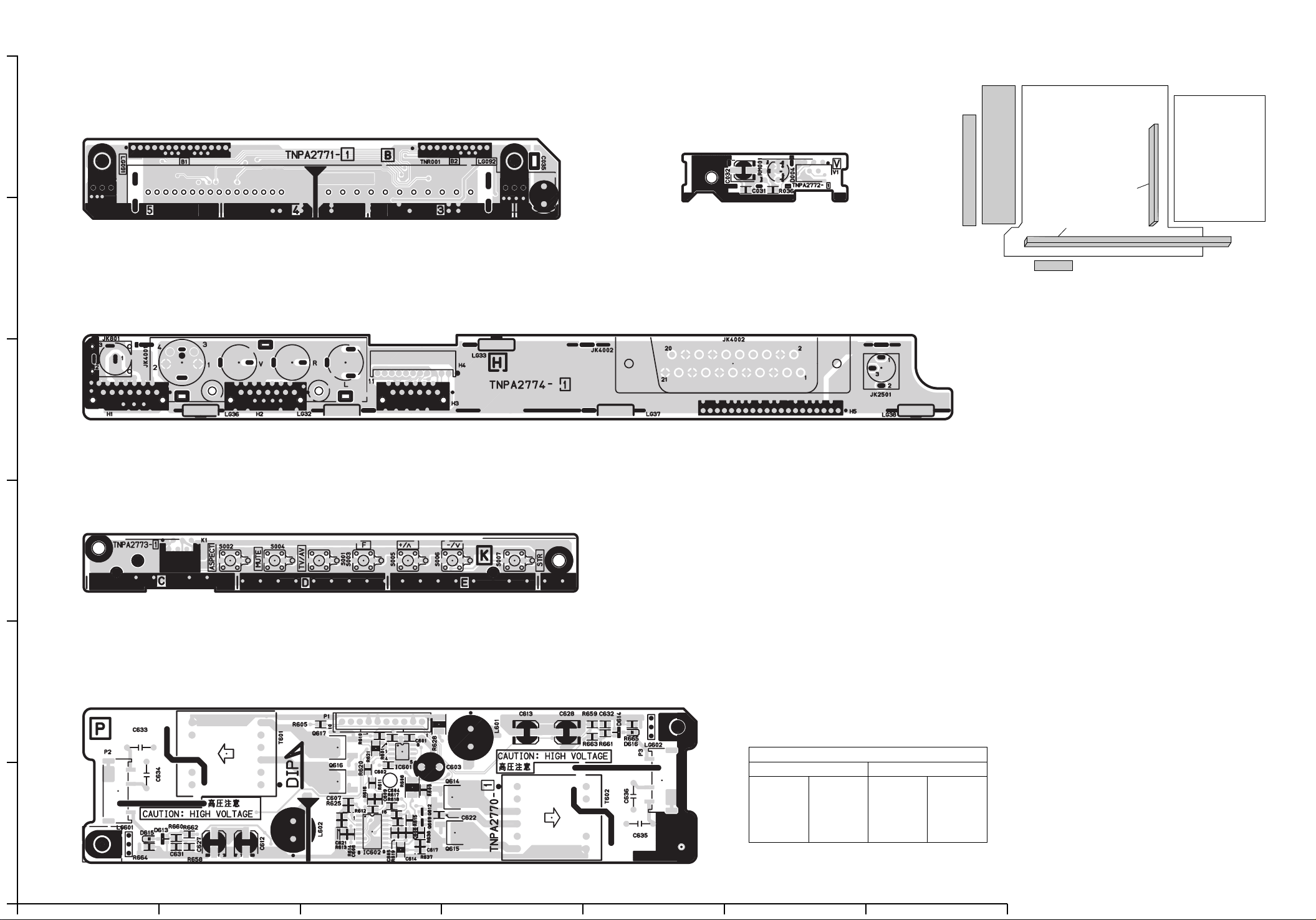
B-BOARD (COMPONENT SIDE)
6
TXN/B10HGK
V-BOARD (COMPONENT SIDE)
TNPA2772
P
K
B
H
5
V
H-BOARD (COMPONENT SIDE)
TNPA2774
4
K-BOARD (COMPONENT SIDE)
TNPA2773
3
P-BOARD (COMPONENT SIDE)
2
1
TX-15LT2M/Q/T/X/Z
B-BOARD TXN/B10HGK H-BOARD TNPA2774 K-BOARD TNPA2773
P-BOARD TNPA2770 V-BOARD TNPA2772
TNPA2770
A
Parts Location
P-BOARD (COMPONENT SIDE)
IC
IC601 C-2
IC602 C-1
TRANSISTOR
Q609 C-1
Q612 C-1
Q614 D-1
Q615 D-1
Q616 C-2
Q617 C-2
TX-15LT2M/Q/T/X/Z
B-BOARD TXN/B10HGK H-BOARD TNPA2774 K-BOARD TNPA2773
P-BOARD TNPA2770 V-BOARD TNPA2772
C EGBDF
Page 30
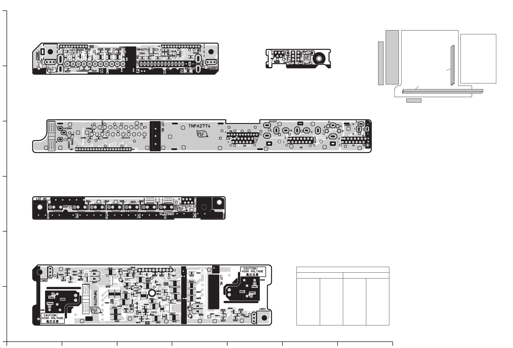
B-BOARD (FOIL SIDE)
6
TXN/B10HGK
V-BOARD (FOIL SIDE)
TNPA2772
P
K
B
H
5
H-BOARD (FOIL SIDE)
V
TNPA2774
4
K-BOARD (FOIL SIDE)
TNPA2773
3
P-BOARD (FOIL SIDE)
2
1
TX-15LT2M/Q/T/X/Z
B-BOARD TXN/B10HGK H-BOARD TNPA2774 K-BOARD TNPA2773
P-BOARD TNPA2770 V-BOARD TNPA2772
TNPA2770
A
Parts Location
P-BOARD (FOIL SIDE)
TRANSISTOR
Q601 C-2
Q602 C-2
Q603 C-2
Q604 C-2
Q605 C-1
Q606 B-2
Q607 C-1
Q608 E-1
Q610 C-1
Q611 B-2
Q613 C-1
TP
TP601 E-2
TP602 E-1
TP603 A-1
TP604 A-1
TP605 E-1
TP606 A-2
TX-15LT2M/Q/T/X/Z
B-BOARD TXN/B10HGK H-BOARD TNPA2774 K-BOARD TNPA2773
P-BOARD TNPA2770 V-BOARD TNPA2772
C EGBDF
Page 31
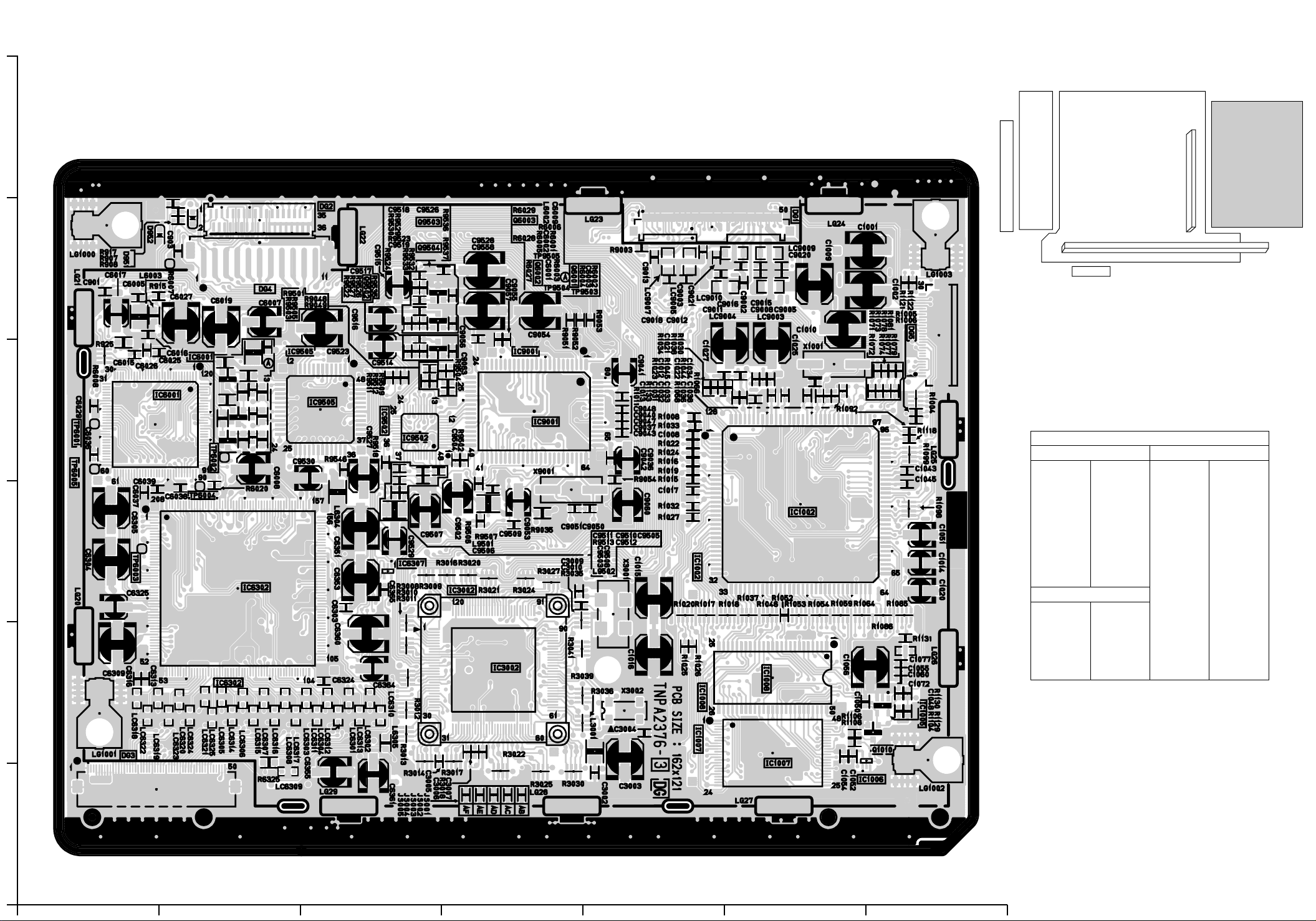
DG-BOARD (COMPONENT SIDE)
6
5
4
3
2
TXNDG10HGK
Parts Location
DG-BOARD (COMPONENT SIDE)
IC
IC1002 E-3
IC1005 G-2
IC1006 G-1
IC1007 E-2
IC1008 E-2
IC3002 D-3
IC6001 B-4
IC6302 B-2
IC6307 C-3
IC9001 D-4
IC9502 C-4
IC9505 C-4
TRANSISTOR
Q1010 G-2
Q6001 D-5
Q6002 D-5
Q6003 D-5
Q9502 C-5
Q9503 C-5
Q9504 C-5
TP
TP6001 A-4
TP6002 B-4
TP6003 A-3
TP6004 B-3
TP6005 A-4
TP9503 E-5
TP9504 D-5
TP9505 D-5
DG
1
TX-15LT2M/Q/T/X/Z
DG-BOARD TXNDG10HGK
A
TX-15LT2M/Q/T/X/Z
DG-BOARD TXNDG10HGK
C EGBDF
Page 32
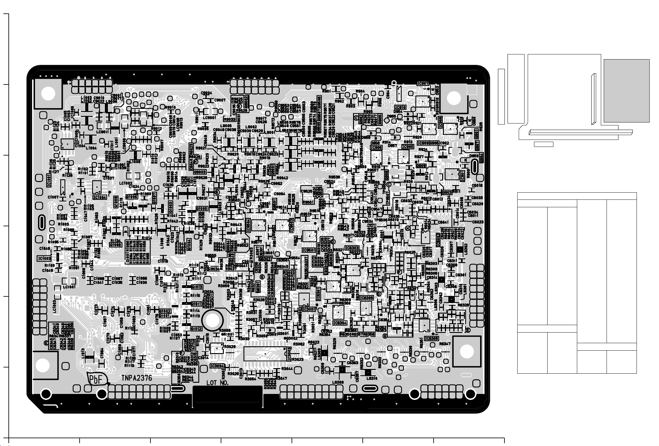
DG-BOARD (FOIL SIDE)
6
5
TXNDG10HGK
DG
4
Parts Location
DG-BOARD (FOIL SIDE)
IC
IC901 G-4
IC905 F-5
IC906 F-5
IC907 F-6
IC908 G-5
IC909 F-5
IC910 F-5
IC1001 A-4
IC1003 A-3
3
2
IC1004 B-4
IC1009 A-5
IC3001 E-2
IC3003 D-2
IC3004 C-2
IC6002 G-3
IC6301 E-3
IC6303 E-3
IC6304 E-2
IC6305 F-2
IC6306 F-2
IC9501 E-3
IC9503 D-4
IC9504 D-4
TRANSISTOR
Q901 G-5
Q902 E-5
Q903 G-4
Q904 G-4
Q905 F-5
Q906 F-5
Q907 G-5
Q908 F-4
Q909 F-4
Q1001 C-2
Q1002 C-2
Q1003 C-4
Q1004 C-3
Q1005 C-4
Q1006 B-4
Q1007 C-4
Q1008 B-3
Q1009 B-4
Q1011 C-2
Q1012 C-2
Q1013 C-3
Q3001 D-2
Q3002 D-2
Q6301 D-3
Q6302 D-3
Q6303 E-3
Q6304 C-1
Q9001 D-4
Q9002 D-5
Q9003 C-4
Q9004 D-3
Q9501 D-4
Q9505 E-5
Q9506 E-5
Q9507 E-5
TP
TP9058 F-4
TP9506 F-4
TP9507 F-4
1
TX-15LT2M/Q/T/X/Z
DG-BOARD TXNDG10HGK
A
TX-15LT2M/Q/T/X/Z
DG-BOARD TXNDG10HGK
C EGBDF
Page 33
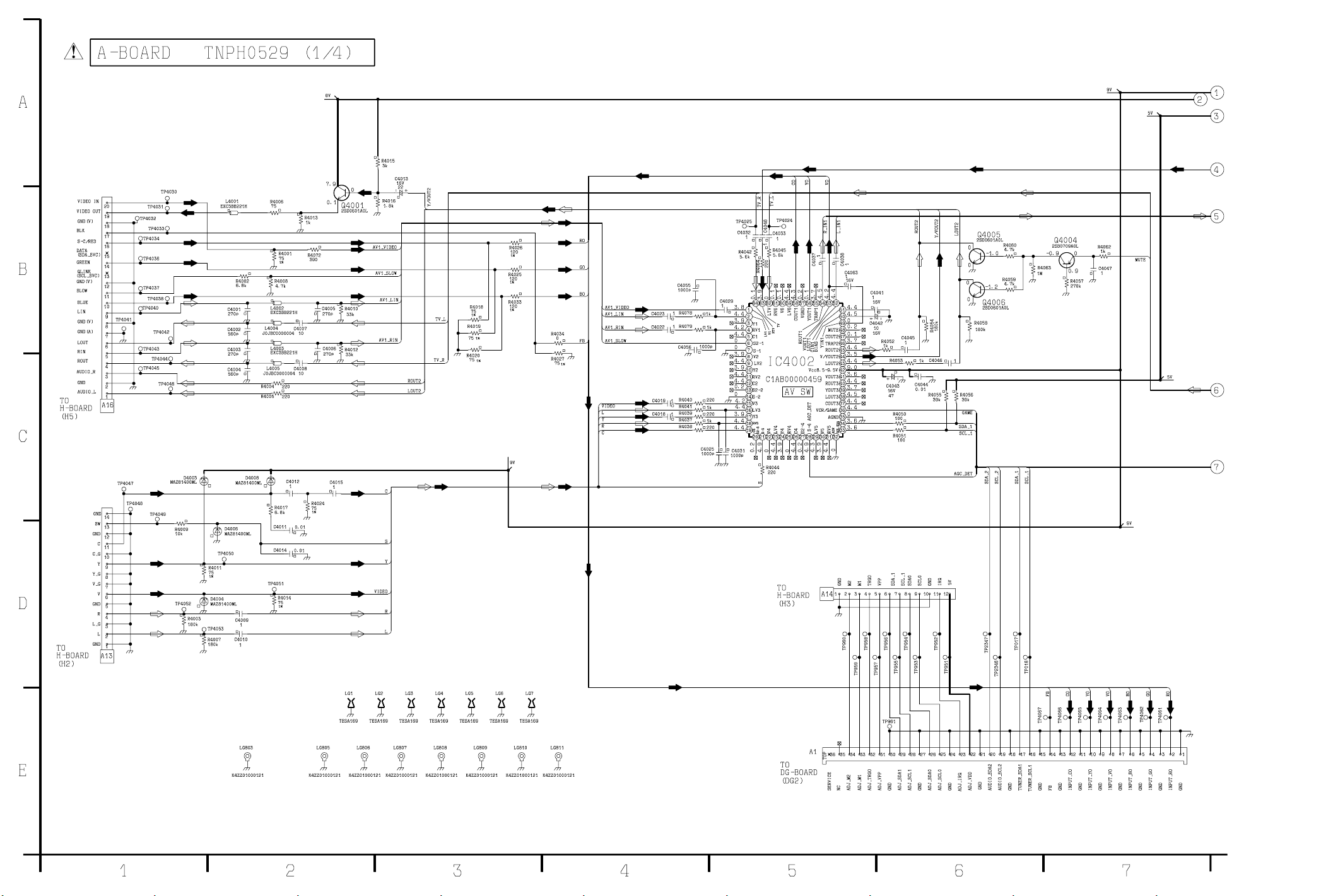
TX-15LT2M/Q/T/X/Z
A-Board (1 of 4) Schematic Diagram
TX-15LT2M/Q/T/X/Z
A-Board (1 of 4) Schematic Diagram
Page 34
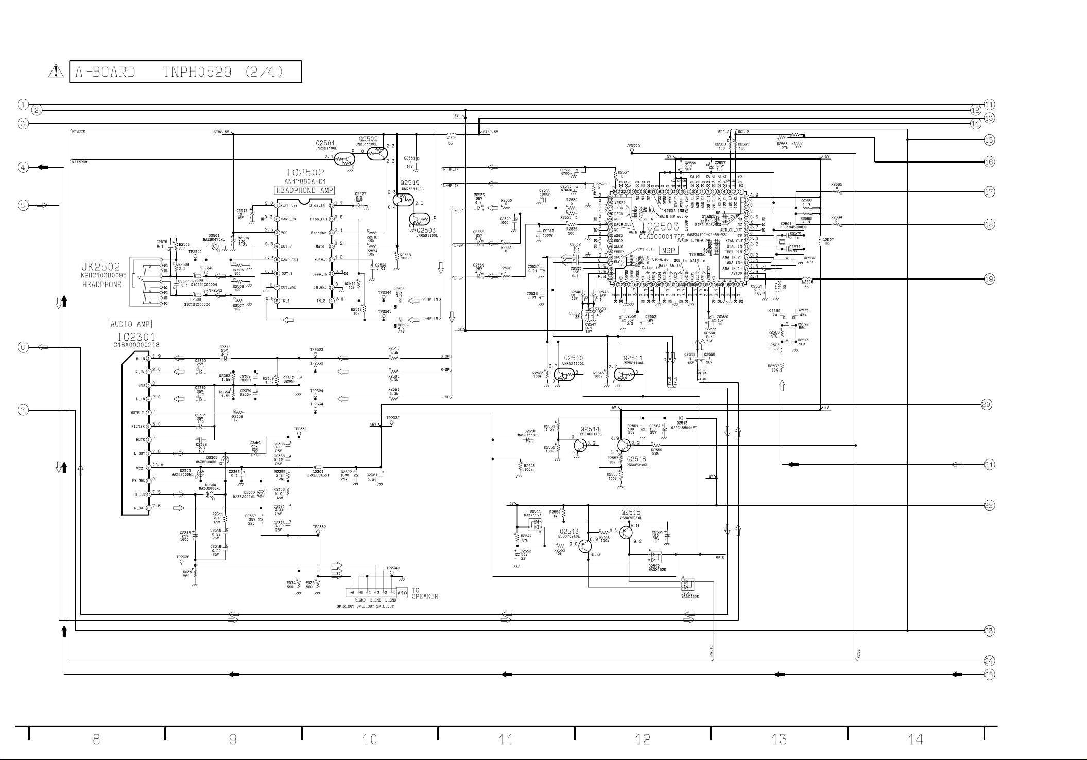
TX-15LT2M/Q/T/X/Z
A-Board (2 of 4) Schematic Diagram
TX-15LT2M/Q/T/X/Z
A-Board (2 of 4) Schematic Diagram
Page 35
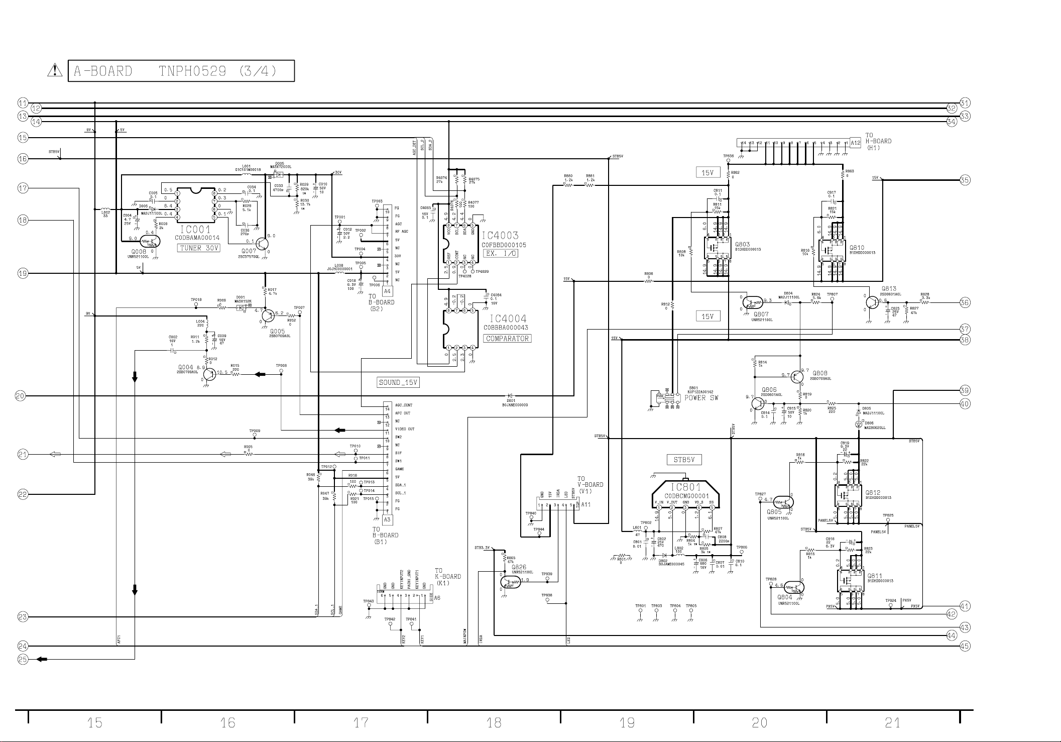
TX-15LT2M/Q/T/X/Z
A-Board (3 of 4) Schematic Diagram
TX-15LT2M/Q/T/X/Z
A-Board (3 of 4) Schematic Diagram
Page 36
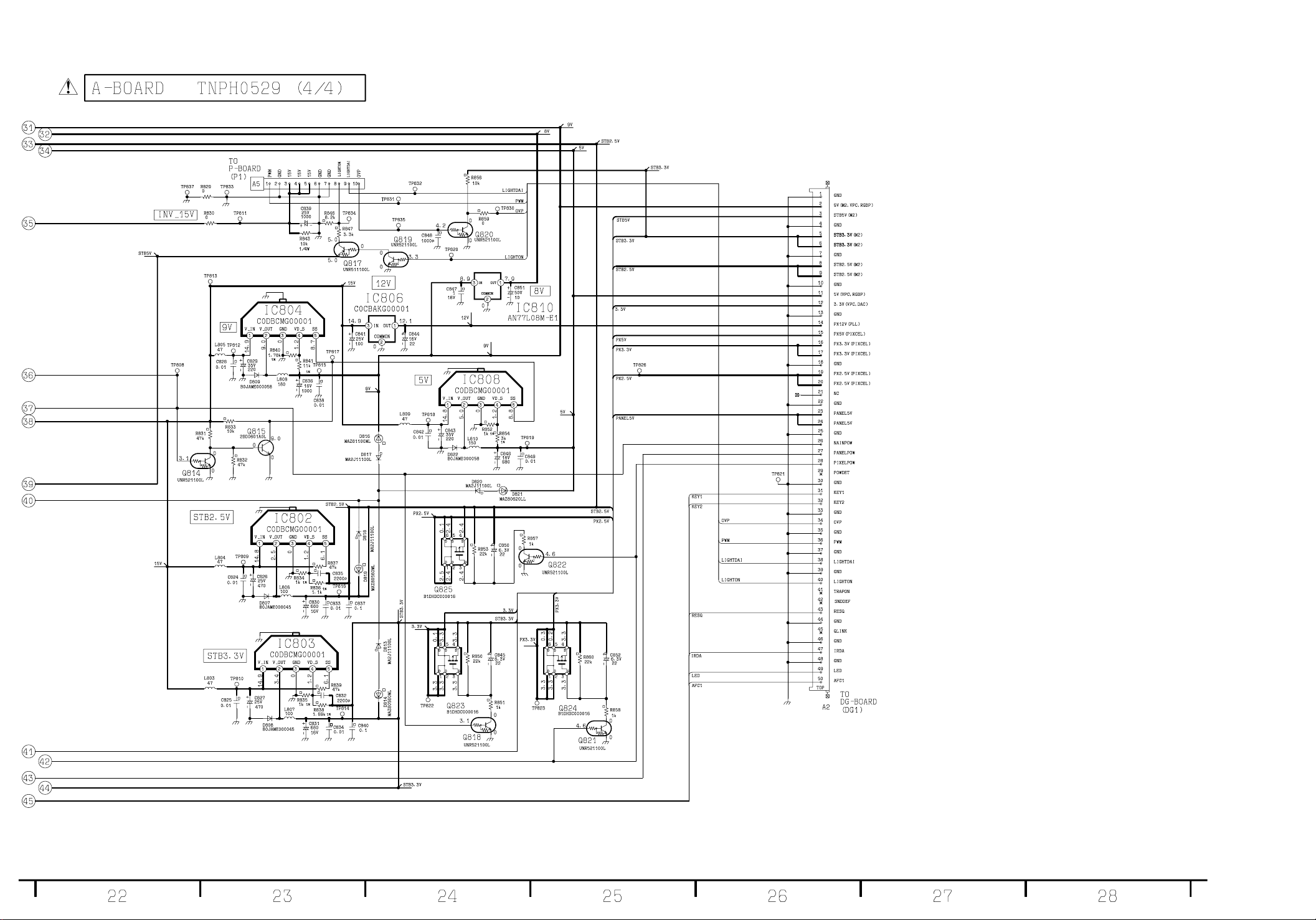
TX-15LT2M/Q/T/X/Z
A-Board (4 of 4) Schematic Diagram
TX-15LT2M/Q/T/X/Z
A-Board (4 of 4) Schematic Diagram
Page 37
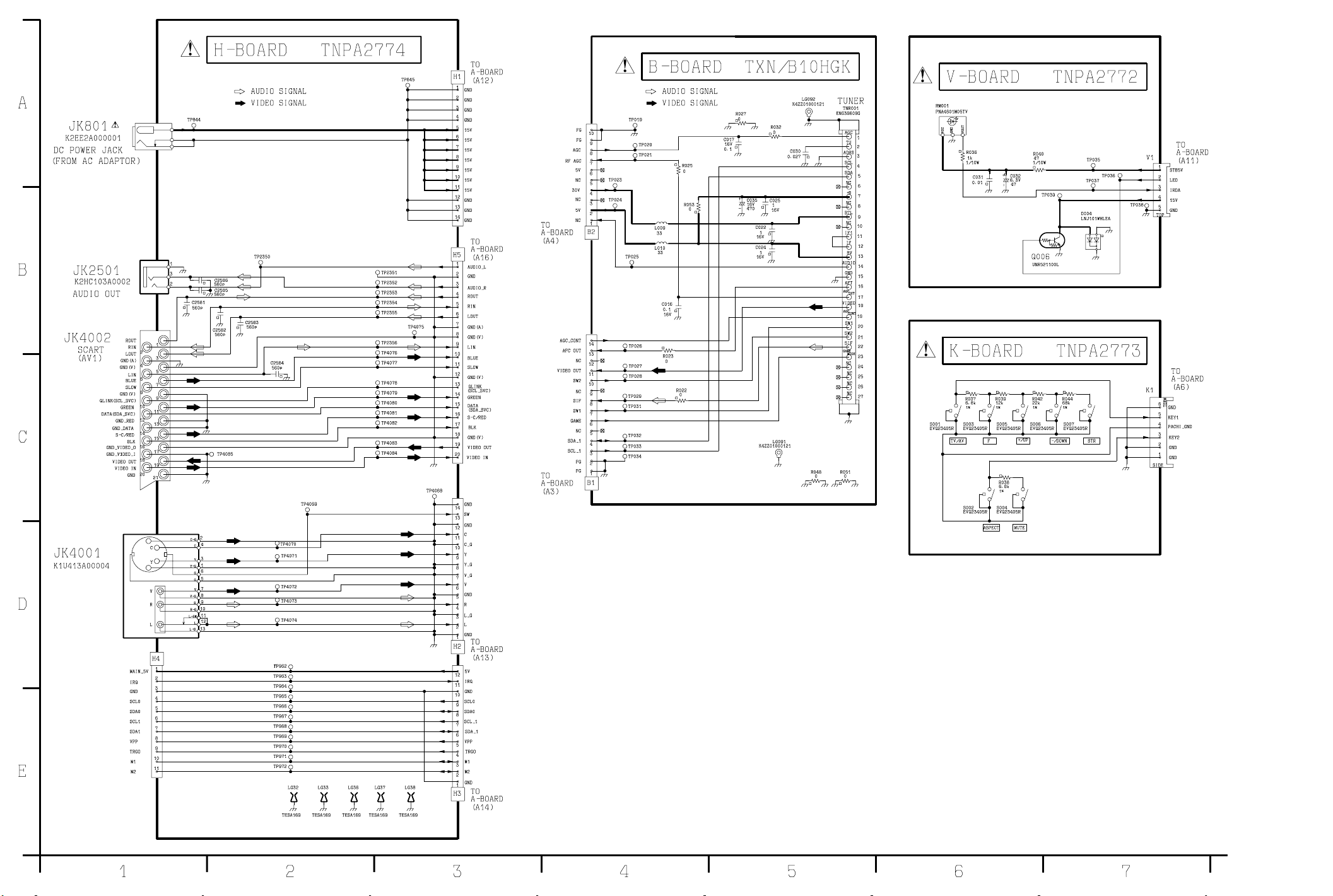
TX-15LT2M/Q/T/X/Z B,H,K,and V-Board Schematic Diagram TX-15LT2M/Q/T/X/Z B,H,K,and V-Board Schematic Diagram
Page 38
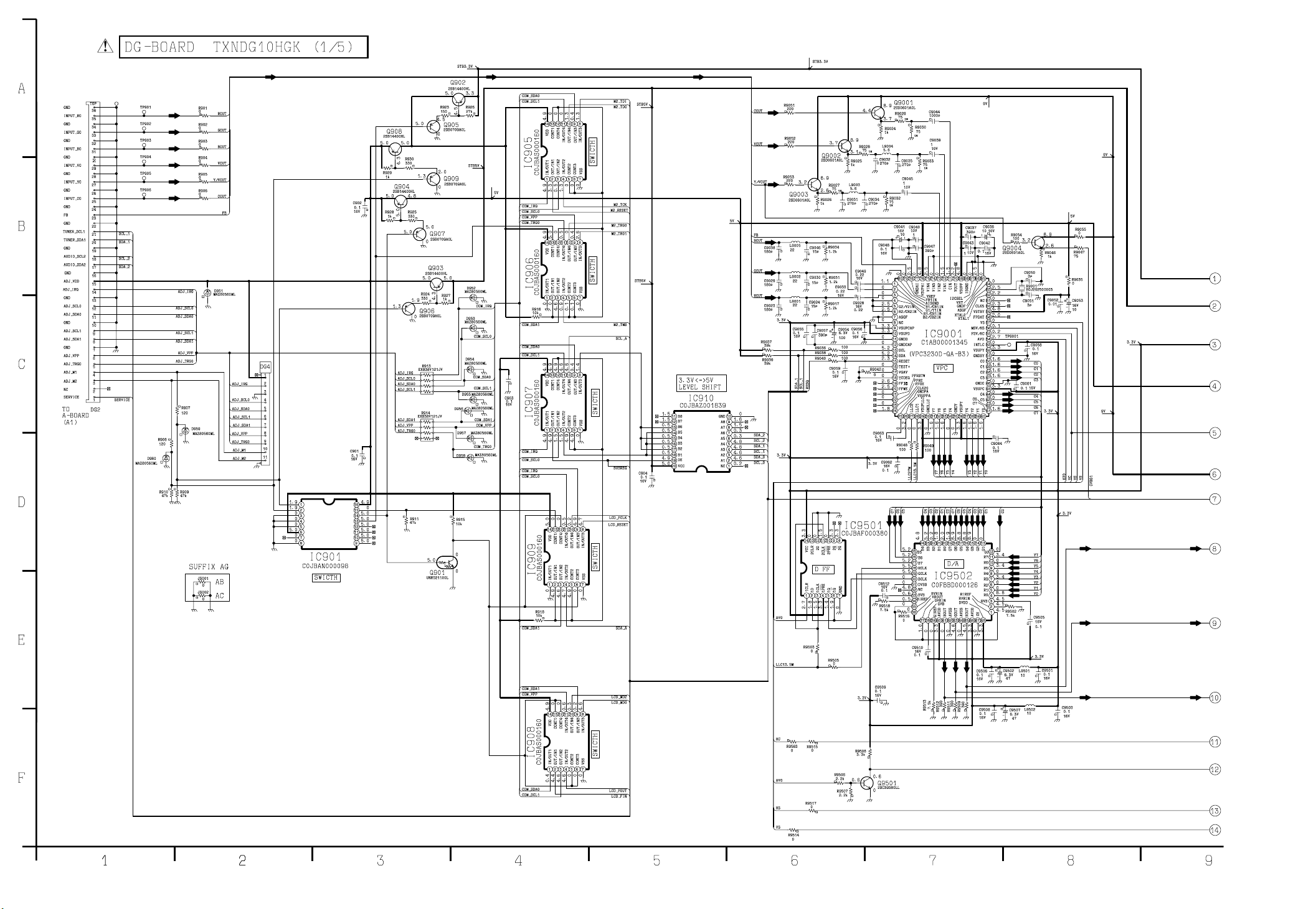
TX-15LT2M/Q/T/X/Z DG-Board (1 of 5) Schematic Diagram TX-15LT2M/Q/T/X/Z DG-Board (1 of 5) Schematic Diagram
Page 39
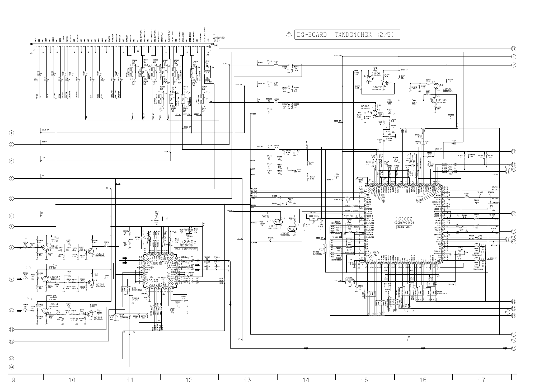
TX-15LT2M/Q/T/X/Z DG-Board (2 of 5) Schematic Diagram TX-15LT2M/Q/T/X/Z DG-Board (2 of 5) Schematic Diagram
Page 40
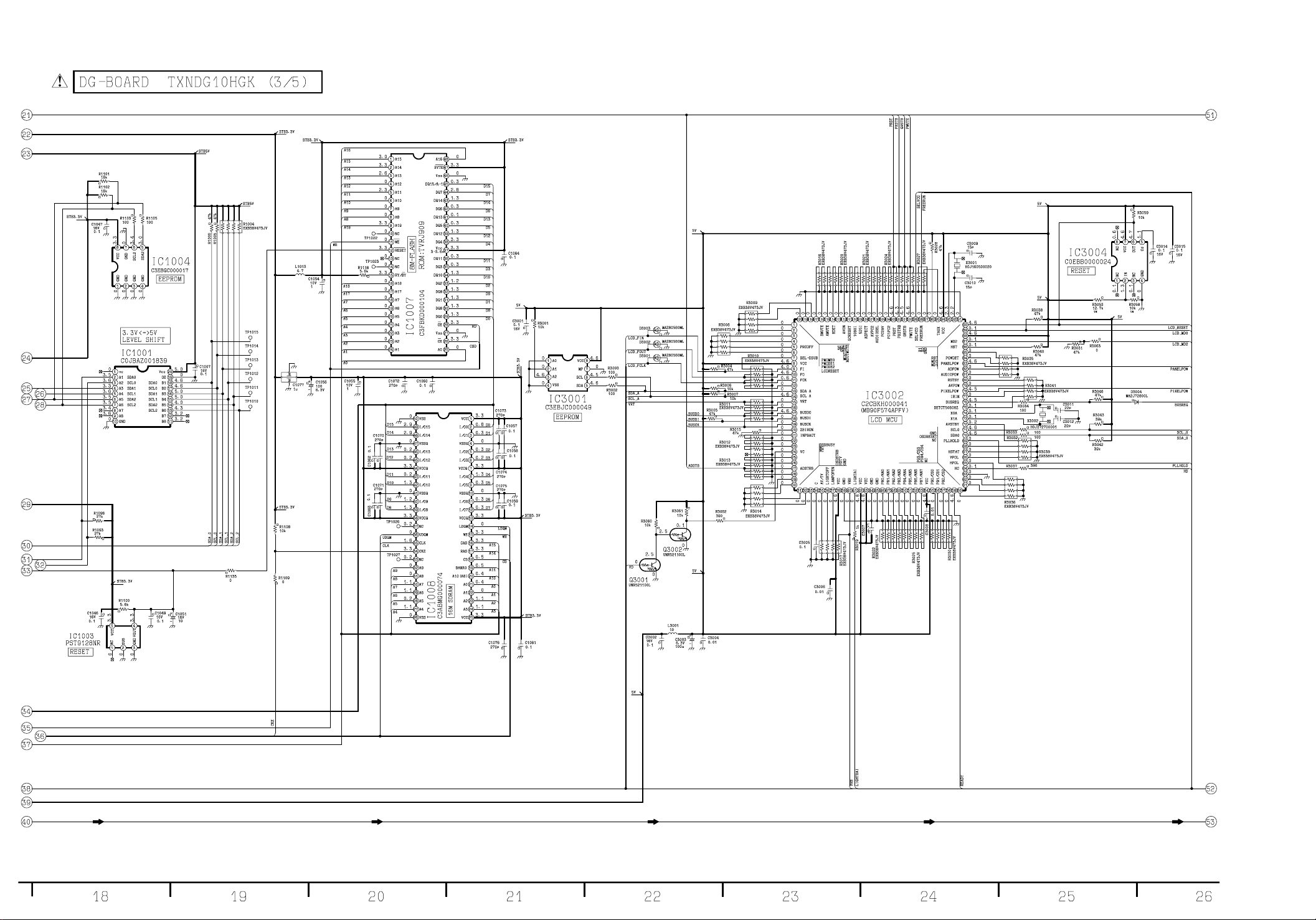
TX-15LT2M/Q/T/X/Z
DG-Board (3 of 5) Schematic Diagram
TX-15LT2M/Q/T/X/Z
DG-Board (3 of 5) Schematic Diagram
Page 41
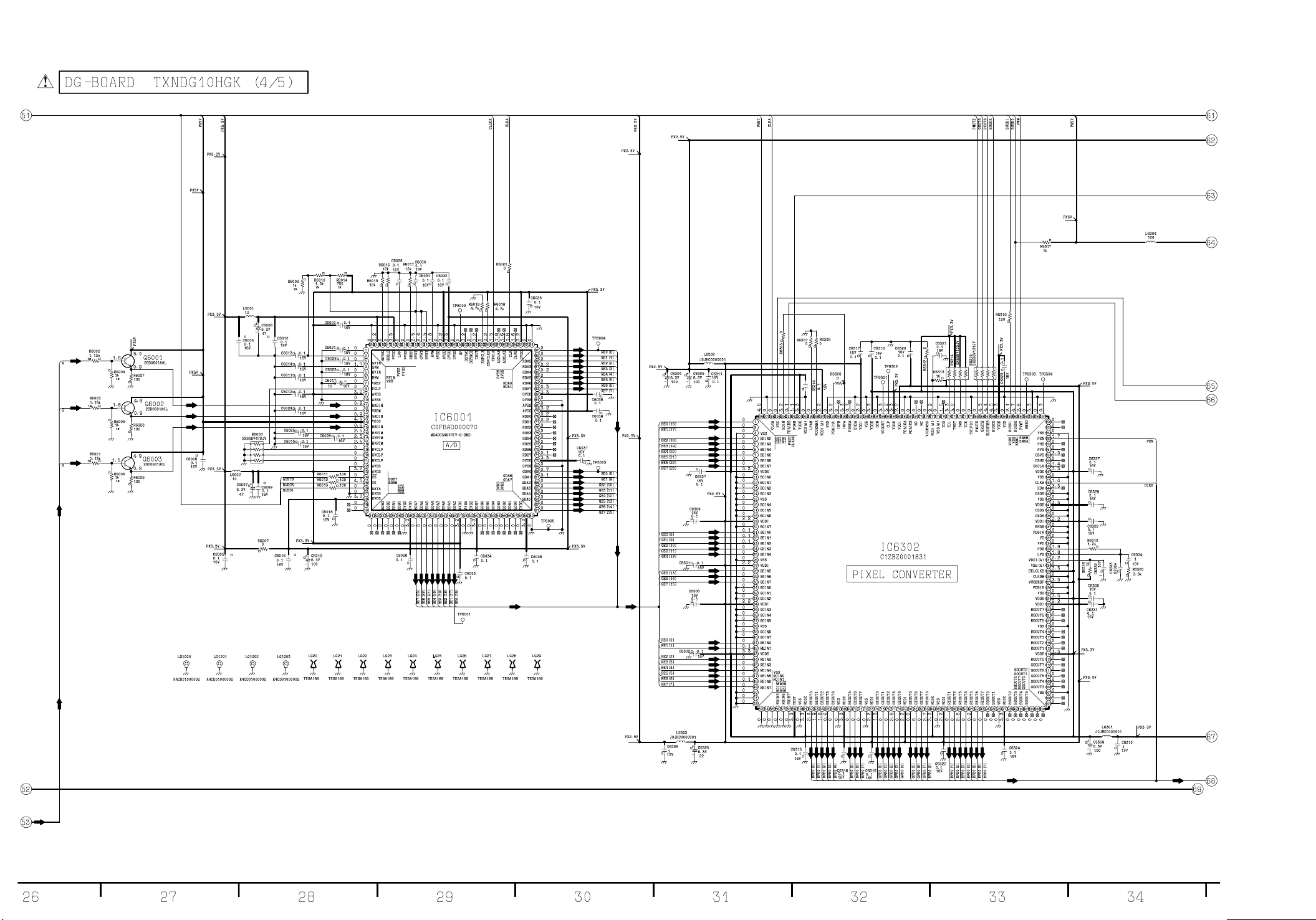
TX-15LT2M/Q/T/X/Z
DG-Board (4 of 5) Schematic Diagram
TX-15LT2M/Q/T/X/Z
DG-Board (4 of 5) Schematic Diagram
Page 42
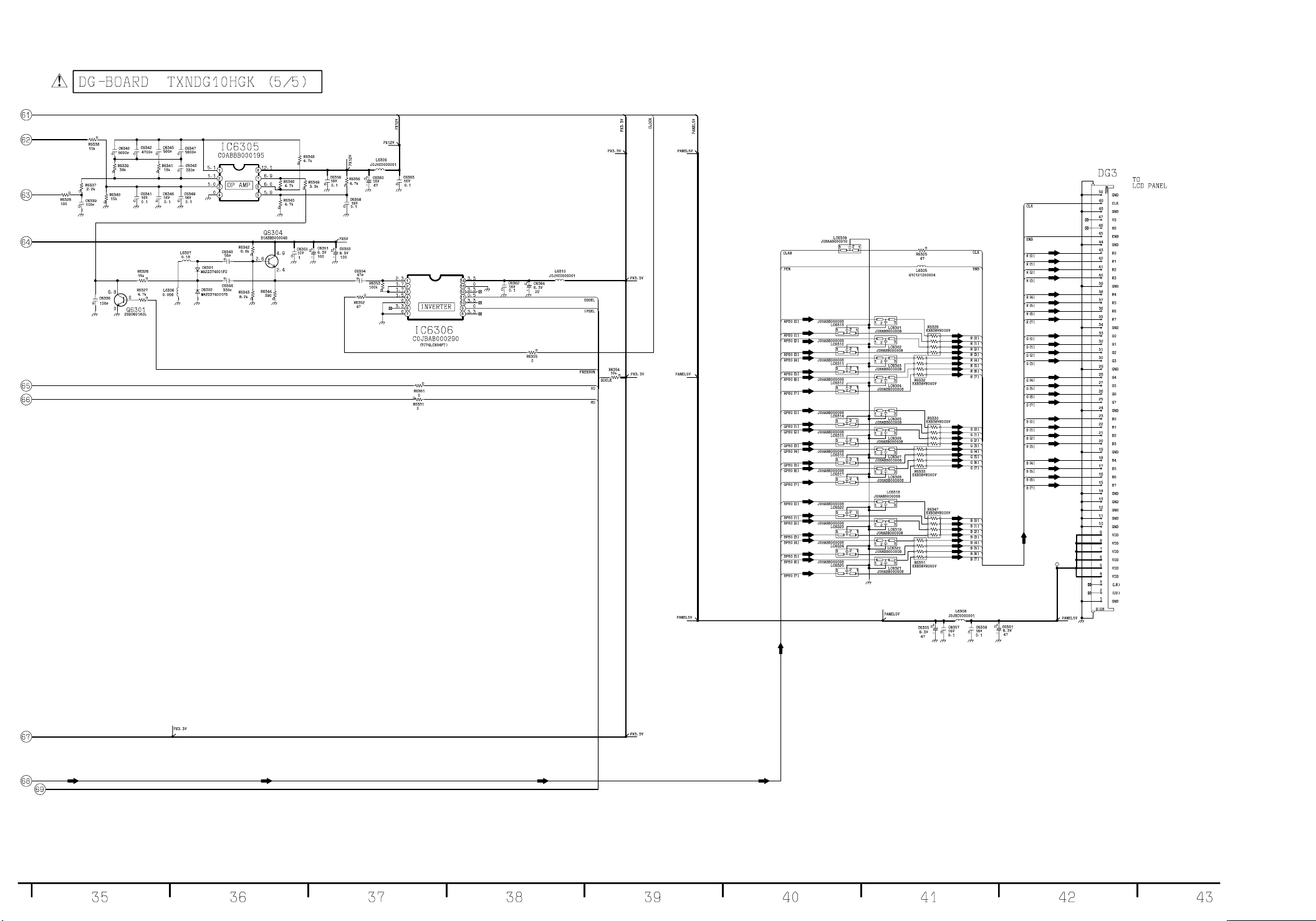
TX-15LT2M/Q/T/X/Z
DG-Board (5 of 5) Schematic Diagram
TX-15LT2M/Q/T/X/Z
DG-Board (5 of 5) Schematic Diagram
Page 43
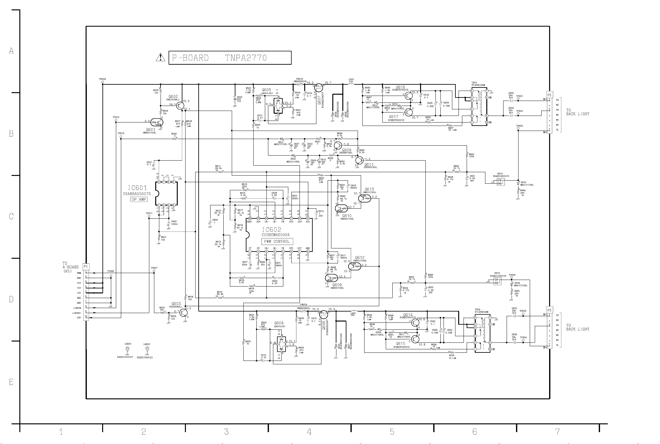
TX-15LT2M/Q/T/X/Z
P-Board Schematic Diagram
TX-15LT2M/Q/T/X/Z
P-Board Schematic Diagram
Page 44
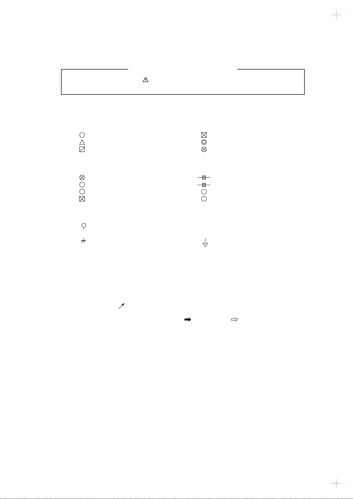
11 Block and Schematic Diagrams
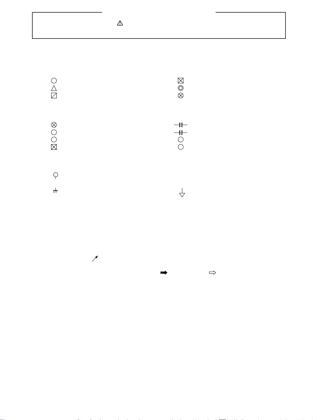
11.1. Schematic Diagram Notes
Important Safety Notice
Components identified by mark have special characteristics important for safety.
When replacing any of these components, use only manufacture's specified parts.
Notes:
1. Resistor
All resistors are cabon 1/4W resistor, unless marked as follows:
Unit of resistance is OHM [W] (K=1,000, M=1,000,000).
: Nonflammable : Metal Oxide
: Solid : Metal Film
: Wire Wound : Fuse:
2. Capacitor
All capacitors are ceramic 50V capacitor, unless marked as follows:
Unit of capacitance is mF, unless otherwise noted.
: Temperature Compensation : Electrolytic
: Polyester : Bipolar
M
m T
: Metalized Polyester : Dipped Tantalum
: Polypropylene : Z-Type
3. Coil
Unit of inductance is mF, unless otherwise noted.
4. Test Point
: Test Point position
5. Earth Symbol
: Chassis Earth (Cold) : Line Earth (Hot)
6. Voltage Measurement
Voltage is measured by a DC voltmeter.
Conditions of the measurement are the following:
Power Source ................................................... AC 100-240V, 50/60Hz
Receiving Signal ............................................... Colour Bar signal (RF)
All customer's controls ...................................... Maximum positions
7. Number in red circle indicates waveform nember.
(See waveform pattern table.)
8. When arrow mark ( ) is found, connection is easily found from the direction of arrow
NP
+
-
Z
9. Indicates the major signal flow. : Video Audio
10. This schematic diagram is the latest at the time of printing and subject to change without
notice.
TX-15LT2M/Q/T/X/Z
Schematic Diagram Notes
29
Page 45

Remarks:
1. The Power Circuit contains a circuit area which uses a separate power supply to isolate the
earth connection.
The circuit is defined by HOT and COLD indications in the schematic diagram. Take the
follwing precautions.
All circuits, except the Power Circuit, are cold.
Precautions
a. Do not touch the hot part or the hot and cold parts at the same time or you may
be shocked.
b. Do not short- circuit the hot and cold circuits or a fuse may blow and parts may
break.
c. Do not connect an instrument, such as an oscilloscope, to the hot and cold
circuits simultaneously or a fuse may blow.
Connect the earth of instruments to the earth connection of the circuit being
measured.
d. Make sure to disconnect the power plug before removing the chassis.
2. Following diodes are interchangeable.
MA150- MA162 (Replacement part)
29
TX-15LT2M/Q/T/X/Z
Schematic Diagram Notes
Page 46
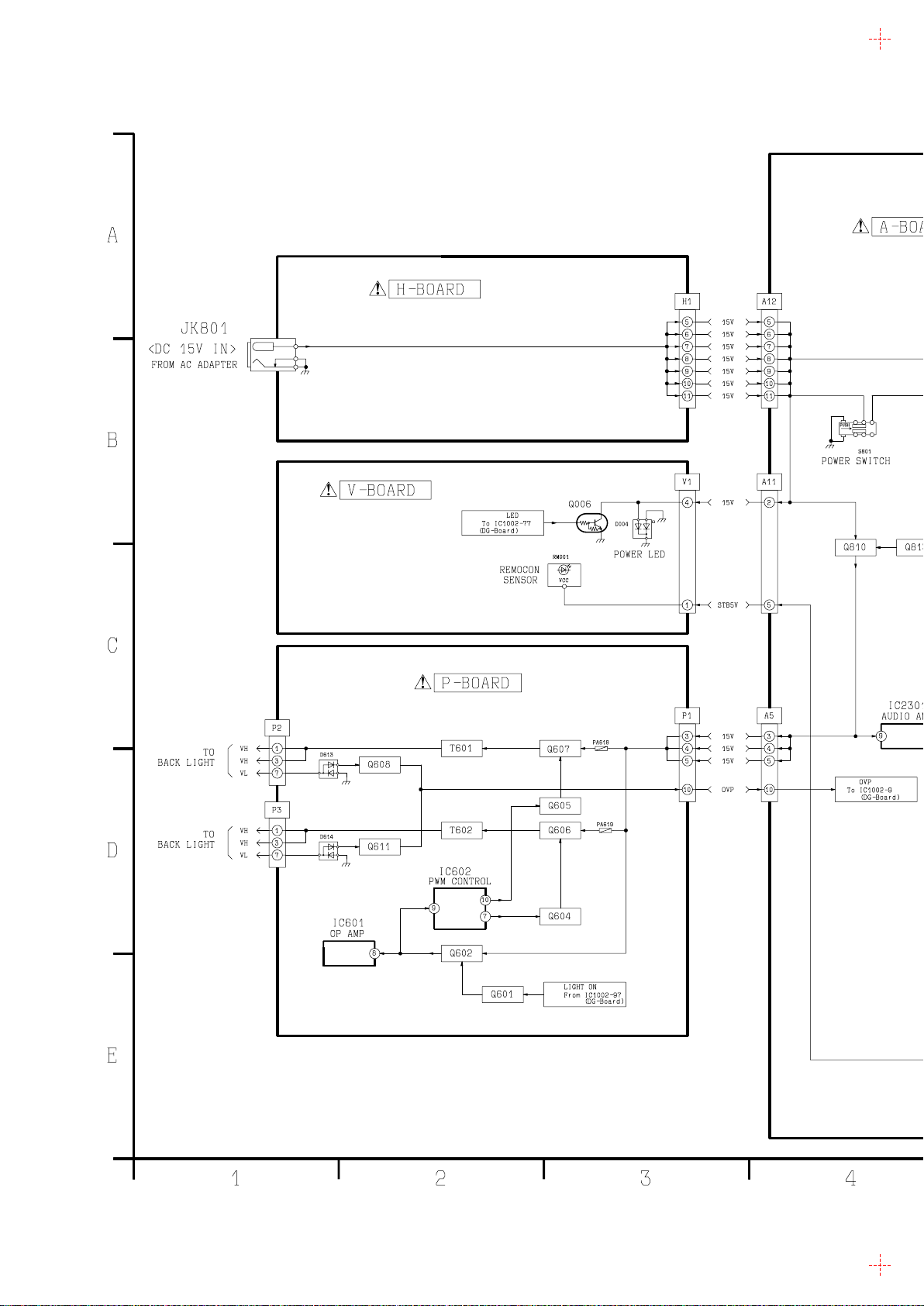
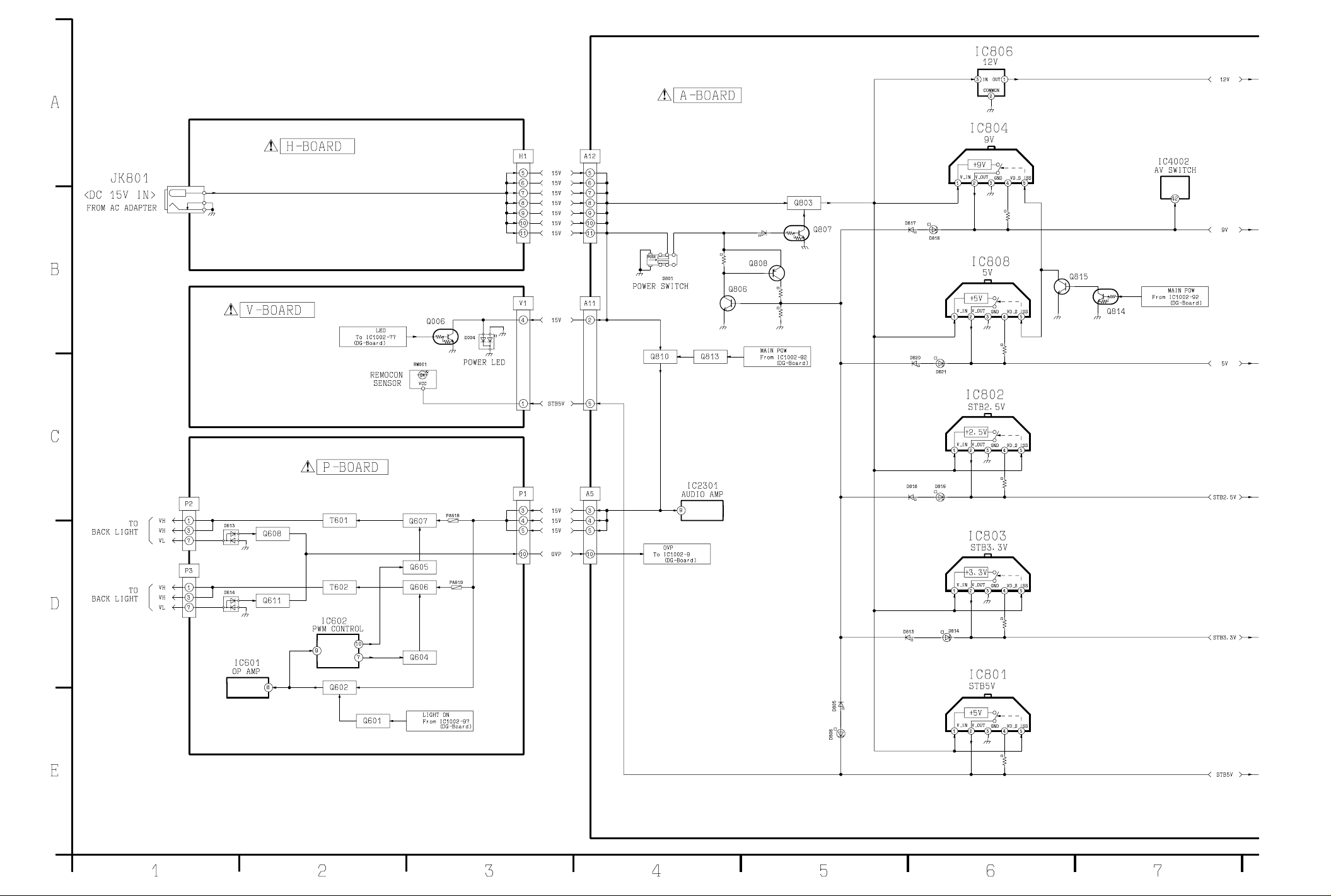
11.2. Power Block Diagram
TX-15LT2M/Q/T/X/Z Power Block Diagram TX-15LT2M/Q/T/X/Z Power Block Diagram
30
Page 47
30
Page 48
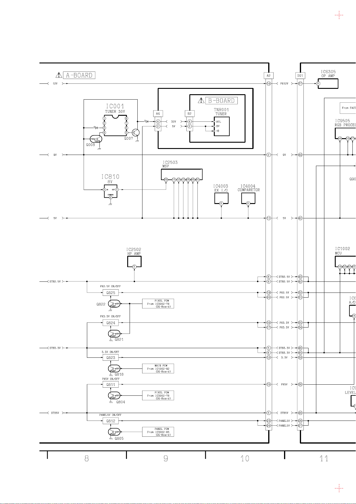
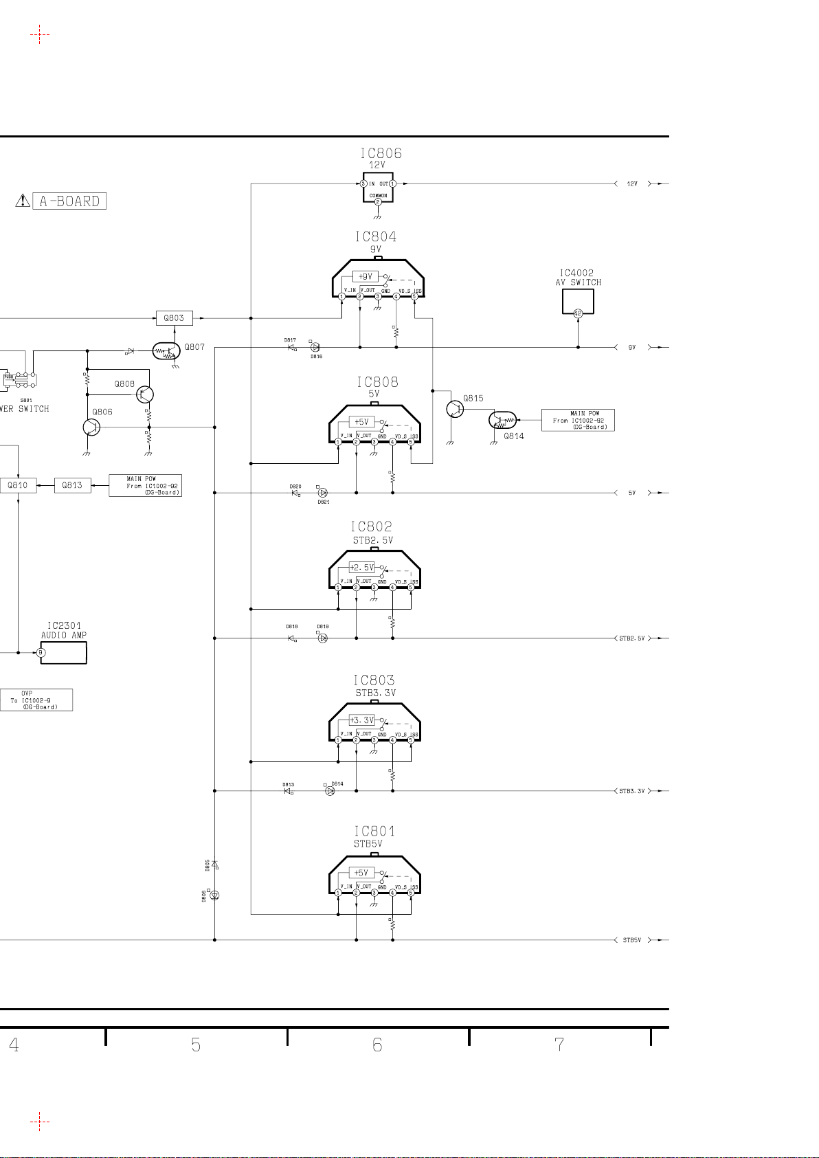
TX-15LT2M/Q/T/X/Z Power Block Diagram TX-15LT2M/Q/T/X/Z Power Block Diagram
31
Page 49
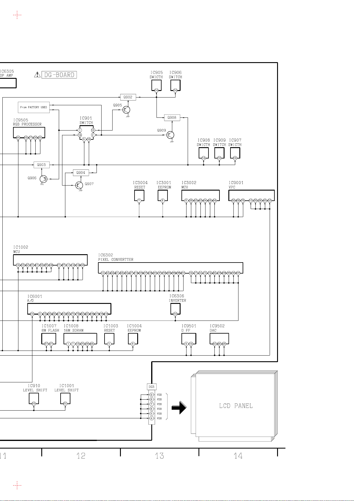
31
Page 50
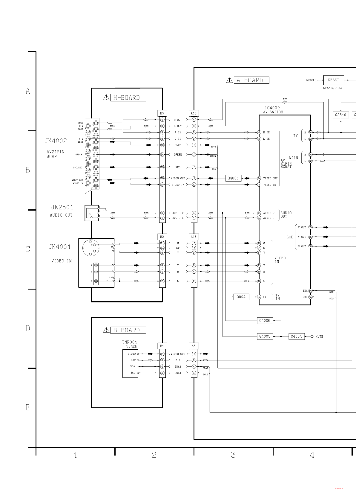
11.3. Signal Block Diagram
TX-15LT2M/Q/T/X/Z Signal Block Diagram TX-15LT2M/Q/T/X/Z Signal Block Diagram
32
Page 51
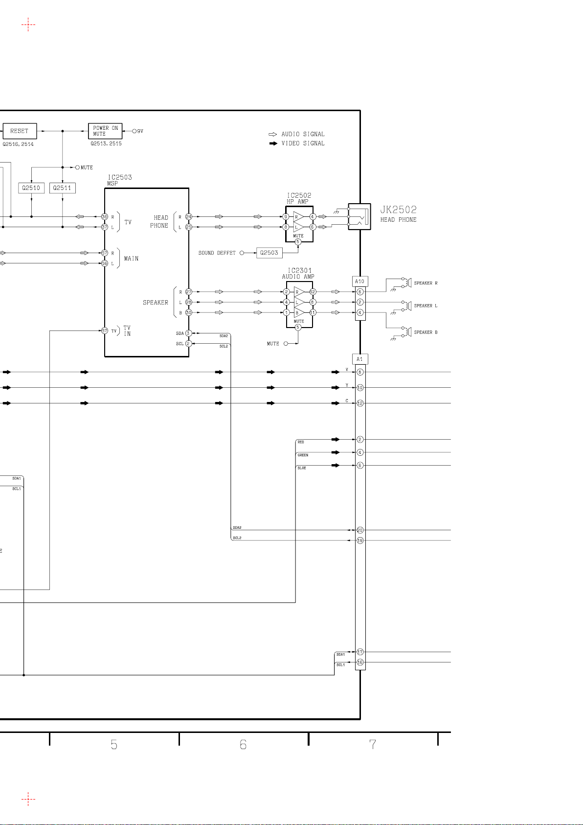
32
Page 52
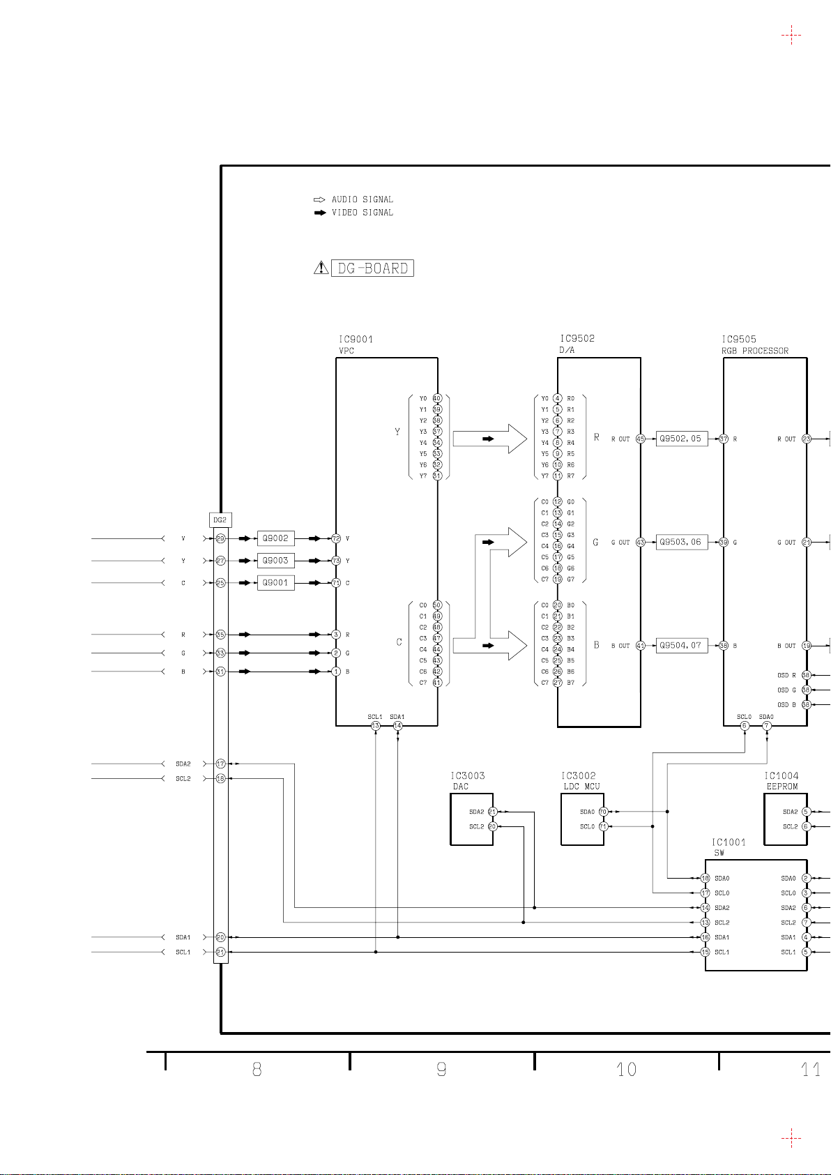
TX-15LT2M/Q/T/X/Z Signal Block Diagram TX-15LT2M/Q/T/X/Z Signal Block Diagram
33
Page 53
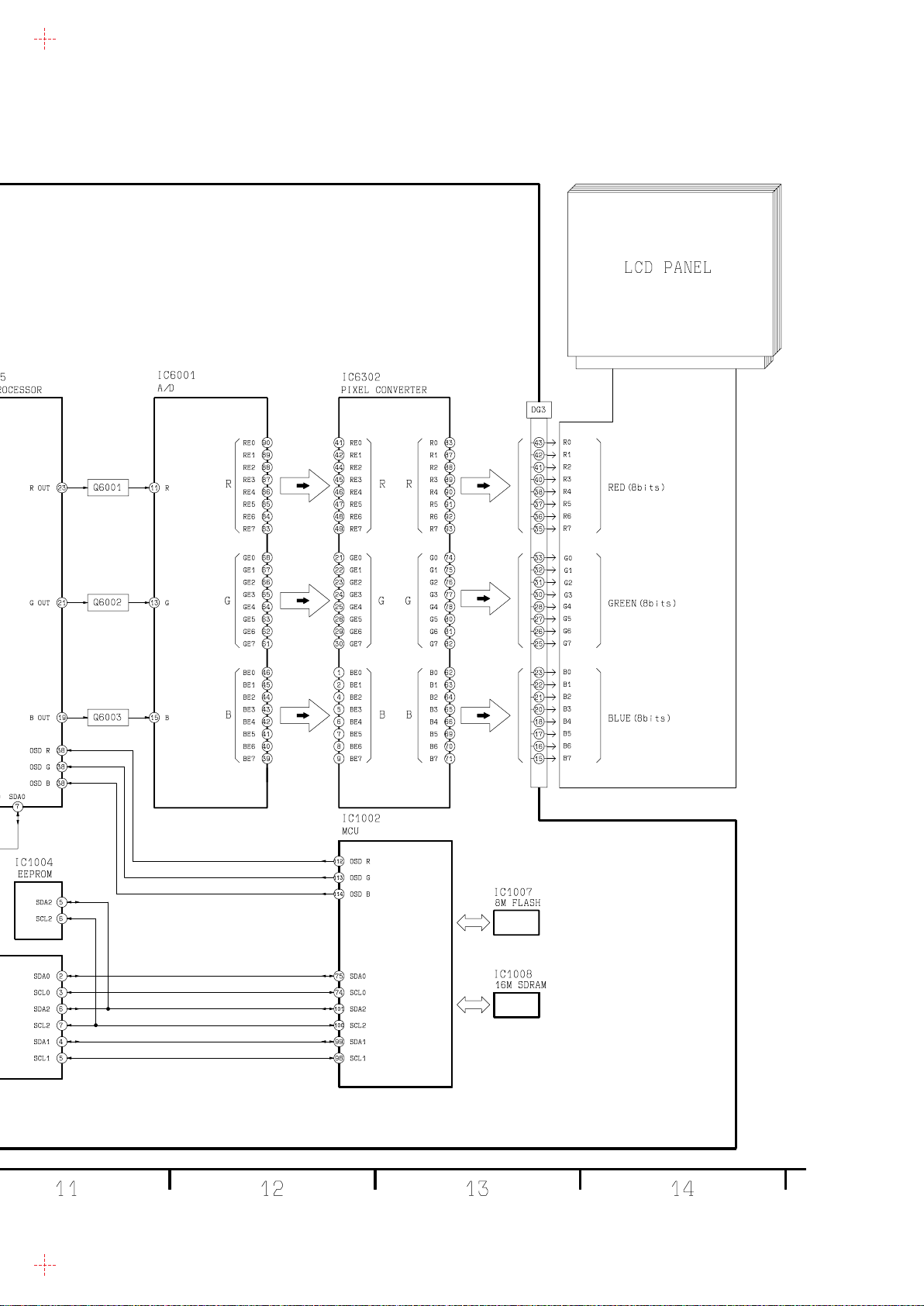
33
Page 54
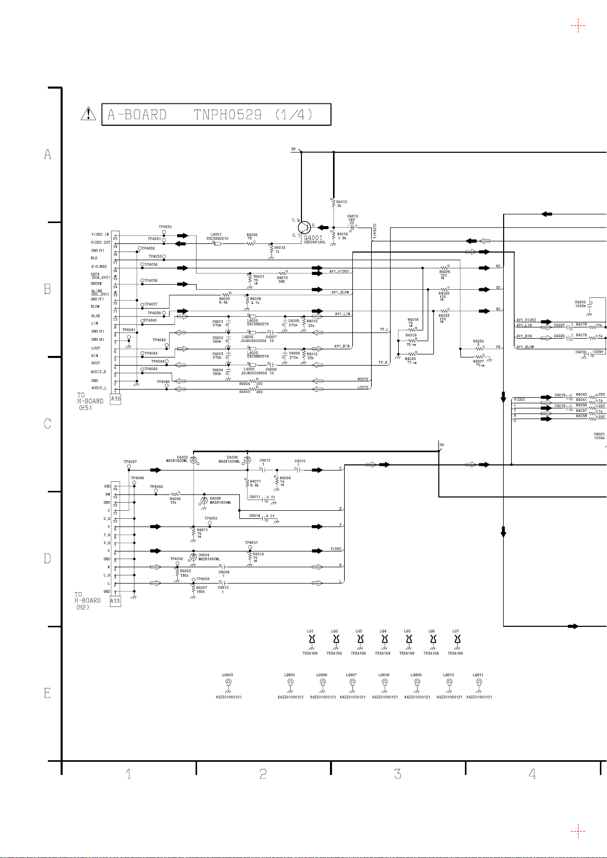
11.4. A-Board (1 of 4) Schematic Diagram
TX-15LT2M/Q/T/X/Z
A-Board (1 of 4) Schematic Diagram
34
Page 55
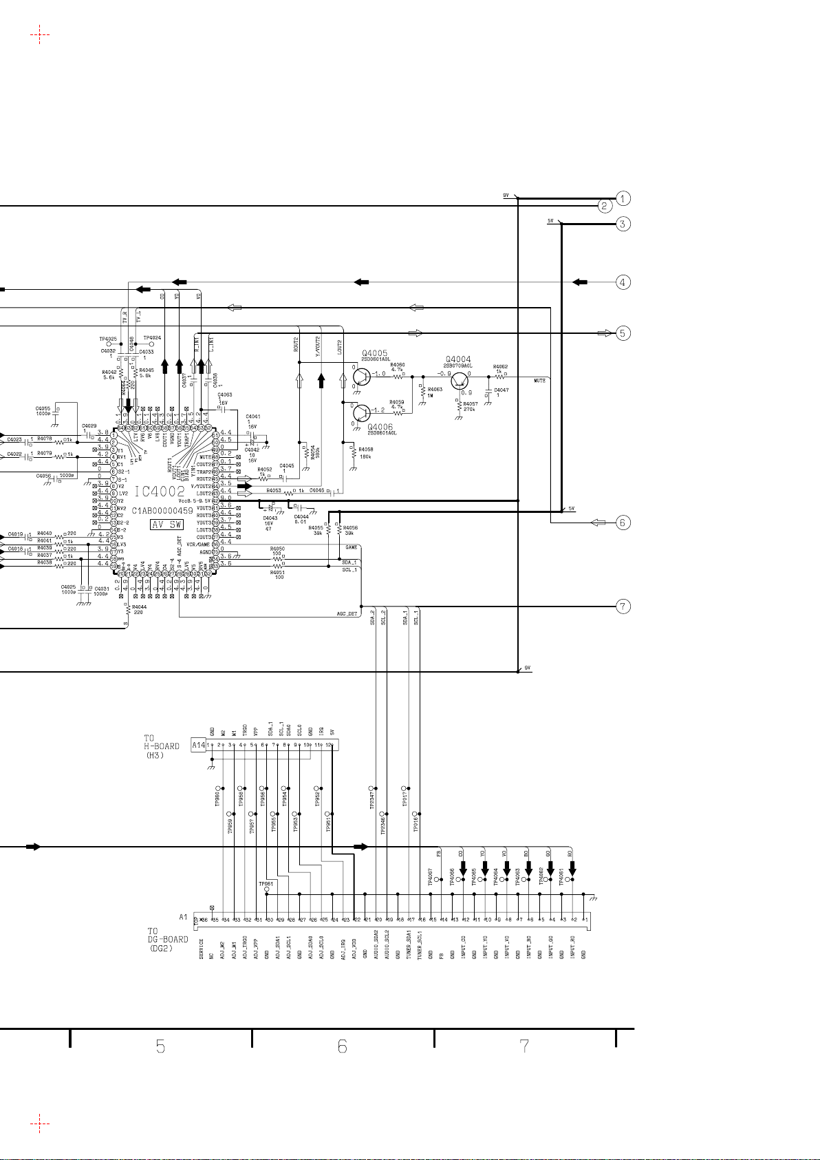
34
TX-15LT2M/Q/T/X/Z
A-Board (1 of 4) Schematic Diagram
Page 56
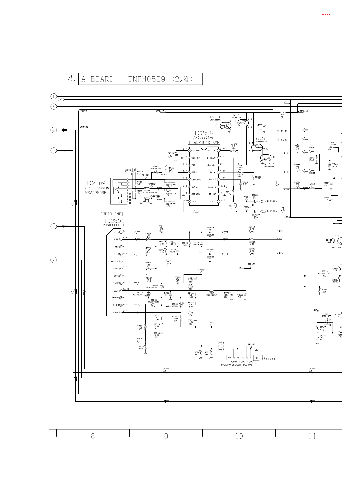
11.5. A-Board (2 of 4) Schematic Diagram
TX-15LT2M/Q/T/X/Z
A-Board (2 of 4) Schematic Diagram
35
Page 57
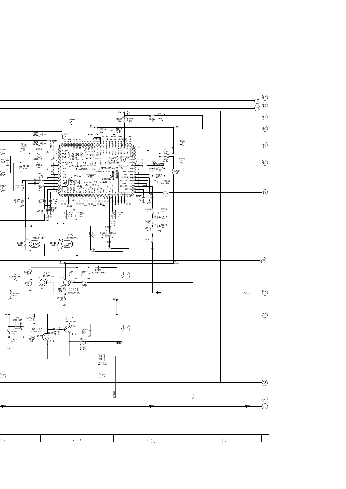
35
TX-15LT2M/Q/T/X/Z
A-Board (2 of 4) Schematic Diagram
Page 58
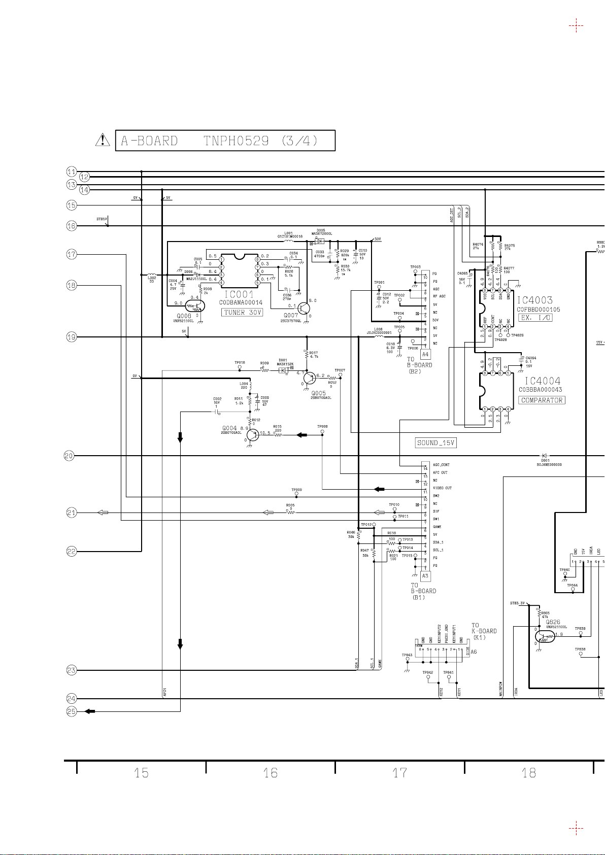
11.6. A-Board (3 of 4) Schematic Diagram
TX-15LT2M/Q/T/X/Z
A-Board (3 of 4) Schematic Diagram
36
Page 59
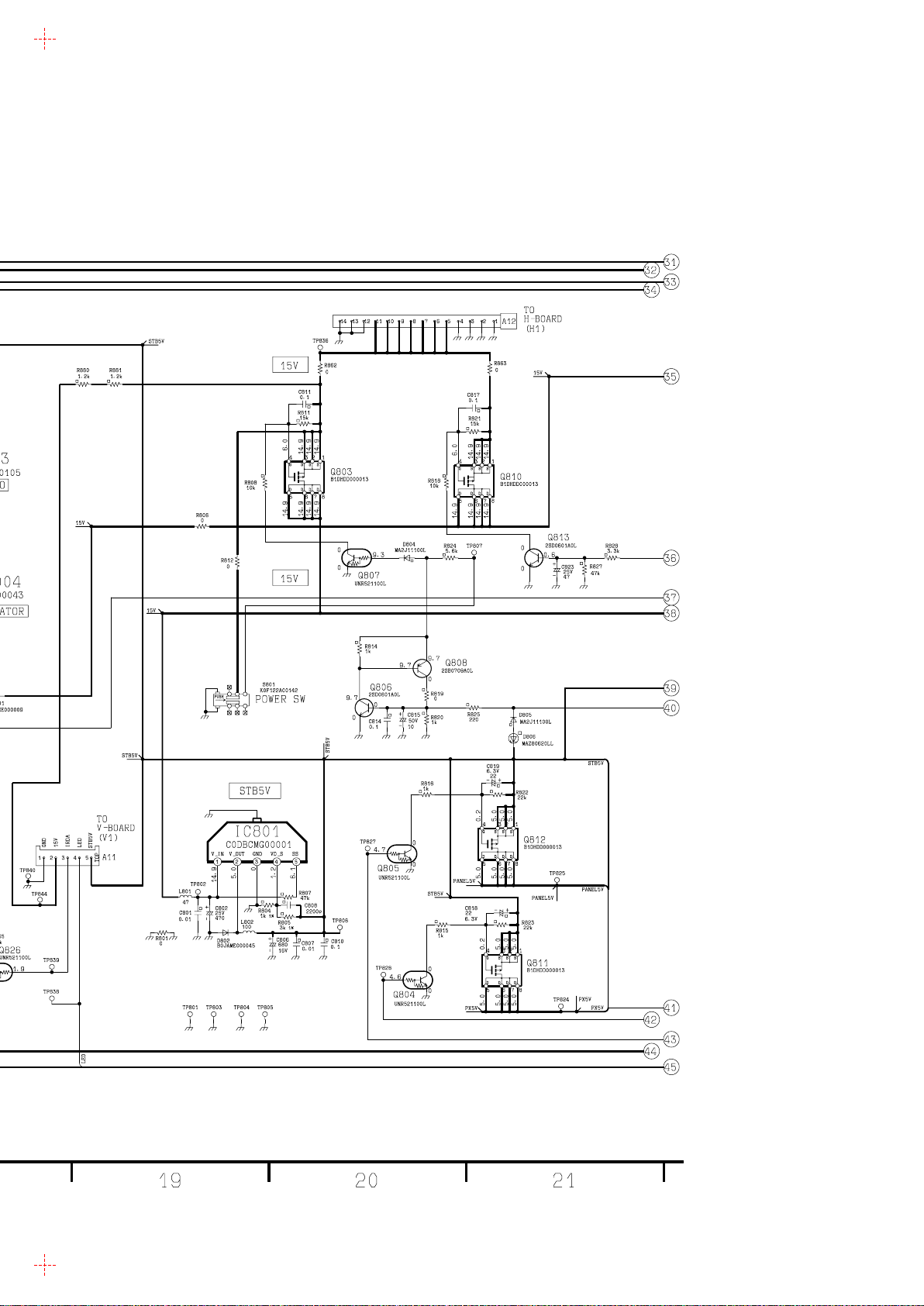
36
TX-15LT2M/Q/T/X/Z
A-Board (3 of 4) Schematic Diagram
Page 60
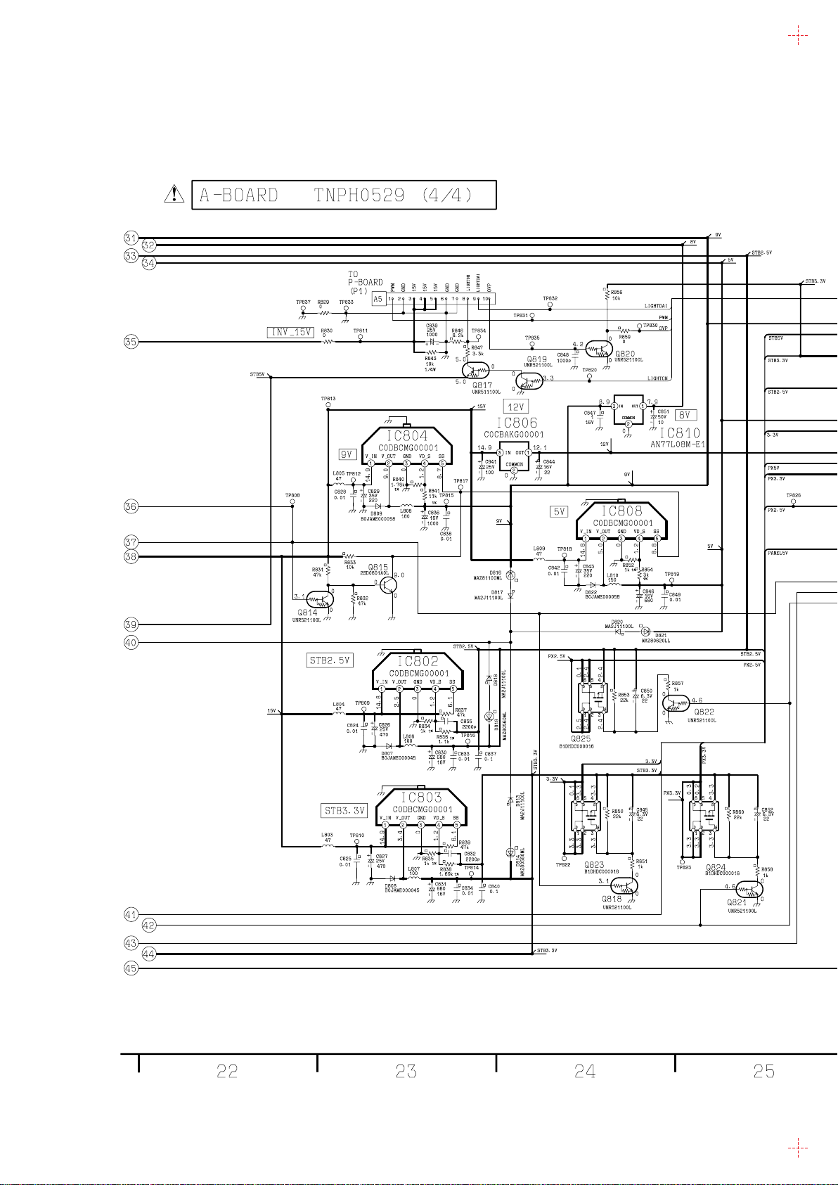
11.7. A-Board (4 of 4) Schematic Diagram
TX-15LT2M/Q/T/X/Z
A-Board (4 of 4) Schematic Diagram
37
Page 61
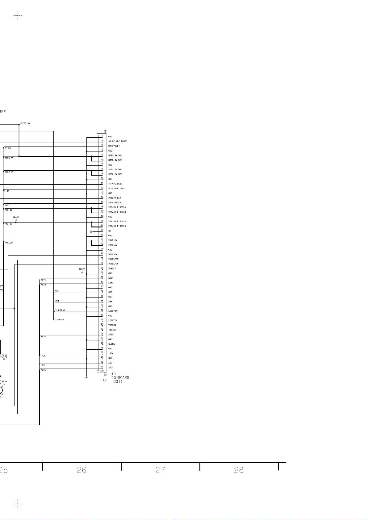
37
TX-15LT2M/Q/T/X/Z
A-Board (4 of 4) Schematic Diagram
Page 62
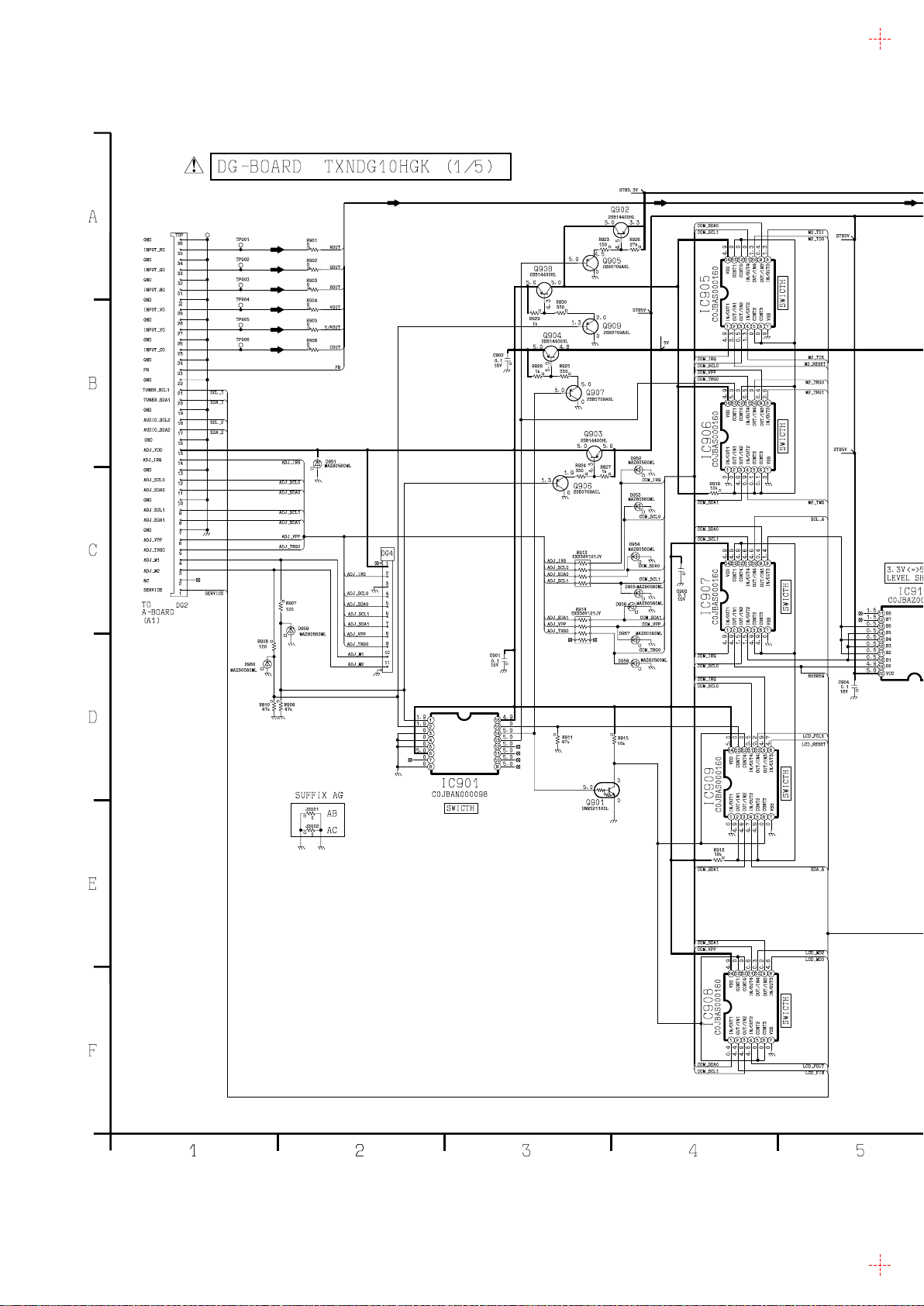
11.8. DG-Board (1 of 5) Schematic Diagram
TX-15LT2M/Q/T/X/Z DG-Board (1 of 5) Schematic Diagram TX-15LT2M/Q/T/X/Z DG-Board (1 of 5) Schematic Diagram
38
Page 63
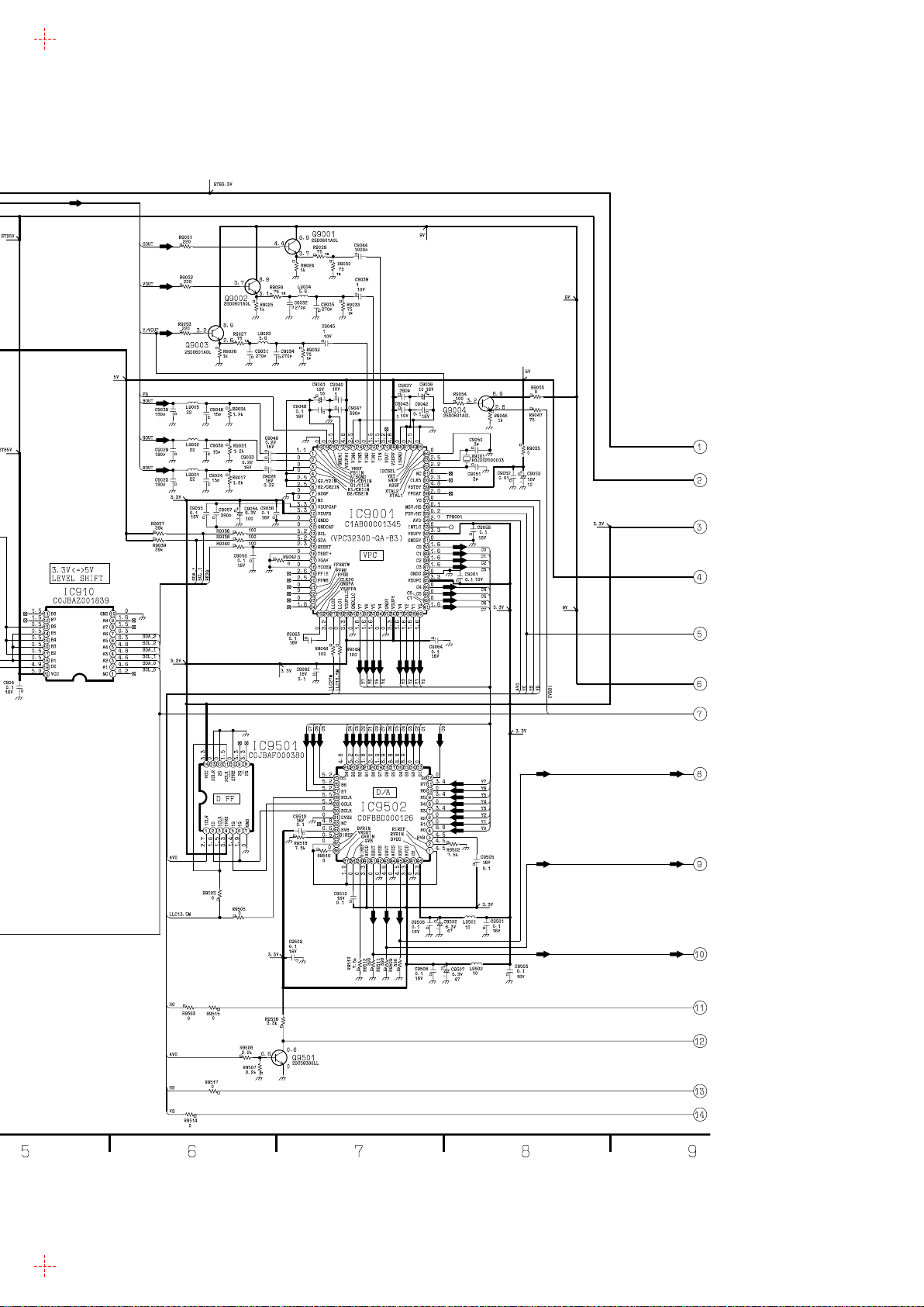
38
Page 64
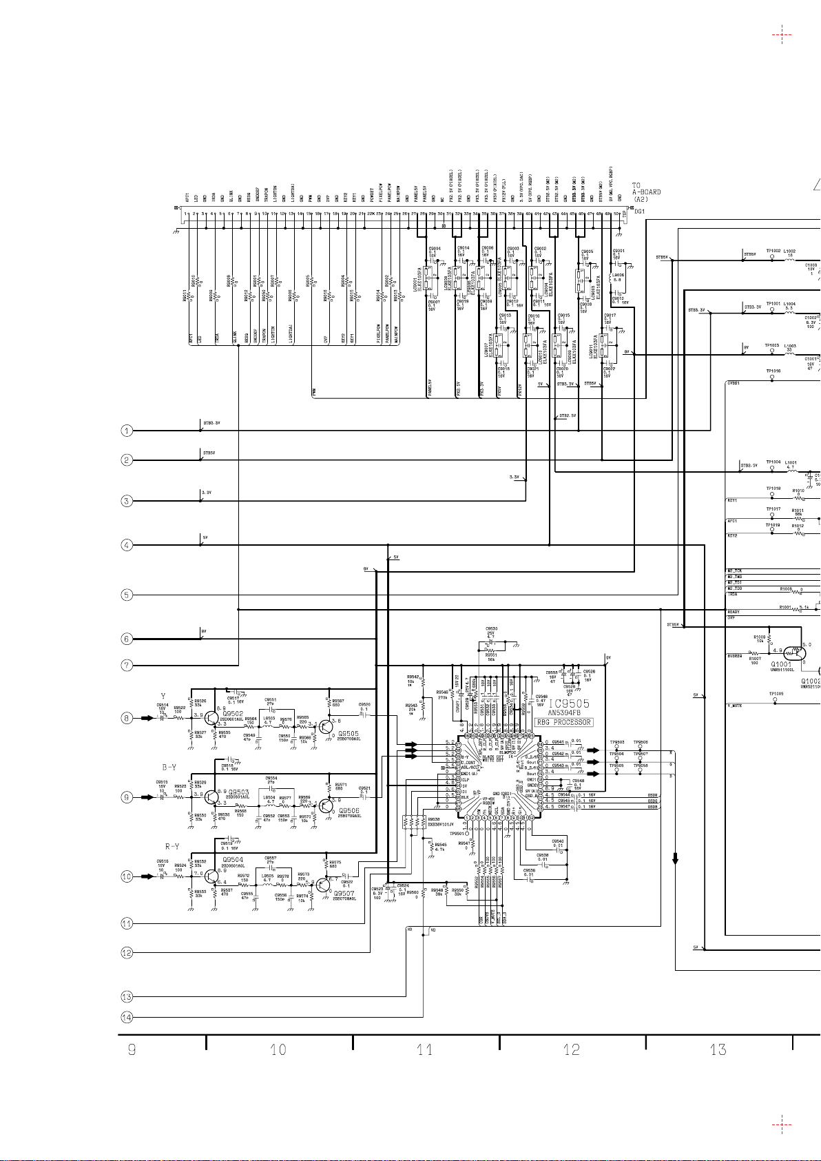
11.9. DG-Board (2 of 5) Schematic Diagram
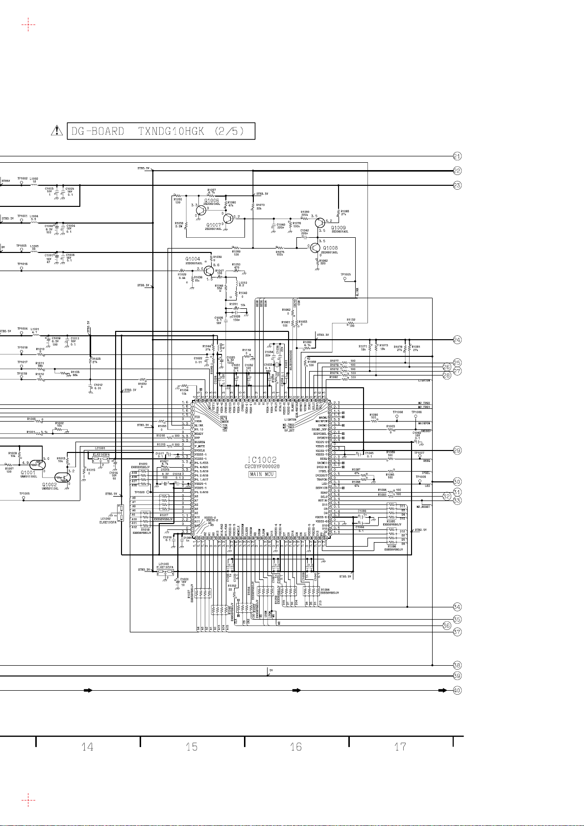
TX-15LT2M/Q/T/X/Z DG-Board (2 of 5) Schematic Diagram TX-15LT2M/Q/T/X/Z DG-Board (2 of 5) Schematic Diagram
39
Page 65
39
Page 66
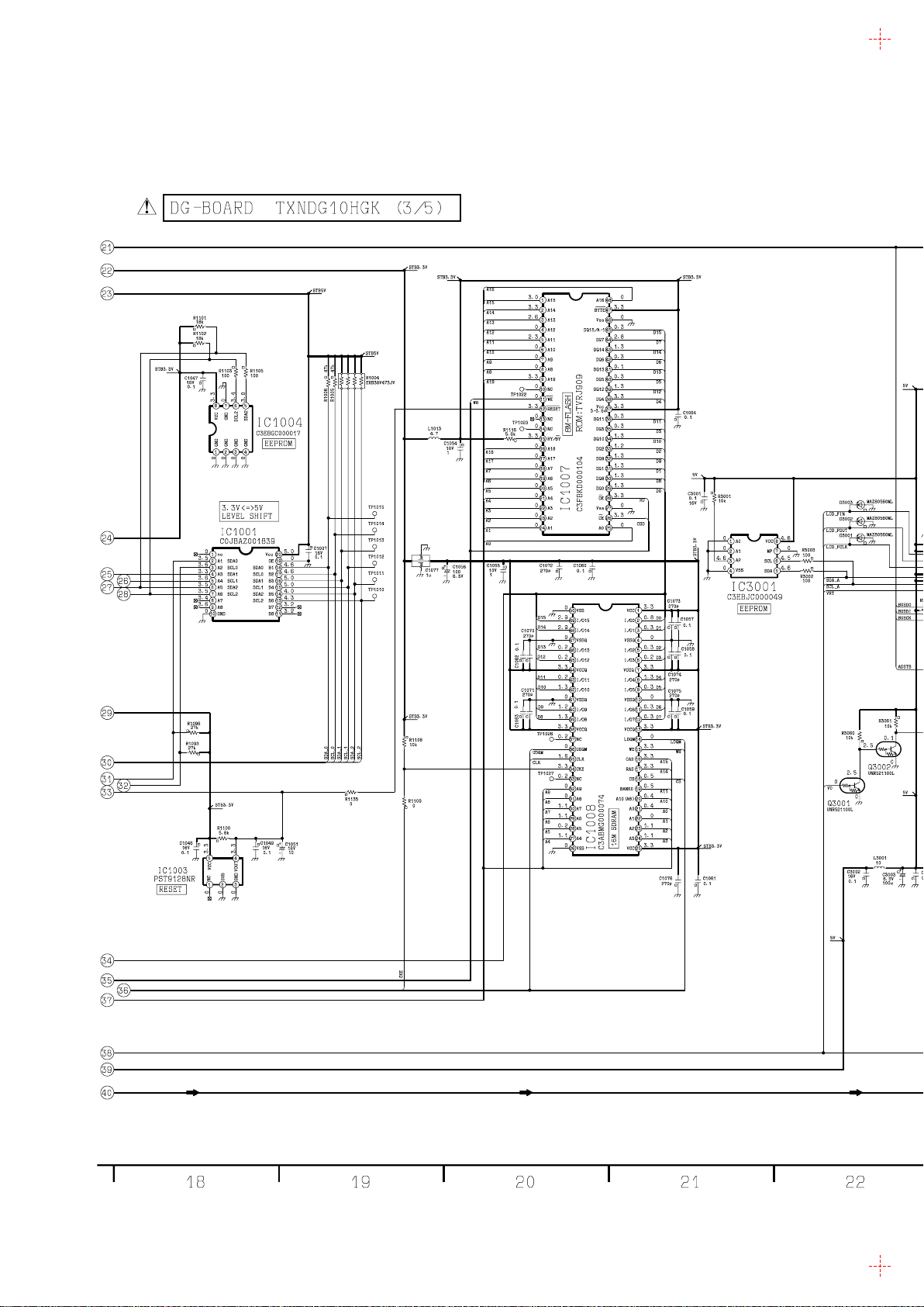
11.10. DG-Board (3 of 5) Schematic Diagram
TX-15LT2M/Q/T/X/Z
DG-Board (3 of 5) Schematic Diagram
40
Page 67
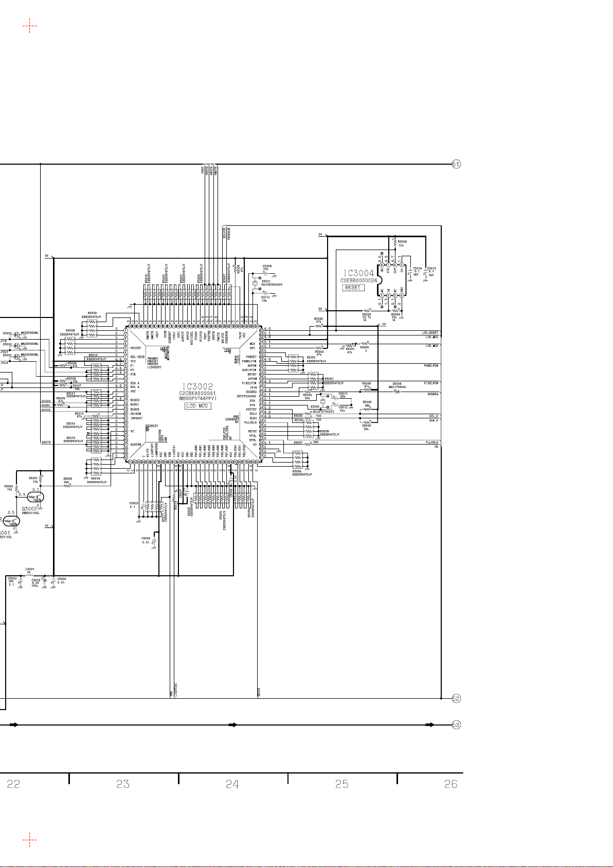
40
TX-15LT2M/Q/T/X/Z
DG-Board (3 of 5) Schematic Diagram
Page 68
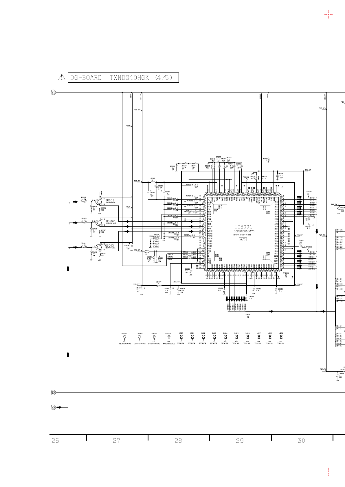
11.11. DG-Board (4 of 5) Schematic Diagram
TX-15LT2M/Q/T/X/Z
DG-Board (4 of 5) Schematic Diagram
41
Page 69
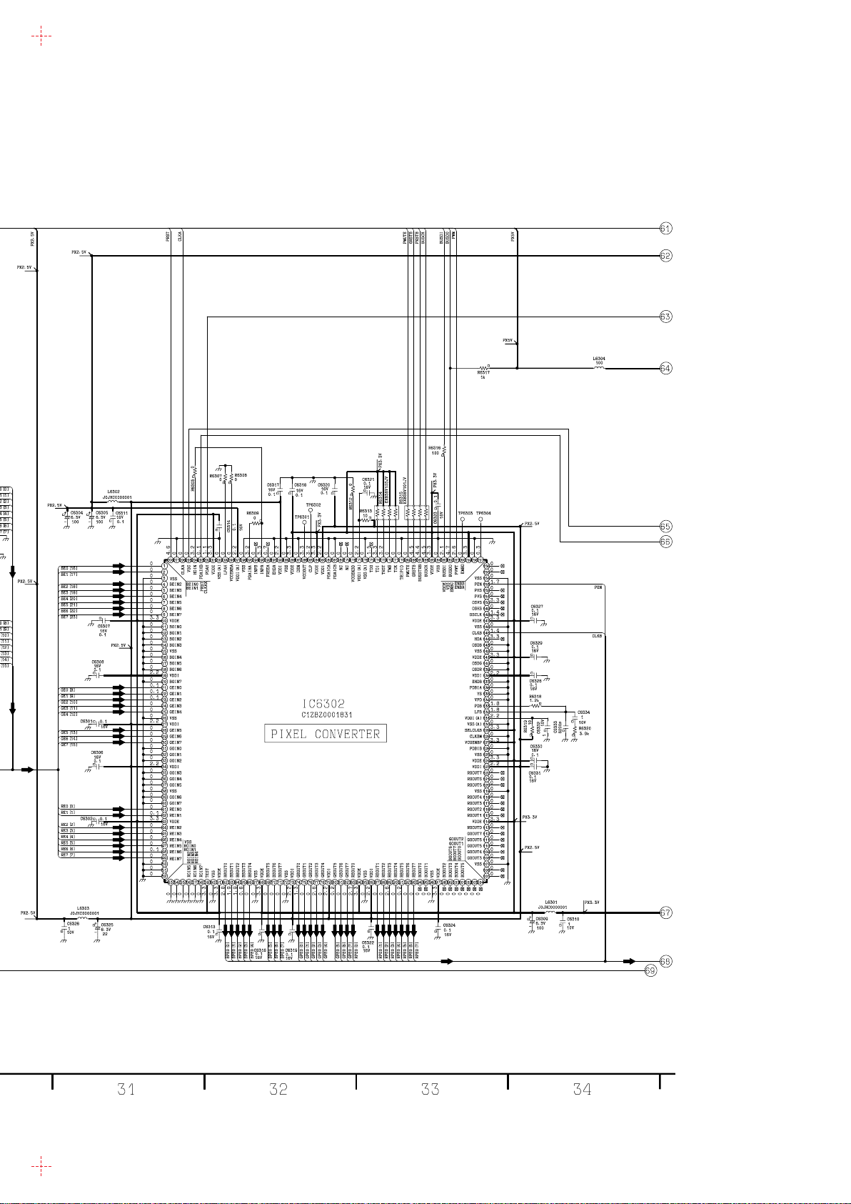
41
TX-15LT2M/Q/T/X/Z
DG-Board (4 of 5) Schematic Diagram
Page 70
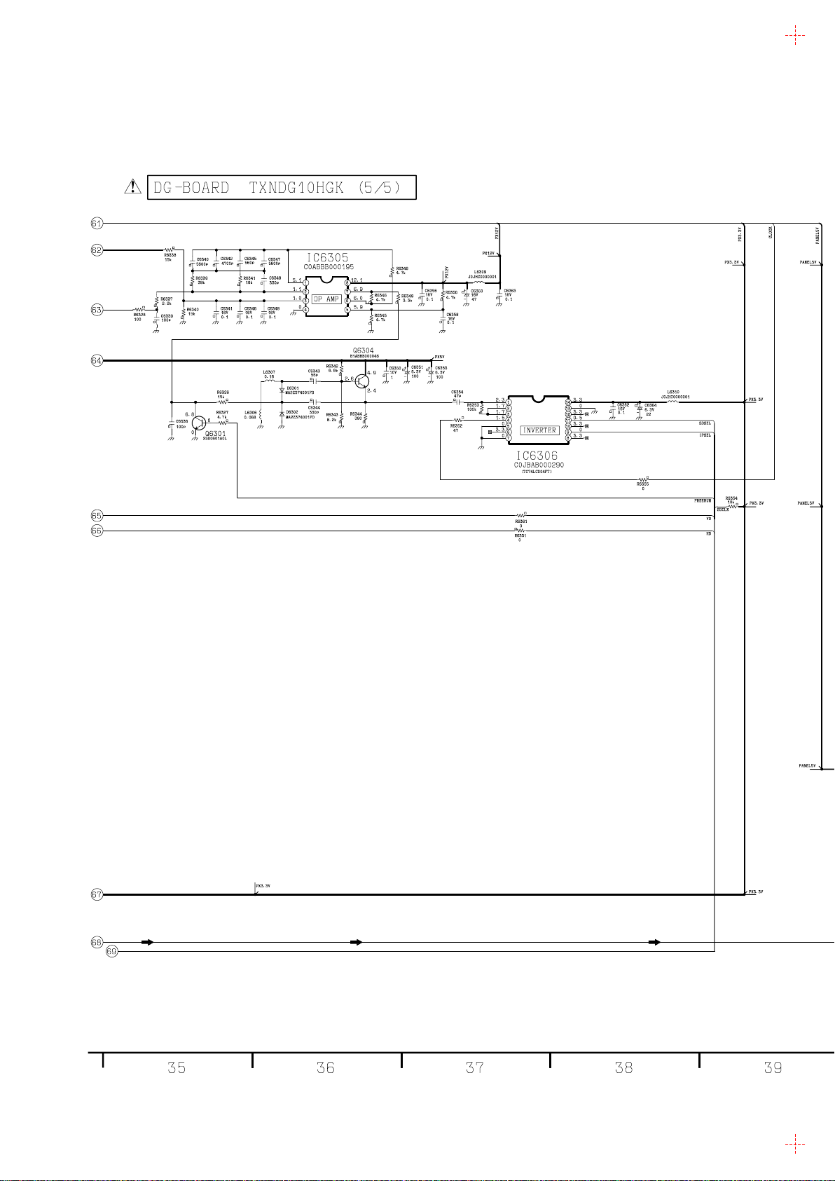
11.12. DG-Board (5 of 5) Schematic Diagram
TX-15LT2M/Q/T/X/Z
DG-Board (5 of 5) Schematic Diagram
42
Page 71
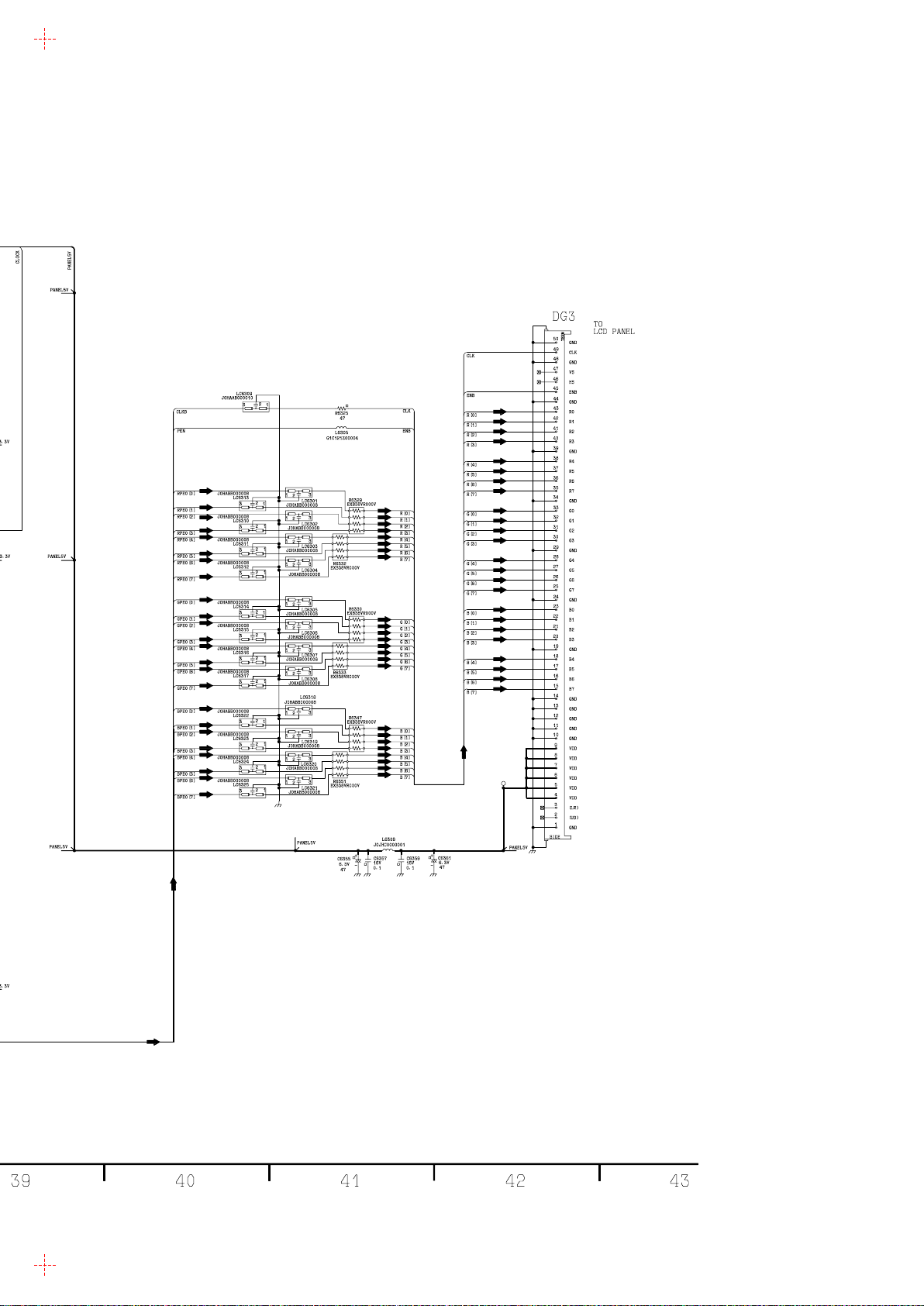
42
TX-15LT2M/Q/T/X/Z
DG-Board (5 of 5) Schematic Diagram
Page 72
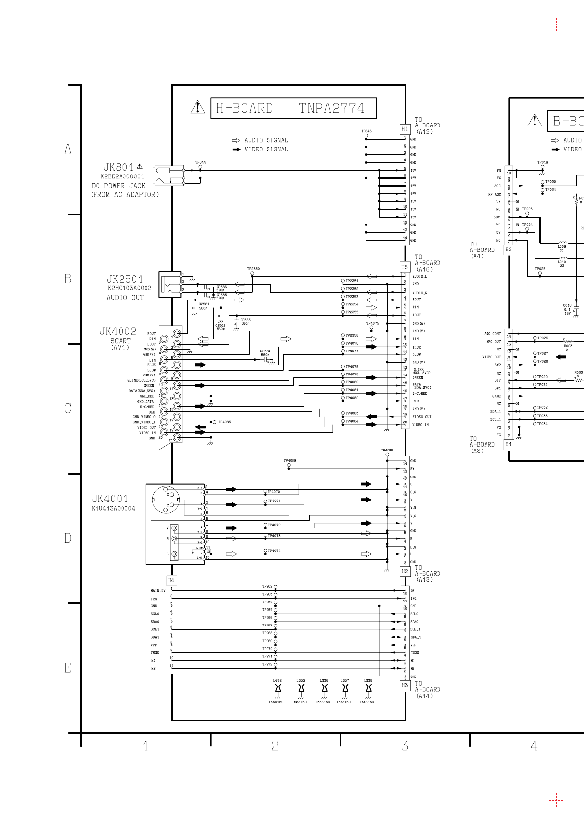
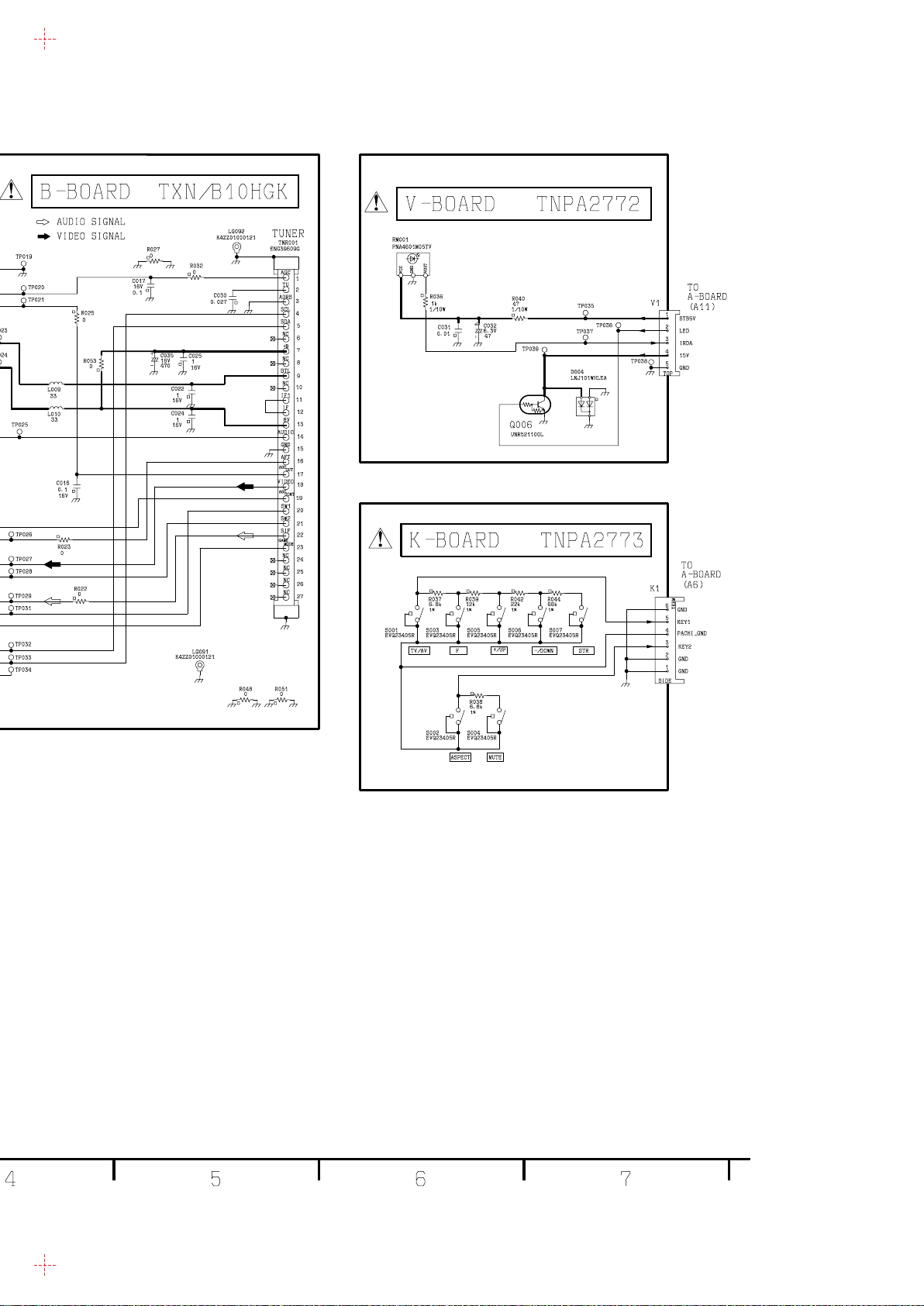
11.13. B, H, K, and V-Board Schematic Diagram
TX-15LT2M/Q/T/X/Z B,H,K,and V-Board Schematic Diagram TX-15LT2M/Q/T/X/Z B,H,K,and V-Board Schematic Diagram
43
Page 73
43
Page 74
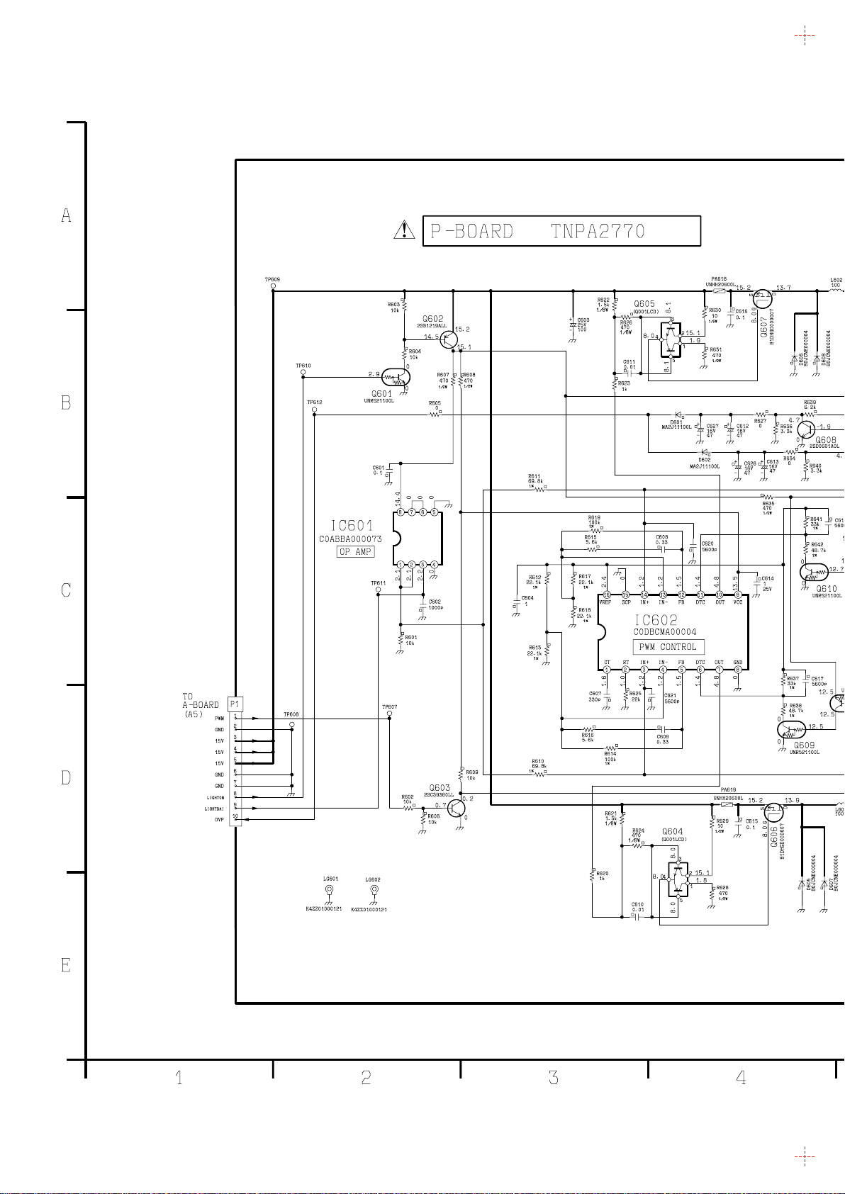
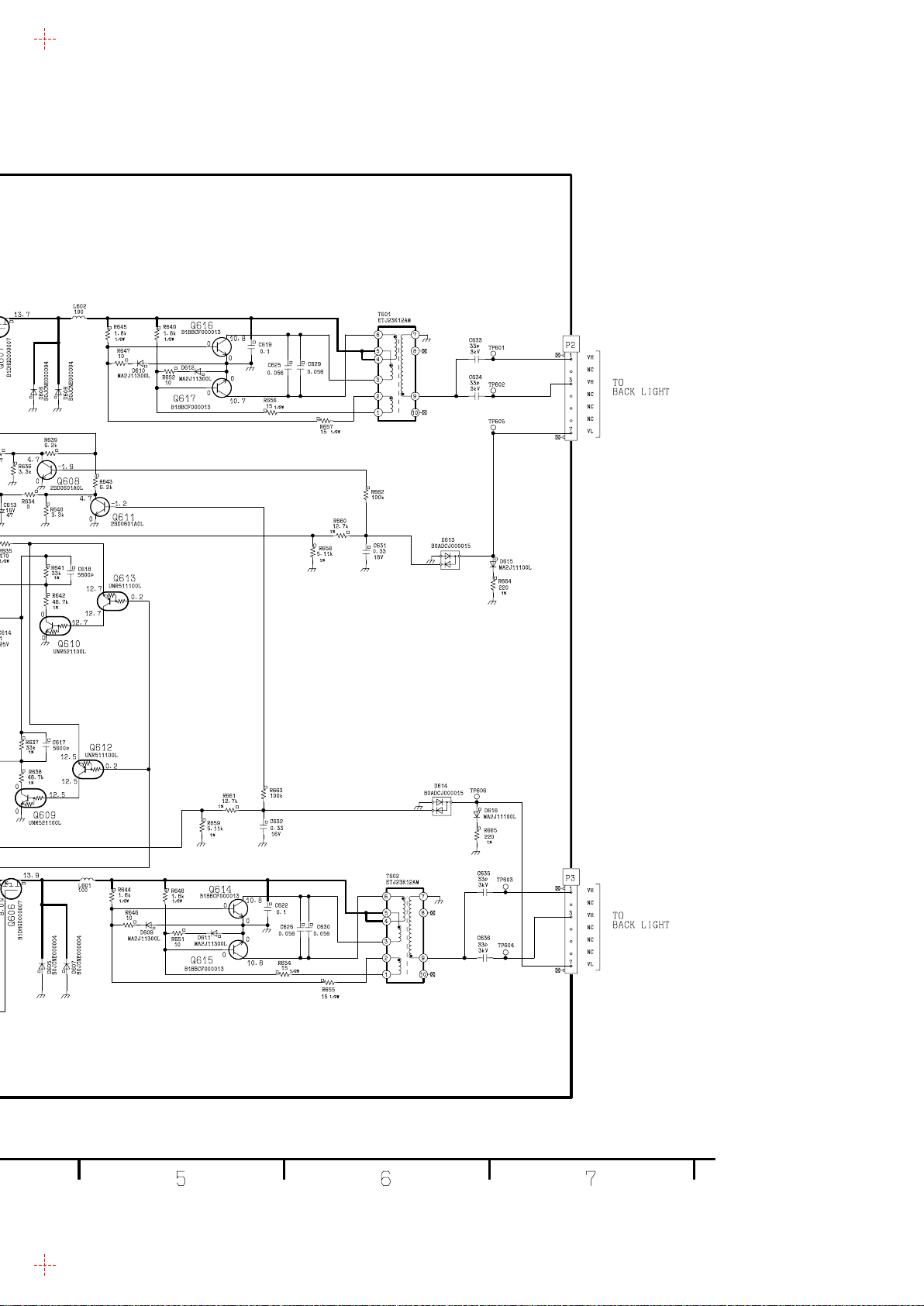
11.14. P-Board Schematic Diagram
TX-15LT2M/Q/T/X/Z
P-Board Schematic Diagram
44
Page 75
44
TX-15LT2M/Q/T/X/Z
P-Board Schematic Diagram
Page 76
M Q Z X T
b0
Colour system
b1b2b3b4TV NTSC 50
b5
TV SECAM 60
b6
AV NTSC 50
b7
AV SECAM 60
b0
CH Plan
ASIA / M.E. / HK / UK / CHINA (1)
b1
NZ / INDES (1)
b2
AUSTRALIA (1)
b3
E. EUROPE (1)
b4
SPECIAL (1)
b5
AMERICA (1)
b6
CATV (1)
b7
JAPAN (1)
b0
sub picture
b1
2tuner
b2
VGAb3YUVb4Wide (16:9)
b5
HYPER
b6
SIF
I only(0), BG only(1)
b7
I/BG/DK/L(2), BG/DK(3)
b0
A2 enable
4.5 (1)
b1
5.5 (1)
b2
6.0 (1)
b3
6.5 (1)
b4
NICAM enable
4.5 (1)
b5
5.5 (1)
b6
6.0 (1)
b7
6.5 (1)
b0
A2 select 6.5MHz
5.742 MHz (0), 6.742 MHz
b1
NICAM priority
ASIA / M.E. (1)
b2
HK / UK (1)
b3
CHINA (1)
b4
NZ / INDN (1)
b5
AUSTRALIA (1)
b6
E. EUROPE (1)
b7
SPECIAL (1)
b0
VCR/GAME in search
b1
SASO enable
b2
Noise mute
b3
Monitor out AV1 mute
b4
AV SW 3/2AV out
b5
Tunerb6Child lock
Child lock enable (1)
b7
TEXT VDEFEAT
VDEFEAT ON (1), OFF (0)
b0
Power up EC-Mode
b1
CH Blanking
b2
AV Blanking
b3
Auto WIDE
b4
Volume correction
b5
AVLink
b6
MPX/NICAM display
b7
free
1
Option Models
option1
Auto(1)
SECAM(1)
NTSC(1)
M.NTSC(1)
Reserved
Reserved
Reserved
Reserved
without sub-picture (0), with sub-picture (1)
2 tuner (1), 1 tuner (0)
enable (1)
enable (1)
16:9 (1), 4:3 (0)
not use
On (0), Off (1)
SASO enable (1)
Noise mute enable(0)
Monitor out AV1 mute(1)
set to 0
MACO tuner (0), ALPS tuner (1)
Power on EC enable (1)
Blanking enable (1)
Blanking enable (1)
WSS enable only in aspect Auto (0), WSS always enable (1)
TV Volume correction enable (1)
Q-Link on/off selectable in menu (1)
Display NICAM (0), Display MPX (1)
option2
1
option3
1
1
0
option7
option6
1
option5
option4
0
Description
CF
1
1
1
1
0
0
1
FF
1
1
1
1
1
1
1
10
0
0
0
0
1
0
0
E2
0
1
0
0
0
1
1
DE
0
1
1
1
1
0
1
C1
1
0
0
0
0
0
1
46
0
1
1
0
0
0
1
Page 77
M Q Z X T
Option Models
Description
b0
Teletext CH Refresh
b1
Geomagnetic Sensor
b2
Geomagnetic Polarity
b3
RF Attenuation
b4
Fine tuning
b5
Search speed
b6
TEXT FLOF
b7
TEXT TOP
b0
freeb1freeb2freeb3freeb4freeb5Surround SP polarity
b6
Volume curve
b7
Volume EXDAC
b011
OSD language
English Only enable (1) : Top Prority
b110b201b300b400Blue Back
b500
freeb600freeb711OVPb0Shop mode
b1
Full / 16:9 display
Reserved
b2
Sub Headphone
b3
Scan mode Blanking
b4
User aspect 14:9
b5
NICAM C4 bit
b6
ID-1b71080i
b0
Asia
b1
Australia
Australia (1)
b2
Ireland
Ireland(1)
b3
UK
UK(1)
b4
MELCOA
MELCOA (1)
b5
28 inch
b6
Large size
b7
PTVb0VDU Version
b1
GC Version
b2
UV Swap
b3
TEXTb4LT2 22inch
b5
freeb6Picture Shift
set to 1
b7
CIP2
22inch (1), 15inch (0)
Asia (1), europe (0)
Reserved for 28 inch etc.
set to 1
set to 0
enable (1)
enable (1)
enable (1)
without CIP1 (0), with CIP (1)
A21 (0), A12(1)
ES5 (0), ES6 (1)
Swap (1)
Enable (1)
enable (1)
Blanking enable (1)
set to 1
set to 0
Volume curve1(0), curve2(1)
Add Volume
Arabic enable (1)
Russian enable (1)
Chinese enable (1)
enable(0)
enable (1)
enable(1)
set to 0
Reserved
set to 0
Enable(1)
Enable(1)
Slow(1) Fast(0)
TOP enable (1)
0
option9
option8
option13
option12
option11
option10
1
1001000
1
0
1
Enable(1)
0
51 D0
1 0
0 0
0 0
0 0
1 1
0 0
1 1
0 1
51
1
0
0
0
1
0
1
80
0
0
0
0
0
0
0
83 85
89
0A
0
0
0
1
0
1
0
41 43
1 1
0 1
0 0
0 0
0 0
0 0
1 1
0 0
4A
0
1
0
1
0
0
1
41
1
0
0
0
0
0
1
Area Option
Temporary
Page 78
Important Safety Notice
Components identified by mark have special characteristics important for safety.
When replacing any of these components, use only manufacture's specified parts.
Notes:
1. Resistor
All resistors are cabon 1/4W resistor, unless marked as follows:
Unit of resistance is OHM [W] (K=1,000, M=1,000,000).
: Nonflammable : Metal Oxide
: Solid : Metal Film
: Wire Wound : Fuse:
2. Capacitor
All capacitors are ceramic 50V capacitor, unless marked as follows:
Unit of capacitance is mF, unless otherwise noted.
: Temperature Compensation : Electrolytic
: Polyester : Bipolar
M
m T
: Metalized Polyester : Dipped Tantalum
: Polypropylene : Z-Type
3. Coil
Unit of inductance is mF, unless otherwise noted.
4. Test Point
: Test Point position
5. Earth Symbol
: Chassis Earth (Cold) : Line Earth (Hot)
6. Voltage Measurement
Voltage is measured by a DC voltmeter.
Conditions of the measurement are the following:
Power Source ................................................... AC 100-240V, 50/60Hz
Receiving Signal ............................................... Colour Bar signal (RF)
All customer's controls ...................................... Maximum positions
7. Number in red circle indicates waveform nember.
(See waveform pattern table.)
8. When arrow mark ( ) is found, connection is easily found from the direction of arrow
NP
+
-
Z
9. Indicates the major signal flow. : Video Audio
10. This schematic diagram is the latest at the time of printing and subject to change without
notice.
TX-15LT2M/Q/T/X/Z
Schematic Diagram Notes
Page 79
TX-15LT2M/Q/T/X/Z Power Block Diagram TX-15LT2M/Q/T/X/Z Power Block Diagram
Page 80
Page 81
Page 82
Page 83
Page 84
Page 85
Page 86
Page 87
Page 88
Page 89
Page 90
Page 91
Page 92
Page 93
Page 94
Page 95
Page 96
Page 97
Page 98
Page 99
Page 100
 Loading...