

Panasonic TH-50PV60L Service manual

Plasma Television
A
A
V
t
A
TH-50PV60L
GP9DE Chassis
ORDER NO.ITD0604014AE
Please file and use this manual together with the service manual for Model No.TH-50PV60A, Order
No.ITD0604008CE.
Power Source
Power Consumption
Averageuse 461 W
Standbycondition 0.3 W
Plasma Displaypanel
Drive method
AspectRatio 16:9
Contrast Ratio Max10000:1
isible screen size 127 cmV
(No. ofpixels) 1,106 mm (W) × 622 mm (H) × 1,269 mm (diagonal)
Sound
Speaker 12 cm × 6 cm × 2 pcs, 8 Ω
AudioOutpu
Headphones M3 (3.5 mm) Jack × 1
PC signals VGA, SVGA, XG
C 110-220 V, 50/60 Hz
C type
1,049,088 (1,366 (W) × 768 (H)) [4,098 × 768 dots]
20 W [10 W + 10 W] (10 % THD)
SXGA.....(compressed)
Horizontal scanning frequency 31-69 kHz
Vertical scanning frequency 59-86 Hz
© 2006 Matsushita Electric Industrial Co., Ltd. All
rights reserved. Unauthorized copying and
distribution is a violation of law.
/
V
V
y
V
V
Y
V
Y
4
V
t
t
t
r
V
t
TH-50PV60L
Receiving Systems
Band Name
Receiving Channels
(Regular TV) 2-13 (NTSC M USA) 14-69 (NTSC M USA) 1-125 (USA CATV)
Aerial - Rear VHF / UHF
Operating Conditions
Temperature 0 °C - 40 °C
Humidit
Connection Terminals
AV1
Input
AV2
Input
AV3
Input
AV
Input
Others HDMI1/2 Inpu
Monito
Output
Dimensions (W×H×D) 1,210 mm × 818 mm × 95 mm
Weigh
AUDIOL-R RCA PIN Type × 2 0.5 V[rms]
IDEO RCA PIN Type × 1 1.0 V[p-p] (75 Ω)
SVIDEO Mini DIN 4-pin Y: 1.0 V[p-p] (75 Ω) C: 0.286 V[p-p] (75 Ω)
AUDIOL-R RCA PIN Type × 2 0.5 V[rms]
IDEO RCA PIN Type × 1 1.0 V[p-p] (75 Ω)
COMPONENT
AUDIOL-R RCA PIN Type × 2 0.5 V[rms]
IDEO RCA PIN Type × 1 1.0 V[p-p] (75 Ω)
COMPONENT
AUDIOL-R RCA PIN Type × 2 0.5 V[rms]
IDEO RCA PIN Type × 1 1.0 V[p-p] (75 Ω)
SVIDEO Mini DIN 4-pin Y: 1.0 V[p-p] (75 Ω) C: 0.286 V[p-p] (75 Ω)
PC Inpu
AudioInpu
AUDIOL-R RCA PIN Type × 2 0.5 V[rms] (high impedance)
IDEO RCA PIN Type × 1 1.0 V[p-p] (75 Ω)
HF BAND UHF BAND CAT
20% - 80 % RH (non-condensing)
1.0 V[p-p] (including synchronization)
PB/CB,PR/C
PB/CB,PR/C
TYPEAConnectors
HIGH-DENSITYD-SUB 15 PIN R, G, B/0.7 V[p-p] (75 Ω)
RCA PIN Type × 2 0.5 V[rms]
(TV Set only)
40.0 kg Net (TV Set only) 42.5 kg Net (With Pedestal)
R
R
± 0.35 V[p-p]
1.0 V[p-p] (including synchronization)
± 0.35 V[p-p]
HD, VD/TTL Level 2.0-5.0 V[p-p] (high impedance)
1,210 mm × 882 mm × 371 mm
(With Pedestal)
Note:
Design and Specifications are subject change without notice.
Weight and Dimensions shown are approximate.
CONTENTS
Page Page
1 Difference PCB Structure sheet 4
2 Service Mode Function
2.1. How to enter SERVICE 1
2.2. How to enter SERVICE 2
2.3. Option Description
3 Adjustment
3.1. PAL panel white balance adjustment
5
5
5
7
9
9
3.2. HD white balance adjustment
3.3. Sub bright adjustment
3.4. ABL adjustment
3.5. Sub-Contrast adjustment
4 Conductor Views
4.1. TU-Board
4.2. DG-Board
2
10
11
12
13
15
15
16
5 Block and Schematic Diagram 19
5.1. Schematic Diagram Note
5.2. Main Block Diagram
5.3. TU-Board Block and Schematic Diagram
5.4. DG-Board (1 of 3) Block Diagram
5.5. DG-Board (2 of 3) Block Diagram
5.6. DG-Board (3 of 3) Block Diagram
5.7. DG-Board (1 of 8) Schematic Diagram
5.8. DG-Board (2 of 8) Schematic Diagram
5.9. DG-Board (3 of 8) Schematic Diagram
5.10. DG-Board (4 of 8) Schematic Diagram
5.11. DG-Board (5 of 8) Schematic Diagram
5.12. DG-Board (6 of 8) Schematic Diagram
5.13. DG-Board (7 of 8) Schematic Diagram
19
20
21
22
23
24
25
26
27
28
29
30
31
5.14. DG-Board (8 of 8) Schematic Diagram
6 Parts Location & Mechanical Replacement Parts List
6.1. Parts Location
6.2. Packing Exploded Views (1)
6.3. Packing Exploded Views (2)
6.4. Packing Exploded Views
6.5. Stand Exploded Views
6.6. Mechanical Replacement Parts List (PDP TV)
6.7. Mechanical Replacement Parts List (Stand)
7 Electrical Replacement Parts List
7.1. Replacement Parts List Notes
7.2. Electrical Replacement Parts List
8 Schematic Diagram for printing with A4
TH-50PV60L
32
33
33
34
35
36
37
38
39
40
40
41
67
3
TH-50PV60L
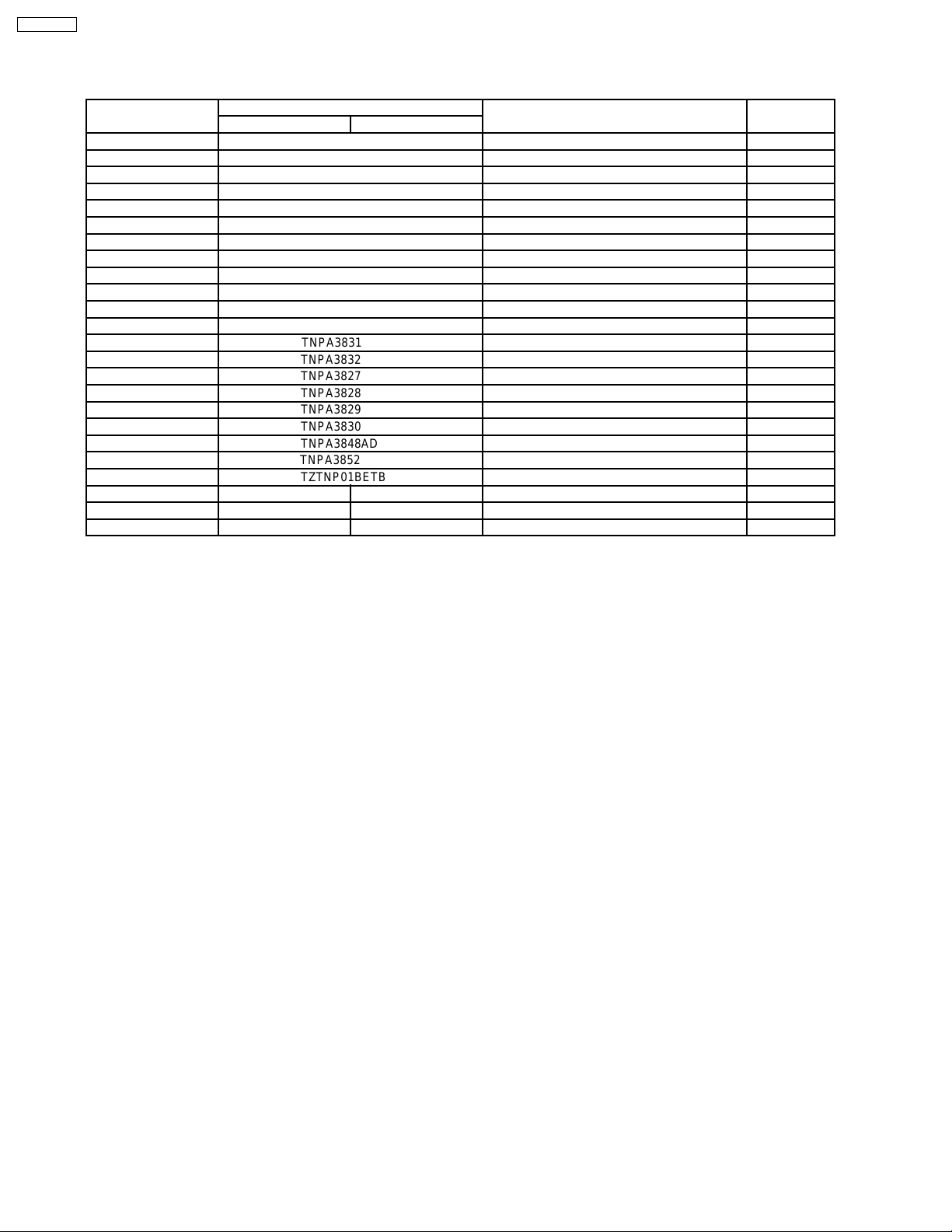
1 Difference PCB Structure sheet
Print List
Board name Part No. Function Remarks
TH-50PV60A TH-50PV60L
P ETXMM610MEF Power Supply
H TNPA3760AD AV Terminal, AV switch
PA TNPA3761AC DC-DC Converter, Power SOS
K TNPA3762AE Remote receiver, LED, Keyscan
S TNPA3763AC Power Switch
G TNPA3764AF Front terminal
C1 TNPA3821 Data Draiver (Up Left)
C2 TNPA3822 Data Draiver (Up Middle)
C3 TNPA3823 Data Draiver (Up Right)
C4 TNPA3824 Data Draiver (Down Right)
C5 TNPA3825 Data Draiver (Down Middle)
C6 TNPA3826 Data Draiver (Down Left)
SU TNPA3831 Scan Out (Upper)
SD TNPA3832 Scan Out (Lower)
SC TNPA3827 Scan Drive
SS TNPA3828 Sustain Drive
SS2 TNPA3829 Sustain Connector (Up)
SS3 TNPA3830 Sustain Connector (Down)
GK TNPA3848AD Key Switch
HC TNPA3852 JIG Connection
D TZTNP01BETB Format Converter, Plasma AI Processor
DG TNPA3756CP TNPA3756CX Digital Signal Processor Changed
TA TNPA3768AC ----- Tuner Deleted
TU ----- TNPA3851 Tuner Added
4

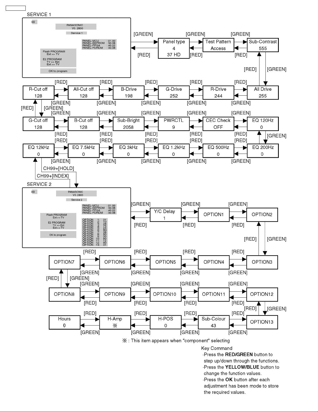
2 Service Mode Function
MPU controls the functions switching for each IICs through IIC bus in this chassis. The following setting and adjustment can be
adjusted by remote control in Service Mode.
2.1. How to enter SERVICE 1
1. In sound menu, set BASS to MAXIMUM, and set TREBLE to MINIMUM.
2. Set the Volume to minimum and set the off timer.
3. Simultaneously press Recall button on remote control and DOWN button [
2.2. How to enter SERVICE 2
1. Set the channel to CH99.
2. Select the EQ 12kHz.
3. Press Mute button on remote control and DOWN button [
Note:
To exit to Service mode, press EXIT or Power button on remote control.
] on the TV set.
] on the TV set.
TH-50PV60L
5
TH-50PV60L
6
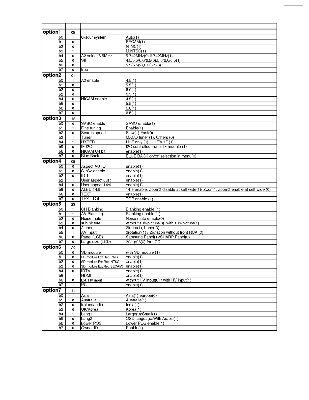
2.3. Option Description
TH-50PV60L
7
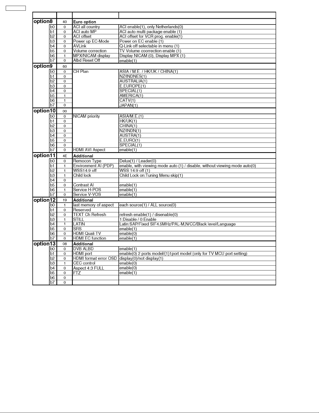
TH-50PV60L
8
3 Adjustment
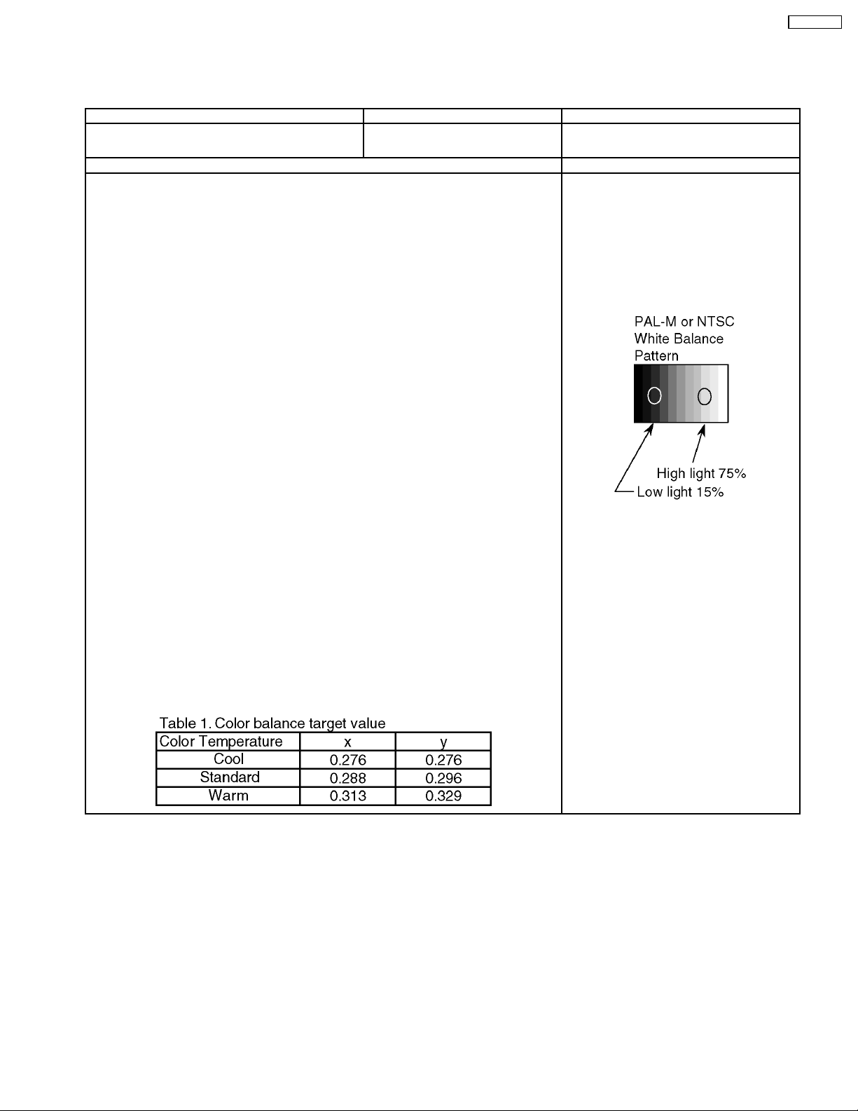
3.1. PAL panel white balance adjustment
Instrument Name Connection Remarks
· W/B pattern (PAL-M or NTSC signal)
· Color analyzer (Minolta CA-100 or equivalent)
Procedure Remarks
· Asing time is longer than 15min.
· Make sure the front panel to be used on the final set is fitted.
· Make sure a color signal is not being shown before adjustment.
· Put the color analyzer where there is little colour variation.
Complete the adjustment within 10 minutes after the turn on electricity.
Turn on the power supply again when it is not possible to complete it by aging etc.
1. Display the white balance pattern.
2. Check that the color balance is “cool”.
3. Enter the <Service1> mode.
4. Select “G-CUTOFF” item, using the color-key “Red” or “Green”, and set to “128”, using the
color-key “Yellow” or “Blue”.
Also, “B-CUTOFF” and “R-CUTOFF” set to “128”.
5. Set “G-DRIVE” at “208”.
6. Touch the signal receiver of color analyzer to the highlight window’s center, and adjust B
drive and R drive so x, y become the “Color balance Cool” in the below table.
7. Set “ALL-DRIVE” to “252”.
8. Set colorbalance to “STANDARD”.
9. Fix G cutoff , B cutoff and R cutoff at “128”.
10. Fix G drive at “208”.
11. Adjust B drive and R drive so the highlight window’s x, y become the “Color balance
“STANDARD” in the below table.
12. Set “ALL-DRIVE” to “252”.
13. Set color balance to “Warm”.
14. Set G cutoff, B cutoff and R cutoff to “128”.
15. Set G drive to “208”.
16. Adjust B drive and R drive so the highlight window’s x, y become the “Color balance Warm”
shown in the below table.
17. Set “ALL-DRIVE” to “252”.
RF input
Panel surface
TH-50PV60L
User setting: Normal
Picture menu : Dynamic
ASPECT : 16:9
· Highlight section
Signal amplitude 75%
9
TH-50PV60L
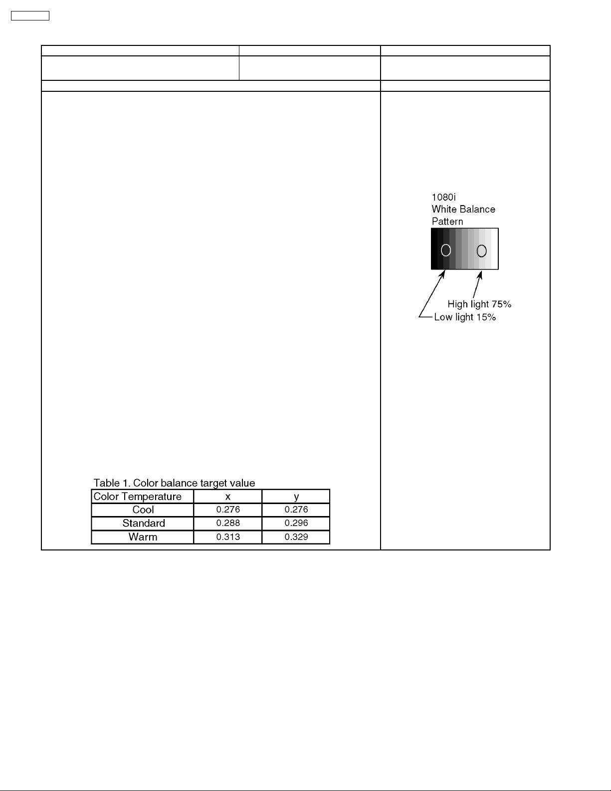
3.2. HD white balance adjustment
Instrument Name Connection Remarks
· 1080i W/B Pattern
· Color analyzer(Minolta CA-100 or equivalent)
Procedure Remarks
· Asing time is longer than 15min.
· Make sure the front panel to be used on the final set is fitted.
· Make sure a color signal is not being shown before adjustment.
· Put the color analyzer where there is little colour variation.
· Complete the adjustment within 10 minutes after the turn on electricity.
Turn on the power supply again when it is not possible to complete it by aging etc.
1. Display the white balance pattern.
2. Check that the color balance is “cool”.
3. Enter the <Service1> mode.
4. Select “G-CUTOFF” item, using the color-key “Red” or “Green”, and set to “128”, using the
color-key “Yellow” or “Blue”.
Also, “B-CUTOFF” and “R-CUTOFF” set to “128”.
5. Set “G-DRIVE” at “208”.
6. Touch the signal receiver of color analyzer to the highlight window’s center, and adjust B
drive and R drive so x, y become the “Color balance Cool” in the below table.
7. Set “ALL-DRIVE” to “252”.
8. Set colorbalance to “Standard”.
9. Fix G cutoff , B cutoff and R cutoff at “128”.
10. Fix G drive at “208”.
11. Adjust B drive and R drive so the highlight window’s x, y become the “Color balance
“Standard” in the below table.
12. Set “ALL-DRIVE” to “252”.
13. Set color balance to “Warm”.
14. Set G cutoff, B cutoff and R cutoff to “128”.
15. Set G drive to “208”.
16. Adjust B drive and R drive so the highlight window’s x, y become the “Color balance Warm”
shown in the below table.
17. Set “ALL-DRIVE” to “252”.
· RF input
· Panel surface
User setting: Normal
Picture menu: Dynamic
ASPECT:16:9
· Highlight section
Signal amplitude 75%
* The Color balance COOL differs from
Japanese model values.
10
3.3. Sub bright adjustment
Instrument Name Connection Remarks
1. PAL-M or NTSC signal generator (or RF) Connect to the input terminal User setting: Normal
Procedure Remarks
· White balance adjustment is finished for each signal.
· Do adjustments in a dark room.
· Complete the adjustment within 10 minutes after the turn on electricity.
Turn on the power supply again when it is not possible to complete it by aging etc.
1. Display the 10 steps gray-scale pattern for adjusting subbright from video input.
2. Use "Sub-Bright" in the <Sevice1> mode to adjust so the 6th section shows up and the
7th fades away.
Data
Sub-Bright data addresses
Sub-Bright (upper) A0-0116
Sub-Bright (lower) A0-0117
Picture menu: Dynamic
Color balance: Normal
ASPECT: 16:9
TH-50PV60L
11
TH-50PV60L
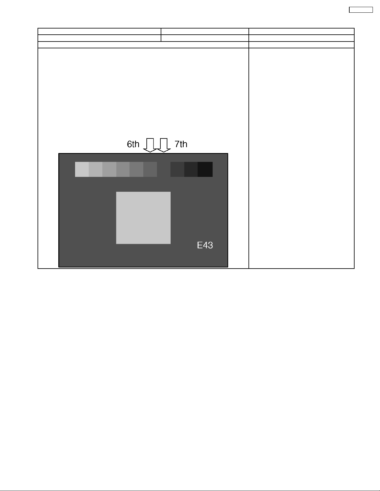
3.4. ABL adjustment
Instrument Name Connection Remarks
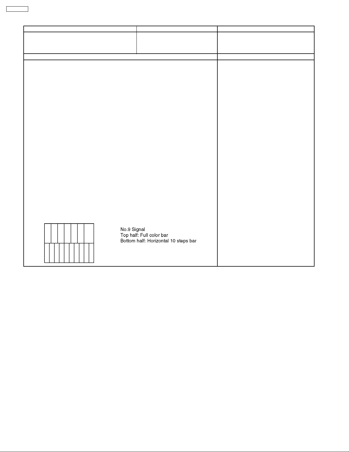
1. HD signal emitter (or Leader : 1080i/No.9 signal)
2. Wattmeter
· Make sure the set is aged for 30 minutes or more before adjustment.
(Do not switch off during or after aging.)
· Voltage 230V 50Hz (variation within 1%)
· Volume at minimum and screen size at “16:9”
Component input, dynamic, standard
1. Connect the set´s AC power to the wattmeter.
2. Input the signal (top half: color bar, Bottom half :Horizontal 10steps bar).
3. Select the “PWRCTL” item in the <Service1> mode.
4. Adjust PWRCTL so the set´s power consumption is
438 ±10W
Remarks
1. The initial data are
Data address: A0-0102
Default data: 0x00
2. The power and data are in reverse relationship.
(Lower the data to raise the power.)
· Raising direction (↑): 0→255, 254, 253
· Lowering direction (↓): 0→1, 2, 3
3. There is a possibility that the adjustment value can do two places, adjust it in that case, that
the value of PWRCTL is large.
COMPONENT input terminal
Connect the AC power of the set to the
wattmeter.
Procedure Remarks
12
3.5. Sub-Contrast adjustment
Name of measuring instrument Connection Remarks
RF generator
Base Band generator
Preparation (AV) Remarks
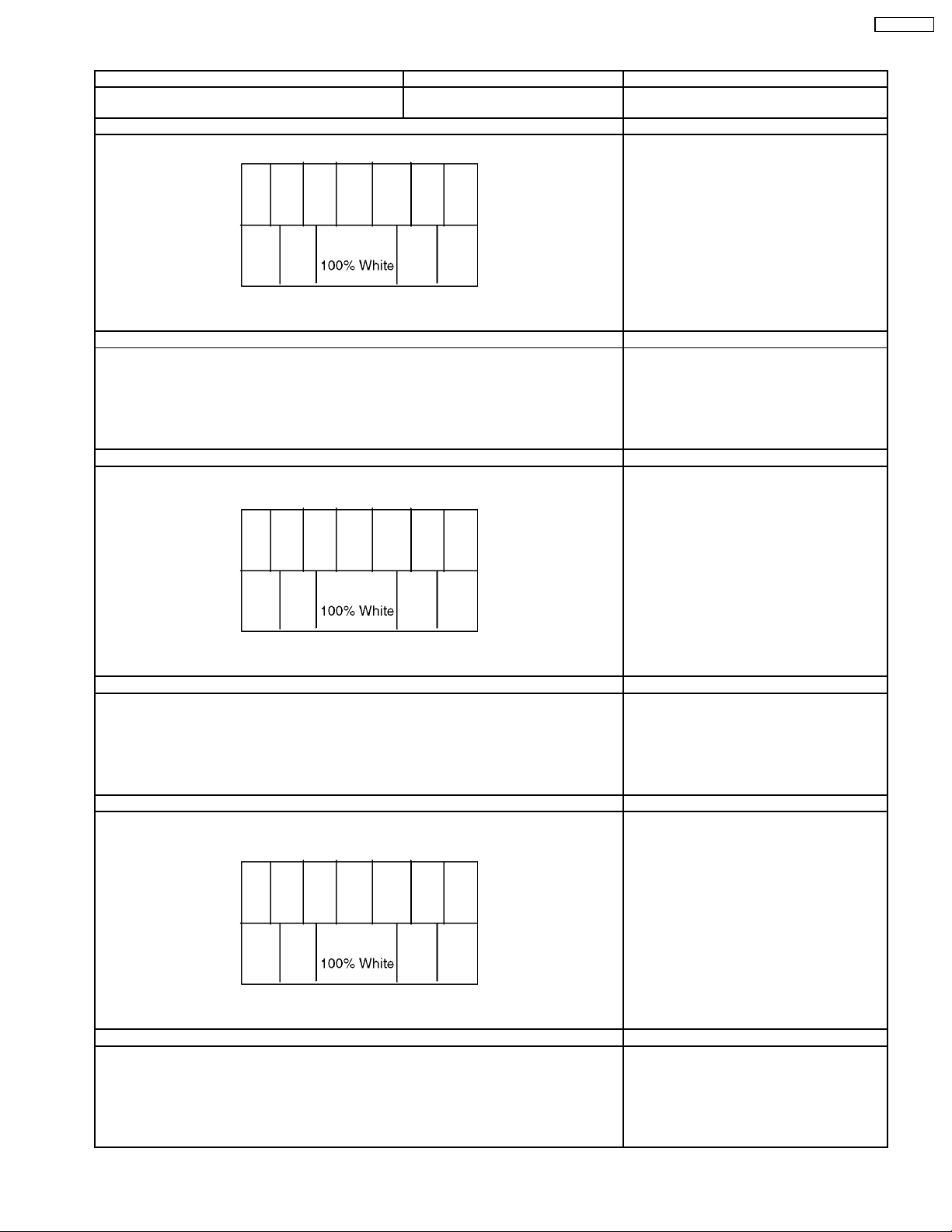
1. Receive AV1 (PAL-M or NTSC 100% Full White or Split Colour bar shown as below) .
2. Goes into service mode, choose Sub-Contrast, and it checks that data value is 512.
(It checks that an initial value is a default)
Adjustment of AV system Remarks
1. The colour key yellow button of remote control is pushed.
2. The OSD character of sub-contrast becomes red.
(Inside under automatic adjustment)
3. The OSD character of sub-contrast returns to white.
4. End.
Preparation (RF) Remarks
1. Receive a RF E-21 ch (PAL-M or NTSC 100% Full White or Split Colour bar shown as
below.)
TH-50PV60L
2. Goes into service mode, choose Sub-Contrast, and it checks that data value is 512.
(It checks that an initial value is a default)
Adjustment of RF system Remarks
1. The colour key yellow button of remote control is pushed.
2. The OSD character of sub-contrast becomes red.
(Inside under automatic adjustment)
3. The OSD character of sub-contrast returns to white.
4. End.
Preparation (HD) Remarks
1. Receive Component
(1080i/ 60Hz or 1080i/ 50Hz, 100% Full White or Split colour bar as shown below.)
2. Goes into service mode, choose Sub-Contrast, and it checks that data value is 384.
(It checks that an initial value is a default)
Adjustment of HD system Remarks
1. The colour key yellow button of remote control is pushed.
2. The OSD character of sub-contrast becomes red.
(Inside under automatic adjustment)
3. The OSD character of sub-contrast returns to white.
4. End.
13

TH-50PV60L
14
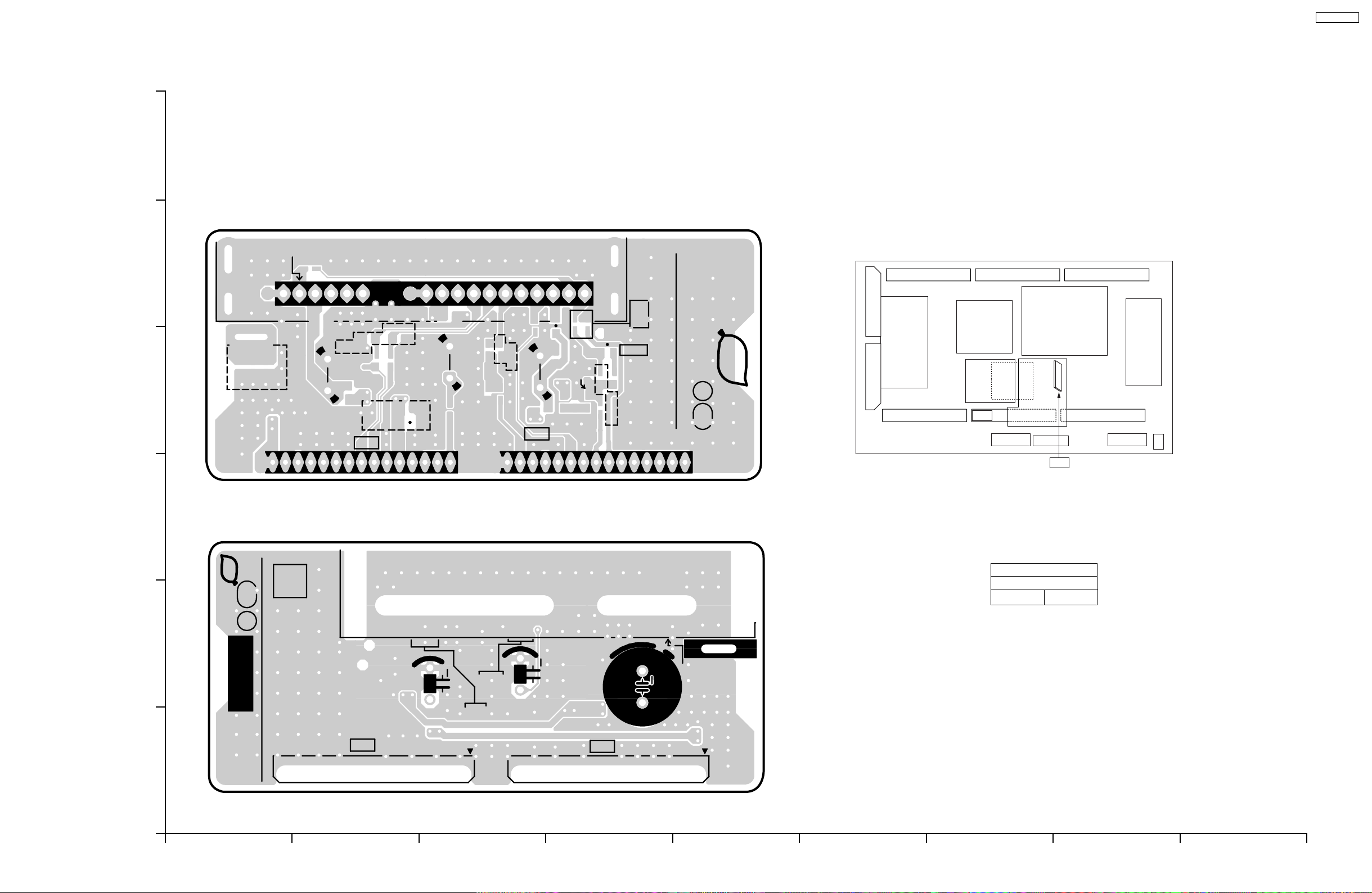
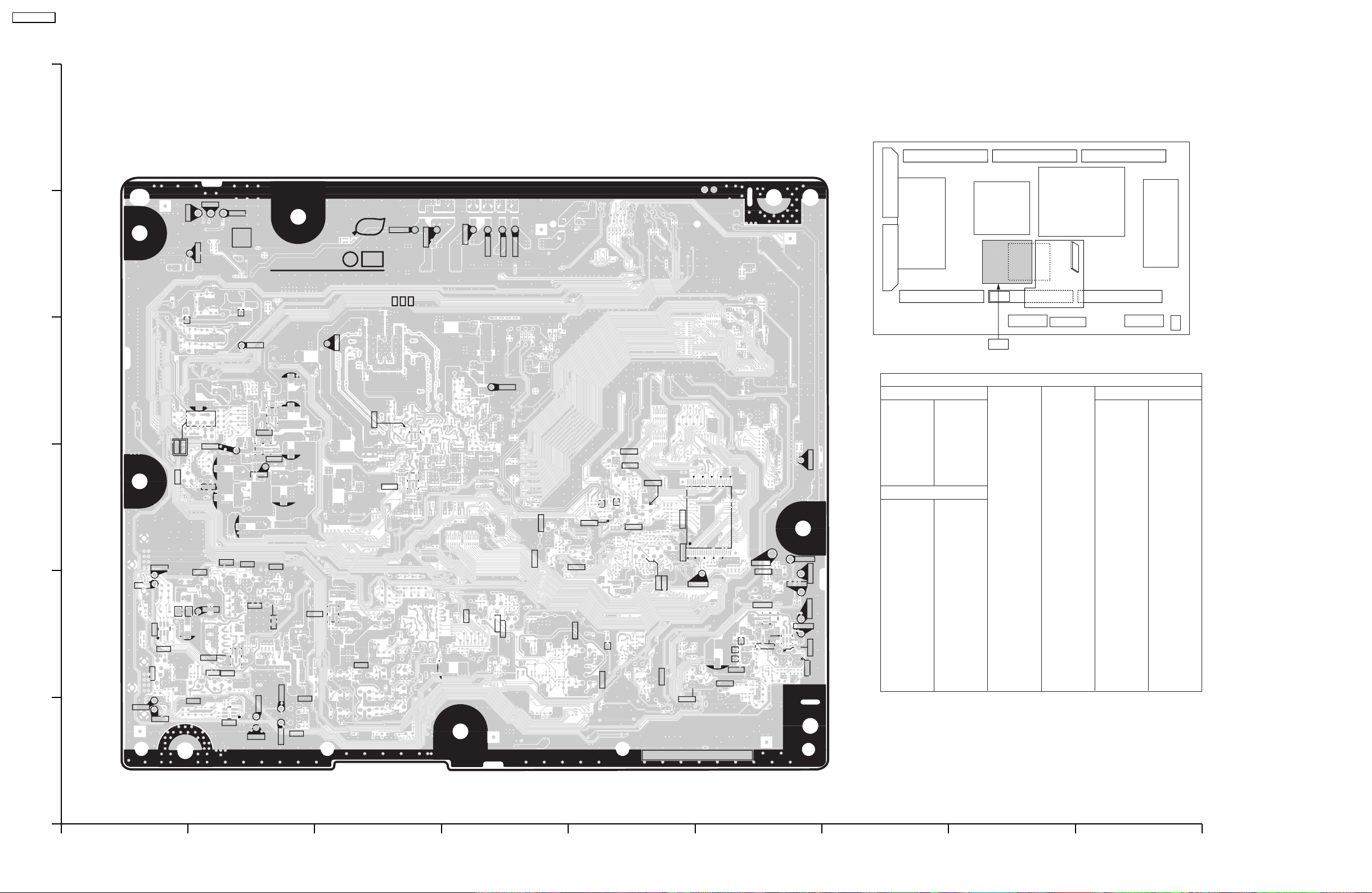
4 Conductor Views
4.1. TU-Board
6
TU-BOARD (FOIL SIDE)
TNPA3851
AGCADJ
JS010
JS003
+B
C021
C007
C001
5
JS016
4
115
C019
L018
TU001
C017
TU5
R012
C023
C018
R013
BT
C013
C002
L017
AGC
IFOUT
R014
AGCCONT
SCL
SDA
C020
AFT
L021
L012
R016
SIFOUT
C003
L008
TU6
BTL
R011
C009
R005
L022
C016
VIDEOOUT
JS002
R008
Q002
R015
R009
R002
TNPA3851
SEE REVERSE FOR ORDER NO.
PbF
1
TU
115
TH-50PV60L
TU
3
TU-BOARD (COMPONENT SIDE)
TNPA3851
Parts Location
PbF
TU
TU-BOARD
TRANSISTOR
Q002 D-4
1
2
NO.
ORDER
1
TU001
VIDEOOUT
TU6
AGCCONT
C003
BT
AFT
SDA
SCLIFOUT
AGC
BTL
SIFOUT
115
C002
15
C001
TU5
+B
AGCADJ
1
TNPA3851
TH-50PV60L TU-BOARD TNPA3851 TH-50PV60L TU-BOARD TNPA3851
A
C E GIBDFH
15
TH-50PV60L
4.2. DG-Board
6
DG-BOARD (FOIL SIDE)
TNPA3756CX
TP038
TP039
TP040
TP1117
TP1113
PbF
TP1114
5
TNPA3756 DG
1
SEE REVERSE FOR SUFFIX
CR NO.4
IC017
TP041
+
IC029
1
+
+
1
Q045
IC030
1
TP028
4
1
TP029
IC018
IC016
1
Q053
Q078
Q055
TP030
Q079
3
Q075
Q073
Q076
Q074
Q067
TP031
TP033
Q071
Q068
TP066
2
Q066
Q065
TP034
TP032
Q077
IC024
Q082
Q083
Q070
1
TP035
TP064
TP065
TP036
Q084
Q069
TP1119
+
Q061
+
TP1118
Q1138
TP1116
TP037
Q1122
TP1115
Q1118
Q1117
Q1120
Q1134
Q1103
Q1135
Q1139
Q1101
Q1100
Q1102
Q918
Q1107
Q919
48
IC1101
Q1125
Q1106
1
TP1106
Q1112
Q1111
DG
Parts Location
DG-BOARD (FOIL SIDE)
IC
IC1101 E-3
IC1104 F-2
IC1110 F-2
IC4016 B-3
TP1120
25
IC4017 B-2
IC4018 B-4
IC4024 B-2
IC4029 C-4
IC4030 C-3
TRANSISTOR
Q1100 E-3
Q1101 E-3
Q1102 E-3
Q1103 E-3
Q1106 E-1
24
TP1101
Q1137
IC1110
IC1104
TP1102
TP1104
TP1103
1
TP1105
TP1107
Q1140
1
Q1141
Q1107 E-2
Q1111 F-2
Q1112 F-2
Q1117 D-3
Q1118 D-3
Q1120 E-3
Q1122 D-2
Q1125 E-3
Q1134 E-2
Q1135 E-2
Q1137 F-2
Q1138 D-2
Q1139 E-3
Q1140 F-2
Q1141 F-2
Q4045 C-2
Q4053 A-3
Q4055 A-3
Q4061 D-2
Q4065 A-2
Q4066 A-2
Q4067 B-2
Q4068 B-2
Q4069 B-1
Q4070 B-1
Q4071 A-2
Q4073 B-3
Q4074 B-2
Q4075 B-3
Q4076 B-3
Q4077 B-1
Q4078 A-3
Q4079 B-3
Q4082 B-2
Q4083 B-2
Q4084 B-1
Q4918 E-2
Q4919 E-2
TP
TP1101 F-3
TP1102 F-3
TP1103 F-2
TP1104 F-2
TP1105 F-2
TP1106 F-2
TP1107 F-2
TP1113 C-5
TP1114 B-5
TP1115 D-5
TP1116 D-5
TP1117 C-5
TP1118 D-5
TP1119 D-5
TP1120 F-3
TP4028 B-4
TP4029 B-3
TP4030 B-3
TP4031 A-2
TP4032 A-4
TP4033 A-3
TP4034 A-1
TP4035 B-1
TP4036 B-1
TP4037 D-4
TP4038 B-5
TP4039 B-5
TP4040 B-5
TP4041 C-4
TP4064 B-1
TP4065 B-1
TP4066 B-2
1
TH-50PV60L
DG-BOARD TNPA3756CX
ABCDEFGH I
TH-50PV60L
DG-BOARD TNPA3756CX
16

TH-50PV60L
6
DG-BOARD (COMPONENT SIDE)
TNPA3756CX
55
17
56
DG35
1
1
1
1
21
32
1
DG3
40
1
58
TP1109
PbF
Q1114
Q1108
Q1116
1
1
IC1105
64
IC036
49
48
27
28
54
55
IC1103
108
109
Q1109
Q1110
7
8
1
14
DG15
Q1104
1
IC1100
54
1
216
163
162
NP
Q1105
814
NP
IC1106
7
1
40
Q1143
DG7
16
17
33
Q1113
5
DG5
4
TP1108
3
4
IC1102
IC1111
2
1
Q1115
1
DG22
DG20
40
110
THERMAL PAD
IC032
1
8
TNPA3756
5
Q1130
4
IC034
IC037
IC020
1
8
25
Q062
Q063
1
IC040
A
100
26
Q064
1
IC014
Q051
1
4
IC039
58
Q1121
Q1132
Q1133
Q1142
19
20
18
16
9
14
1
7
IC1107
Q1131
1
2
1
SUFFIX
DADBDCDDDEDFDGDHDJDKDLDMDNDPDQDRDSDTDUDVDW
1
1
76
Q054
Q052
DG2
CACBCCCDCECFCG
75
50
CRNO.4
A
51
CHCJCKCLCMCNCP
Q060
Q046
Q044
Q043
Q040
Q042
Q041
151
DG
1
IC038
IC027
CQCRCSCTCUCVCWCXCY
8
1
100
1
25
26
4
1
THERMAL PAD
IC013
58
108
109
144
1
1
DX
5
IC035
4
THERMAL PAD
IC028
+
1
4
16
1
IC025
76
50
8
1
8
1
IC033
75
51
NP
8
5
9
8
73
36
14
DG10
7
45
Q059
Q058
Q057
Q056
IC019
NP
72
THERMAL PAD
IC026
IC022
37
5
IC023
Q081
Q080
80
Q050
DG
DG1
1
DG8
19 1
8
5
4
1
DG9
1
19
Parts Location
IC
IC1100 C-4
IC1102 A-2
IC1103 B-3
IC1105 B-2
IC1106 C-2
IC1107 D-2
IC1111 A-2
IC4013 E-3
IC4014 D-1
IC4019 F-4
IC4020 D-3
IC4022 F-2
IC4023 F-1
IC4025 F-3
IC4026 F-2
IC4027 E-1
IC4028 F-3
IC4032 D-5
IC4033 F-5
IC4034 D-4
IC4035 E-4
IC4036 B-4
IC4037 D-4
IC4038 E-4
IC4039 C-4
IC4040 D-2
DG-BOARD (COMPONENT SIDE)
TRANSISTOR
Q1104 B-2
Q1105 C-2
Q1108 B-2
Q1109 B-2
Q1110 B-2
Q1113 A-2
Q1114 B-2
Q1115 A-2
Q1116 B-2
Q1121 C-2
Q1130 D-2
Q1131 D-2
Q1132 C-2
Q1133 C-2
Q1142 C-1
Q1143 C-1
Q4040 E-2
Q4041 E-1
Q4042 E-2
Q4043 E-2
Q4044 E-2
Q4046 E-2
Q4050 F-5
Q4051 D-1
Q4052 D-2
Q4054 D-2
Q4056 F-4
Q4057 F-4
Q4058 F-4
Q4059 F-5
Q4060 E-2
Q4062 D-2
Q4063 D-2
Q4064 D-2
Q4080 F-4
Q4081 F-4
TP
TP1108 A-4
TP1109 A-5
1
TH-50PV60L
DG-BOARD TNPA3756CX
ABCDEFGH I
TH-50PV60L
DG-BOARD TNPA3756CX
17

TH-50PV60L
18
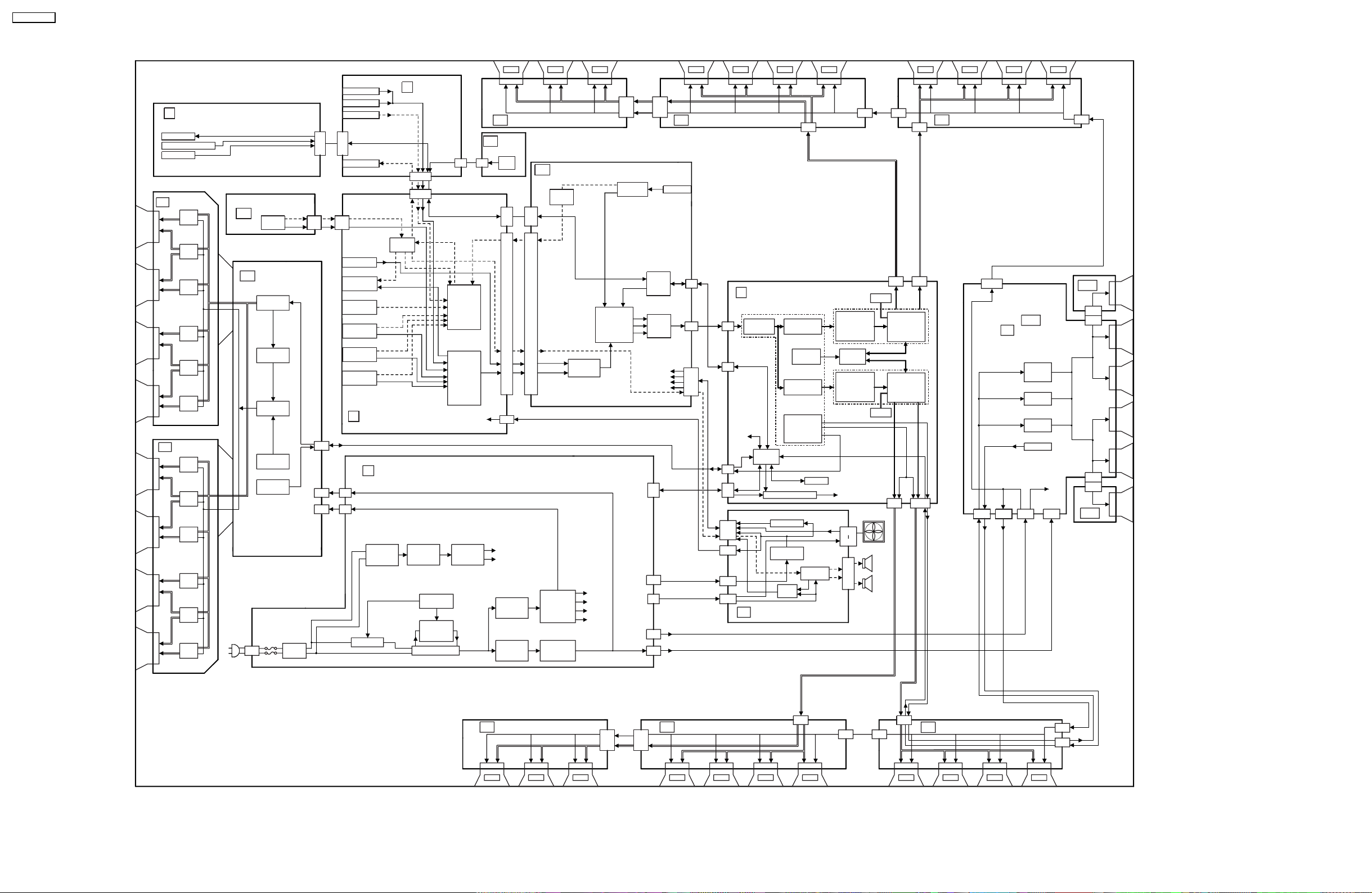
5 Block and Schematic Diagram
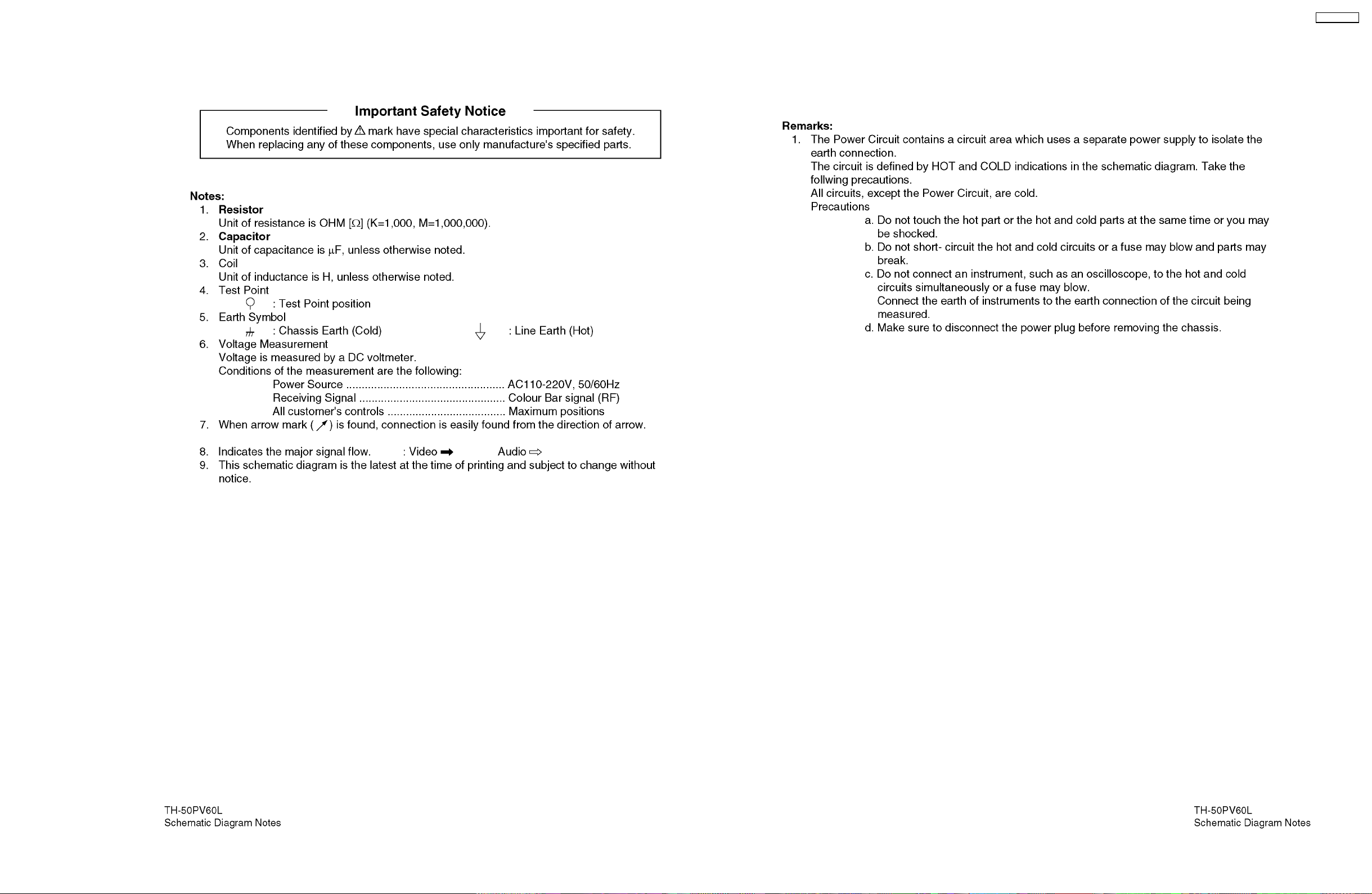
5.1. Schematic Diagram Note
TH-50PV60L
19
TH-50PV60L
5.2. Main Block Diagram
K
REMOTE RECEIVER
LED
POWER LED
REMOTE RECEIVER
AI SENSOR
SCAN OUT
SU
S.R
64
S.R
64
S.R
64
S.R
64
S.R
64
S.R
64
SCAN OUT
SD
S.R
64
S.R
64
S.R
64
S.R
64
S.R
64
S.R
64
TUNER
AC CORD
TU
SC
P9
SIF
MAIN
TV-V1
TUNER
SCAN DRIVE
CONTROL
PULSE
SUSTAIN
PULSE
SCAN
PULSE
VOLTAGE
GENERATOR
SOS6
SOS7
LINE
FILTER
S.R.
AV4 IN
S-VIDEO IN
VIDEO IN
AUDIO IN
G1
K1
HEADPHONE
SIF
H6
TA6
TV-V1
PC IN
MONITOR
OUT
AUDIO
IN
AV1
AV2
AV3
AV TERMINAL,
H
AV SWITCH,MSP
SC20
P
P2
P23
VSUS
15Vd
RECTIFIER
RUSH/MAIN_ON/OFF
RELAY
SC2
SC23
G
AV4 IN
L/R
HP_L/R
G51
H51
MSP
R,G,B
TV_L/R
L/R
L/R
L/R
V,Y, PB ,P R
L/R
V,Y, C
L/R
V,Y, PB ,P R
POWER SUPPLY
PROTECTION(SOS)
STANDBY
VOLTAGE
CONTROL
RELAY,PFC
CONTROL
POWER
FACTOR
CORRECTOR
RECTIFIER
L/R
RECTIFIER
PFC_ON/OFF
G3
AUDIO
INPUT
SELECT
VIDEO
INPUT
SELECT
DC POWER
STANDBY
VOLTAGE
C1
DATA DRIVER(RIGHT)
GK
KEY
SCAN
KEY
GK3
SCAN
H2
H1
H40
+5Vc
STB5V
PROCESS
VOLTAGE
CONTROL
SUSTAIN
VOLTAGE
CONTROL
S.R.
DG
DIGITAL SIGNAL PROCESSOR
AUDIO
DAC
DG2
HDMI
L/R
DG1
MAIN_L/R
PC RGB
Y,P b, Pr
PROCESS
VOLTAGE
RECTIFIER
SUSTAIN
VOLTAGE
RECTIFIER
10bit AD
(ADV7499)
YG/UB
VDA
15Vc
15Vd
F_STB_14V
S.R.
VDA
PROCESSOR
(GC5)
RGB
C10
HDMI I/F
RECEIVER
OSD
STBY5V_M
PS_SOS
F_STB_14V
VSUS
+5V
+15V
+15V
15V
Vda
R
G
B
SOUND SOS
C20
MAIN
MCU
LVDS
TRANSMITTER
FAN SOS
DC POWER
PA SOS
P25
P10
P5
P12
P11
S.R.
DATA DRIVER(CENTER)C2
HDMI IN
DG3
DG5
DG20
D20
D25
PA2 0
PA4 0
PA1 0
S.R.
D
D5
D3
IIC
SOS6/
SOS7
PA5
PA
S.R.
S.R.
C21
FORMAT CONVERTER
PLASMA AI PROCESSOR
LVDS
RECEIVER
MICOM
PICTURE
OUTPUT
FLASH
CONTROL
PICTURE
OUTPUT
FPGA
CONTROL
DISCHARGE
CONTROL
SOS8
SCAN CONTROL
IIC
P_ON/OFF
DC/DC CONVERTER
POWER SOS
DC/DC
CONVERTER
SOUND
SOS
EEPROM
SPEAKER
AMP
FAN SOS
+15V
DC-DC CONVERTER
VDA
C22
SDRAM
FORMAT
CONVERTER
RGB
PROCESSOR
FLASH
MEMORY
FORMAT
CONVERTER
RGB
PROCESSOR PROCESSOR
PA3 1
PA3 4
SDRAM
FAN
SPEAKER
L
PA2
SPEAKER
R
SUSTAIN CONTROL
DATA DRIVE
P3.3V
P2.5V
P1.2V
L
R
S.R. S.R.
C32
C31
D31 D32
VIDEO
DATA
PLASMA AI
SUB-FIELD
PROCESSOR
PLASMA AI
SUB-FIELD
VIDEO
DATA
D33
D34
S.R.
VDA
C3
DATA DRIVER(RIGHT)
SS44
VDA
SS43
S.R.
SS2
SS
SUSTAIN DRIVE
ADDRESS
VOLTAGE
(VE)
SUSTAIN
PULSE
ERASE
PULSE
SS_SOS8
VDA
SS44
SS12
VSUS
SS11
VDA
C33
SS2
SS23
SS21
SS20
+15V
SS22
SS3
TH-50PV60L
Main Block Diagram
DATA DRIVER(LEFT)
C6
S.R. S.R.
S.R.
VDA
C60
C5
DATA DRIVER(CENTER)
C50
S.R.
20
C51
C52
VDA
S.R.
C41
C42
S.R.S.R. S.R.S.R.
DATA DRIVER(RIGHT)
C4
S.R.
S.R.
VDA
VDA
C44
C43
TH-50PV60L
Main Block Diagram
 Loading...