

Page 1
ORDER NO.MTNC090428CE
B34 Canada: B07
54 inch Class 1080p Plasma HDTV
Model No. TC-P54G10
GPF12DU Chassis
© Panasonic Corporation 2009.
Unauthorized copying and distribution is a violation
of law.
Page 2

TABLE OF CONTENTS
PAGE PAGE
1 Safety Precautions -----------------------------------------------3
1.1. General Guidelines ----------------------------------------3
2 Warning --------------------------------------------------------------4
2.1. Prevention of Electrostatic Discharge (ESD)
to Electrostatically Sensitive (ES) Devices ----------4
2.2. About lead free solder (PbF) ----------------------------5
3 Service Navigation------------------------------------------------6
3.1. Service Hint--------------------------------------------------6
3.2. Applicable signals------------------------------------------7
4 Specifications------------------------------------------------------8
5 Service Mode-------------------------------------------------------9
5.1. How to enter into Service Mode------------------------9
5.2. Service tool mode---------------------------------------- 11
5.3. Hotel mode-------------------------------------------------12
6 Troubleshooting Guide---------------------------------------- 13
6.1. Check of the IIC bus lines------------------------------13
6.2. Power LED Blinking timing chart-------------- -------14
6.3. No Power--------------------------------------------------- 15
6.4. No Picture--------------------------------------------------16
6.5. Local screen failure--------------------------------------17
7 Disassembly and Assembly Instructions---------------18
7.1. Remove the Rear cover --------------------------------18
7.2. Remove the P-Board------------------------------------18
7.3. Remove the Side terminal cover and Rear
terminal cover---------------------------------------------18
7.4. Remove the Tuner unit ---------------------------------18
7.5. Remove the A-Board------------------------------------19
7.6. Remove the Speakers ----------------------------------19
7.7. Remove the Control button unit ---------------------- 19
7.8. Remove the GK-Board ---------------------------------19
7.9. Remove the SU-Board----------------------------------20
7.10. Remove the SD-Board----------------------------------20
7.11. Remove the SC-Board----------------------------------20
7.12. Remove the SS2-Board --------------------------------21
7.13. Remove the SS-Board---------------------------------- 21
7.14. Remove the Hanger metals and the Stand
brackets-----------------------------------------------------21
7.15. Remove the C1-Board ----------------------------------22
7.16. Remove the C2-Board ----------------------------------22
7.17. Remove the C3-Board ----------------------------------22
7.18. Remove the Plasma panel section from the
Cabinet assy (glass)-------------------------------------22
7.19. Remove the S-Board------------------------------------23
7.20. Remove the K-Board------------------------------------23
7.21. Replace the plasma panel -----------------------------24
8 Measurements and Adjustments --------------------------25
8.1. Adjustment Procedure ----------------------------------25
8.2. Adjustment-------------------------------------------------28
9 Block Diagram ---------------------------------------------------31
9.1. Main Block Diagram-------------------------------------31
9.2. Block (1/4) Diagram -------------------------------------32
9.3. Block (2/4) Diagram -------------------------------------33
9.4. Block (3/4) Diagram -------------------------------------34
9.5. Block (4/4) Diagram -------------------------------------35
10 Wiring Connection Diagram---------------------------------37
10.1. Caution statement.---------------------------------------37
10.2. Wiring (1)---------------------------------------------------37
10.3. Wiring (2)---------------------------------------------------38
10.4. Wiring (3) - ------------------------------------------------- 39
10.5. Wiring (4) - ------------------------------------------------- 40
10.6. Wiring (5) - ------------------------------------------------- 41
11 Schematic Diagram -------------------------------------------- 43
11.1. Schematic Diagram Note ------------------------------ 43
11.2. P(P-1)-Board (1/2) Schematic Diagram------------ 44
11.3. P(P-1)-Board (2/2) Schematic Diagram------------ 45
11.4. P(P-2)-Board Schematic Diagram------------------- 46
11.5. GK, K and S-Board Schematic Diagram----------- 47
11.6. A-Board (1/22) Schematic Diagram----------------- 48
11.7. A-Board (2/22) Schematic Diagram----------------- 49
11.8. A-Board (3/22) Schematic Diagram----------------- 50
11.9. A-Board (4/22) Schematic Diagram----------------- 51
11.10. A-Board (5/22) Schematic Diagram - ---------------- 52
11.11. A-Board (6/22) Schematic Diagram- ---------------- 53
11.12. A-Board (7/22) Schematic Diagram - ---------------- 54
11.13. A-Board (8/22) Schematic Diagram - ---------------- 55
11.14. A-Board (9/22) Schematic Diagram - ---------------- 56
11.15. A-Board (10/22) Schematic Diagram--------------- 57
11.16. A-Board (11/22) Schematic Diagram --------------- 58
11.17. A-Board (12/22) Schematic Diagram--------------- 59
11.18. A-Board (13/22) Schematic Diag
11.19. A-Board (14/22) Schematic Diagram--------------- 61
11.20. A-Board (15/22) Schematic Diagram--------------- 62
11.21. A-Board (16/22) Schematic Diagram--------------- 63
11.22. A-Board (17/22) Schematic Diagram--------------- 64
11.23. A-Board (18/22) Schematic Diagram--------------- 65
11.24. A-Board (19/22) Schematic Diagram--------------- 66
11.25. A-Board (20/22) Schematic Diagram--------------- 67
11.26. A-Board (21/22) Schematic Diagram--------------- 68
11.27. A-Board (22/22) Schematic Diagram--------------- 69
11.28. C1-Board (1/2) Schematic Diagram ------ -- -------- 70
11.29. C1-Board (2/2) Schematic Diagram ------ -- -------- 71
11.30. C2-Board (1/2) Schematic Diagram ------ -- -------- 72
11.31. C2-Board (2/2) Schematic Diagram ------ -- -------- 73
11.32. C3-Board (1/2) Schematic Diagram ------ -- -------- 74
11.33. C3-Board (2/2) Schematic Diagram ------ -- -------- 75
11.34. SC-Board (1/4) Schematic Diagram ---------------- 76
11.35. SC-Board (2/4) Schematic Diagram ---------------- 77
11.36. SC-Board (3/4) Schematic Diagram ---------------- 78
11.37. SC-Board (4/4) Schematic Diagram ---------------- 79
11.38. SS-Board (1/2) Schematic Diagram ---------------- 80
11.39. SS-Board (2/2) and SS2-Board Schematic
Diagram---------------------------------------------------- 81
12 Printed Circuit Board------------------------------------------ 82
12.1. P(P-1)-Board---------------------------------------------- 82
12.2. P(P-2)-Board---------------------------------------------- 85
12.3. GK, K, S and SS2-Board ------- -- --------------------- 86
12.4. A-Board ---------------------------------------------------- 87
12.5. C1-Board--------------------------------------------------- 90
12.6. C2-Board--------------------------------------------------- 91
12.7. C3-Board--------------------------------------------------- 92
12.8. SC-Board -------------------------------------------------- 93
12.9. SS-Board -------------------------------------------------- 96
13 Exploded View and Replacement Parts List----------- 99
13.1. Exploded View and Mechanical Replacement
Parts List--------------------------------------------------- 99
13.2. Electrical Replacement Parts List ------------------104
ram--------------- 60
2
Page 3
1 Safety Precautions
1.1. General Guidelines
1. When conducting repairs and servicing, do not attempt to modify the equipment, its parts or its materials.
2. When wiring units (with cables, flexible cables or lead wires) are supplied as repair parts and only one wire or some of the
wires have been broken or disconnected, do not attempt to repair or re-wire the units. Replace the entire wiring unit instead.
3. When conducting repairs and servicing, do not twist the Faston connectors but plug t hem straight in or unplug them straight
out.
4. When servicing, observe the original lead dress. If a sh ort circuit is found, replace all parts which have been overheated or
damaged by the short circuit.
5. After servicing, see to it that all the protective devices such as insulation barriers, insulation papers shield s are properly
installed.
6. After servicing, make the following leakage current checks to prevent the customer from being exposed to shock hazards.
1.1.1. Leakage Current Cold Check
1. Unplu g the AC cord and connect a jumper between the
two prongs on the plug.
2. Measure the resistance value, with an ohmmeter,
between the jumpered AC plug and each exposed metallic cabinet part on the equipment such as screwheads,
connectors, control shafts, etc. When the exposed metallic part has a return path to the chassis, the reading
should be between 1Mohm and 5.2Mohm.
When the exposed metal does not have a return path to
the chassis, the reading must be .
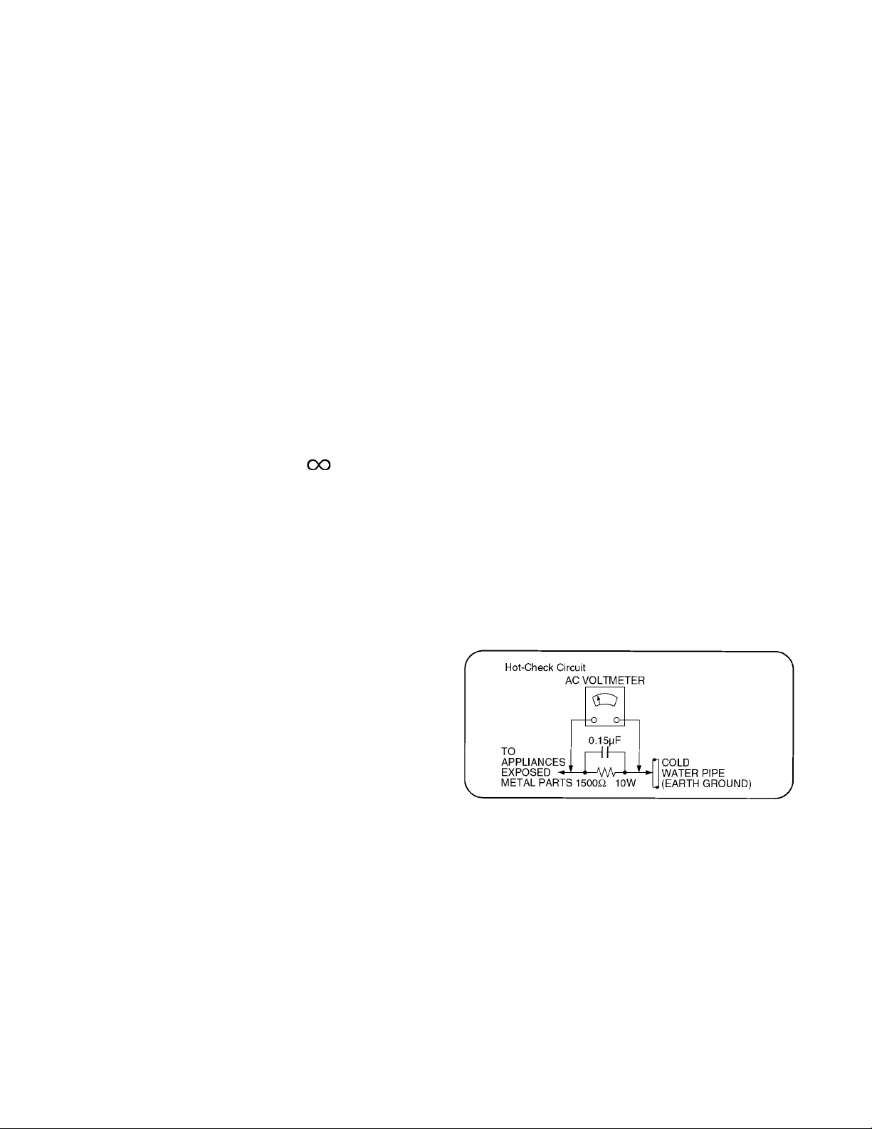
1.1.2. Leakage Current Hot Check (See Figure 1.)
1. Plug the AC cord directly into the AC outlet. Do not use
an isolation transformer for this check.
2. Connect a 1.5kohm, 10 watts resistor, in parallel with a
0.15μF capacitors, between each exposed metallic part
on the set and a good earth ground such as a water pipe,
as shown in Figure 1.
3. Use an AC voltmeter, with 1000 ohms/volt or more sensitivity, to measure the potential across the resistor.
4. Check each exposed metallic part, and measure the voltage at each point.
5. Reverse the AC plug in the AC outlet and repeat each of
the above measurements.
6. The potential at any point should not exceed 0.75 volts
RMS. A leakage current tester (Simpson Model 229 or
equivalent) may be used to make the hot checks, leakage
current must not exceed 1/2 milliamp. In case a measurement is outside of the limits specified, there is a possibility
of a shock hazard, and the equipment should be repaired
and rechecked before it is returned to the customer.
Figure 1
3
Page 4

2 Warning
2.1. Prevention of Electrostatic Discharge (ESD) to Electrostatically Sensitive (ES) Devices
Some semiconductor (solid state) devices can be damaged easily by static electricity. Such components commonly are called Electrostatically Sensitive (ES) Devices. Examples of typical ES devices are integrated circuits and some field-effect transistors and
semiconductor [chip] components. The following techniques should be used to help reduce the incidence of component damage
caused by electrostatic discharge (ESD).
1. Immediately before handling any semiconductor component or semiconductor-equipped assembly, drain off any ESD on your
body by touching a known earth ground. Alternatively, obtain and wear a commercially available discharging ESD wrist strap,
which should be removed for potential shock reasons prior to applying power to the unit under test.
2. After removing an electrica l assembly equ ipped with ES devices, place the assembly on a conductive su rface such as aluminum foil, to prevent electrostatic charge buildup or exposure of the assembly.
3. Use only a grounded-tip soldering iron to solder or unsolder ES devices.
4. Use only an anti-static solder removal device. Some solder removal devices not classified as [anti-static (ESD protected)] can
generate electrical charge sufficient to damage ES devices.
5. Do not use freon-propelled chemicals. These can generate electrical charges sufficient to damage ES devices.
6. Do not remove a replacement ES device from its protective package until immediately before you are ready to install it. (Most
replacement ES devices are packaged with leads electrically shorted together by conductive foam, aluminum foil or comparable conductive material).
7. Immediately before removing the protective material from the leads of a replacement ES device, touch the protective material
to the chassis or circuit assembly into which the device will be installed.
Caution
Be sure no power is applied to the chassis or circuit, and observe all other safety precautions.
8. Minimize bodily motions when handling unpackaged replacement ES devices. (Otherwise ham less motion such as the brushing together of your clothes fabric or the lifting of your foot from a carpeted floor can generate static electricity (ESD) sufficient
to damage an ES device).
4
Page 5
2.2. About lead free solder (PbF)
Note: Lead is listed as (Pb) in the periodic table of elements.
In the information below, Pb will refer to Lead solder, and PbF will refer to Lead Free Solder.
The Lead Free Solder used in our manufacturing process and discussed below is (Sn+Ag+Cu).
That is Tin (Sn), Silver (Ag) and Copper (Cu) although other types are available.
This model uses Pb Free solder in it’s manufacture due to environmental conservation issues. For service and repair work, we’d
suggest the use of Pb free solder as well, although Pb solder may be used.
PCBs manufactured using lead free solder will have the PbF within a leaf Symbol PbF stamped on the back of PCB.
Caution
• Pb free solder has a higher melting point than standard solder. Typically the melting point is 50 ~ 70 °F (30~40 °C) higher. Please
use a high temperature soldering iron and set it to 700 ± 20 °F (37 0 ± 10 °C).
• Pb free solder will tend to splash when heated too high (about 1100 °F or 600 °C).
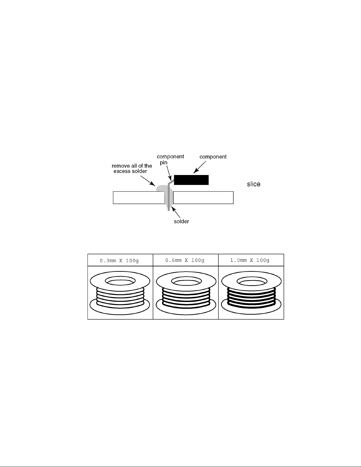
If you must use Pb solder, please completely remove all of the Pb free solder on the pins or solder area before applying Pb solder. If this is not practical, be sure to heat the Pb free solder until it melts, before applying Pb solder.
• After applying PbF solder to double layered boards, please check the component side for excess solder which may flow onto the
opposite side. (see figure below)
Suggested Pb free solder
There are several kinds of Pb free solder available for purchase. This product uses Sn+Ag+Cu (tin, silver, copper) solder. However, Sn+Cu (tin, copper), Sn+Zn+Bi (tin, zinc, bismuth) solder can also be used.
5
Page 6

3 Service Navigation
3.1. Service Hint
Board Name Function Board Name Function
P Power Supply C1 Data Driver (Lower Right)
C2 Data Driver (Lower Center)
A DC-DC Converter, Tuner
Speaker out, AV Terminal, AV Switch
Digital Signal Processor, SYSTEM MPU, HDMI Switch
Seine 3LV
Format Converter, Plasma AI, Sub-Field Processor
K Remote receiver, Power LED, C.A.T.S sensor
SPower Switch
GK Key Switch
C3 Data Driver (Lower Left)
SC Scan Drive
SS Sustain Drive
SS2 Sustain out (Lower)
SU Scan out (Upper)
Non-serviceable.
SU-Board should be exchanged for service.
SD Scan out (Lower)
Non-serviceable.
SD-Board should be exchanged for service.
6
Page 7
3.2. Applicable signals
* Mark: Applicable input signal for Component (Y, PB, PR), HDMI and PC
horizontal frequency (kHz) vertical frequency (Hz) COMPONENT HDMI PC
525 (480) / 60i 15.73 59.94 * *
525 (480) /60p 31.47 59.94 * *
750 (720) /60p 45.00 59.94 * *
1,125 (1,080) /60i 33.75 59.94 * *
1,125 (1,080) /60p 67.43 59.94 *
1,125 (1,080) /60p 67.50 60.00 *
1,125 (1,080) /24p 26.97 23.98 *
1,125 (1,080) /24p 27.00 24.00 *
640 × 400 @70 31.47 70.08 *
640 × 480 @60 31.47 59.94 *
Macintosh13 inch (640 × 480) 35.00 66.67 *
640 × 480 @75 37.50 75.00 *
852 × 480 @60 31.47 59.94 *
800 × 600 @60 37.88 60.32 *
800 × 600 @75 46.88 75.00 *
800 × 600 @85 53.67 85.08 *
Macintosh16 inch (832 × 624) 49.73 74.55 *
1,024 × 768 @60 48.36 60.00 *
1,024 × 768 @70 56.48 70.07 *
1,024 × 768 @75 60.02 75.03 *
1,024 × 768 @85 68.68 85.00 *
Macintosh 21 inch (1,152 ×870) 68.68 75.06 *
1,280 × 1,024 @60 63.98 60.02 *
1,366 × 768 @60 48.36 60.00 *
Note
• Signals other than above may not be displayed properly.
• The above signals are reformatted for optimal viewing on your display.
7
Page 8

4 Specifications
Power Source AC 120 V, 60 Hz
Power Consumption
Maximum 604 W
Standby condition 0.2 W
Plasma Display panel
Drive method AC type
Aspect Ratio 16:9
Visible screen size 54 inch class (54.1 inches measured diagonally)
(W × H × Diagonal) 47.1 inch × 26.5 inch × 54.1 inch (1,198 mm × 673 mm × 1,374 mm)
(No. of pixels) 2,073,600 (1,920 (W) × 1,080 (H))[5,760 × 1,080 dots]
Sound
Audio Output 20 W [ 10 W + 10 W ] ( 10 % THD )
PC signals VGA, SVGA, XGA, WXGA, SXGA
Channel Capability (Digital/Analog) VHF/ UHF: 2 - 69, CATV: 1 - 135
Operating Conditions
Connection Terminals
VIDEO IN 1 VIDEO: RCA PIN Type × 1 1.0 V [p-p] (75 Ω)
VIDEO IN 2 VIDEO: RCA PIN Type × 1 1.0 V [p-p] (75 Ω)
COMPONENT INPUT 1-2 Y: 1.0 V [p-p] (including synchronization)
HDMI 1-3 TYPE A Connector × 3
PC D-SUB 15PIN: R,G,B / 0.7 V [p-p] (75 Ω)
LAN (for VIERA CAST IPTV) RJ45 (10BASE-T/100BASE-TX)
Card slot SD CARD slot × 1
AUDIO OUT AUDIO L-R: RCA PIN Type
DIGIT
AL AUDIO OUT PCM / Dolby Digital, Fiber Optic
FEATURES 3D Y/C FILTER CLOSED CAPTION
Dimensions (W × H × D)
Including pedestal 51.7 inch × 34.8 inch × 15.3 inch (1,313 mm × 882 mm × 387 mm)
TV Set only 51.7 inch × 32.8 inch × 3.8 inch (4.3 inch) (1,313 mm × 832 mm × 96 mm (107 mm))
Mass
Including pedestal 90.4 lb. (41.0 kg)
TV Set only 83.8 lb. (38.0 kg)
Horizontal scanning frequency 31 - 69 kHz
Vertical scanning frequency 59 - 86 Hz
Temperature: 32 °F - 104 °F (0 °C - 40 °C)
Humidity: 20 % - 80 % RH (non-condensing)
S-VIDEO: Mini DIN 4-pin Y: 1.0 V [p-p] (75 Ω) C: 0.286 V [p-p] (75 Ω)
AUDIO L-R: RCA PIN Type × 2 0.5 V [rms]
AUDIO L-R: RCA PIN Type × 2 0.5 V [rms]
PB, PR: ±0.35 V [p-p]
AUDIO L-R: RCA PIN Type × 2 0.5 V [rms]
This TV supports [HDAVI Control 4] function.
HD, VD / 1.0 - 5.0 V [p-p] (high impedance)
V-Chip IPTV (VIERA CAST)
Photo Viewer Movie player
HDAVI Control 4
× 2
0.5 V [rms]
Note
• Design and Specifications are subject to change without notice. Mass and Dimensions shown are approximate.
8
Page 9
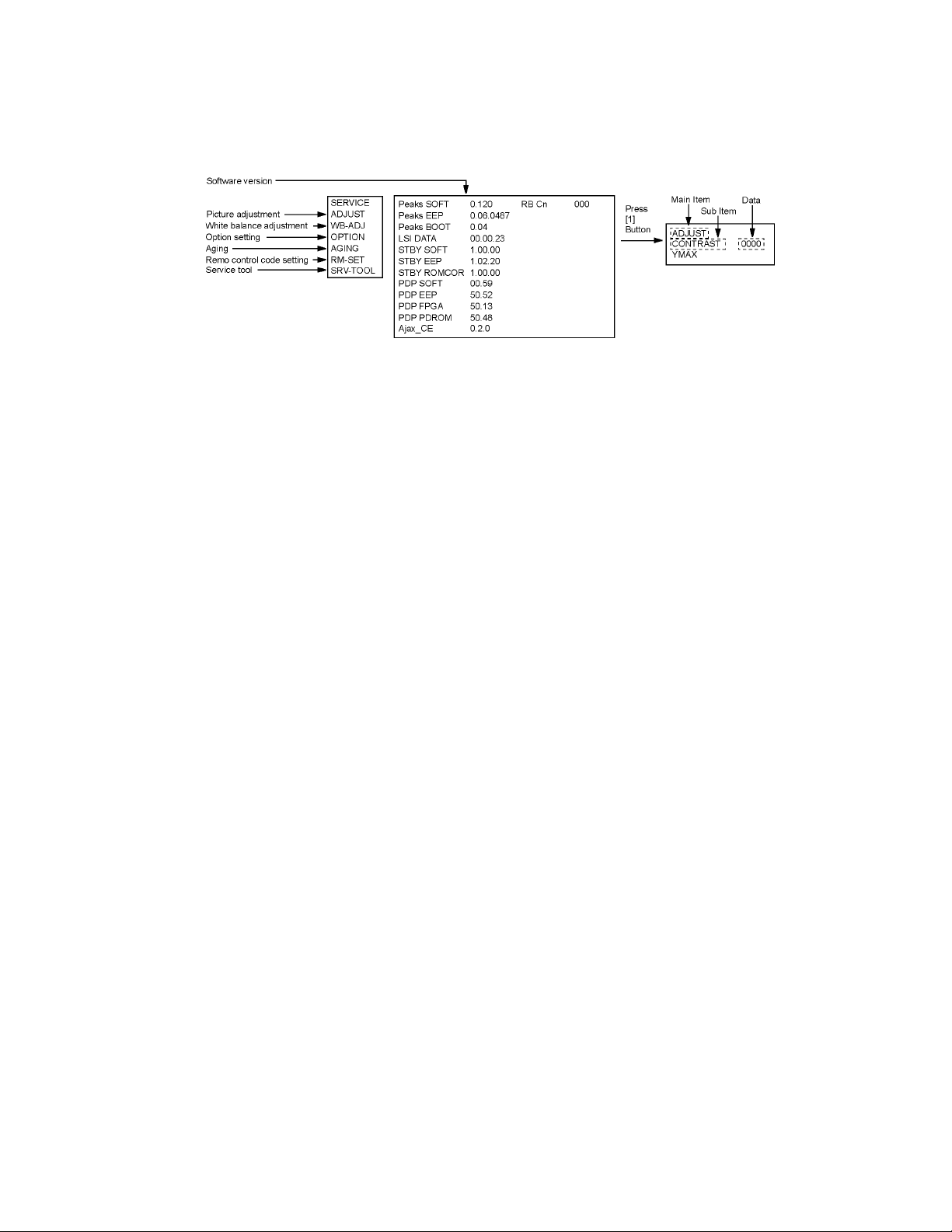
5 Service Mode
5.1. How to enter into Service Mode
While pressing [VOLUME ( - )] button of the main unit, press [INFO] button of the remote control three times within 2 seconds.
5.1.1. Key command
[1] button...Main items Selection in forward direction
[2] button...Main items Selection in reverse direction
[3] button...Sub items Selection in forward direction
[4] button...Sub items Selection in reverse direction
[VOL] button...Value of sub items change in forward direction ( + ), in reverse direction ( - )
9
Page 10
5.1.2. Contents of adjustment mode
• Value is shown as a hexadecimal number.
• Preset value differs depending on models.
• After entering the adjustment mode, take note of the value in each item before starting adjustment.
Main item Sub item Sample Data Remark
ADJUST CONTRAST 46
COLOR 00
TINT 00
SUB-BRT 000
WB-ADJ R-CUT 80
G-CUT 80
B-CUT 80
R-DRV FC
G-DRV FF
B-DRV E8
ALL-CUT 80
ALL-DRV FC
OPTION BOOT ROM Factory Preset
STBY-SET - EMERGENCY ON
CLK MODE 00
CLOCK 000
AGING RGBW
VERTICAL LINE
COUNT
ALL WHITE
ALL RED
ALL GREEN
ALL BLUE
ON/OFF
RAMP WHITE
RAMP RED
RAMP GREEN
RAMP BLUE
1% WINDOW
COLOR BAR
A-ZONE B-ZONE/4 TRIO
SCROLL
WHITE FLAME
LOW SETUP RED
LOW SETUP GREEN
LOW SETUP BLUE
RM-SET CODE A Fixed
SRV-TOOL - See next
5.1.3. How to exit
Switch off the power with the [POWER] button on the main unit or the [POWER] button on the remote control.
10
Page 11
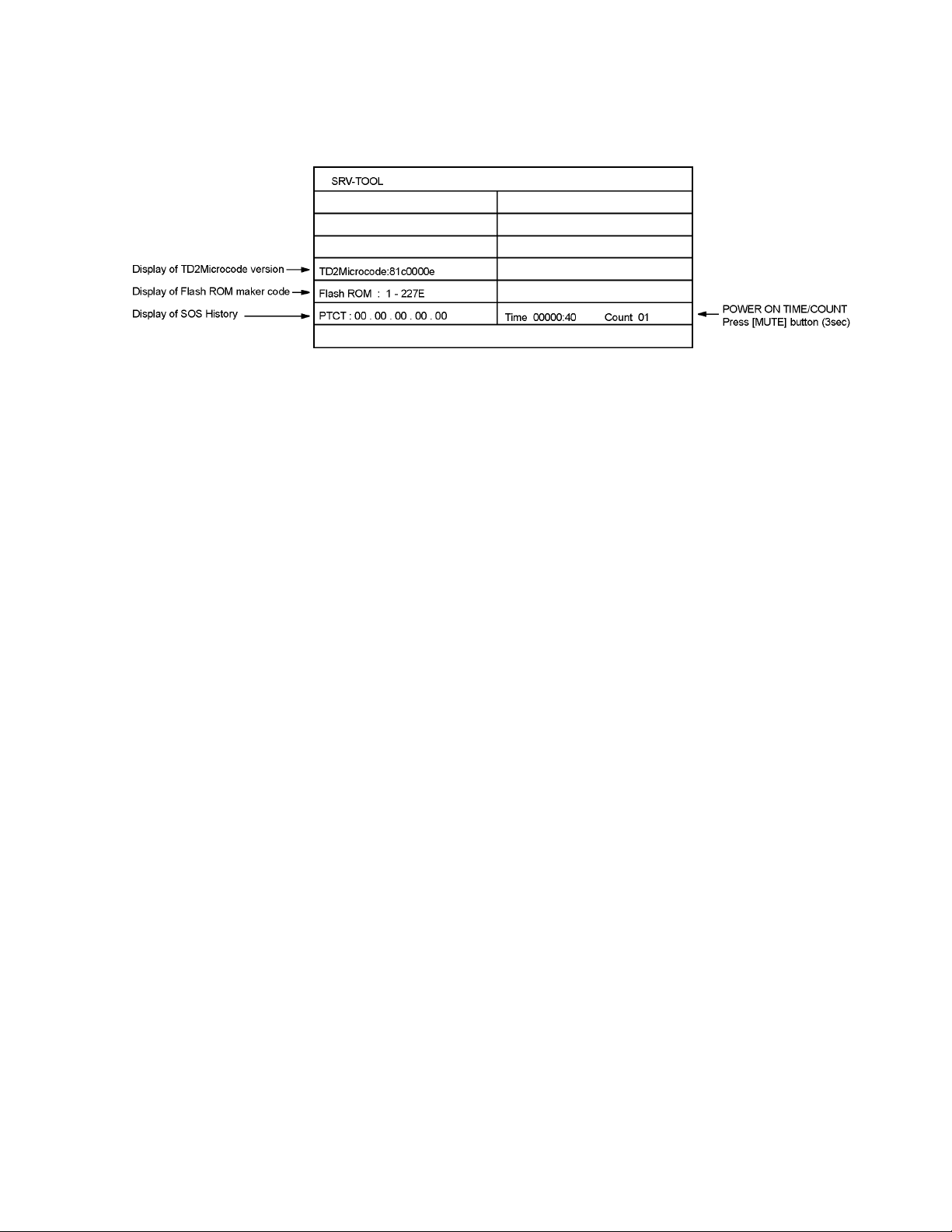
5.2. Service tool mode
5.2.1. How to access
1. Select [SRV-TOOL] in Service Mode.
2. Press [OK] button on the remote control.
5.2.2. Display of SOS History
SOS History (Number of LED blinking) indication.
From left side; Last SOS, before Last, three occurrence before, 2nd occurrence after shipment, 1st occurrence after shipment.
This indication except 2nd and 1st occurrence after shipment will be cleared by [Self-check indication and forced to factory shipment setting].
5.2.3. POWER ON TIME/COUNT
Note : To display TIME/COUNT menu, highlight position, then press MUTE for (3sec).
Time : Cumulative power on time, indicated hour : minute by decimal
Count : Number of ON times by decimal
Note : This indication will not be cleared by either of the self-checks or any other command.
5.2.4. Exit
1. Disconnect the AC cord from wall outlet.
11
Page 12
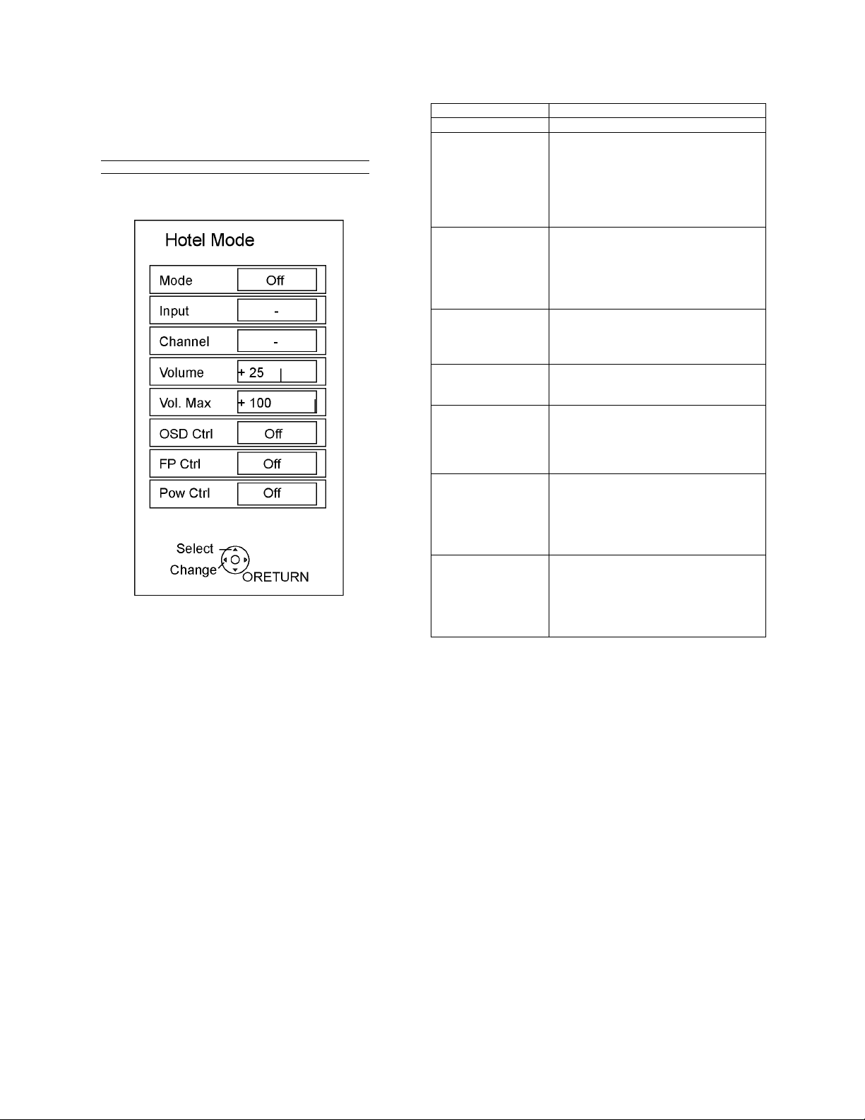
5.3. Hotel mode
1. Purpose
Restrict a function for hotels.
2. Access command to the Hotel mode setup menu
In order to display the Hotel mode setup menu, please
enter the following command (within 2 second).
[TV] : Vol. [Down] + [REMOTE] : INPUT (3 times)
Then, the Hotel mode setup menu is displayed.
3. To exit the Hotel mode setup menu
Disconnect AC power cord from wall outlet.
4. Explain the Hotel mode setup menu
item Function
Mode Select hotel mode ON/OFF
Input Select input signal modes.
Set the input, when each time power is
switched on.
Selection:
-/RF/COMP1/COMP2/HDMI1/HDMI2/
HDMI3/VIDEO1/VIDEO2/PC
• Off: give priority to a last memory.
Channel Select channel when input signal is RF.
Set the channel, each time power is switched
on.
Selection:
Any channel number or [-].
[-] means the channel when turns off.
Volume Adjust the volume when each time p ower is
switched on.
Range:
0 to 100
Vol. Max Adjust maximum volume.
Range:
0 to 100
OSD Ctrl Restrict the OSD.
Selection:
OFF/PATTERN1
• OFF: No restriction
• PATTERN1: restriction
FP Ctrl Select front key conditions.
Selection:
Off/Pattern1/All
• Off: altogether valid.
• Pattern: only input key is valid.
• All: altogether invalid.
Pow Ctrl Select POWER-ON/OFF con dition when AC
power cord is disconnected and then connected.
OFF: The same condition when AC power
cord is disconnected.
ON: Forced power ON condition.
12
Page 13

6 Troubleshooting Guide
Use the self-check function to test the unit.
1. Checking the IIC bus lines
2. Power LED Blinking timing
6.1. Check of the IIC bus lines
6.1.1. How to access
Self-check indication only:
Produce TV reception screen, and while pressing [VOLUME ( - )] button on the main unit, press [OK] button on the remote control
for more than 3 seconds.
Self-check indication and forced to factory shipment setting:
Produce TV reception screen, and while pressing [VOLUME ( - )] button on the main unit, press [MENU] button on the remote control for more than 3 seconds.
6.1.2. Exit
Disconnect the AC cord from wall outlet.
6.1.3. Screen display
6.1.4. Check Point
Confirm the following parts if NG was displayed.
13
Page 14
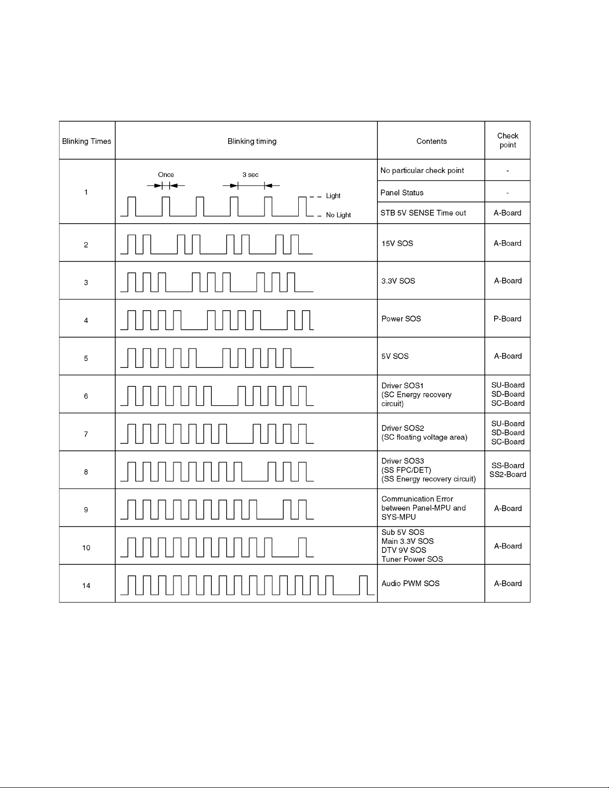
6.2. Power LED Blinking timing chart
1. Subject
Information of LED Flashing timing chart.
2. Contents
When an abnormality has occurred the unit, the protection circuit operates and reset to the stand by mode. At this time, the
defective block can be identified by the number of blinks of the Power LED on the front panel of the unit.
14
Page 15
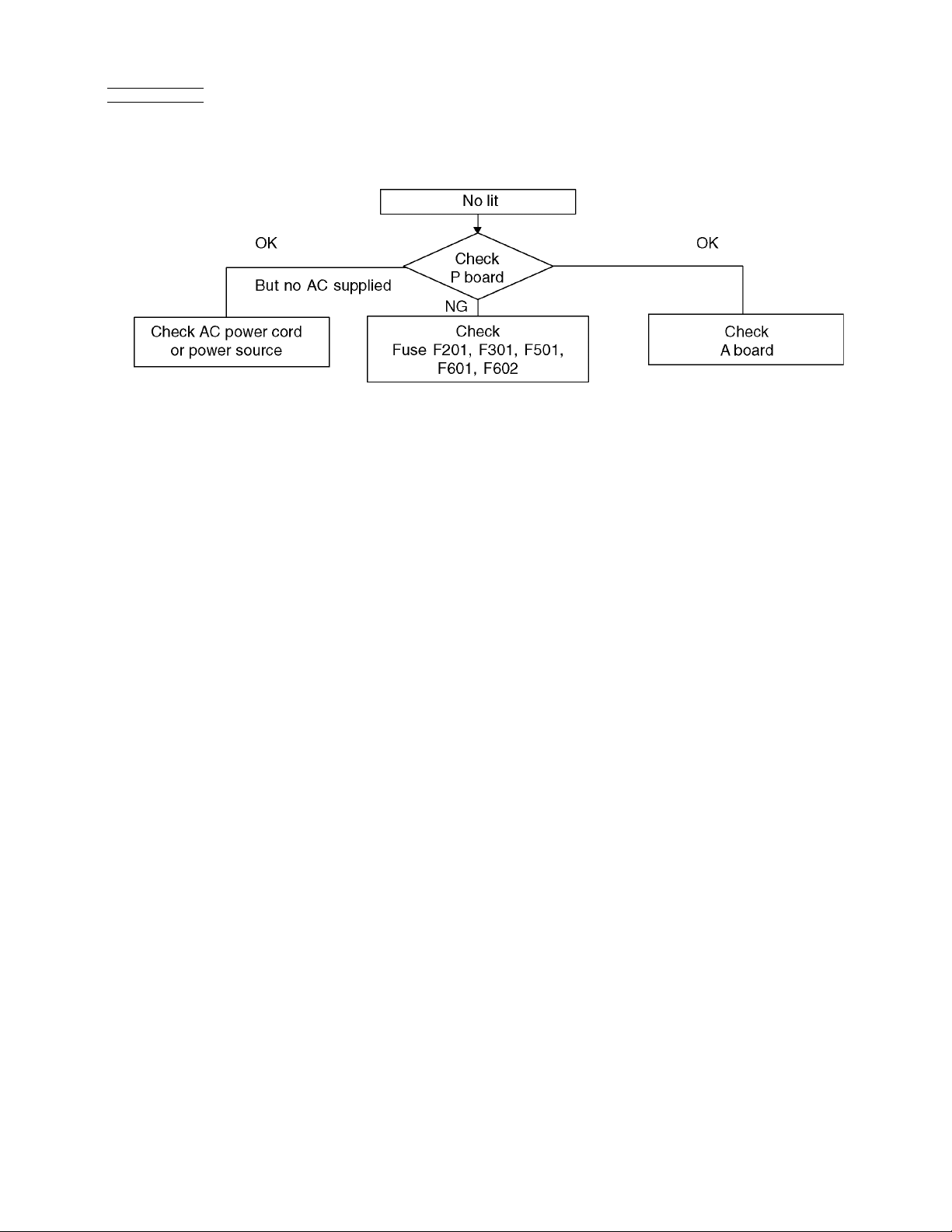
6.3. No Power
First check point
There are following 2 states of No Power indication by power LED.
1. No lit
2. Red is lit then turns red blinking a few seconds later. (See 6.2.)
15
Page 16
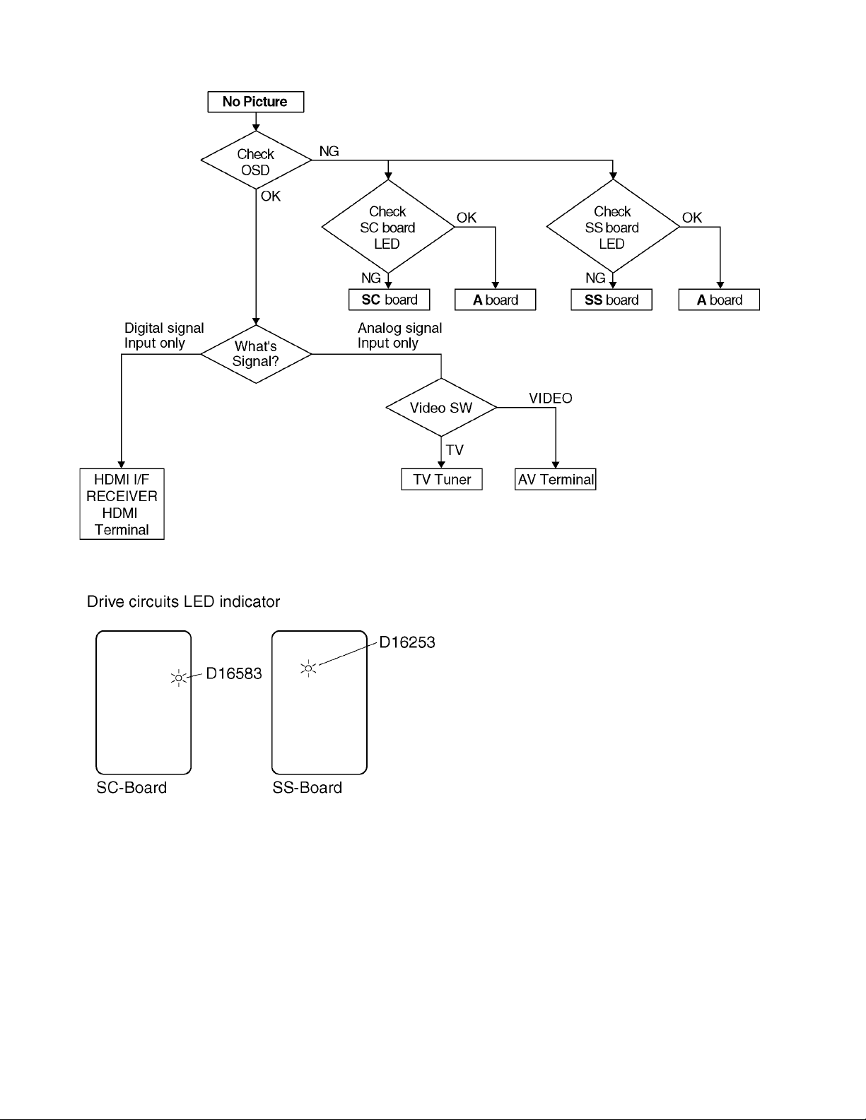
6.4. No Picture
16
Page 17
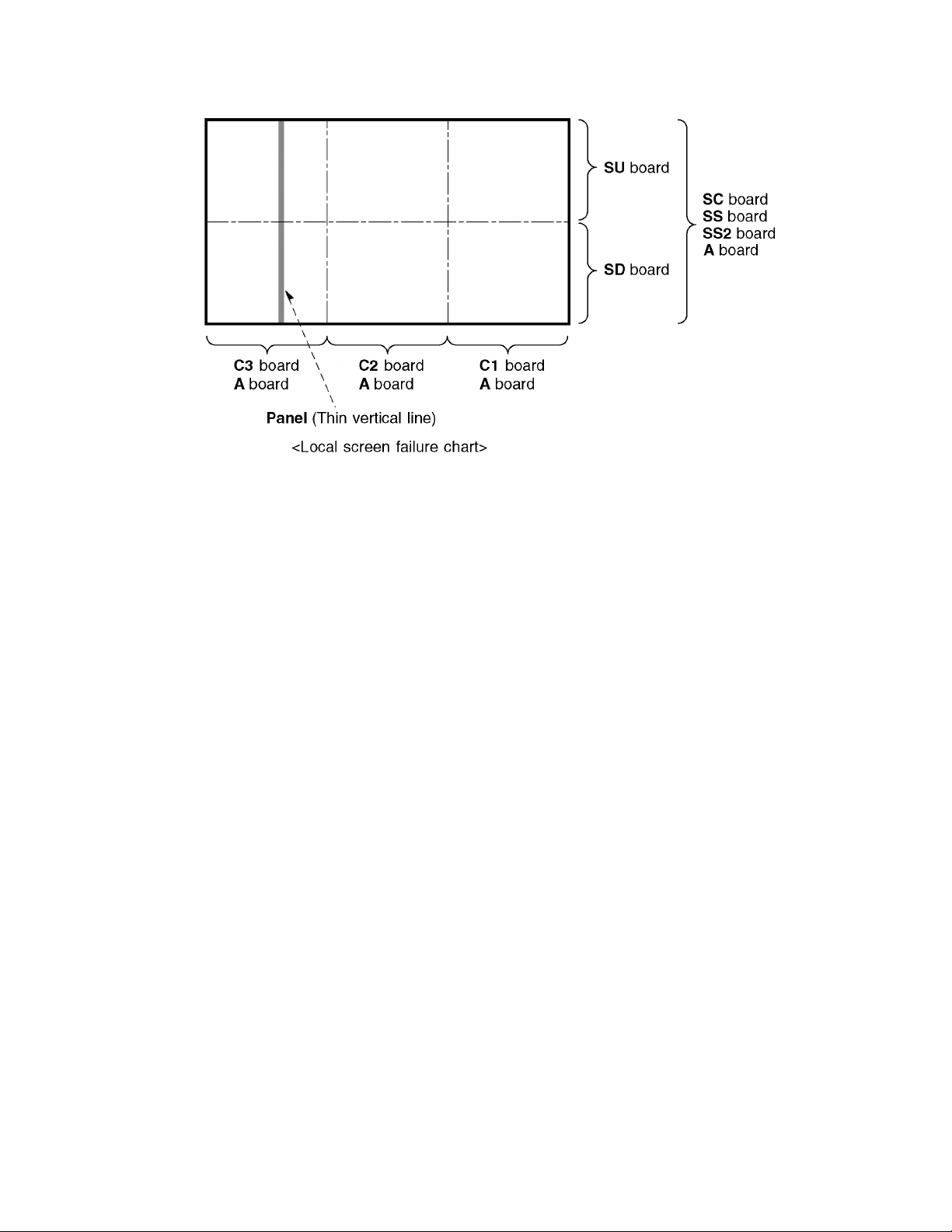
6.5. Local screen failure
Plasma display may have local area failure on the screen. Fig-1 is the possible defect P.C.B. for each local area.
Fig-1
17
Page 18

7 Disassembly and Assembly Instructions
7.1. Remove the Rear cover
1. See Service Hint (Section 3)
7.2. Remove the P-Board
Caution:
To remove P.C.B. wait 1 minute after power was off for discharge from electrolysis capacitors.
1. Unlock the cable clampers to free the cable
2. Disconnect the connectors (P51-P52, P53-P54, P55-P56
and P57-P58).
3. Disconnect the connectors (P2, P6, P7, P9, P11, P25 and
P35).
4. Remove the screws (×9 ) and remove the
P(P-1)-Board.
5. Remove the screws (×6 ) and remove the
P(P-2)-Board.
3. Remove the Adjustment cover.
4. Remove the screws (×4 , ×3 , ×1 ).
5. Remove the Rear terminal cover.
7.4. Remove the Tuner unit
1. Unlock the cable clampers to free the cable.
2. Disconnect the connectors (A1, A6 A11, A12, A25 and
A30).
3. Disconnect the flexible cables (A31, A32 and A33).
4. Remove the screws (×2 ) and remove the Tuner unit.
7.3. Remove the Side terminal cover and Rear terminal cover
1. Remove the claw (×1 ).
2. Remove the Side terminal cover.
18
Page 19
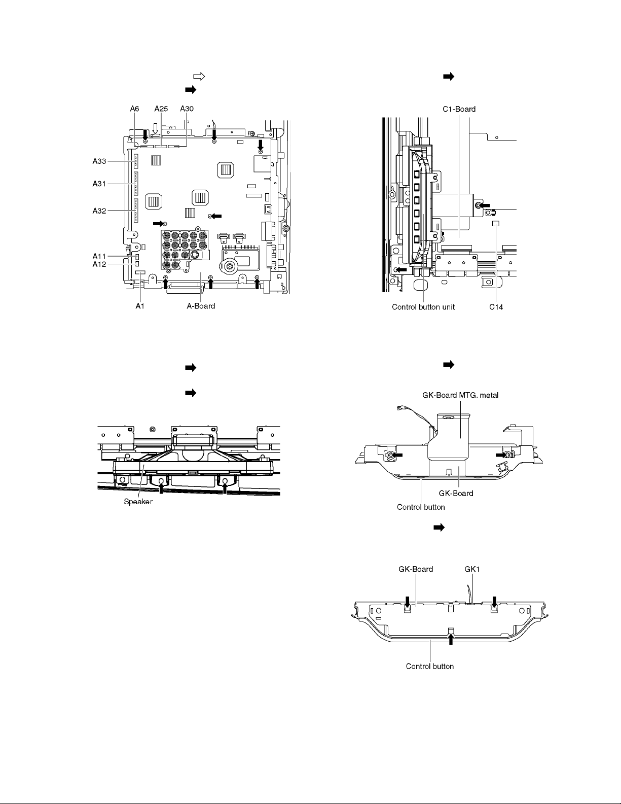
7.5. Remove the A-Board
1. Remove the Tuner unit. (See section 7.4.)
2. Remove the clampers (×2 ).
3. Remove the screws (×8 ) and remove the A-Board.
7.7. Remove the Control button unit
1. Disconnect the connector (C14).
2. Remove the screws (×2 ).
3. Remove the Control button unit.
7.6. Remove the Speakers
1. Unlock the cable clampers to free the cable.
2. Disconnect the relay connector.
3. Remove the screws (×2 ) and remove the Speaker R.
4. Disconnect the connector (A12). (See section 7.4.)
5. Remove the screws (×2 ) and remove the Speaker L.
7.8. Remove the GK-Board
1. Remove the Control button unit. (See section 7.7.)
2. Remove the screws (×2 ).
3. Remove the GK-Board MTG. metal.
4. Remove the claw (×3 ).
5. Disconnect the connector (GK1).
6. Remove the GK-Board from Control button.
19
Page 20
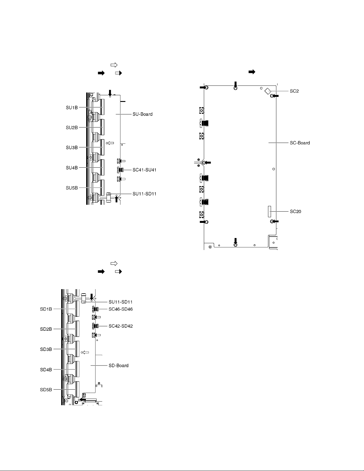
7.9. Remove the SU-Board
1. Re move the flexible cables (SU1B, SU2B, SU3B, SU4B
and SU5B) connected to the SU-Board.
2. Remove the flexible cable (SU11-SD11) and the bridge
connector (SC41-SU41).
3. Remove the molding prop (×1 ).
4. Remove the screws (×2 , ×2 ) and remove the SU-
Board.
7.11. Remove the SC-Board
1. Remove the SU-Board and SD-Board. (See section 7.9.
and 7.10.)
2. Unlock the cable clampers to free the cable.
3. Disconnect the connector (SC2).
4. Disconnect the flexible cable (SC20).
5. Remove the screws (×7 ) and remove the SC-Board.
7.10. Remove the SD-Board
1. Remove the Control button unit. (See section 7.7.)
2. Re move the flexible cables (SD1B, SD2B, SD3B, SD4B
and SD5B) connected to the SD-Board.
3. Remove the flexible cable (SU11-SD11) and the bridge
connectors (SC42-SD42 and SC46-SD46).
4. Remove the molding prop (×1 ).
5. Remove the screws (×2 , ×2 ) and remove the SD-
Board.
20
Page 21
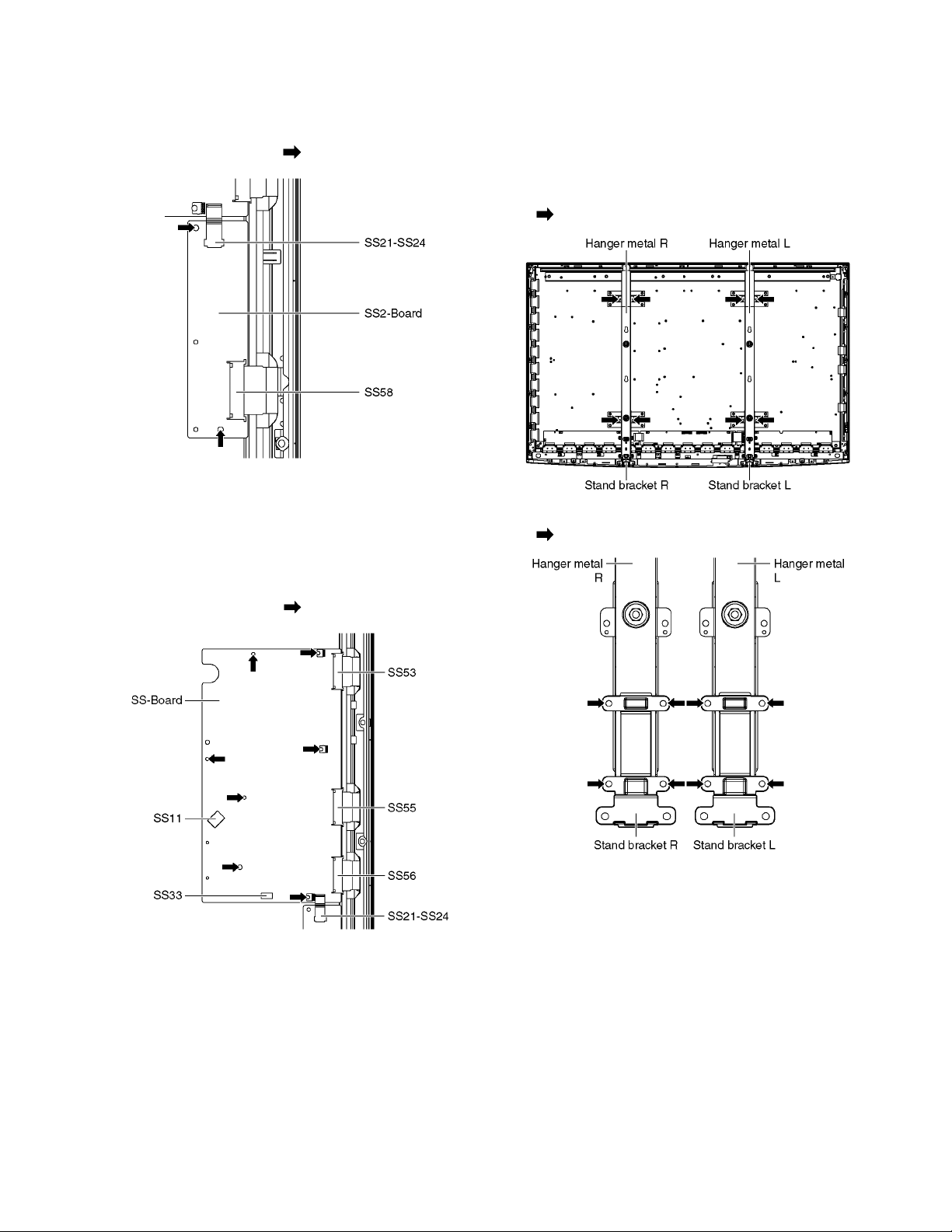
7.12. Remove the SS2-Board
1. Remove the Tuner unit. (See section 7.4.)
2. Disconnect the bridge connector (SS21-SS24) and disconnect the flexible cable (SS58).
3. Remove the screws (×2 ) and remove the SS2-Board.
7.13. Remove the SS-Board
1. Remove the Tuner unit. (See section 7.4.)
2. Unlock the cable clampers to free the cable.
3. Disconnect the connectors (SS11 and SS33).
4. Disconnect the flexible cables (SS53, SS55 and SS56).
5. Disconnect the bridge connector (SS21-SS24).
6. Remove the screws (×7 ) and remove the SS-Board.
7.14. Remove the Hanger metals and the Stand brackets
1. Remove the Plasma panel section from the servicing
stand and lay on a flat surface such as a table (covered
by a soft cloth) with the Plasma panel surface facing
downward.
2. Remove the Hanger metals (L, R) fastening screws (×4
each) and remove the Hanger metals (L, R).
3. Remove the Stand brackets (L, R) fastening screws (×4
each) and the Stand brackets (L, R).
21
Page 22
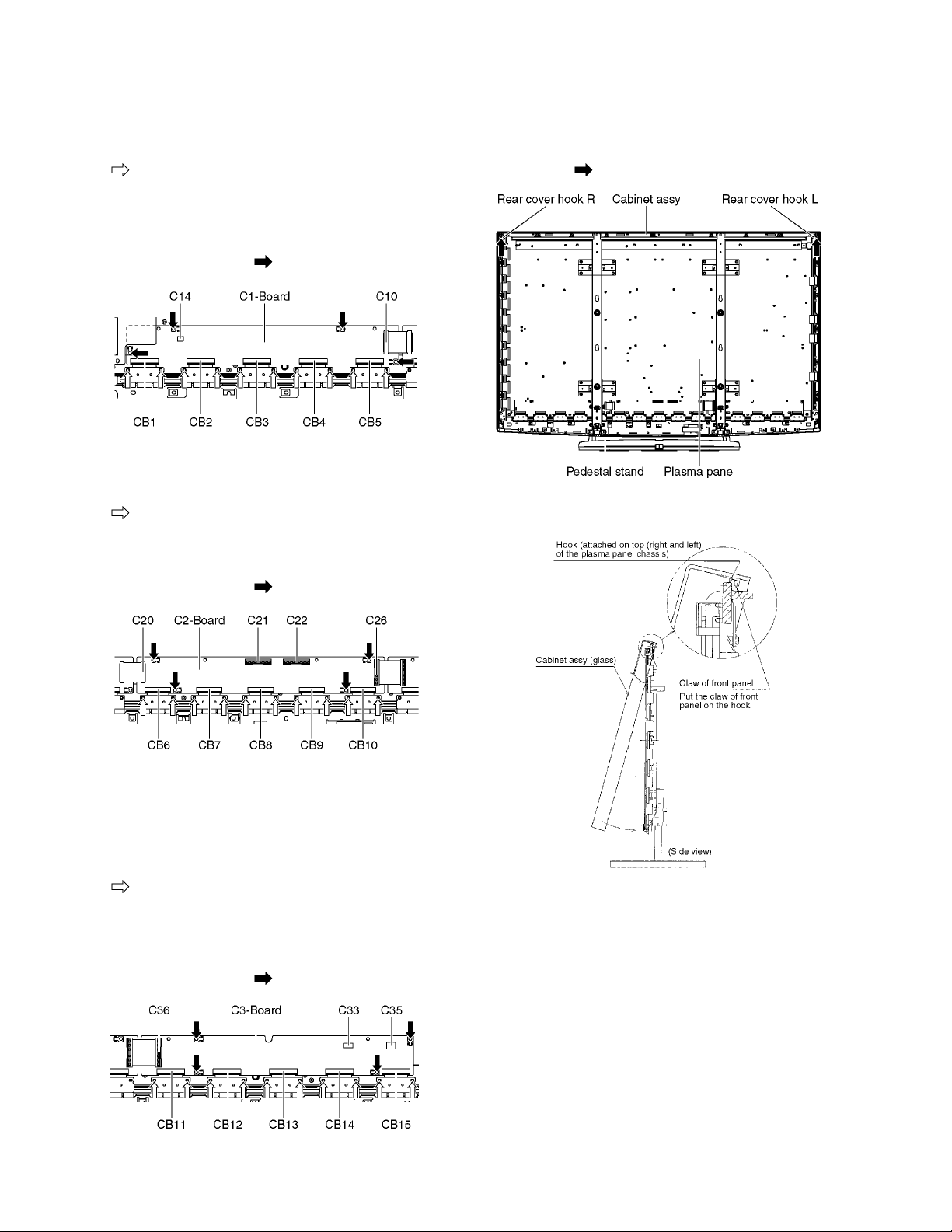
7.15. Remove the C1-Board
1. Remove the Control button unit. (See section 7.7.)
2. Re move the Hanger metal R and the Stand bracket R.
(See section 7.14.)
3. Remove the flexible cables holder fastening screws (×10
).
4. Discon nect the flexible cab les (CB1, CB2, CB3, CB4 and
CB5).
5. Disconnect the flexible cable (C10).
6. Disconnect the connector (C14).
7. Remove the screws (×4 ) and remove the C1-Board.
7.16. Remove the C2-Board
1. Remove the flexible cables holder fastening screws (×10
).
2. Discon nect the flexible cab les (CB6, CB7, CB8, CB9 and
CB10).
3. Disconnect the flexible cables (C20, C21, C22 and C26).
4. Remove the screws (×4 ) and remove the C2-Board.
7.18. Remove the Plasma panel section from the Cabinet assy
(glass)
1. Remove the cabinet assy and the plasma panel fastening
screws (×2 ).
2. For leaving the plasma panel from the front frame, pull the
bottom of the cabinet assy forward, lift, and remove.
7.17. Remove the C3-Board
1. Remove the Tuner unit. (See section 7.4.)
2. Remove the Hanger metal L and the Stand bracket L.
(See section 7.14.)
3. Remove the flexible cables holder fastening screws (×10
).
4. Disconnect the flexible cables (CB11, CB12, CB13, CB14
and CB15).
5. Disconnect the flexible cable (C36).
6. Disconnect the connectors (C33 and C35).
7. Remove the screws (×5 ) and remove the C3-Board.
22
Page 23
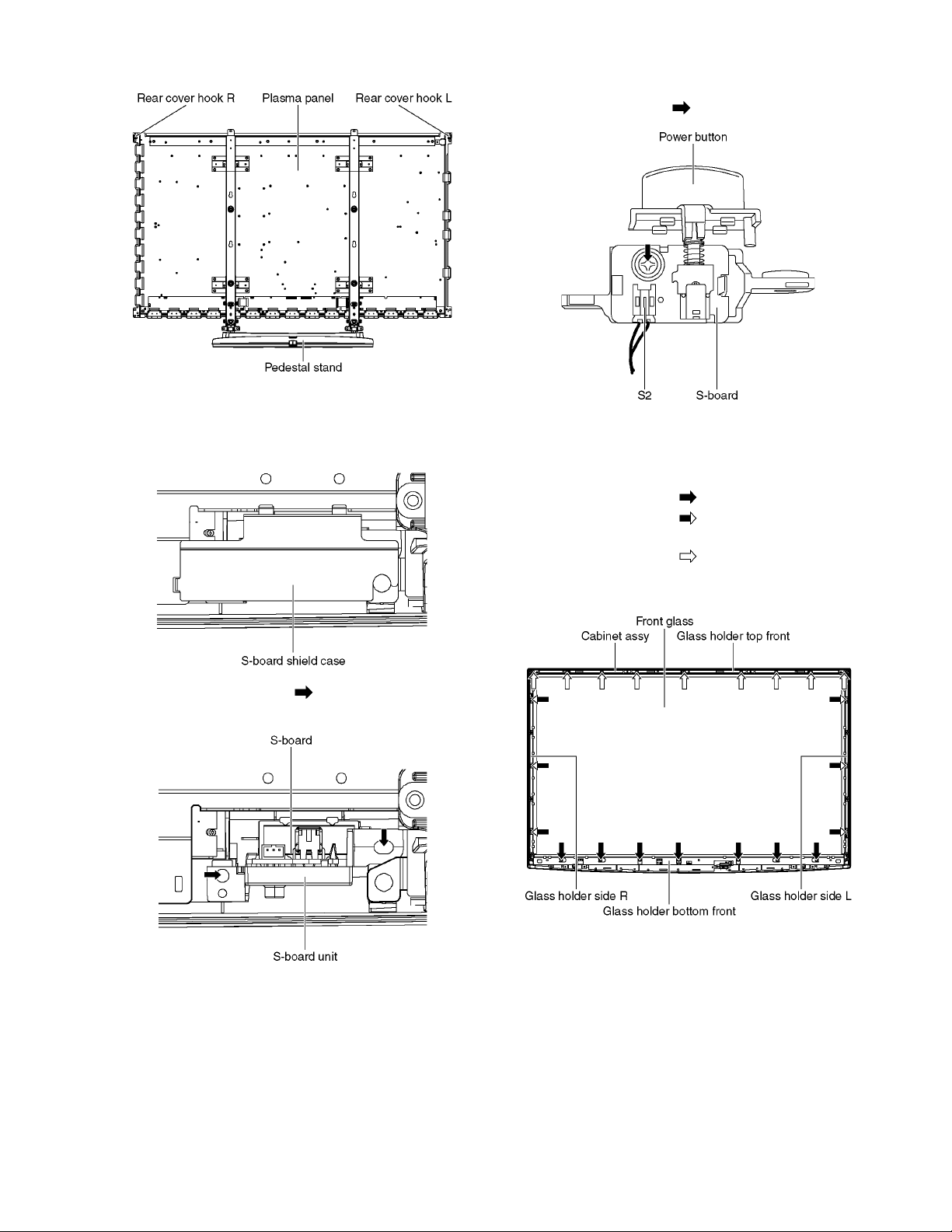
3. Remove the Rear cover hooks (L, R).
7.19. Remove the S-Board
1. Remove the Cabinet assy. (See section 7.18.)
2. Remove the S-Board shield case.
4. Disconnect the connector (S2).
5. Remove the Power button.
6. Remove the screw (×1 ) and remove the S-Board.
7.20. Remove the K-Board
1. Remove the Cabinet assy. (See section 7.18.)
2. Remove the S-Board. (See section 7.19.)
3. Remove the screws (×7 ).
4. Remove the screws (×6 ).
5. Remove the Glass holder side (L, R).
6. Remove the screws (×9 ).
7. Remove the Glass holder top front.
8. Remove the Glass holder bottom front.
3. Remove the screws (×2 ) and remove the S-Board
unit.
23
Page 24
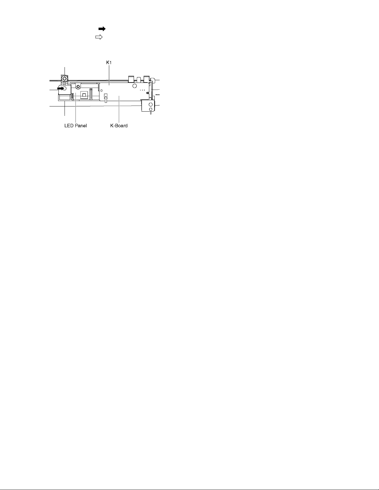
9. Remove the screw (×1 ).
10. Remove the claw (×1 ).
11. Disconnect the connector (K1) and remove the K-Board
from LED Panel.
7.21. Replace the plasma panel
Caution:
A new plasma panel itself without Hanger metals is
fragile.
To avoid the damage to new plasma panel, carry a new
plasma panel taking hold of the Hanger metals after
assembling the Hanger metals and the Stand brackets.
1. Place a carton box packed a new plasma panel on the flat
surface of the work bench.
2. Open a box and without taking a new plasma panel;
Attach the C1-Board, C2-Board and the C3-Board, connect the flexible cables from the plasma panel to the C1Board, C2-Board and the C3-Board, and fit the flexible
cable holders.
3. Attach the Hanger metals and the Stand brackets to the
new plasma panel.
4. Place the plasma panel on the servicing stand taking hold
of the Hanger metals.
5. Attach the cabinet assy and each P.C.Board and so on, to
the new plasma panel.
*When fitting the cabinet assy, be careful not to allow any
debris, dust or handling residue to remain between the
front glass and plasma panel.
24
Page 25
8 Measurements and Adjustments
8.1. Adjustment Procedure
8.1.1. Driver Set-up
8.1.1.1. Item / Preparation
1. Input a white signal to plasma video input.
2. Set the picture controls as follows.
Picture menu: Vivid
Normal: Set
Aspect: Full
Caution
1. First perform Vsus adjustment.
2. The Vscn voltages are measured from the Vad (Vad_base), but may be measured from the GND (GND_base) in an
unavoidable case.
8.1.1.2. Adjustments
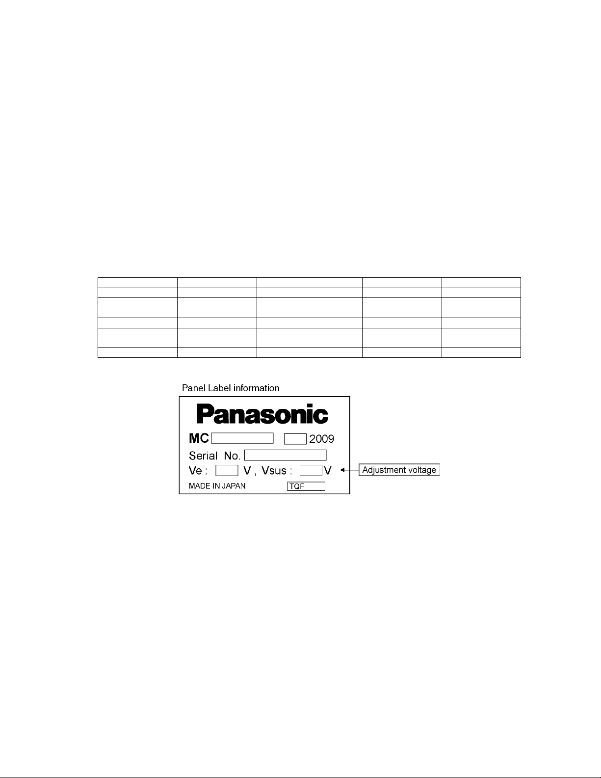
Adjust driver section voltages referring the panel data on the panel data label.
Check or adjust the following voltages with the multimeter.
Name Test Point Voltage Volume Remarks
Vsus TPVSUS (SS) Vsus ± 2V VR251 (P) *
Ve TPVE (SS) Ve ± 2.5V Fixed *
Vset TPVSET (SC) 290V ± 9V Fixed
Vad TPVAD (SC) - 175V ± 2V VR16600 (SC)
Vscn TPVSCN (SC) Vad_base : 145V ± 4V
GND_base : - 30V ± 6V
Vda TP9 (P) 60V + 1V, - 2V Fixed
Fixed
*See the Panel label.
25
Page 26
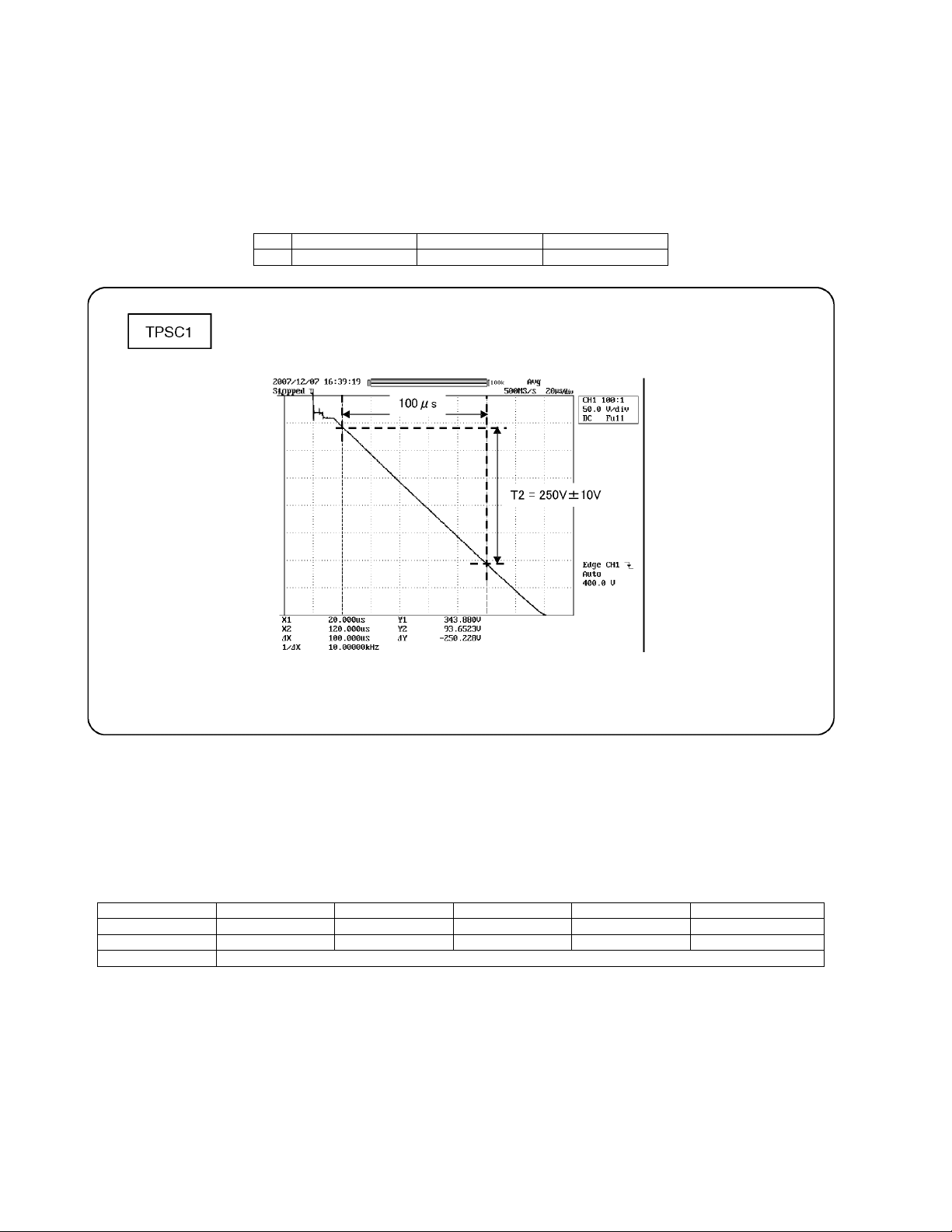
8.1.2. Initialization Pulse Adjust
1. Input the White signal to plasma video input.
2. Set the picture controls as follows.
Picture menu : Vivid
Normal : Set
Aspect : Full
3. Connect Oscilloscope to TPSC1 (SC).
Check the voltage (T2) at 100μs period on the down slop.
Test point Volume Level
T2 TPSC1 (SC) VR16601 (SC) 250 V ± 10 V
8.1.3. P.C.B. (Printed Circuit Board) exchange
8.1.3.1. Caution
1. To remove P.C.B., wait 1 minute after power was off for discharge from electrolysis capacitors.
8.1.3.2. Quick adjustment after P.C.B. exchange
Adjust the following voltages with the multimeter.
P.C.B. Name Test Point Voltage Volume Remarks
P Board Vsus TPVSUS (SS) Vsus ± 2V VR251 (P) *
SC Board Vad TPVAD (SC) - 175V ± 2V VR16600 (SC)
A Board White balance and Sub brightness for NTSC, PAL, HD, PC and 625i signals
*See the Panel label.
Caution:
Absolutely do not reduce Vsus below Ve not to damage the P.C.B.
26
Page 27
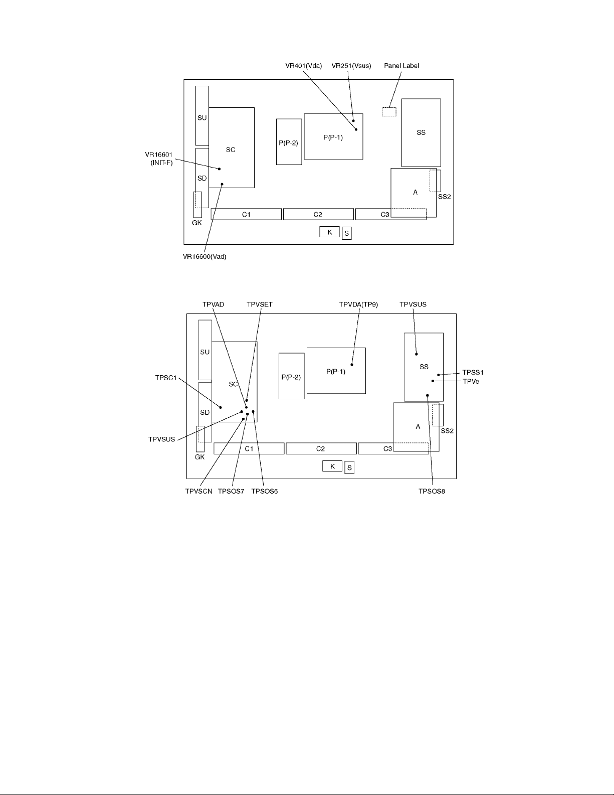
8.1.4. Adjustment Volume Location
8.1.5. Test Point Location
27
Page 28
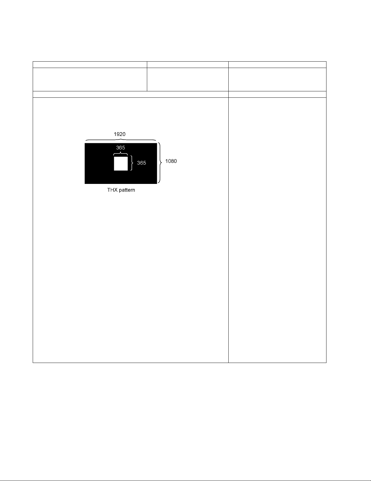
8.2. Adjustment
8.2.1. White balance adjustment
Name of measuring instrument Connection Remarks
• THX pattern
• Color analyzer
(Minolta CA-100 or equivalent)
Procedure Remarks
• Make sure the front panel to be used on the final set is fitted.
• Make sure a color signal is not being shown before adjustment.
• Put the color analyzer where there is little color variation.
1. Set the Picture menu to [cinema] and output the THX pattern.
2. Check that the color temperature is [Cool].
3. Set to serviceman mode, WB-ADJ.
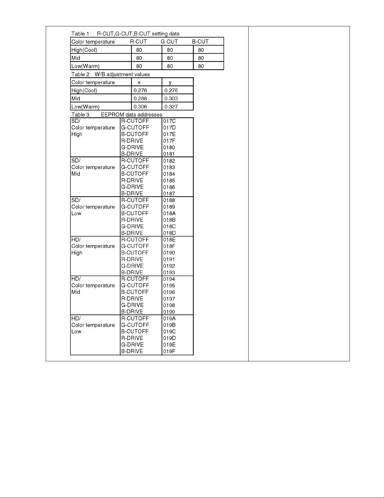
4. Set [R-CUT] [G-CUT] [B-CUT] the values written in table 1.
5. Attach the sensor of color analyzer to the center of highlight window.
6. Fix G drive at C0h and adjust [B-DRV] and [R-DRV] so x, y value of color analyzer
become the [Color temperature High] in table 2.
7. Increase RGB together so the maximum drive value in RGB becomes FC. That is,
set [ALL DRIVE] to FC.
Execute adjustment again. When that , the maximum v alue of R/G/B DRV should be FC,
and either R/G/B DRV should be FC.
8. Set color temperature to [Normal].
9. Set [R-CUT] [G-CUT] [B-CUT] the values written in table 1.
10. Attach the sensor of color analyzer to the center of highlight window.
11. Fix G drive at C0h and adjust [B-DRV] and [R-DRV] so x, y value of color analyzer
become the [Color temperature Mid] in table 2.
12. Increase RGB together so the maximum drive value in RGB becomes FC. That is,
set [ALL DRIVE] to FC.
Execute adjustment again. When that , the maximum v alue of R/G/B DRV should be FC,
and either R/G/B DRV should be FC.
13. Set color temperature to [Warm].
14. Set [R-CUT] [G-CUT] [B-CUT] the values written in table 1.
15. Attach the sensor of color analyzer to the center of highlight window.
16. Fix G drive at C0h and adjust [B-DRV] and [R-DRV] so x, y value of color analyzer
become the [Color temperature Low] in table 2.
17. Increase RGB together so the maximum drive value in RGB becomes FC. That is,
set [ALL DRIVE] to FC.
Execute adjustment again. When that , the maximum v alue of R/G/B DRV should be FC,
and either R/G/B DRV should be FC.
18. Set color temperature to [Cool].
Component input
or HDMI input
or ATSC 1080i signal
Panel surface
28
Page 29
29
Page 30

30
Page 31

HOT
(LED:8TIME)
COLD
(LED:6TIMES)
(LED:7TIMES)
(LED:4TIME)
(LED:8TIMES)
(LED:7TIMES)
(LED:4TIMES)
(LED:6TIMES)
(LED:5TIMES)
(LED:10TIMES)
(LED:2TIMES)
(LED:12TIMES)
(LED:10TIMES)
(LED:3TIMES)
(LED:12TIMES)
+3.3V(P)
F15V
+5V(P)
+3.3V(P)
VE GEN.
A25
SC20
+3.3V(P)
SOS7_SC2
VIDEO DATA
+3.3V,5V(P)
SS33
+3.3V(P)
SC-BOARD
ENEGRY RECOVERY
SOS DETECT
+3.3V(P)
C36
ON/OFF CONTROL
SOS8_SS
(LOWER)
P11
POWER MICOM
DATA
DRIVER
+3.3V(P)
CONTROL
PULSE
+3.3V(P)
VSUS
AC CORD
DATA
DRIVER
DATA
DRIVER
VAD GEN.
MAIN SW1
+5V(P)
DATA
DRIVER
SS24
SC46
VIDEO DATA
KEYSCAN1
Vda
C10
SUSTAIN
VOLTAGE
RECTIFIER
SCAN
DRIVER
P7
PROCESS
VOLTAGE
RECTIFIER
STB5V
SOS8_SS
DATA
DRIVER
SOS8_SS
VSCAN GEN.
VIDEO DATA
C21
KEYSCAN1
MAIN SW2
GK1
DATA
DRIVER
SUSTAIN CONTROL
P2
BUFFER
SS
VIDEO DATA
+5V(P)
SD46
VSUS
VIDEO DATA
C26
DATA
DRIVER
+5V(P)
SD42
DATA
DRIVER
VSUS
DATA
DRIVER
SUSTAIN CONTROL
ENERGY RECOVERY
SU41
SUSTAIN DRIVE
Vda
SOS6_SC1
Vda
A33
DATA
DRIVER
C14
SOUND15V
SS11
A6
A32
Vda
+15V(P)
P9
Vda
KEYSCAN1
VSUS
Vda
DATA
DRIVER
SCAN
DRIVER
SD11
+15V(P)
RELAY
VSUS
C22
SC2
VSET GEN.
CONNECTOR
P25
STB5V
A31
+5V(P)
+15V(P)
DATA
DRIVER
C20
SC42
STANBY
VOLTAGE
RECTIFIER
SS21
+15V(P)
+5V(P)
SOS8_SS
+5V(P)
RECTIFIER
+5V(P)
DATA
DRIVER
PS SOS4
C21
P34
P-BOARD
SOS DETECT
SUSTAIN
SUSTAIN CONTROL
DATA
DRIVER
POWER
FACTOR
CONTROL
SU11
KEY SWITCH
SC-BOARD
FLOTING PART
SOS DETECT
C33
SS-BOARD
SOS DETECT
SUSTAIN CONTROL
+15V(P)
F15V
SS2
P35
SCAN CONTROL
RECTIFIER
P6
VSUS GEN.
C35
SC41
VIDEO DATA
DATA
DRIVER
R,G,B
VIDEO SW
LVDS_I/F
STB5V
(SIDE)
BT30V
PAMEL SOS
DDR
GC6 1.8V
V,Y,C
VIDEO DATA
+1.8V(P)
SLOT
R
+3.3V(S)
VIDEO1
STB3.3V
SOS7_SC2
GC6 1.2V
ETHER_
NET IF
PANEL STATUS
DCDC
+2.5V(P)
Y/UV_16bit
+5V(P)
FLASH
OUT
A12
VIDEO2
SUB+9V DET
SUB1.8V
+5V(P)
PC
SUB9V
DIGITAL SIGNAL PROCESSOR
C.A.T.S. SENSOR
+5V(P)
HDMI1
DCDC
L,R
HDMI I/F
RECEIVER
POWER
DCDC
+3.3V(P) DET
LVDS DATA
SUB5V
SUB1.3V
+3.3V(P)
STB_D3.3V
CH,IS_I/F
SYSTEM MPU
SPEAKER(L)
SOS8_SS
OSD_16bit
SOS6_SC1
PCI BUS I/F
+3.3V(STB)
TMDS DATA
TUNER SOS DET
CIRCUIT
GC6 3.3V
REMOTE IN
V
SUB+5V DET
SOS6_SC1
EEPROM
POWER LED
EEPROM
PLASMA AI
CPG with SS
H/V Sync Control
Sub Filed Processor
Plasma AI
L,R
TMDS DATA
BT30V
PEAKS IN
PAMEL SOS
GC6
STB5V_M
SCAN CONTROL
DCDC
STB_D3.3V
RESET
+1.8V(P)
BT30V
F15V
POWER SWITCH
SD CARD DATA
KEYSCAN3
ETHERNET DATA
POWER LED(R)
CONTROL
SIGNAL
+3.3V(STB)
V
(ADAV4622)
LVDS DATA
MONITOR
OUT
SUB3.3V
+15V(P) DET
SD CARD
REMOTE RECEIVER
SUB5V
(ADV7496)
PANEL STB_ON
AUDIO I/F
STB3.3V
10BASE-T/
PANEL MICOM
+1.2V(P)
SUB9V
AMP
(SIDE)
SPEAKER(R)
SD CARD DATA
A1
MEMORY
K
L
IIC1
TUNER SOS
DCDC
RESET
10bit A/D
SUB5V
ADV7471
S
F15V
SOUND
PROCESSOR
PD3-H
L,R
Peaks-AVC
LOSD
F15V
GC6 3.3V
AUDIO SW
+2.5V(P)
F15V
S2
ON
PANEL STB_ON
SOS8_SS
REMOTE RECEIVER
100BASE-TX
HDMI2
+5V(S)
K1
KEYSCAN1
+15V(P)
ETHERNET
PANEL STATUS
+3.3V(P)
SUB1.3V
COMP1
SOUND SOS DET
CIRCUIT
DCDC
DCDC
FRONT END
PROCESSOR
TUNER SOS
DISCHARGE
CONTROL
TMDS DATA
L,R
GC6 1.2V
SUSTAIN
CONTROL
POWER SOS
A11
+1.2V(P)
SUB5V
R/G/B_36bit
SUB9V
SUB+3.3V DET
HDMI3
Y,PB,PR
CLKGEN
SOUND SOS
COMP2
SBO2
SBI2
SUB9V
OPTICAL AUDIO OUT
+9V(S)
DCDC
+5V(P)
+15V(P)
DIGITAL
VIDEO DATA
L,R
AUDIO
SUB1.8V
SWITCH
+5V(P) DET
+3.3V(P)
DCDC
SOUND SOS
DTV-SDIN
SOS7_SC2
PWM L/R
SOUND15V
A
SUB3.3V
GC6 1.8V
LOSD_OUT
DCDC
C.A.T.S. SENSOR
L,R
CH0DATA
VIDEO DATA
SOUND15V
TUNER
AUDIO
STB5V
Y,PB,PR
LED(R)
IFD_OUT
C.A.T.S. SENSOR
LVDS RX
OPTICAL
L,R
SPDIF-IN
KEYSCAN1
DDR2
Y,PB,PR
PCI BUS
LVDS DATA
+15V(P)
PANEL
MAIN ON
+15V(P)
+5V(P)
HOT
(LED:8TIME)
COLD
(LED:6TIMES)
(LED:7TIMES)
(LED:4TIME)
(LED:8TIMES)
(LED:7TIMES)
(LED:4TIMES)
(LED:6TIMES)
(LED:5TIMES)
(LED:10TIMES)
(LED:2TIMES)
(LED:12TIMES)
(LED:10TIMES)
(LED:3TIMES)
(LED:12TIMES)
DATA DRIVER (RIGHT)
POWER SUPPLY
C2C1
GK
SCAN OUT (LOWER)
SCAN OUT (UPPER)SU
SCAN DRIVE
SD
SC
KEY SWITCH
DATA DRIVER (CENTER)
P
C3
DATA DRIVER (LEFT)
9 Block Diagram
9.1. Main Block Diagram
31
Page 32

9.2. Block (1/4) Diagram
(LED:12TIMES)
JK3000
JK3701
VIDEO2
(SIDE)
VIDEO1
COMP1
COMP2
MONITOR
OUT
JK3001
PC
V2_V
V2_L
V2_R
V1_Y
V1_C
V1_V
V1_L
V1_R
D1_Y
D1_PB
D1_PR
D1_L
D1_R
D2_Y
D2_PB
D2_PR
D2_L
D2_R
MON_L
MON_R
PC_R
PC_G
PC_B
PC_H
PC_V
+5V
DDC IIC
HDMI_CEC
DDC0_IIC
+5V(HDMI) DET0
JK4502
TMDS DATA
CLOCK
DDC IIC
DDC1_IIC
+5V
HDMI_CEC
+5V(HDMI) DET1
DIGITAL SIGNAL PROCESSOR
A
IC4510
ADV7471
L/R
(ADV7496) (ADAV4622)
AUXOUT_R
AUXOUT_L
AUDIO IN
ANALOG IN
PC_HS/VS
SPDIF-IN
SDIN2
+3.3V
+3.3V
+1.8V
+1.8V
HDMI I/F RECEIVER
10bit A/D
AUDIO PROCESSOR
IIC1
IIC2
HDMI IN
DDCA_IIC
DDCB_IIC
DDCC_IIC
DDCD_IIC
+5V(HDMI) DET0
+5V(HDMI) DET1
+5V(HDMI) DET3
+5V(HDMI) DET2
DIGITAL
VIDEO OUT
SPDIF_OUT
PWM OUT
RXA
RXB
RXC
RXD
R/G/B_36bit
OPTICAL AUDIO OUT
PWM L/R
IC3001
VIDEO SW
TV
TV
V
V1
V2
D1
D2
VIDEO1
Y/C/V
VIDEO2
V
VIDEO3
VIDEO4
COMP1
Y/PB/PR
COMP2
Y/PB/PR
PC
PC
R/G/B/H/V
DTV1
Y/C
DTV
9V
AUDIO SW
TV
TV
L/R
VIDEO1
V1
L/R
VIDEO2
V2
L/R
VIDEO3
L/R
VIDEO4
L/R
COMP1
D1
L/R
COMP2
D2
L/R
PC
L/R
DTV1
L/R
5V
MAIN
OUT
MAIN L/R
RGB_CVBS
Y/PB/PR
PC_HS/VS
OUT
HS/VS
SUB MONO
L+R
MONITOR
IIC2
L/R
Y/PB/PR Y/PB/PR
HS/VS
SUB
OUT
IC2008
SUB5V
OUT
MON
L/R
3.3V +3.3V
SUB3.3V
IC4511
IC4512
+1.8V
+1.8V
DTV_R
DTV_L
OPTICAL_5.1ch
DIGITAL AUDIO
HS/VS
IC4513
SUB5V
SUB3.3V
SUB9V
SUB3.3V
SUB9V
JK4503
HDMI IN 1
TMDS DATA
CLOCK
JK4504
HDMI IN 3HDMI IN 2
TMDS DATA
CLOCK
DDC IIC
DDC2_IIC
(SIDE)
+5V
HDMI_CEC
HDMI_CEC
+5V(HDMI) DET2
BT30V
SUB5V
SUB9V
SUB3.3V
1
2
3
4
ANT IN
JK8302
SD CARD
JK8301
10BASE-T/
100BASE-TX
ETHERNET
TU8300
TUNER
VIDEO
AUDIO
BT30V
IFD_OUT1
IFD_OUT2
IF_AGC
IIC_TU
IIC2
IC8300
FRONT END
PROCESSOR
IC8302
ETHERNET IF
ETHER
NET
IC8504
EEPROM
AFT
5V
TV_V
TV_L
TV_R
BT30V
SUB5V
IF_AGC
DIGITAL
DEMODULATOR
5
GC6 RST
AFT
IIC0
IIC1
IIC2
+3.3V
+1.2V
SUB3.3V
SBI2
SBO2
CH0DATA
SD DATA:4bit
PCI BUS
IC8001
CH,IS_I/F
SD CARD
I/F
PCI BUS
I/F
Peaks-AVC
GC6 RST
IECOUT
LVDS_I/F
LOSD_OUT
DDR I/F
CPU BUS
I/F
3.3V
1.8V
1.2V
DMIX0
CLOCK
RESET
IIC3
OPTICAL_5.1ch
DIGITAL AUDIO
LVDS DATA
OSD_16bit
IC8002,03
CLOCK GEN
NOR FLASH
IIC3
DDR2
IC8004
IC8500
EEPROM
IC8502
IC8501
NAND
FLASH
SUB1.8V
SUB1.2V
3.3V
IC5110
LVDS RX
IC5607
+5V
+3.3V
IC5608
+1.8V
+1.2V
+9V
Y/UV_16bit
SUB5V
SUB3.3V
SUB1.8V
SUB1.2V
Q5691
ON/OFF
IC5401
Q5692
F15V DET
D5691
F15V
IC5700
RESET
F15V
DTV RESET
SOUND SOS
(LED:12TIMES)
Q2301
SOUND
SOS
DET
D2303
PWM L/R
SOUND15V
OPTICAL AUDIO OUT
IC2301
AUDIO AMP
SPEAKER
L_OUT
SOS
SPEAKER
R_OUT
+15V
F15V
R/G/B_36bit
Y/UV_16bit
OSD_16bit
CPU BUS
SOUND15V
D3005
OPTICAL
AUDIO
OUT
A12
L(+)
1
L(-)
A11
R(+)
R(-)
SPEAKER_L
2
1
SPEAKER_R
3
6
7
8
9
10
11
32
Page 33

9.3. Block (2/4) Diagram
(LED:2TIMES)
(LED:10TIMES)
(LED:4TIMES)
(LED:10TIMES)
(LED:3TIMES)
(LED:12TIMES)
(LED:5TIMES)
(LED:8TIMES)
(LED:6TIMES)
(LED:7TIMES)
(LED:11TIMES)
D5521
SUB9V
Q5522
P1.8V
D5613
PA5601
P1.8V
D5485
STB3.3V
STB_D3.3V
L5441
STB5V_M
P3.3V
SUB5V
P3.3V
P1.2V
D5484
D5522
P15V
P5V
BT30V
L5442
STB5V
STB3.3V
D1107
STB3.3V
SUB5V
SUB5V
F15V
SUB3.3V
D2520
F15V
ADDR/DATA
3
STB3.3V
+3.3V(P) DET
PANEL
IIC1
EEPROM
PD3-H
DIGITAL SIGNAL PROCESSOR
STB RESET
OSD I/F
RESET
+5V(P)
IC1101
15
STB RESET
+5V(P)
IC9805
2
12
IIC0
GenX8
2
PANEL STATUS
SOS6_SC1
STB
KEYSCAN1
ANALOG ASIC
VOLTAGE
PANEL STATUS
PANEL MICOM
SOUND15V
68
KEYSCAN3
SC20
IC9004
1
EEPROM
RESET
POWER ON/OFF
PANEL STATUS
1.2V
CONTROL DATA
UHZ
FLASH I/F
STB+3.3V/RESET
DROP
17
ERROR DET
6
SOUND SOS
DDR I/F
C21
P25
TUNER SOS
+1.2V
SOUND SOS
+2.5V
Config(DONE)
1.8V
+3.3V(P)
VIDEO DATA
PANEL STB_ON
AUX_ON/OFF
OSD I/F
30
PANEL
IIC2
PANEL STB_ON
A6
9
DRVRST
FPGARST
XRST
+1.8V
POWER SOS
MUTE
PANEL STB_ON
PANEL SOS
C.A.T.S. SENSOR
SCAN CONTROL
FOR
FACTORY
USE
IIC1
PANEL
IIC1
66
68
8
3.3V
2
CONTROL DATA
UHZ
3
SOS4_PS
PANEL STATUS
1
DTV5V
IC9808
PANEL SOS
DTV RESET
F15V
SOS7_SC2
+15V(P)
IC9807
SUB9V
60
29
SUB9V
3.3V
9
PANEL SOS
SUB3.3V DET
F15V
IIC3
1
STB_RESET
A25
7
SUB5V
KEYSCAN3
IC9001
SUB5V
TV SUB ON
A32
EEP_
IIC1
+15V(P) DET
66
DTV RESET
DRV
F15V
SOUND15V
A1
VIDEO DATA
GenX7
EEP_
IIC1
IIC3
SUSTAIN CONTROL
11
A17
10
IC9902,03
+5V(P) DET
*PLASMA AI
*CPG with SS
*H/V Sync Control
*Sub Filed Processor
*Plasma AI
+3.3V(P)
SUB5V
+5V(P)
TV SUB ON
SBO2
+15V(P)
4
SOS8_SS
P7
VIDEO DATA
A18
IC5606
13
HDMI_CEC
SCAN CONTROL
PANEL SOS
AFT
AFT
+3.3V(P)
IIC3
63
IC9303
STB_D3.3V
TUNER SOS
14
IIC1
2.5V
POWER LED(R)
9
IIC2
STB3.3V
STB5V
DDR2
IC9806
IC9300
TUNER SOS
IIC1
FLASH
MEMORY
+15V(P)
SUB9V DET
BT30V
VIDEO DATA
SOS8_SS
1
SUB9V
45
DISCHARGE CONTROL
BT30V
STB_RESET
HDMI_CEC
+15V(P)
CONTROL DATA
A33
6
SOS6_SC1
+5V(P)
P6
TV SUB ON
5
FOR
FACTORY
USE
XRST,
XRSTSYS
SUSTAIN CONTROL
A31
STB5V
A
SUB5V DET
+3.3V
SOS7_SC2
14
PANEL MAIN ON
REMOTE IN
SUB3.3V
TEMP SENSOR
STB
+3.3V
IC9003
LVDS DATA
C22
Config(DONE)
+3.3V
SOUND15V
IC5480
Config(CCLK,DDTATA,PROGB),
FPCLK,FPDATA[1:0],FVSEL
KEYSCAN1
TV SUB ON
KEYSCAN3
SBI2
IC1100
IC4800
37
PANEL_MAIN_ON
1.2V
D5486
RESET
F15V
IC5851
DDR I/F
GC6+3.3V
+1.2V
IC5100
+3.3V
+1.2V
GC6
+1.8V
EXB BUS
CPU BUS
GC6+1.2V
GC6 RST
R/G/B_36bit
GC6+1.8V
+1.8V
D5615
D5614
Y/UV_16bit
OSD_16bit
LVDS DATA
PANEL
IIC2
PANEL
IIC2
IC9500
+3.3V
PORT-C
PORT-A
LOSD
GC6 RST
LVDS
DDR2
IC5001,02
BT30V
CPU BUS
R/G/B_36bit
Y/UV_16bit
OSD_16bit
SOUND15V
DDC0,1,2_IIC
DDC_IIC
HDMI_CEC_
PU_ON
F15V
IC5300
+3.3V
FAN SOS
FAN MAX
FAN ON
FAN ON
FAN SOS
FAN MAX
3
11
1
4
2
8
5
10
9
6
7
SYSTEM MPU
+5V(HDMI)
DET 0,1,2
+5V(HDMI)DET 0,1,2
CLK BUFFER
IC5201
6
POWER LED
REMOTE IN
STB+3.3V
1
S
REMOTE
RECEIVER
KEYSCAN3
PC2501
10
RM2501
C.A.T.S.
SENSOR
K
AI SENSOR
SW2500
S2
1
R_LED_ON
2
REMOTE RECEIVER
SUB+5V
KEYSCAN3
5
POWER SWITCH
ON
K1
9
2
K1
POWER LED
8
C.A.T.S.
3
POWER SWITCH
(LED:2TIMES)
(LED:10TIMES)
(LED:4TIMES)
(LED:10TIMES)
(LED:3TIMES)
(LED:12TIMES)
(LED:5TIMES)
(LED:8TIMES)
(LED:6TIMES)
(LED:7TIMES)
(LED:11TIMES)
33
Page 34

9.4. Block (3/4) Diagram
HOT
(LED:4TIMES)
HOT COLD
COLD
HOT
COLD
HOT COLD
POWER SUPPLY
P
DC(+)
65
P52
12
P51
L601
L602
FILTER
L603
F602 F601
10A 250V
LIVE
L604,L605
D603,D607
RECTIFIER
1
2
2A 250V
F501
RECTIFIER
LIVE
NEUTRAL
10A 250V
NEUTRAL
P9
AC CORD
D506
RF601
Q608
Q601,Q602
IC601
Q603-Q606
PFC CONTROL
K602
K601
K603
COLD
HOT
NEUTRAL
PHOTO COUPLER
PHOTO COUPLER
PHOTO COUPLER
PHOTO COUPLER
PHOTO COUPLER
D505
PHOTO COUPLER
Q502,Q505,Q506
AC DET
HOT COLD
T201
PC201
PC202
T301
PC301
PC302
HOT COLD
PC501
T501
PC4
PHOTO COUPLER
D551
P2
Vsus
D254-D257
IC251
Vsus
ERROR DET
D401
D402
D352
IC352
+15V
ERROR DET
IC551
STB
ERROR DET
PC3
HOT
COLD
BIAS_ON
RUSH RELAY_ON
Vsus
VR251
PC401
Vda_ON
Vsus_ON
MULTI_ON
POWER MICOM
MAIN RELAY_ON
AC DET
+5V
MC401
Vda
CONTROL
PHOTO
COUPLER
IC701
MAIN SW_ON
STB_ON
VR401
Q401
Q353
15V_OUT
Vda_OUT
15V_ON
Vsus_OUT
(LED:4TIMES)
POWER SOS
PANEL_MAIN_ON
ALL_OFF
TV SUB ON
STB_OUT
Vda
5V_ON
Q402
Q403
Q551
FSTB+15V
1 5
3
P34
7
9
P6
A6
FSTB+15V
FSTB+15V
1
+15V(SND)
15V
+15V(SND)
3
+15V(SND)
Q351
MC451
+5V(STB)
P7
A6
1
+5V
+15V(P)
Vda
+5V(P)
2
+15V(P)
+15V(P)
10
+5V(P)
6
+5V(STB)
TV SUB ON
8
ALL_OFF
1
Vsus
P11
1
Vsus
4
+15V(P)
P35
1
Vda
2
Vda
P25
1
+15V(P)
2
+15V(P)
5
+5V(P)
6
+5V(P)
9
+5V(STB)
12
SOS4_PS
11
PANEL_MAIN_ON
SC2
SS11
C35
A25
5A 250V
Q201,Q202
F201
RESONANCE
IC201
Vsus
POWER
CONTROL
5A 250V
Q301,Q302
F301
RESONANCE
IC301
MULTI
POWER
CONTROL
BIAS_ON
BIAS(+)
P56
P55
DC(+)
1
1
P58
P57
3
3
1
1
P53
121
P54
2
LIVE
RUSH RELAY
MAIN RELAY
IC501
STB
CONTROL
34
Page 35

(LED:8TIMES)
(LED:7TIMES)
(LED:6TIMES)
TPVE
D16280
TPSS1
TPVSUS
D16255
TPSOS8
D16282
D16253
D16920
D16480
D16821
D16721
VF_GND
TPVAD
D16791
5V
TPSC1
D16583
D16493
D16820
TPVSUS
TPSOS6
D16901
5V
TPSOS7
D16473
VR16601
TPVSET
D16725
VR16600
TPVSCN
SS
33
59
Q16051
PLASMA PANEL
BUFFER
A31
D16053
CB8
Vda
SUSTAIN CONTROL
Q16023
1
DATA DRIVER (CENTER)
D16052
7
IC16312
SUSTAIN CONTROL
1
KEYSCAN1
1
C35
CB9
C2
IC16241
IC17201
CB4
UML
CB
15
USL
CB
11
FPC DET
Q16280
C3
30
55
CB5
DRIVER
52
VIDEO DATA
Vda
PLASMA PANEL
SS
11
DATA DRIVER (LEFT)
Vda
KEY SWITCH
1
ELECTRODE
DATA DRIVER (RIGHT)
Q16022
SUSTAIN CONTROL
1
ERROR DET
DRIVER
C33
+15V
4
VSUS Gen.
2
9
CB
14
2
RECOVERY
1
LED(G)
Q16041
6
C1
CB
13
41
C10
C21
Q16004
68
+5V(P)
1
ENERGY
SOS8_SS
ERROR DET
UMH
USH
IC16251
SS
56
CB6
UEH
REG.
C20
Q16021
CB7
IC16131
44
UML
(LOWER)
Q16101
IPD CIRCUIT
SOS8_SS
SS
58
C33
SS2
25
PANEL SUSTAIN
P11
CB3
Vda
BUFFER
P35
SHUNT
VIDEO DATA
6
2
PC16301
7
2
VIDEO DATA
CB
12
IC16304
VE GEN.
+5V(P)
CONTROL DATA
USH
CB2
13
7
1
PC16191
PHOTO
COUPLER
SS
21
12
Q16001
UEH
GK
1
Q16002
+5V(P)
USL
4
SS
24
13
7
Q16102
CONTROL DATA
SS33
SS
55
15
SS
IC16151
SUSTAIN DRIVE
Vsus
CONNECTOR
13
2
+3.3V(P)
PANEL DRIVER
1
SUSTAIN
1
1
PANEL DRIVER
SS
53
13
UMH
3
+3.3V(P)
D16041
PANEL DRIVER
VE Gen.
D16042
CIS
4
PC16684
22
5
2
SD
42
CPH2
SC
CPH1
SCAN OUT (UPPER)
+5V
Q16608
IC16501
(SC1)
SU
CLK
+5V(P)
Q16607
SCAN OUT (LOWER)
VSET23
GEN.
A33
PC16480
SD
8
CEL
VSET23
LED(G)
4
IC16725
(VAD)
6
Vfo
D16482
VHIZ GEN.
Q16661
IC16464,65
3
D16481
SC
41
CRC2
VSET23
(SC2)
35
8
CIS
21
6
SU
41
DRIVER
IC16771
LOGIC IC
D16860
SCAN
CMH
DRIVER
8
IC16786,87
SCAN
CML
Q16451
SHUNT
SC2
15V_F
OC2
4
REG.
Q16604
VHIZ
COMPARATOR
OC2
CSL
SOS7_SC2
IC16692
Q16404
Q16403
IC14801-04
Q16876
Q16621
3
F_5V_B
Vscn
IC16563
+15V(P)
CLK
D16871
PHOTO COUPLER
VSCN-F
FOR
FACTORY
USE
VHIZ
9
SOS6_SC1
CMH
Q16424
7
VSET GEN.
SHUNT REG
SC
42
SC
20
IPD CIRCUIT
Q16402
Q16490
9
VAD
Q16422
COMPARATOR
CIRCUIT
UHZ
CERS
GEN.
SEPA PROTECT
IPD CIRCUIT
IC14805-08
CSL
BUFFER
Q16601
SHUNT REG
+15V(P)
SCAN CONTROL
CML
VSCN GEN.
15V_F
CRC2
DROP
SCAN
CONTROL
CEL
CERS
8
SEL
VOLTAGE
CERS
CRC1
SU
11
16V-F
CPH1
DC/DC
INVERTER
ERROR DET
IC14605-08
2
D16859
IC14601-04
SIU
ERROR DET
1
IC16521
Q16818
OC1
MAIN_STOP
IC16792
IC16793
D16461
CSH
SC
46
IC16581
(INIT-F)
PC16601
VSCN
SCAN
Q16441
+5V
SIU
SCAN
D16462
DRIVER
CSH
DRIVER
SD
11
PANEL SCAN
SCNR_PRO
PLASMA PANEL
ELECTRODES
PC16603
PHOTO COUPLER
CSL
CONVERTER
(15V_F)
PHOTO COUPLER
F_5V_A
INVERTER
SEL
SCAN DRIVE
PHOTO COUPLER
PHOTO COUPLER
IC16791
INVERTER
1
P2
CML
CSH/CMH GATE
DRIVE CIRCUIT
Vsus
CPH2
SD
46
CSL/CML GATE
DRIVE CIRCUIT
VOH
PC16685
PHOTO
IC16490,91
VOL
COUPLER
SC50
IC14901-05
ERROR DET
5
2
Vfo
IC16661
IC16561,62
Q16423
IC16784
2
19
6
SCNR_PRO
Q16622
IC16773
4
1
UHZ
CRC1
PC16461
OC1
IC16920
IC16724
SU1B-SU5B
SD1B-SD5B
CB1
GK1
KEY SWITCH
1
C14
KEYSCAN1
1
155
10
C36
59
5
SOS8
681
CONTROL DATA
64
30
VIDEO DATA
Vda
39
C26
+5V(P)
Vda
6
+5V(P)
SOS8_SS
C22
+3.3V(P)
1
CONTROL DATA
32453
A32
VIDEO DATA
SUSTAIN CONTROL
SUSTAIN CONTROL
60 9
CB
10
Q16442
D16463
Q16452
Q16623
D16483
IC17203
BUFFER
IC17202
BUFFER
5566
VIDEO DATA
KEYSCAN1
IC16564
IC16801
IPD CIRCUIT
IC16788,89
IC16691
NAND GATE
Vad+5V
Q16024
Q16052
Q16042
D16043
D16051
+3.3V(P)
(LED:8TIMES)
(LED:7TIMES)
(LED:6TIMES)
9.5. Block (4/4) Diagram
35
Page 36

36
Page 37

10 Wiring Connection Diagram
10.1. Caution statement.
Caution:
Please confirm that all flexible cables are assembled correctly.
Also make sure that they are locked in the connectors.
Verify by giving the flexible cables a very slight pull.
10.2. Wiring (1)
37
Page 38

10.3. Wiring (2)
38
Page 39

10.4. Wiring (3)
39
Page 40

10.5. Wiring (4)
40
Page 41

10.6. Wiring (5)
41
Page 42

42
Page 43

11 Schematic Diagram
11.1. Schematic Diagram Note
43
Page 44

11.2. P(P-1)-Board (1/2) Schematic Diagram
TO
P(P-2)-BOARD
(P51)
A
B
C
D
PFC
E
F
P(P-1)-BOARD ETX2MM761MGN (1/2)
!
2 896
4
5
CONTROL
731
44
Page 45

11.3. P(P-1)-Board (2/2) Schematic Diagram
13 1410 1716 181211 15
COLD
HOT
COLD
HOT
COLD
HOT
TO
A-BOARD
(A6)
TO
A-BOARD
(A6)
TO
A-BOARD
(A25)
TO
C3-BOARD
(C35)
TO
SC-BOARD
(SC2)
TO
SS-BOARD
(SS11)
TO
P(P-2)-BOARD
(P55)
TO
P(P-2)-BOARD
(P53)
TO
P(P-2)-BOARD
(P57)
!
P(P-1)-BOARD ETX2MM761MGN (2/2)
Vsus POWER
CONTROL
COMPARATOR
Vda
CONTROL
MULTI
CONTROL
POWER
Vsus
ERROR DET
+5V(P)
POWER MICOM
STB CONTROL
STB
ERROR
DET
+15V
ERROR
DET
Vda
Vsus
45
Page 46

11.4. P(P-2)-Board Schematic Diagram
A
TO
P(P-1)-BOARD
(P58)
P(P-2)-BOARD ETX2MM761MGN
!
COLD
B
HOT
COLD
HOT
TO
P(P-1)-BOARD
(P52)
C
D
TO
P(P-1)-BOARD
(P56)
E
TO
P(P-1)-BOARD
(P54)
F
2 896
4
5
731
46
Page 47

11.5. GK, K and S-Board Schematic Diagram
VCC
GND
OUT
PUSH
C2522
0.1u
16V
C2512
6.3V
10u
D2520
LN1271RALTR
D2512
MAZ80430LL
PC2501
B3JB00000046
RM2501
B3RAD0000160
Q2510
2SD0601A0L
Q2511
2SD0601A0L
R2524
22k
R2517
47
R2542
47k
R2513
5.6k
R2557
5.6k
R2525
820
R2520
220k
R2516
22k
K1
123456789
10
FL2500
J0MAB0000201
12
R3765
0
SW3763A
EVQ23405R
R3772
1.74k
R3771
21k
SW3759A
EVQ23405R
R3775
3.16k
R3773
1.62k
SW3764A
EVQ23405R
SW3762A
EVQ23405R
SW3765A
EVQ23405R
C3752
1000p
50V
GK1
1
2
R3774
2.32k
SW3761A
EVQ23405R
SW2500
K0F122A00172
S2
1
2
REMOTE RECEIVER
C.A.T.S. SENSOR
POWER LED
GND
STB3.3V
SUB5V
RM_IN
GND
KEYSCAN3(IN)
C.A.T.S._SENSOR
R_LED_ON
SUB5V
R_LED_ON
STBY3.3V
C.A.T.S.SENSOR
REMOCON
KEY3
GND
KEYSCAN3(OUT)
KEYSCAN
VOL.DN CH.DN CH.UP INPUT/OK
MENU
VOL.UP
GND
GK-BOARD TNPA4874S
!
K-BOARD TNPA4871S
!
A
F
5
B
42
D
3681 7
C
E
9
POWER SW
S-BOARD TNPA4873S
!
TO
C1-BOARD
(C14)
TO
A-BOARD
(A1)
47
Page 48

11.6. A-Board (1/22) Schematic Diagram
A-BOARD TXN/A1DVUUS (1/22)
!
Peaks-AVC,DDR
A
TO 17/22
TO 9/22
VDD3.3V
IC8001 A26 VDD33
IC8001 AC4 VDD33
IC8001 AD4 VDD33
IC8001 AE8 VDD33
IC8001 AF7 VDD33
IC8001 AG6 VDD33
IC8001 AG11 VDD33
IC8001 AG12 VDD33
IC8001 AG15 VDD33
IC8001 AG16 VDD33
IC8001 AH5 VDD33
IC8001 AJ4 VDD33
IC8001 AK3 VDD33
IC8001 B26 VDD33
IC8001 C26 VDD33
IC8001 D7 VDD33
IC8001 D8 VDD33
IC8001 D15 VDD33
IC8001 D16 VDD33
IC8001 D19 VDD33
IC8001 D20 VDD33
IC8001 D23 VDD33
IC8001 D24 VDD33
IC8001 D26 VDD33
IC8001 F25 VDD33
IC8001 G4 VDD33
IC8001 H4 VDD33
IC8001 M4 VDD33
IC8001 L4 VDD33
IC8001 R4 VDD33
IC8001 T4 VDD33
IC8001 W4 VDD33
IC8001 Y4 VDD33
IC8001 E26 VDD33
B PORT
(Sub Video Input or Address)
VI2P12
VI2P13
VI2P14
VI2P15
VI2P16
VI2P17
VI2P18
VI2P19
TO 3/22
VI2P22
VI2P23
VI2P24
VI2P25
SUB3.3V
VI2P26
VI2P27
VI2P28PCAD6
VI2P29
R8109
2.2k
TO 15/22
VI2CLK
R8114
10k
Analog Video I/F
TO 7/22
VDD3.3V
MVDACO1
MVDACO2
R8098
0
R8005
10k
IC8001 F24 SBI0
SBI0
IC8001 B25 SBO0
SBO0
IC8001 AK10 SMTCMD1
R8115
IC8001 AE11 SMTSEL1
10k
SBI2
IC8001 C25 SBI2
IC8001 E25 SBO2
SBO2
IC8001 G6 VI2P4
IC8001 M3 VI2P12
IC8001 M6 VI2P13
IC8001 M2 VI2P14
IC8001 N5 VI2P15
IC8001 N6 VI2P16
IC8001 N3 VI2P17
IC8001 P6 VI2P18
IC8001 N2 VI2P19
IC8001 P2 VI2P22
IC8001 R6 VI2P23
IC8001 P1 VI2P24
IC8001 R3 VI2P25
IC8001 R2 VI2P26
IC8001 R5 VI2P27
IC8001 R1 VI2P28
IC8001 T1 VI2P29
IC8001 L3 VI2HSYNC
IC8001 L6 VI2VSYNC
IC8001 M1 VI2CLK
IC8001 E10 MVDACO1
IC8001 D9 MVDACO2
R8004
24k
C8003
10V
R8006
1u
C8005
10V
1u
SBI1
SBO1
RXD2
TXD2
A1 VSS
IC8001
IC8001 A2 VSS
IC8001 A3 VSS
IC8001 A8 VSS
IC8001 AA4 VSS
IC8001 AA27 VSS
IC8001 AB4 VSS
IC8001 AB29 VSS
IC8001 AC25 VSS
IC8001 AC28 VSS
IC8001 AD27 VSS
IC8001 AE6 VSS
IC8001 AE7 VSS
IC8001 AE19 VSS
IC8001 AE22 VSS
IC8001 AE26 VSS
IC8001 AE29 VSS
IC8001 AF6 VSS
IC8001 AF13 VSS
IC8001 AF14 VSS
IC8001 AF19 VSS
IC8001 AF21 VSS
IC8001 AF25 VSS
AF27 VSS
IC8001
IC8001 AG5 VSS
IC8001 AG9 VSS
IC8001 AG10 VSS
IC8001 AG13 VSS
IC8001 AG14 VSS
IC8001 AG19 VSS
IC8001 AG20 VSS
IC8001 AG24 VSS
IC8001 AG29 VSS
IC8001 AH4 VSS
IC8001 AH11 VSS
IC8001 AH13 VSS
IC8001 AH15 VSS
IC8001 AH19 VSS
IC8001 AH23 VSS
IC8001 AH27 VSS
IC8001 AH30 VSS
IC8001 AJ3 VSS
IC8001 AJ29 VSS
IC8001 AK1 VSS
IC8001 AK2 VSS
IC8001 AJ13 VSS
IC8001 AJ16 VSS
IC8001 AJ19 VSS
IC8001 AJ22 VSS
PORT6[4]
PORT6[5]
PORT6[7]
IC8001 B9 VVREF
IC8001 F10 MVIREF
24k
IC8001 C9 VCOMP
EA24
EA08
EA09
EA10
EA11
EA12
EA13
EA14
EA15
EA16
EA17
EA18
EA19
EA20
EA21
EA22
EA23
(DDR_SEL)
(GC6_XRST)
V
U
C
Y
Y
Cmp
Cmp
IC8001 AJ26 VSS
IC8001 AK13 VSS
IC8001 AK19 VSS
IC8001 AK25 VSS
IC8001 AK28 VSS
IC8001 B1 VSS
IC8001 B2 VSS
IC8001 B3 VSS
IC8001 B8 VSS
IC8001 C3 VSS
IC8001 C8 VSS
IC8001 C10 VSS
IC8001 C13 VSS
IC8001 C18 VSS
IC8001 D4 VSS
IC8001 D10 VSS
IC8001 D12 VSS
IC8001 D17 VSS
IC8001 D18 VSS
IC8001 D21 VSS
IC8001 D22 VSS
IC8001 E5 VSS
IC8001 F6 VSS
IC8001 F9 VSS
IC8001 G7 VSS
IC8001 J4 VSS
IC8001 K4 VSS
IC8001 M5 VSS
IC8001 M12 VSS
IC8001 M13 VSS
IC8001 M14 VSS
IC8001 M15 VSS
IC8001 M16 VSS
IC8001 M17 VSS
IC8001 M18 VSS
IC8001 M27 VSS
IC8001 N4 VSS
IC8001 N12 VSS
IC8001 N13 VSS
IC8001 N14 VSS
IC8001 N15 VSS
IC8001 N16 VSS
IC8001 N17 VSS
IC8001 N18 VSS
IC8001 N19 VSS
IC8001 N29 VSS
IC8001 P4 VSS
IC8001 P12 VSS
IC8001 P13 VSS
IC8001 Y1 EA0
EA0
IC8001 W6 EA1
EA1
IC8001 W5 EA2
EA2
IC8001 Y2 EA3
EA3
TO 3/22
TO 3/22
TO 3/22
TO 3,15/22
R
B
G
Cmp
TO 3/22
TO 14/22
TO 3/22
TO 3/22
TO 14/22
TO 13/22
TO 4/22
EA4
EA5
EA6
EA7
ED0
ED1
ED2
ED3
ED4
ED5
ED6
ED7
ED8
ED9
ED10
ED11
ED12
ED13
ED14
ED15
XERE
XEWE0
XEWE1
XECS2
XECS4
XECS6
XECS7
XIRQ1
XIRQ2
XIRQ3
A_XRST
XEDK
IC8001 Y5 EA4
IC8001 Y3 EA5
IC8001 AA1 EA6
IC8001 AA2 EA7
IC8001 Y6 ED0
IC8001 AA3 ED1
IC8001 AB1 ED2
IC8001 AA5 ED3
IC8001 AB2 ED4
IC8001 AB3 ED5
IC8001 AC1 ED6
IC8001 AA6 ED7
IC8001 AB5 ED8
IC8001 AB6 ED9
IC8001 AC2 ED10
IC8001 AD1 ED11
IC8001 AC3 ED12
IC8001 AD2 ED13
IC8001 AE1 ED14
IC8001 AE2 ED15
IC8001 AC5 XERE
IC8001 AE3 XEWE0
AF3 XEWE1
IC8001
IC8001 AC6 XEDK
IC8001 AF2 ERXW
IC8001 AF1 ECLK
IC8001 AD3 ESZ0
IC8001 AG1 ESZ1
IC8001 AD5 XECS0
IC8001 AG2 XECS1
IC8001 AD6 XECS2
IC8001 AG3 XECS4
IC8001 AH2 XECS6
IC8001 AH3 XECS7
IC8001 U2 XNMIRQ
IC8001 U5 XIRQ1
IC8001 U3 XIRQ2
IC8001 V1 XIRQ3
IC8001 AG28 BOOTSWAP
IC8001 D25 XRST
BOOTROM CS
SCARD CS
EAS
PORT14[1]
1394_CS
(SCARD_NMIRQ)
(SCARD_IRQ)
(FE_IRQ)
(HDMI_IRQ)
CH,IS IF
CH0CLK
CH0VAL
TO 14/22
CH0PSYNC
CH0DATA
R8696
TO 17/22
R8716
47k
R8653
10k
IS0VAL
10k
IC8001 P14 VSS
IC8001 P15 VSS
IC8001 P16 VSS
IC8001 P17 VSS
IC8001 P18 VSS
IC8001 R13 VSS
IC8001 R14 VSS
IC8001 R15 VSS
IC8001 R16 VSS
IC8001 R17 VSS
IC8001 R18 VSS
IC8001
R26 VSS
IC8001
R28 VSS
IC8001 T13 VSS
IC8001 T14 VSS
IC8001 T15 VSS
IC8001 T16 VSS
IC8001 T17 VSS
IC8001 T19 VSS
IC8001 T29 VSS
IC8001 U4 VSS
IC8001 U16 VSS
IC8001 U17 VSS
IC8001 U26 VSS
IC8001 V4 VSS
IC8001 V16 VSS
IC8001 V18 VSS
IC8001 V27 VSS
IC8001 W16 VSS
IC8001 W19 VSS
IC8001 W28 VSS
W30 VSS
IC8001
IC8001 Y26 VSS
IC8001 AH29 FPENF
LVDS I/F
B
TO 15/22 TO 3/22 TO 10/22
TA1N
TA1P
TB1N
TB1P
TC1N
TC1P
TCLK1N
TCLK1P
TD1N
TD1P
IC8001 B27 TA1N
IC8001 A27 TA1P
IC8001 B28 TB1N
IC8001 A28 TB1P
IC8001 B29 TC1N
IC8001 B30 TC1P
IC8001 C29 TCLK1N
IC8001 C30 TCLK1P
IC8001 D29 TD1N
IC8001 D30 TD1P
IC8001 E29 TE1N
IC8001 E30 TE1P
IC8001 F29 TA2N
IC8001 F30 TA2P
IC8001 G29 TB2N
IC8001 G30 TB2P
IC8001 H29 TC2N
IC8001 H30 TC2P
IC8001 J29 TCLK2N
IC8001 J30 TCLK2P
IC8001 K29 TD2N
IC8001 K30 TD2P
IC8001 L29 TE2N
IC8001 L30 TE2P
USB I/F
IC8001 B13 XO
IC8001 A13 XI
IC8001 A10 USBDP
IC8001 B10 USBDN
C
SUB1.2V
L8011
J0JHC0000045
IC8001 F14 VDDUSB
C8083
C8084
16V
50V
0.1u
SUB3.3V
J0JHC0000045
D
J0JHC0000045
E
F
1000p
L8012
L8013
IC8001
C8069
1000p
16V
F11 VDDAUSB
50V
IC8001 C11 VDDPUSB
C8082
50V
1000p
IC8001 D11 VSSPUSB
IC8001 E11 VSSAUSB
IC8001 E14 VSSUSB
IC8001 B11 USBRREF
IC8001 A11 USBATEST
IC8001 T18 DPAVDD
IC8001 V2 M1A1AVDD
IC8001 U6 M1A1AVSS
IC8001 M25 V2AVDD
IC8001 N25 V2AVSS
IC8001 G25 LVVDD33
IC8001 H25 LVVDD33
IC8001 J25 LVVDD33
IC8001 K25 LVVDD33
IC8001 L25 LVVDD33
C8085
16V
0.1u
C8067
16V
0.1u
C8081
16V
0.1u
R8107
6.2k
R8106
10k
SUB3.3V
L8009
J0JHC0000045
C8072
16V
0.1u
C8073
16V
0.1u
C8074
16V
0.1u
SUB3.3V
L8008
J0JHC0000045
C8070
16V
0.1u
C8071
0.1u
PCI BUS I/F
PCRST
IC8001 E16 PCRST
IC8001 B16 PCIDSELA
PCIDSELA
IC8001 C17 PCCLKO0
PCCLKO0
IC8001 F17 PCCXBE0
PCCXBE0
IC8001 B17 PCCXBE1
PCCXBE1
IC8001 E17 PCCXBE2
PCCXBE2
IC8001 A17 PCCXBE3
PCCXBE3
IC8001 A25 PCAD0
PCAD0
IC8001 E24 PCAD1
PCAD1
IC8001 C24 PCAD2
PCAD2
IC8001 B24 PCAD3
PCAD3
IC8001 F23 PCAD4
PCAD4
PCAD5
IC8001 A24 PCAD5
IC8001 C23 PCAD6
IC8001
B23 PCAD7
PCAD7
IC8001 E23 PCAD8
PCAD8
IC8001 A23 PCAD9
PCAD9
IC8001 F22 PCAD10
PCAD10
IC8001 C22 PCAD11
PCAD11
IC8001 B22 PCAD12
PCAD12
PCAD13
IC8001 A22 PCAD13
IC8001 E22 PCAD14
PCAD14
IC8001 C21 PCAD15
PCAD15
IC8001 F21 PCAD16
PCAD16
IC8001 B21 PCAD17
PCAD17
IC8001 E21 PCAD18
PCAD18
IC8001 A21 PCAD19
PCAD19
IC8001 F20 PCAD20
PCAD20
IC8001 C20 PCAD21
PCAD21
IC8001 E20 PCAD22
PCAD22
IC8001 B20 PCAD23
PCAD23 XECS0
IC8001 A20 PCAD24
PCAD24
IC8001 C19 PCAD25
PCAD25
IC8001 B19 PCAD26
PCAD26
PCAD27
IC8001 F19 PCAD27
IC8001 A19 PCAD28
PCAD28
PCAD29
IC8001 E19 PCAD29
IC8001 B18 PCAD30
PCAD30
PCAD31
IC8001 F18 PCAD31
IC8001 F15 PCXSERR
PCXSERR
IC8001 B15 PCXPERR
PCXPERR
IC8001 C15 PCXSTOP
PCXSTOP
IC8001 A15 PCXFRAME
PCXFRAME
IC8001 A14 PCXTRDY
PCXTRDY
IC8001 E15 PCXIRDY
PCXIRDY
IC8001 C16 PCDEVSEL
PCDEVSEL
IC8001 A16 PCPAR
PCPAR
IC8001 F16 PCIRQ0
PCIRQ0
IC8001 E18 PCBRQ0
PCBRQ0
IC8001 A18 PCBGT0
PCBGT0
SUB1.2V
L8004
J0JHC0000045
C8007
IC8001 R19 VDDR
16V
VDD3.3V
0.1u
IC8001 U19 VDDR
IC8001 V17 VDDR
IC8001 W18 VDDR
C8008
IC8001 AE18 VDDR
16V
0.1u
IC8001 AF18 VDDR
IC8001 AG18 VDDR
IC8001 AH18 VDDR
C8010
IC8001 AJ18 VDDR
10V
10u
IC8001 AK18 VDDR
R8007
0
IC8001 A9 DAAVSS1
IC8001 E9 DAAVDD1
C8034
16V
0.1u
C8033
16V
0.1u
C8006
IC8001 P19 VDDA
16V
0.1u
IC8001 V19 VDDA
C8009
IC8001 W17 VDDA
10V
10u
IC8001 A29 LVVSS
IC8001 A30 LVVSS
IC8001 C28 LVVSS
IC8001 D27 LVVSS
D28 LVVSS
IC8001
IC8001 E27 LVVSS
IC8001 E28 LVVSS
IC8001 F26 LVVSS
F27 LVVSS
IC8001
IC8001 F28 LVVSS
IC8001 G26 LVVSS
IC8001 G27 LVVSS
IC8001 G28 LVVSS
IC8001 H26 LVVSS IC8001 U15 VDD12
IC8001 H28 LVVSS
IC8001 J26 LVVSS
IC8001 J27 LVVSS
IC8001 J28 LVVSS
IC8001 K26 LVVSS
IC8001 K27 LVVSS
IC8001 K28 LVVSS
IC8001 L26 LVVSS
IC8001 L27 LVVSS
IC8001 L28 LVVSS
LOSD OUT (for HQ1)
SLRCK
DSRCK
ADCCK
LCSCK
VI1CVBS3
VI1CVBS2
VI1CVBS1
VI1CVBS0
VI1CK204F
VI1CK208F
VOUTENB
IIC I/F
SCL0
SDA0
SCL1
SDA1
SBT2
SBT0 VI1P20
XECS5
XECS3
SD CARD I/F
SDCLK
SDCD
SDCMD
SDDAT0
SDDAT1
SDDAT2
SDDAT3
SDWP
VI2P6
VI2P5
ADIN
LCSID
VI2P0
VI2P1
VI2P2
VI2P3
VI2P7
VI2P8
VI2P9
IC8001 T2 SCL0
IC8001 T3 SDA0
IC8001 T6 SCL1
IC8001 U1 SDA1
IC8001 AK7 SBT2
IC8001 AH8 SBT0
IC8001 AE4 XECS5
IC8001 AH1 XECS3
IC8001 J5 VI2P6
IC8001 D14 SLRCK
IC8001 G5 VI2P5
IC8001 F13 DSRCK
IC8001 D13 ADCCK
IC8001 E13 ADIN
IC8001 C14 LCSID
IC8001 B14 LCSCK
IC8001 E8 VI1CVBS3
IC8001 C7 VI1CVBS2
IC8001 E7 VI1CVBS1
IC8001 F7 VI1CVBS0
IC8001 D6 VI1CK204F
IC8001 D5 VI1CK208F
IC8001 C4 VI2P0
IC8001 E4 VI2P1
IC8001 F5 VI2P2
IC8001 F4 VI2P3
IC8001 J6 VI2P7
IC8001 G2 VI2P8
IC8001 J3 VI2P9
IC8001 M30 VOUTENB
TO 3/22
TO 3/22
IC8001 AK16 SDCLK
IC8001 AF15 SDCD
IC8001 AH16 SDCMD
IC8001 AE15 SDDAT0
IC8001 AK15 SDDAT1
IC8001 AF16 SDDAT2
IC8001 AE16 SDDAT3
IC8001 AJ15 SDWP
LOSDOUT15
LOSDout14
LOSDout13
LOSDout12
LOSDout11
LOSDout10
LOSDout9
LOSDout8
LOSDout7
LOSDout6
LOSDout5
LOSDout4
LOSDout3
LOSDout2
LOSDout1
LOSDout0
LOSDOUT_CLK_O
LOSDOUT_H_O
LOSDOUT_V_I
LOSDOUT_CLK_I
LOSDOUT_H_I
R8655
SCL2
SDA2
SCL3
SDA3
2.2k
TO 3/22
JTAG
AUDIO IF
DMIX0
SRCK0
LRCK0
IECOUT0
1.8V_DDRI/F
C8011
C8012
0.1u
C8013
0.1u
C8014
0.1u
C8015
C8016
C8017
C8077
C8078
0.1u
C8079
C8080
TO 13/22
IC8001 E12 DAUDIO
IC8001 A12 DMIX0
IC8001 B12 SRCK0
IC8001 F12 LRCK0
IC8001 C12 DACCK0
IC8001 F8 IECOUT0
SUB1.8V
L8003
J0JHC0000116
IC8001 P27 VDDIO
16V
0.1u
IC8001 P30 VDDIO
IC8001 T25 VDDIO
IC8001 T27 VDDIO
16V
IC8001 U28 VDDIO
IC8001 V29 VDDIO
IC8001 W25 VDDIO
16V
IC8001 Y29 VDDIO
IC8001 AA28 VDDIO
IC8001 AB26 VDDIO
16V
IC8001 AB27 VDDIOCK
IC8001 AC30 VDDIO
IC8001 AD28 VDDIO
10V
1u
IC8001 AE25 VDDIO
IC8001 AF23 VDDIO
IC8001 AF26 VDDIO
10V
1u
IC8001 AF29 VDDIO
IC8001 AG22 VDDIO
10V
IC8001 AG25 VDDIOCK
10u
IC8001 AG27 VDDIO
IC8001 AH21 VDDIO
16V
0.1u
IC8001 AH26 VDDIO
16V
IC8001 AJ20 VDDIO
IC8001 AJ25 VDDIO
16V
IC8001 AK24 VDDIO
0.1u
IC8001 AK30 VDDIO
16V
0.1u
RMCO
C8018
16V
0.1u
C8019
16V
0.1u
C8020
16V
0.1u
C8021
16V
0.1u
C8022
10V
1u
C8023
10V
10u
C8024
10V
10u
L8010
J0JHC0000045
C8076
16V
0.1u
SUB1.2V
SUB1.2V
L8002
J0JHC0000116
IC8001 AE17 VDD12
IC8001 AF17 VDD12
IC8001 AG17 VDD12
IC8001 AH17 VDD12
IC8001 AJ17 VDD12
IC8001
IC8001 R12 VDD12
IC8001 T12 VDD12
IC8001 U12 VDD12
IC8001 U13 VDD12
IC8001 U14 VDD12
IC8001 V12 VDD12IC8001 H27 LVVSS
IC8001 V13 VDD12
IC8001 V14 VDD12
IC8001
IC8001 W12 VDD12
IC8001 W13 VDD12
IC8001 W14 VDD12
IC8001 W15 VDD12
IC8001 M19 LVVDD12
C8075
10V
10u
FOR ADV7493
R8694
IC8001 H1 VI1ENB
10k
IC8001 A5 VI1CKOUT
R8695
IC8001 J2 VI1CLK2
10k
IC8001 C6 VI1CLK
IC8001 G1 VI1VSYNC
IC8001 H2 VI1HSYNC
IC8001 A6 VI1P22 IC8001 AK8 XDSR0
IC8001 B6 VI1P23
IC8001 B5 VI1P24
IC8001 C5 VI1P25
IC8001 A4 VI1P26
IC8001 E6 VI1P4
IC8001 B4 VI1P5
IC8001 C2 VI1P6
IC8001
IC8001 D3 VI1P27
IC8001 D2 VI1P8
IC8001 E3 VI1P9
IC8001 D1 VI1P28
IC8001 E2 VI1P29
IC8001 E1 VI1P12
IC8001 F3 VI1P13
IC8001
IC8001 H5 VI1P15
IC8001 H6 VI1P16
IC8001 F1 VI1P17
IC8001 G3 VI1P18
IC8001 H3 VI1P19
IC8001 A7 VI1P2
SUB3.3V
IC8001 B7 VI1P3
IC8001 K6 VI1P0
IC8001 K1 VI1P21
IC8001 K2 VI1P10
IC8001 J1 VI1P11
IC8001 K5 VI1P1
IC8001 K3 VI1P20
NAND I/F
IC8001 AG4 XNFCE
XNFCE
IC8001 AJ2 XNFWE
XNFWE
IC8001 AF5 XNFRE
XNFRE
IC8001 AK4 NFALE
NFALE
NFCLE
IC8001 AH6 NFCLE
IC8001 AJ1 XNFWP
XNFWP
IC8001 AG7 NANDRYBY
NANDRYBY
TO 17/22
IC8001 W1 TMS
A_TMS
IC8001 W2 TRST
A_TRST
IC8001 V5 TCK
A_TCK
IC8001 W3 TDO
A_TDO
A_TDI
IC8001 V6 TDI
IC8001 C27 TSTAIO
IC8001 U18 DTCPOUT
IC8001 M26 V2TCPOUT
IC8001 V3 M1A1TCPOUT
AK17 VDD12
V15 VDD12
C1 VI1P7
F2 VI1P14
TO 3/22
L8001
J0JHC0000045
C8025
16V
0.1u
C8026
16V
0.1u
C8027
16V
0.1u
C8028
16V
0.1u
C8029
16V
0.1u
C8030
10V
1u
C8031
10V
1u
C8032
10V
10u
C8063
10V
1u
C8064
10V
1u
C8065
16V
0.1u
VI1VSYNC
VI1HSYNC
VI1P21
VI1P20
(USB_OCP)
(1394_IRQ)
VI1P0
VI1P1
VI1P10
VI1P11
SUB3.3V
SERIAL I/F
IC8001 AK14 CH0CLK
IC8001 AE14 CH0VAL
IC8001 AH14 CH0PSYNC
IC8001 AJ14 CH0DATA
IC8001 AK12 CH1CLK
IC8001 AE13 CH1VAL
IC8001 AH12 CH1PSYNC
IC8001 AJ12 CH1DATA
IC8001 AH7 IS0VAL
IC8001 AJ5 IS0CLK
IC8001 AK5 IS0PSYNC
IC8001 AJ6 IS0DATA
IC8001 AF8 IS1CLK
IC8001 AK6 IS1VAL
IC8001 AG8 IS1PSYNC
IC8001 AJ7 IS1DATA
IC8001AH28CK33IN
IC8001N26VC27
IC8001M29CK74
IC8001P25CK27A
POD,CI I/FCPU BUS I/F
XEXDMR0
TO 3/22
SUB3.3V
R8691
TP8000
TP8001
COMMON PORT .etc
RMCO
TO 4/22
VI2P11
TO 3/22
VI2CLK2
TO 3/22
VI2P21
TO 14/22
AUDCLK
TO 9/22
FEND I/F
PWM2
PORT16[6]
PWM1
PORT5[7]
PORT7[4] (DISPEN)
SBI1
SBO1
R8086
100k
C8052
TO 3/22
25M
10k
10V
1u
(SMT_OFF)
(USB_VBUS)
(OSD_FLAG)PORT7[3]
IC8001 AE5 XEXDMK0
IC8001 AF4 XEXDMR0
IC8001 AJ8 XRTS0
IC8001 AE9 XDTR0
IC8001 AF9 XDCD0
IC8001 AH9 XCTS0
IC8001 AE10 XRI0
IC8001 AJ9 TXD0
IC8001 AK9 RXD0
IC8001 AH10 SMTCLK1
IC8001 AJ10 SMTD1
IC8001 AF10 SMTRST1
IC8001 AF11 SMTD0
IC8001 AF12 SMTRST0
IC8001 AK11 SMTCMD0
IC8001 AE12 SMTSEL0
IC8001 AJ11 SMTCLK0
IC8001 T5 RMCO
IC8001 L2 VI2P10
IC8001 L5 VI2P11
IC8001 N1 VI2CLK2
IC8001 P3 VI2P20
IC8001 P5 VI2P21
IC8001 L1 VI2ENB
IC8001
M28 AUDCLK
10k
10k
R8088
R8090
R8091
68
R8092
68
0.01u
C8053
PORT14[3]
PORT14[4]
MODEM I/F
PORT10[3]
PORT10[4]
PORT10[5]
PORT16[0]*
PORT16[5]*
PORT16[2]*
PORT16[1]*
PORT9[4]
PORT15[7]*
PORT16[7]*
PORT15[6]*
PORT0[0]
IC8001
1
2
3
4
16V
5
6
7
8
(1394_XRST)
(SDRAM_CHK1)
(SDRAM_CHK2)
(MODEM_XRST)
(POWER_DET)
(PANEL_CEC_INT)
(GC6_IRQ0(IPR))
(EEPROM_WP)
(OSD_FLAG) ->XFE_RST
(W_HDMI_INT)
(SDBOOT)
MN2WS0053
Peaks-AVC
IC8004
C0ZBZ0001567
CLOCK GEN
X8001
H0J270500120
C8054
50V
12p
X1
S0
S1
VIN
VDD1
GND1
CLK1
CLK2
SUB3.3V
C8055
50V
L8005
1p
J0JHC0000045
16
X2
15
C8057
VDD3
16V
0.1u
14
S2
C8056
16V
13
0.1u
VDD2
C8058
12
10V
GND2
10u
11
CLK4
R8096
10
REFOUT
CLK3
82
9
R8093
82
12
48
5
968473
Page 49

11.7. A-Board (2/22) Schematic Diagram
+
CH0A9
CH0DM3
CH0XWE
CH0XCS0
CH0XDQS3
CH0DQ21
CH0DQ20
CH0A8
CH0DQ8
CH0DQS1
CH0XCK
CH0XDQS1
CH0DQ20
CH0DQ24
CH0A1
CH0XDQS0
CH0DQ19
CH0BA0
CH0A11
CH0DQ18
CH0DQ11
CH0DQ17
CH0A10
CH0XCK
CH0DQ28
CH0DQ16
CH0CKE
CH0A6
CH0DQ25
CH0DQ15
CH0A0
CH0A6
CH0A1
CH0DQ15
CH0XCAS
CH0ODT
CH0A10
CH0A9
CH0A8
CH0DQ14
CH0A0
CH0DQ1
CH0A7
CH0XRAS
CH0XDQS2
CH0DQ13
CH0DQ14
CH0DQ27
CH0ODT
CH0XRAS
CH0A0
CH0DQ10
CH0XCAS
CH0BA2
CH0DQ21
CH0BA2
CH0DQ12
CH0DQ6
CH0DQS2
CH0DQ30
CH0DQ16
CH0DQ23
CH0A4
CH0DQ9
CH0DQ11
CH0A2
CH0ODT
CH0BA0
CH0A5
CH0DQ9
CH0DQ8
CH0DM0
CH0CKE
CH0DQ4
CH0DQ29
CH0XCS1
CH0DQ7
CH0XDQS3
CH0BA1
CH0DQ28
CH0DQ6
CH0XCAS
CH0XDQS2
CH0XCK
CH0DQ27
CH0XCS1
CH0A8
CH0A12
CH0DQ5
CH0DQS3
CH0DQ7
CH0A7
CH0CK
CH0DQ26
CH0XCS0
CH0DQ13
CH0DQS2
CH0DQ4
CH0A2
CH0A11
CH0A5
CH0DQ25
CH0DM3
CH0CK
CH0DQ3
CH0A10
CH0A4
CH0DQ31
CH0DQ0
CH0DQ12
CH0DM2
CH0A2
CH0DQ24
CH0DM2
CH0DQ2
CH0BA1
CH0DQ30
CH0A6
CH0XDQS1
CH0DQ18
CH0DQ1
CH0DQ31
CH0DQ26
CH0DQ17
CH0XDQS0
CH0DQ0
CH0BA2
CH0CK
CH0A3
CH0DQS1
CH0DQ19
CH0A3
CH0A12
CH0DQ29
CH0A11
CH0DQS0
CH0DM1
CH0A7
CH0CKE
CH0A12
CH0XRAS
CH0DM1
CH0XWE
CH0DQ2
CH0A1
CH0BA1
CH0DM0
CH0A5
CH0ODT
CH0DQ3
CH0DQS3
CH0DQ5
CH0A3
CH0A4
CH0BA0
CH0DQ23
CH0DQS0
CH0DQ10
CH0XWE
CH0CKE
CH0A9
CH0DQ22
CH0DQ22
C8090
16V
0.1u
C8040
16V
0.1u
C8039
16V
0.1u
C8098
16V
0.1u
C8038
16V
0.1u
C8044
16V
0.1u
C8048
16V
0.1u
C8086
16V
0.1u
C8201
16V
0.1u
C8101
16V
0.1u
C8088
16V
0.1u
C8087
16V
0.1u
C8049
16V
0.1u
C8089
16V
0.1u
C8050
16V
0.1u
C8095
16V
0.1u
C8096
16V
0.1u
C8047
16V
0.1u
C8041
16V
0.1u
C8045
16V
0.1u
C8094
16V
0.1u
C8035
10u
10V
C8092
16V
0.1u
C8097
16V
0.1u
C8093
16V
0.1u
C8051
16V
0.1u
C8043
16V
0.1u
C8037
16V
0.1u
C8100
16V
0.1u
C8046
16V
0.1u
C8036
10u
10V
C8202
16V
0.1u
C8099
16V
0.1u
C8102
16V
0.1u
C8042
68u
4V
IC8002
A1 VDD
IC8003
A1 VDD
IC8001AG21MMDQ25
IC8001AB25MMODT
IC8001R29MMDQS0
IC8001Y28MMXWE
IC8001W29MMDQ15
IC8001N30MMDQ6
IC8001P29MMDQ2
IC8001AH20MMDQ30
IC8001AC27MMXCS0
IC8001AJ30MMA11
IC8001AK29TSTSEL
IC8001AJ23MMXDQS2
IC8001AH22MMDM3
IC8001V28MMDQ10
IC8001R25MMDQ1
IC8001AD30MMCK
IC8001AE21MMDQ24
IC8001AJ24MMDQS2
IC8001AE20MMDQ29
IC8001AA26MMA3
IC8001AG23MMDQ17
IC8001AK23MMXDQS3
IC8001AE23MMDQ20
IC8001AK21MMDQ27
IC8001AH24MMDM2
IC8001AF28MMA2
IC8001T28MMXDQS0
IC8001AF30MMA6
IC8001N28MMDQ7
IC8001W26MMBA0
IC8001AF24MMDQ16
IC8001AK27MMDQ22
IC8001P28MMDQ3
IC8001AD29MMXCK
IC8001R30MMDM0
IC8001U25MMDQ8
IC8001AB28MMA1
IC8001AA30MMBA1
IC8001P26MMDQ4
IC8001U27MMDQ9
IC8001AG30MMA8
IC8001V26MMDQ13
IC8001Y25MMA5
IC8001AE27MMA0
IC8001AB30MMA7
IC8001AJ21MMDQ26
IC8001AH25MMDQ18
IC8001U30MMDQS1
IC8001R27MMDQ0
IC8001T26MMVREF0
IC8001W27MMCKE
IC8001AF20MMDQ28
IC8001N27MMDQ5
IC8001AJ27MMDQ23
IC8001T30MMXDQS1
IC8001U29MMDM1
IC8001AC29MMA9
IC8001AE28MMXCS1
IC8001AF22MMVREF1
IC8001Y30MMDQ14
IC8001AA25MMA12
IC8001V30MMDQ11
IC8001AK20MMDQ31
IC8001AE24MMDQ21
IC8001AD26MMXCAS
IC8001AE30MMA4
IC8001AG26MMVCAL
IC8001AA29MMA10
IC8001AD25MMRODT
IC8001AJ28MMRDRV
IC8001V25MMDQ12
IC8001AC26MMXRAS
IC8001Y27MMBA2
IC8001AK26MMDQ19
IC8002
M3 A1
IC8002
D1 DQ12
IC8002 E7 VSSQ
IC8002 N2 A3
IC8002 P7 A11
IC8002 L8 CS
IC8002 L2 BA0
IC8002 K8 CK
IC8002 G1 VDDQ
IC8002 A2 NC
IC8002 D9 DQ13
IC8002 B9 DQ15
IC8002 C9 VDDQ
IC8002 D3 DQ11
IC8002
J7 VSSDL
IC8002
F9 DQ7
IC8002 A7 VSSQ
IC8002 C3 VDDQ
IC8002 E2 NC
IC8002 D8 VSSQ
IC8002 M2 A10
IC8002 K3 WE
IC8002 D2 VSSQ
IC8002 F7 LDQS
IC8002 G3 VDDQ
IC8002 B2 VSSQ
IC8002 J2 VREF
IC8002 C8 DQ8
IC8002 H1 DQ4
IC8002 L1 BA2
IC8002 E8 LDQS
IC8002 F3 LDM
IC8002 F1 DQ6
IC8002 R8 NC
IC8002 P9 VSS
IC8002 B1 DQ14
IC8002 G7 VDDQ
IC8002 P2 A7
IC8002 P3 A9
IC8002 H7 DQ2
IC8002 M7 A2
IC8002 N1 VSS
IC8002 E9 VDDQ
IC8002 N7 A6
IC8002 J3 VSS
IC8002 B7 UDQS
IC8002 A9 VDDQ
IC8002 L3 BA1
IC8002 K9 ODT
IC8002 F2 VSSQ
IC8002 B3 UDM
IC8002 H2 VSSQ
IC8002 L7 CAS
IC8002 E1 VDD
IC8002 K7 RAS
IC8002 H9 DQ5
IC8002 J1 VDDL
IC8002 J8 CK
IC8002 J9 VDD
IC8002 M8 A0
IC8002 H3 DQ3
IC8002 K2 CKE
IC8002 A8 UDQS
IC8002 G9 VDDQ
IC8002 D7 DQ10
IC8002 R1 VDD
IC8002 N3 A5
IC8002 R7 NC
IC8002 C1 VDDQ
IC8002 P8 A8
IC8002 M9 VDD
IC8002 R3 NC
IC8002 H8 VSSQ
IC8002 C7 VDDQ
IC8002 B8 VSSQ
IC8002 G8 DQ0
IC8002 G2 DQ1
IC8002 F8 VSSQ
IC8002 C2 DQ9
IC8002 A3 VSS
IC8002 R2 A12
IC8002 N8 A4
IC8001AK22MMDQS3
IC8003 F1 DQ6
IC8003 H8 VSSQ
IC8003 F3 LDM
IC8003 M3 A1
IC8003 J7 VSSDL
IC8003 P3 A9
IC8003 H3 DQ3
IC8003 G2 DQ1
IC8003 P9 VSS
IC8003 N7 A6
IC8003 R7 NC
IC8003 P2 A7
IC8003 M2 A10
IC8003 N8 A4
IC8003 C8 DQ8
IC8003 R2 A12
IC8003 M9 VDD
IC8003 A3 VSS
IC8003 J9 VDD
IC8003 K3 WE
IC8003 G9 VDDQ
IC8003 C3 VDDQ
IC8003 L7 CAS
IC8003 A2 NC
IC8003 F8 VSSQ
IC8003 H1 DQ4
IC8003 A7 VSSQ
IC8003 A8 UDQS
IC8003 J2 VREF
IC8003 E1 VDD
IC8003
L8 CS
IC8003
B2 VSSQIC8003 E9 VDDQ
IC8003 D3 DQ11
IC8003 P8 A8
IC8003 N1 VSS
IC8003 J3 VSS
IC8003 F7 LDQS
IC8003 P7 A11
IC8003 N2 A3
IC8003 D1 DQ12
IC8003 K2 CKE
IC8003 C9 VDDQ
IC8003 M8 A0
IC8003 B7 UDQS
IC8003 E2 NCIC8003 D9 DQ13
IC8003 F9 DQ7
IC8003 G1 VDDQ
IC8003 R8 NC
IC8003 K9 ODT
IC8003 D8 VSSQ
IC8003 B3 UDM
IC8003 E7 VSSQ
IC8003 D7 DQ10
IC8003 G8 DQ0
IC8003 E8 LDQS
IC8003 C7 VDDQ
IC8003 L2 BA0
IC8003 F2 VSSQ
IC8003 R3 NC
IC8003 G3 VDDQ
IC8003 N3 A5
IC8003 C2 DQ9
IC8003 K8 CK
IC8003 A9 VDDQ
IC8003 H7 DQ2
IC8003 B9 DQ15
IC8003 L3 BA1
IC8003 G7 VDDQ
IC8003 B1 DQ14
IC8003 C1 VDDQ
IC8003 H9 DQ5
IC8003 H2 VSSQ
IC8003 E3 VSS
IC8003 D2 VSSQ
IC8003 L1 BA2
IC8003 J8 CK
IC8003 K7 RAS
IC8003 R1 VDD
IC8003 B8 VSSQ
IC8003 J1 VDDL
IC8002 E3 VSS
IC8003 M7 A2
1.8V_DDRI/F
1.8V_DDRI/F
1.8V_DDRI/F
R8056
47
R8031
1k
R8058
47
R8067
47
R8027
0
R8057
47
R8082
75
R8032
1k
R8026
0
R8065
47
R8063
47
R8097
220
R8078
47
R8077
47
R8068
47
R8101
10k
R8073
47
R8074
220
R8075
47
R8071
47
R8100
47
R8081
10k
R8076
47
R8064
47
R8060
47
R8083
300
R8072
47
R8070
47
R8069
47
R8061
47
R8062
47
R8059
47
R8066
47
R8030
100
DDR2 #0
13 1410 1716 181211 15
C3ABTY000015
IC8002
DDR2 #1
IC8003
C3ABTY000015
IC8001
Peaks-AVC
MN2WS0053
!
Peaks-AVC,DDR
A-BOARD TXN/A1DVUUS (2/22)
49
Page 50

11.8. A-Board (3/22) Schematic Diagram
R8672
EXB2HV680JV
AA_EA0
EA0
AA_EA1
EA1
AA_EA2
EA2
AA_EA3
EA3
ED0
ED1
ED2
ED3
ED4
ED5
ED6
ED7
ED8
ED9
ED10
ED11
ED12
ED13
ED14
ED15
VI2CLK2
AA_EA4
EA4
AA_EA5
EA5
AA_EA6
EA6
AA_EA7
EA7
R8673
EXB2HV680JV
AA_EA8
AA_EA9
AA_EA10
AA_EA11
AA_EA12
AA_EA13
AA_EA14
AA_EA15
AA_EA16
AA_EA17
AA_EA18
AA_EA19
AA_EA20
AA_EA21
AA_EA22
AA_EA23
R8688
EXB2HV680JV
R8689
EXB2HV680JV
AA_ED0
AA_ED1
AA_ED2
AA_ED3
AA_ED4
AA_ED5
AA_ED6
AA_ED7
AA_ED8
AA_ED9
AA_ED10
AA_ED11
AA_ED12
AA_ED13
AA_ED14
AA_ED15
R8690
EXB2HV680JV
TO 1/22
NANDRYBY
1
2
3
4
TO 1/22
TO 1,15/22
TO 1/22
TO 4/22
TO 15/22
TO 1/22
TO 1/22
TO 9,17/22
TO 1/22
TO 1/22
TO 1/22
XECS0
XECS2
XECS4
XECS7
XEDK
XERE
XEWE0
XEWE1
XRST_2
AA_GC6_IRQ1
XIRQ1
XEXDMR0
PORT14[4]
VI2P11
PORT16[1]
VI1P20
PORT15[4]
1394_IRQ
AG_SRQ-GENX
AA_XECS0
R8576
68
AA_XECS2
R8667
68
AA_XEAS
68
R8578
R8661
R8112
10k
68
68
68
AG_SRQ-GENX
AA_GC6_IRQ0
R8680
R8681
R8682
R8683
R8640
R8641
R8642
R8643
AA_XEDK
AA_XERE
AA_XEWE0
AA_XEWE1
10k
R8799
10k
XRST_2
SUB3.3V
R8676
2.2k
R8677
10k
R8692
10k
R8717
2.2k
S
R8684
S
R8685
S
R8686
S
R8687
S
R8678
S
R8679
S
R8513
S
R8514
SUB3.3V
R8598
PL2_SCL3
R8599
PL2_SDA3
S
R8582
R8583
R8623
R8624
R8625
S
S
R8116
SCL0
SDA0
SCL1
SDA1
SDA2
SBT0
SBT2
SCL2
SDA3
XECS3
SCL3
XECS5
TO 1/22
SUB3.3V
EA08
R8663
10k
TO 1/22
VI2P12
EA09
VI2P13
EA10
VI2P14
EA11
VI2P15
EA12
VI2P16
EA13
VI2P17
VI2P18
EA14
VI2P19
EA15
EA16
VI2P22
EA17
VI2P23
VI2P24
EA18
EA19
VI2P25
VI2P26
EA20
EA21
VI2P27
EA22
VI2P28
EA23
VI2P29
TO 1/22
PL2_SCL0
TO 4/22
PL2_SDA0
SUB3.3V
4.7k
4.7k
4.7k
4.7k
PL2_SDA1
TO 13,17/22
PL2_SCL1
PL2_SDA2
TO 8,13,14,17/22
PL2_SCL2
SUB3.3V
3.3k
3.3k
3.3k
3.3k
PL2_SDA3
TO 9,17/22
PL2_SCL3
R8644
TO 1/22
68
PORT9[4]
EEPROM_WP
TP8563
R8511
R8590
4.7k
22
8
NC
VCC
C8508
16V
7
WC
6
SCL
5
SDA
*IC8502
TVRQ488S
EEPROM
NC
NC
VSS
0.01u
S
S
SUB3.3V
R8656
EXB2HV103JV
AA_ED15
SUB3.3V
L8500
J0JHC0000075
R8648
EXB2HV103JV
R8649
EXB2HV103JV
AA_EA6
R8540
1k
AB_XNFCE
68
R8591
XNFCE
XNFWE
XNFRE
NFALE
NFCLE
XNFWP
AB_XNFWE
68
R8592
AB_XNFRE
68
R8593
68
AB_NFALE
R8594
AB_NFCLE
68
R8595
AB_XNFWP
68
R8596
AB_NANDRYBY
68
R8597
SD CARD SLOT
C8500
AA_ED7
16V
AA_ED14
AA_ED15
AA_EA17
0.1u
44D745
46
47
48
Vss
A16
BYTE#
D15/A-1
IC8500
C3ZBM0000084
A152A143A134A125A116A107A98A89A1910NC11NC12NC13NC14NC15NC16A1817A1718A719A620A521A422A323A224A1
1
AA_EA15
AA_EA14
AA_EA13
AA_EA12
AA_EA16
AA_EA11
45NC46NC47NC48
NC
IC8501
TVRQ483AGS
1NC2NC3NC4NC5NC6NC7
R8500
2.2k
AB_NANDRYBY
C8501
AA_ED6
AA_ED5
AA_ED13
40D541
42D643
D13
D14
AA_EA20
AA_EA9
AA_EA10
AA_ED7
AA_ED6
I/O442I/O543I/O644I/O7
AA_ED3
AA_ED4
AA_ED12
AA_EA21
AA_ED5
38NC39NC40NC41
AA_ED10
16V
0.1u
35D336
37
38D439
Vcc
D10
D11
D12
NOR FLASH
BOOT ROM
AA_EA22
AA_XEWE0
XRST_2
R8669
10k
AA_ED3
AA_ED4
AA_ED2
AA_ED0 AA_ED11
AA_ED1
R8503
EXB2HVR000V
C8502
16V
0.1u
33NC34NC35NC36
Vss37Vcc
NAND FLASH
R/B8RE9CE10NC11NC12Vcc13Vss14NC15NC16CLE17ALE18WE19WP20NC21NC22NC23NC24NC
C8503
16V
0.1u
AB_NFALE
AB_XNFWP
AB_NFCLE
AB_XNFCE
AB_XNFRE
L8509
J0JHC0000045
AB_XNFWE
SUB3.3V
AA_ED2
AA_EA19
AA_ED8
AA_ED0
AA_ED9
AA_ED1
AA_XERE
AA_XECS0
27
28
29D030D831D132D933D234
Vss
OE#
AA_EA5
AA_EA6
AA_EA3
AA_EA7
AA_EA8
AA_EA18
I/O030I/O131I/O232I/O3
R8796
10k
AA_EA4
25NC26NC27NC28NC29
SUB5V
C8510
R8797
10V
10k
10u
AA_EA1
25A026
CE#
AA_EA2
AA_ED14
AA_ED13
AA_ED12
AA_ED11
AA_ED10
AA_ED9
AA_ED8
AA_ED7
AA_ED6
AA_ED5
AA_ED4
AA_ED3
AA_ED2
AA_ED1
AA_ED0
AA_EA7
AA_EA6
AA_EA5
AA_EA4
AA_EA3
AA_EA2
AA_EA1
AA_EA0
AA_ED15
AA_ED14
AA_ED13
AA_ED12
AA_ED11
AA_ED10
AA_ED9
AA_ED8
AA_ED7
AA_ED6
AA_ED5
AA_ED4
AA_ED3
AA_ED2
AA_ED1
AA_ED0
AA_EA7
AA_EA6
AA_EA5
AA_EA4
AA_EA3
AA_EA2
AA_EA1
AA_EA0
TO 15/22
TO 15/22
SD/IC_CARD
AD_SDCLK
68
68
AD_SDCMD
68
AD_SDDAT0
68
AD_SDDAT1
68
AD_SDDAT2
68
AD_SDDAT3
68
68
AD_SDCD
AD_SDWP
R8674
EXB2HV103JV
JK8302
K1NA09E00080
SD CARD SLOT
EXB28V330JX
AD_SDCMD
AD_SDCLK
AD_SDDAT3
AD_SDDAT2
R8516
TP8555
1234567
9
SDDAT2
SDDAT3
TP8551
TP8549
TP8553
SDCMD
C8533
16V
0.1u
TP8550
0
L8506
C8513
0.1u
8
GND
GND
3.3V
SDCLK
SDDAT1
SDDAT0
+
C8532
16V
47u
EXB28V330JX
TP8548TP8552TP8554
16V
101112
D.SW
AD_SDCD
AD_SDWP
AD_SDDAT1
AD_SDDAT0
R8515
R8703
C8512
0.1u
L8501
0
C8535
16V
0.01u
100
16V
W.P.
TO 1/22
SDCLK
SDCD
SDCMD
SDDAT0
SDDAT1
SDDAT2
SDDAT3
SDWP
R8610
R8611
R8612
R8613
R8614
R8615
R8616
R8617
AA_GC6_IRQ0
AA_XEAS
AA_XECS2
AA_XERE
AA_XEWE1
AA_XEWE0
SUB3.3V
AB_PCXTRDY
AB_PCDEVSEL
AB_PCXSTOP
AB_PCXPERR
AB_PCXSERR
AB_PCPAR
AB_PCCXBE1
AB_PCAD15
AB_PCAD14
AB_PCAD13
AB_PCAD12
AB_PCAD11
AB_PCAD10
AB_PCAD9
AB_PCAD8
AB_PCCXBE0
AB_PCAD7
AB_PCAD6
AB_PCAD5
AB_PCAD4
AB_PCAD3
AB_PCAD2
AB_PCAD1
AB_PCAD0
L8507
J0JHC0000045
C8545
10V
10u
AA_GC6_IRQ0
AA_XEAS
AA_XECS2
AA_XERE
AA_XEWE1
AA_XEWE0
C8547
16V
0.1u
C8548
0.1u
C8549
16V
R8786
C8550
16V
C8551
16V
16V
0.1u
R8631
0.1u
0
0.1u
10k
TO 1/22
LAN,MODEM,NAND,BOOT,SUPPORT,SD-CARD
TO 15/22
AB_PCAD20
AB_PCAD18
AB_PCAD21
AB_PCAD19
AB_PCAD16
AB_PCAD17
AB_PCXIRDY
AB_PCCXBE2
AB_PCXFRAME
0.1u
16V
0.1u
C8609
C8569
16V
55
56
57
60
61
62
63
64
65
66
67
DEVSELB
68
STOPB
69
PERRB
70
VDD33
71
NC
72
GND
73
NC
74
SERRB
75
PAR
76
CBEB1
77
VDD15
78
PCIAD15
79
GND
80
VSSPST
81
PCIAD14
82
PCIAD13
83
VDD33
84
PCIAD12
85
PCIAD11
86
PCIAD10
87
M66EN
88
PCIAD9
89
PCIAD8
90
VSSPST
91
CBEB0
92
PCIAD7
93
VDD33
94
PCIAD6
95
PCIAD5
96
PCIAD4
97
PCIAD3
98
VDD15
99
100
101
102
104
103
25M
LAN
VDD33
CBEB2
FRAMEB
PCIAD19
PCIAD1858PCIAD1759PCIAD16
GND
IRDYB
VDD15
TRDYB
VSSPST
CLKRUNB
IC8302
C1CB00002987
ETHERNET IF
GND
VSSPST
PCIAD2
PCIAD1
PCIAD0
LANWAKE
EECS
VDD33
EED0
EEDI
VDD15
EESK
GND
105
106
107
108
109
110
111
112
0.1u
C8552
16V
47
47
47
R8754
R8755
R8756
VJ8504
S
AB_PCAD23
AB_PCAD22
16V
0.1u
C8568
47
48
49
51
52
53
54
GND
GND
VDD15
VSSPST
PCIAD23
PCIAD2250PCIAD21
PCIAD20
VDD33
PCIAD26
PCIAD27
AVDD15
LED3
LED2
LED1
LED0
VSSPST
113
C8608
AVDD33
114
115
116NC117
118NC119
120
16V
16V
0.1u
0.1u
C8617
R8757
R8801
10k
10k
R8758
47
A-BOARD TXN/A1DVUUS (3/22)
!
R8831
0
AB_PCAD11
AB_PCAD24
AB_PCAD27
AB_PCAD26
AB_PCAD25
AB_PCCXBE3
0.1u
0.1u
C8610
C8567
16V
16V
40
41
42
44
45
46
39
IDSEL
VDD15
CBEB3
VSS
RSET
XTAL1
XTAL2
VSS
121
122
123
16V
C8618
1
2
3
4
IC8504
C3EBCG000100
VSSPST
PCIAD2937PCIAD28
MDI0+2MDI0-3AVDD18
VSS
124
125
0.1u
CS
SK
DI
DO
EEPROM
PCIAD2543PCIAD24
PCIAD30
PCIAD31
PCIRSTB
ISOLATEB
CTRL15
VSSPST
AVDD18
AVDD18
AVDD33
AVDD33
CTRL18
AVDD18
126
38
36
GND
35
C8566
34
0.1u
16V
33
VDD15
32
PMEB
31
10k
R8714
REQB
30
GNTB
29
C8561
PCICLK
28
16V
0.1u
27
VDD33
26
INTAB
25
VDD15
24
23
10k
R8657
GND
22
21
20
NC
19
C8560
NC
18
16V
VSS
0.1u
17
16
NC
15
C8559
C8615
NC
16V
16V
14
0.1u
0.1u
VSS
13
12
VSS
11
10
C8616
VSS
9
16V
0.1u
8
7
MDI1-
6
MDI1+
5
VSS
4
1
127
128
1%
R8636
2.49k
8
VCC
7
NC
6
TEST
5
GND
AB_PCAD28
AB_PCAD29
AB_PCAD30
AB_PCAD31
AB_PCBRQ
AB_PCBGNT
AB_PCCLK0
AB_PCRST
R8630
10k
AB_PCIRQ
C8611
16V
0.1u
Q8503
B1ADKC000002
C8557
16V
0.1u
C8556
16V
0.1u
C8555
16V
0.1u
C8562
L8508
10V
J0JHC0000045
10u
Q8504
B1ADKC000002
C8614
C8612
C8613
16V
10V
0.1u
10u
C8546
16V
0.1u
R8715
10k
AB_PCRST
SUB3.3V
AB_PCCLK0
R8802
10k
AB_PCCXBE0
AB_PCCXBE1
AB_PCCXBE2
AB_PCCXBE3
AB_PCAD0
AB_PCAD1
AB_PCAD2
AB_PCAD3
AB_PCAD4
AB_PCAD5
AB_PCAD6
AB_PCAD7
AB_PCAD8
AB_PCAD9
AB_PCAD10
AB_PCAD11
AB_PCAD12
AB_PCAD13
AB_PCAD14
AB_PCAD15
AB_PCAD16
AB_PCAD17
AB_PCAD18
AB_PCAD19
AB_PCAD20
AB_PCAD21
AB_PCAD22
AB_PCAD23
AB_PCAD24
AB_PCAD25
AB_PCAD26
AB_PCAD27
AB_PCAD28
AB_PCAD29
AB_PCAD30
R8752
AB_PCAD31
C8571
C8558
10V
10V
10u
10u
10V
10u
10k
AB_PCXSERR
AB_PCXPERR
10k
R8751
R8750
R8626
R8629
R8628
R8749
R8747
C8570
0.01u
AB_PCXSTOP
AB_PCXFRAME
10k
10k
AB_PCXTRDY
10k
AB_PCXIRDY
10k
AB_PCDEVSEL
10k
AB_PCPAR
AB_PCIRQ
10k
AB_PCBRQ
AB_PCBGNT
JK8301
K2LC1YYA0009
1
2
3
16V
4
5
6
C8565
16V
0.01u
7
0.001uF
8
68
R8724
R8726
R8727
R8728
R8729
R8730
R8742
EXB2HV121JV
R8743
EXB2HV121JV
R8744
EXB2HV121JV
R8745
EXB2HV121JV
R8731
R8732
R8733
R8734
R8735
R8736
R8737
R8738
R8739
R8740
R8741
TX
RX
75
VJ8502
VJ8503
68
120
120
120
120
75
120
120
120
120
120
120
120
120
120
120
68
10BASE-T/
100BASE-TX
ETHERNET
VJ8500
PP
VJ8501
PP
PCRST
PCIDSELA
PCCLKO0
PCCXBE0
PCCXBE1
PCCXBE2
PCCXBE3
PCAD0
PCAD1
PCAD2
PCAD3
PCAD4
PCAD5
PCAD6
PCAD7
PCAD8
PCAD9
PCAD10
PCAD11
PCAD12
PCAD13
PCAD14
PCAD15
PCAD16
PCAD17
PCAD18
TO 1/22
PCAD19
PCAD20
PCAD21
PCAD22
PCAD23
PCAD24
PCAD25
PCAD26
PCAD27
PCAD28
PCAD29
PCAD30
PCAD31
PCXSERR
PCXPERR
PCXSTOP
PCXFRAME
PCXTRDY
PCXIRDY
PCDEVSEL
PCPAR
PCIRQ0
PCBRQ0
PCBGT0
1
2
3
4
5
6
7
8
50
24 2523 26 2720 21 2219
Page 51

11.9. A-Board (4/22) Schematic Diagram
+
+
+
+
+
+
+
+
S S
P
P
P
P
P
P
P
P
P
P
SUB5V
C5515
16V
0.1u
C5514
10V
1u
C5513
10V
1u
C5533
50V
1000p
C5531
82p
50V
C5535
10u
10V
C5742
0.01u
25V
C5528
0.47u
50V
C5525
10V
0.33u
C5527
0.47u
50V
C5518
16V
0.1u
C5739
25V
0.01u
C5526
10V
1u
C5740
10V
0.047u
C5737
2.2u
10V
C5534
25V
3900p
C5697
25V
10u
C5699
25V
10u
C5721
0.1u
16V
C5707
470p
50V
C5693
1u16V
C5728
470p
50V
C5725
0.1u
25V
C5718
0.1u
16V
C5700
0.027u
16V
C5729
0.1u
16V
C5734
10u
25V
C5709
0.1u
16V
C5691
6800p
25V
C5694
220p
50V
C5719
0.1u
16V
C5698
25V
10u
C5690
0.1u
16V
C5733
25V
10u
C5701
10u
25V
C5714
1u
25V
C5708
0.1u
16V
C5703
0.1u
25V
C5724
10u
25V
C5720
0.1u
16V
C5723
0.1u
16V
C5702
10u
25V
C5706
220p
50V
C5736
10u
10V
C5705
4.7u
10V
C5732
0.1u
16V
C5722
0.1u
16V
C5726
1u
16V
C5692
4.7u
10V
C5752
0.1u
16V
C5761
0.1u
16V
C5764
0.1u
16V
C5751
0.1u
16V
C5741
16V
0.01u
C5727
16V
0.01u
C5704
16V
0.01u
C5730
100u
6.3V
C5711
68u
2.5V
C5532
35V
22u
C5710
68u
2.5V
C5713
25V
47u
C5536
6.3V
47u
C5516
100u
16V
C5689
68u
4V
D2660
MA22D3900L
D2659
MA2J11100L
D5483
B0JCCE000008
D5484
MA3X78900L
D5706
B0BC6R600005
D5485
MAZ83600ML
D5486
B0BC03900015
D5697
B0BC6R600005
D5691
MAZ80560LL
D5698
B0BC6R600005
D5693
B0BC6R600005
IC5700
C0EBM0000026
1
OUT
2
Vdd
3
GND
5Cd4
NC
C0DBAYY00480
IC5608
1
CTL1
2
CS1
3
FB1
4
VO1
5
ILIM1
6
GND
7
CVBLPF
8
CTL2
9
ILIM2
10
VO2
11
FB2
12
CS2
13
TEST
14
CB2
15
DRVH2
16
LX2
17
DRVL2
18
PGND
19
VB
20
VCC
21
DRVL1
22
LX1
23
DRVH1
24
CB1
C0DBAYY00480
IC5607
1
CTL1
2
CS1
3
FB1
4
VO1
5
ILIM1
6
GND
7
CVBLPF
8
CTL2
9
ILIM2
10
VO2
11
FB2
12
CS2
13
TEST
14
CB2
15
DRVH2
16
LX2
17
DRVL2
18
PGND
19
VB
20
VCC
21
DRVL1
22
LX1
23
DRVH1
24
CB1
C1ZBZ0003972
IC5480
1
EN_CLKBF
2
CLKOUT
3
SDA1
4
SCL1
5
SDA0
6
SCL0
7
STB5V
8
STB3.3V
9
AMUTE
10
SP_MUTE
11
MUTE_VCC
12
AUDIO_MUTE_IN
13
DTB9V
14
MONITOR_MUTE
15
FB
16
GND
17
FC
18
PGND
19
DRV
20
DTV5VOUT
21
DTV5VIN
22
EN_DCDC
23
CD
24
STB_RST
25
SCL
26
SDA
27
SEL
28
CLKIN
L5604
J0JHC0000075
L5601
G1C3R3Z00004
L5600
G1C2R2Z00007
L5442
G1C470MA0291
L5700
G1C6R8Z00008
L5602
G1C4R7Z00015
L5603
G1C100MA0203
L5605
G1C100MA0203
L5441
G1C100MA0072
L5606
G1C100MA0203
F15V
STB_D3.3V
STB3.3V
STB3.3V
SUB1.2V
SUB5V
STB5V
SUB5V
SUB5V
BT30V
F15V
SUB3.3V
SUB1.8V
SUB3.3V
F15V
SUB3.3V
STB5V
SUB9V
R5780R5781
VJ5605
VJ5700
VJ5602
VJ5607
VJ5601
VJ5701
VJ5606
VJ5600
VJ5603
VJ5604
TP5601
TP5602
TP5600
TP5401
TP5701
TP5489
TP5700
TP5402
AG_IIC_SW
MON_MUTE
AG_GENX_CLK
AG_SW_OFF_DET
SP_HP_MUTE
AG_TV_SUB_ON
A_XRST
AMP_MUTE
AG_DTV_XRST
XRST_2
MON_DEF
GENX_CLK
STB_RST
RMCO
PL2_SCL0
PL2_SDA0
SCL
SDA
AD_SCL0
AD_SDA0
Q5685
B1MBDDA00003
S1G1S2G2
D2 D2 D1 D1
Q5687
B1MBDDA00003
S1G1S2G2
D2 D2 D1 D1
Q5700
B1MBDDA00003
S1G1S2G2
D2 D2 D1 D1
Q5686
B1MBDDA00003
S1G1S2G2
D2 D2 D1 D1
Q5476
2SD0601ASL
Q5478
B1ABCF000231
Q5473
B1ABCF000231
Q5474
B1ABCF000231
Q5475
2SD0601ASL
Q5692
2SD0601ASL
Q5477
B1ABCF000231
Q5691
2SD0601ASL
R5530
20k
R5671
27k
R5678
16k
R5526
68k
R5515
10k
R5516
15k
R5486
10k
R5680
5.6
R5528
47k
R5485
100
R5700
82k
R5636
22k
R5600
0
R5673
68
R5524
100k
R5506
39k
R5639
47k
R5672
5.6
R5674
27k
R5669
16k
R5702
16k
R5677
30k
R1240
4.7k
R5638
10k
R5679
16k
R5513
18k
R5777
10k
R5520
100k
R5778
12k
R5779
47k
R5527
47k
R5676
51k
R5640
2.2k
R5602
68
R5641
10k
R5512
82k
R5525
68k
R5701
13.3k
R5642
47k
R5670
47.5k
R5523
100k
R5675
24k
R5517
82k
R5529
10k
R5518
82k
R5505
15k
R5504
3.4k
R5637
68k
R5487
100
R5514
33k
R5503
100k
R5519
100k
PANEL
(POWER_DET)
GenX8
Analog ASIC
PEAKS-AVC POWER
Peaks
RESET
CH1=0.7V-310kHz
CH2=1.2V-410kHz
CH1=0.7V-310kHz
CH2=1.2V-410kHz
34 3631 32
28
33 353029
15V->1.2V,15V->1.8V
DC-DC CONVERTER
DC-DC CONVERTER
15V->5V,15V->3.3V
ANALOG ASIC
STB3.3V
STB_RESET
!
A-BOARD TXN/A1DVUUS (4/22)
POWER SUPPLY
TO 1/22
TO 3/22
TO 3/22
TO 9/22
TO 9/22
TO 9/22
TO 5,9/22
TO 5,9/22
TO 9/22
TO 6/22
TO 8/22
TO 9/22
TO 9/22
TO 9,17/22 TO 17/22
TO 1/22
TO 18/22
51
Page 52

11.10. A-Board (5/22) Schematic Diagram
A-BOARD TXN/A1DVUUS (5/22)
!
VJ5800
P
24k
R5856
R5858
30k
R5860
16k
R5859
16k
R5857
51k
R5855
GC6_3.3V
27k
R5335
68
POWER SUPPLY
F15V
L5854
L5853
J0JHC0000075
G1C100MA0203
+
C5856
C5852
25V
25V
10u
10u
C5862
16V
C5858
470p
C5861
50V
C5860
50V
220p
16V
0.01u
C5870
16V
1u
C5854
16V
0.027u
10
11
12
R5861
5.6
DC-DC CONVERTER
15V->1.2V,15V->1.8V
1
CTL1
2
CS1
3
FB1
4
VO1
5
ILIM1
6
GND
7
CVBLPF
8
CTL2
9
ILIM2
VO2
FB2
CS2
IC5851
C0DBAYY00480
DRVH1
DRVL1
PGND
DRVL2
DRVH2
TEST
CH1=0.7V-310kHz
CH2=1.2V-410kHz
24
CB1
23
22
LX1
21
20
VCC
19
VB
18
17
16
LX2
15
14
CB2
13
C5305
16V
0.1u
IC5300
C0CBCBD00062
GC6 3.3V
0.1u
VJ5801
P
VJ5802
P
C5857
25V
0.1u
VJ5803
P
VJ5804
P
C5859
C5863
10V
16V
0.1u
4.7u
SUB3.3V
R5324
47k
5
4
VIN
ON/OFF
VSS
VOUT
NC
1
2
3
TP5300
C5301
10V
1u
L5302
J0JYC0000068
C5302
16V
0.1u
GC6_3.3V
S1G1S2G2
Q5851
B1MBDDA00003
S1G1S2G2
Q5852
B1MBDDA00003
SUB5V
C5303
10V
L5852
D2 D2 D1 D1
D2 D2 D1 D1
1u
G1C3R3Z00004
L5851
G1C2R2Z00007
C5853
C5855
25V
25V
10u
10u
TP5604
B0BC6R600005
+
GC6_1.2V
D5853
C5869
16V
0.1u
GC6_1.8V
TP5603
D5854
B0BC6R600005
+
C5865
2.5V
68u
C5864
2.5V
68u
C5867
C5871
25V
25V
1u
47u
TO
P-BOARD
A6
(P6,P7)
1
+15V_S
2
0
SUB9V
TP3504
+15V_S
3
+15V_S
4
S_GND
5
S_GND
6
S_GND
7
F+15V
8
F+15V
9
F+15V
10
GND
11
GND
12
GND
13
14
15
TP3523
IC5401
C0CBZZE00001
SUB9V
1
OUTPUT 3
INPUT
C5418
25V
1u
TP5400
TP3507
TP3506
B0BC01100001
TP3505
C5420
16V
COMMON
1u
2
D5573
STB3.3V
B1ADCE000022
R5535
22k
R5536
Q5522
47k
TO 4,9/22
AG_TV_SUB_ON
C5521
16V
0.1u
R5537
1k
MA3X152D0L
D5522
MA3X152D0L
SOUND15V
F15V
STB5V
R5538
10k
D5521
TP3519
TP3518
TP3520
TP3522
TP3526
TPS0S
R5540
470
R5546
470
R5542
470
R5544
470
R3570
TP3521
TP3502
TP3503
PA5601
K5H5022A0031
TP3500
TP3501
TP3527
TP3528
TO 9/22
AG_SOS
C5522
16V
0.1u
F15V
F15V
BT30V
TP3508
SUB5V
52
TO 7/22
TO 9/22
AG_KEY3
D5616
MA2J72800L
R5662
10k
R5666
470
MA2J11100L
R5667
100
R5665
100
R5664
R5663
S
1M
C5664
10V
10u
D5613
MA2J11100L
D5615
D5614
MA2J11100L
C5663
10V
10u
C0EBF0000354
VDD
2
OUT
VSS
1
IC5606
STB RESET
C5667
50V
100p
CD
3
4
TO 4,9/22
STB_RST
R5648
10k
KEY3
B1ADCE000022
C5652
R5652
50V
100k
1000p
Q5684
STB5V
STB3.3V
R5650
56k
R5651
56k
444337 4541 4239 4038
Page 53

11.11. A-Board (6/22) Schematic Diagram
+
Thermal Pad
S
S
S
S
S
P
AG_AUDIO_XRST
AG_AUDIO_XRST
AUXIN1R
AG_SOUND_SOS
AUXIN1L
PWM_READY
ARESETB
DTV_LOUT
AMP_MUTE
AG_SOUND_SOS
AUXOUT1L
DTV_LOUT
AUXOUT1R
DTV_ROUT
PWM_READY
AMP_MUTE
PWM_SQ_R-
PWM_SQ_R+
PWM_SQ_L-
PWM_SQ_L+
PWM_SQ_L+
PWM_SQ_L-
PWM_SQ_R-
PWM_SQ_R+
DTV_ROUT
C2343
25V
0.33u
C2319
0.1u
50V
C2383
50V
1000p
C2313
10V
1u
C2129
16V
0.01u
C2333
25V
0.33u
C2302
16V
0.1u
C2263
10u
10V
C2345
50V
0.022u
C2309
25V
1u
C2379
50V
0.022u
C2301
16V
0.1u
C2303
25V
1u
C2128
16V
0.01u
C2377
50V
0.022u
C2339
50V
0.022u
C2387
50V
1000p
C2385
50V
1000p
C2337
50V
0.022u
C2307
25V
1u
C2389
50V
1000p
C2381
50V
0.022u
C2353
50V
0.1u
C2347
50V
0.022u
C2321
0.1u
50V
C2359
50V
0.1u
C2341
25V
0.33u
C2375
50V
0.022u
C2323
0.1u
50V
C2305
25V
1u
C2264
10u
10V
C2317
0.1u
50V
C2335
25V
0.33u
C3532
25V
10u
C3530
25V
470u
D2303
MA2J11100L
C1AB00002875
IC2301
1
STBY
2
NC1
3
MUTE
4
NC2
5
PWM_A1
6
NC3
7
PWM_B1
8
NC4
9
VREG5
10
GND
11
NC5
12
PWM_B2
13
NC6
14
PWM_A2
15
NC7
16
NOD_THERM
17
NOD_OUTSHDN
18
NC8
19
PVD2
20
PVD2
21
OUT_CH2_P
22
BOOT_CH2_P
23
VDDA2
24
BOOT_CH2_N
25
OUT_CH2_N
26
PGND2
27
PGND2
28
PGND1
29
PGND1
30
OUT_CH1_N
31
BOOT_CH1_N
32
VDDA1
33
BOOT_CH1_P
34
OUT_CH1_P
35
PVD1
36
PVD1
A12
1
2
A11
1
2
3
L3512
J0JHC0000042
L2302
G1C220MA0291
L2306
G1C220MA0291
L2300
G1C220MA0291
L2304
G1C220MA0291
SOUND15V
DVDDIO_3.3V
SUB3.3V
R2125
R2317
R2306
R2034
R2033
TP2311
TP2312
TP2313
TP2314
TP2315
PWM3B
MAIN_L
PWM3A
PWM4A
AG_AUDIO_XRST
PWM_READY
PWM4B
AMP_MUTE
MAIN_R
AUXOUT1L
AUXOUT1R
DTV_ROUT
MUTEB
AG_SOUND_SOS
DTV_LOUT
ARESETB
AUXIN1L
AUXIN1R
Q2301
B1ADCE000022
R2271
EXB28V220JX
R2311
3.3
28k
R2051
R2313
3.3
R2302
2.2k
R2330
3.9k
R2315
3.3
10k
R2023
R2305
470
28k
R2050
R2308
3.3
R2331
220
R2301
2.2k
R2152
>> MAIN_L
>> MAIN_R
>> RESETB
>> Monitor L
AVSW
L+
L-
SQ_R- >>
SQ_R+ >>
R-
SQ_L- >>
R+
SQ_L+ >>
AusioSW->Analog Audio_R
GenX5
AusioSW->Analog Audio_L
AusioSW<-DTV_LOUT for M-OUT
AusioSW<-DTV_ROUT for M-OUT
OPERATE
RESET
>> Monitor R
OPERATE
SOS
MUTE
PWM_READY
MUTE
OPERATE
Analog ASIC
To SOS
OPERATE SOS
525046 5449 5147 5348
to D-AMP. >>
A-BOARD TXN/A1DVUUS (6/22)
!
POWER AMP
TO SPEAKER_R
TO SPEAKER_L
AUDIO AMP
TO 9/22
TO 13/22
ADV7471
TO 7/22
TO 7/22
TO 4/22
53
Page 54

11.12. A-Board (7/22) Schematic Diagram
C.A.T.S._SENSOR
R_LED_ON
KEYSCAN3
STB3.3V
SD_LED
SUB5V
GND
RM_IN
GND
TO
K-BOARD
(K1)
A-BOARD TXN/A1DVUUS (7/22)
!
CONNECTOR,AVSW
1
Aud1c R
TO 6/22
JK3000
K1U927A00005
AV TERMINAL
MONITOR OUT
V1
CY
COMPONENT2
COMPONENT1
Front End
ADV7471
MAIN_Y/CVBS
MAIN_PB/C
TO 6/22
TO 1/22
TP3000
TP3001
RGB_CVBS
DTV_ROUT
DTV_LOUT
MAIN_PR
PC_HS
PC_VS
R3103
160
R3104
160
TO 12/22
GenX8
A1
1
2
3
4
5
6
7
8
9
TP4008
TP4003
TP4001
TP4002
TP4005
JS4015
123
FL4002
J0HAAB000036
FL4003
J0HAAB000036
123
FL4004
J0HAAB000036
123
FL4000
J0HAAB000036
123
SUB5V
4
R5733
15k
C4075
16V
0.1u
AG_RMIN
4
AG_R_LED_ON
4
AG_KEY3
4
to Sheet 008
TO 9/22
TO 5/22
AG_AI_SENSOR
TO 9,18/22
AG_RMIN
TO 9/22
AG_R_LED_ON
AG_KEY3
IRD
MVDACO1
MVDACO2
STB3.3V
JS4010
0
MAIN_Y/CVBS
MAIN_PB/C
RGB_CVBS
DTV_ROUT
DTV_LOUT
MAIN_PR
PC_HS
PC_VS
RF_V
RF_L
RF_R
RF_V
RF_L
TO 14/22
RF_R
D3302
MA2J72800L
D3301
MA2J72800L
R3301
0
R3302
100
L
R
V
L
R
Y
Pb
Pr
L
R
Y
Pb
Pr
L
R
K1FY115B0021
R3306
4.7k
R3307
4.7k
R3303
0
R3305
100
VD
HD
JK3001
PC IN
J0JCC0000269
J0JCC0000269
L
R
G
C
Y
G
Y-G
C-G
G
V
L
R
G
Y
PB
PR
G
L
R
G
Y
PB
PR
G
L
R
G
L3308
L3309
MAIN_R
Aud1c L
MAIN_L
C3130
1000p
C3131
1000p
C3132
1000p
C3133
1000p
C3134
1000p
C3135
1000p
6
1
11
7
2
12
8
3
13
9
4
14
10
5
15
MAIN_R
MAIN_L
D3079
MAZ81400ML
D3080
MAZ81400ML
D3067
MAZ81400ML
D3068
MAZ81400ML
D3072
MAZ81400ML
D3073
MAZ81400ML
SUB9V
V1_L
V1_R
D2_L
D2_R
D1_L
D1_R
D3077
MAZ81400ML
MON_L
C3136
50V
100p
C3137
50V
100p
R3203
R3199
75
75
50V
50V
50V
50V
50V
50V
R3208
75
R3202
39k
R3204
39k
R3212
75
R3211
75
R3209
75
R3190
39k
R3191
39k
R3198
75
R3194
75
R3189
75
R3192
39k
R3193
39k
D3078
MAZ81400ML
MAZ81400ML
MAZ81400ML
MAZ81400ML
MAZ81400ML
MAZ81400ML
MAZ81400ML
MAZ81400ML
MAZ81400ML
MAZ81400ML
MAZ81400ML
MON_R
D3051
V1_C
V1_Y
D3048
V1_S_DET
D3052
V1_V
D3063
D3064
D2_Y
D2_PB
D3065
D2_PR
D3066
D3069
D1_Y
D1_PB
D3070
D1_PR
D3071
2
3
C3059
10V
R3319
10u
0
B
R3318
75
S
R3182
C3057
10V
R3316
10u
0
G
R3313
75
S
R3181
C3061
10V
R3311
10u
0
R
R3310
75
S
R3180
PC_B_IN
PC_G_IN
PC_R_IN
PC_V_IN
PC_H_IN
4
57 59 6156 6258 636055
54
Page 55

11.13. A-Board (8/22) Schematic Diagram
+
DRIVE IC
VCC
Vin
GND
SHIELD
SHIELD
V
R
L
S
S
S
P
PL2_SDA2
PL2_SCL2
AAM_RMON_R
AAM_LMON_L
V1_Y
V1_C
V1_S_DET
AG_VIDEO_STATUS
MAIN_Y/CVBS
PC_HS
MAIN_PB/C
PC_VS
MAIN_PR
RGB_CVBS
MAIN_R
MAIN_L
AAM_R
AAM_L
RF_V
D1_PR
D1_Y
D1_PB
D2_PR
D2_Y
D2_PB
D1_L
D1_R
D2_L
D2_R
V1_L
V1_R
V1_V
V2_R
V2_L
RF_L
RF_R
PC_B_IN
PC_V_IN
PC_H_IN
PC_G_IN
PC_R_IN
PL2_SDA2
PL2_SCL2
DTV_LOUT
DTV_ROUT
MON_DEF
V2_V
MON_DEF
AG_VIDEO_STATUS
V2_L
FRONT_AV_V
V2_R
FRONT_AV_LIN
FRONT_AV_RIN
V2_V
C3035
10V
1u
C3034
10V
1u
C3033
10V
1u
C3031
10V
1u
C3030
10V
1u
C3032
10V
1u
C3028
10V
1u
C3029
10V
1u
C3026
10V
1u
C3027
10V
1u
C3024
10V
1u
C3025
10V
1u
C3042
10V
10u
C3017
16V
0.1u
C3013
10V
10u
C3043
10V
10u
C3001
10V
10u
C3044
10V
10u
C3045
10V
10u
C3007
10V
10u
C3010
16V
0.01u
C3050
16V
0.1u
C3046
10V
10u
C3047
10V
10u
C3019
16V
0.1u
C3022
16V
0.1u
C3015
10V
10u
C3157
0.1u
16V
C3124
10V
10u
C3123
10V
10u
C3006
10u
10V
C3023
10u
10V
C3704
1000p
50V
C3702
1000p
50V
C3049
10V
100u
D3005
K7AAAY000003
D3087
MAZ81400ML
D3088
MAZ81400ML
D3089
MAZ81400ML
C1AB00002855
IC3001
1
Gin
2
HDin
3
Rin
4
T DET5
5
CVBSin4
6
T DET4
7
CVBSin3
8BG9
Yin3
10
S2 DET3
11
R2/Cin3
12
GND
13
G2/Yin2
14
S2 DET2
15
B2/Cin2
16
T DET3
17
CVBSin1
18
T DET2
19
G1/Yin1
20
S2 DET1
21
B1/Cin1
22
T DET1
23
CVBSin2
24
VCC5V
25
R1
26
State out
27
FBout/T DET10
28
SDA
29
SCL
30
GND
31
G/CY/CVBSout1
32
HD out1
33
B/PB/Cout1
34
VD out1
35
R/Prout1
36
VCC5V
37
SAG CVBSout4
38
Y/Y+C/CVBSout4
39
S2out
40
SAG CVBSout5
41
C/Y+C/CVBSout5
42
GND
43
SAG CVBSout3
44
CVBS/Y+Cout3
45
VCC9V
46
G/CY/Y/CVBSout7
47
O3
48
AU_GND49R4out50L4out
51
R3out
52
L3out
53
R2out
54
L2out55R1out56L1out57AU1/2Vcc58L1in59R1in60L2in61R2in62L3in63R3in64L4in65R4in66L5in67R5in68L6in69R6in70L7in71R7in72L8in
73
R8in
74
L9in
75
R9in
76
FBin1/O177CVBSin778FBin2/O2
79
CVBSin6
80
VCC9V
81
CVBSin5
82
T DET9
83
Yin4
84
T DET8
85
Cin4
86
VCC5V
87
PBin2/B3
88
L3 DET2
89
CYin2/G3
90
T DET7
91
PRin2/R3
92
T DET6
93
PBin1
94
L3 DET1
95
CYin1
96
HD VD/FBKMUTE
97
PRin1
98
GND99Bin
100
VDin
JK3701
K4AK08B00004
V
V-G
L
L-G
R
R-G
L3000
J0JYC0000068
L3001
J0JYC0000068
SUB5V
SUB3.3V
SUB9V
SUB9V
SUB3.3V
R3071
R3072
R3073
R3100
SPDIF_OUT
MON_DEF
PL2_SCL2
PL2_SDA2
Q3123
B1ABCF000231
Q3124
B1ABCF000231
Q3125
B1ADCE000022
R3717
39k
R3145
100
R3068
220
R3086
220
R3124
1.8k
R3148
180k
R3075
68
R3085
220
R3099
68
R3123
1.8k
R3081
220
R3195 68
R3150
100
R3059
220
R3090
220
R3083
220
R3154
270k
R3089
220
R3153
1k
R3062
220
R3149
100
R3079
220
R3080
220
R3152
47k
R3095
68
R3096
68
R3082
220
R3188
68
R3107
68
R3077
220
R3058
220
R3097
68
R3088
220
R3087
220
R3074
68
R3070
1k
R3066
75
R3196
68
R3147
100
R3098
68
R3084
220
R3716
39k
R3151
1M
R3146
180k
R3078
220
R3067
220
JS3051
0
JS3052
0
JS3054
0
IIC2
OUT1:Main(ADV)
V3/YC3:AV2 Back
V5/YC4:AV3 Side
RENESAS
YPbPr2:Comp2
YPbPr1:Comp1
V1/YC1:AV1 Back
RGB:(PC)
OUT3:Monitor out
Video Out
OUT7:ADV(SOY)
V2:Peaks DC out
Video Input
V4:nonuse
Other:-
Audio Input
L1/R1 RF
L2/R2 Comp1
L3/R3 Comp2
L4/R4 AV1
L5/R5 Av2
L6/R6 AV3
L7/R7 (PC)
V6:nonuse
V7:RF
L8/R8 (DVI)
L9/R9 DTV
OUT4:Main(ADAV)
Audio Out
OUT2:nonuse
OUT3:Monitor out
OUT1:nonuse
706664 65 69 72716867
AUDIO SW
VIDEO SW
OUT
OPTICAL
AUDIO
SIDE TERMINAL
A-BOARD TXN/A1DVUUS (8/22)
!
CONNECTOR,AVSW
TO 3,13,14,17/22
TO 13/22
TO 4/22
3
1
4
2
55
Page 56

11.14. A-Board (9/22) Schematic Diagram
A-BOARD TXN/A1DVUUS (9/22)
!
GenX8,EEPROM
ADV7471
TO 11/22
TO 12/22
TO 12,13/22
TO 12/22
TO 12/22
HQ2L/MIHO/LVDSout
TO 4/22
to C
TO 19/22
to K
TO 7,18/22
TO 7/22
TO 7/22
Mute:Analog asic
TO 4/22
TO 6/22
TO 4,5/22
Power Supply
TO 17/22
TO 4,5/22
TO 5/22
TO 19/22
TO 4/22
TO 5/22
AG_HDMI_5V_DET2
AG_HDMI_5V_DET1
AG_HDMI_5V_DET0
AG_HDMI_CEC
AG_ADV_XRST
AG_IIC_SW
AG_AI_SENSOR
AG_R_LED_ON
AG_GENX_CLK
SP_HP_MUTE
AG_AUDIO_XRST
AG_SOUND_SOS
AG_PANEL_READY
AG_PANEL_ARARM
AG_TV_SUB_ON
PANEL_STBY_ON
AG_DTV_XRST
DDCSCL0
DDCSDA0
DDCSCL1
DDCSDA1
DDCSCL2
DDCSDA2
AG_HPD2
AG_HPD1
AG_HPD0
AG_KEY1
AG_RMIN
MON_MUTE
STB_RST
AG_SOS
DDCSCL0
DDCSDA0
DDCSCL1
DDCSDA1
DDCSCL2
DDCSDA2
AG_HPD2
AG_HPD1
AG_HPD0
AG_HDMI_5V_DET2
AG_HDMI_5V_DET1
AG_HDMI_5V_DET0
AG_HDMI_CEC
AG_ADV_XRST
AG_EDID_WP
AG_IIC_SW
AG_KEY1
AG_HPD3
AG_AI_SENSOR
AG_RMIN
AG_AI_SENSOR
AG_R_LED_ON
MON_MUTE
SP_HP_MUTE
AG_AUDIO_XRST
AG_SOUND_SOS
STB_RST
AG_PANEL_READY
AG_PANEL_ARARM
AG_TV_SUB_ON
AG_SOS
PANEL_STBY_ON
AG_DTV_XRST
KEY3
KEY3
AG_KEY1
RF_AFT
KEY3
AG_HDMI_CEC
DDCSDA3
DDCSCL3
GENX_SBO1
GENX_SBI1
AG_HDMI_5V_DET3
TP1104
TP1105
D1107
MA3X704A0L
STB3.3V
J0JYC0000068
R1221
7.15k
C1122
R1255
16V
1k
0.01u
R1236
R1237
R1182
27k
L1100
47k
1k
C1102
6.3V
10u
AI_SENSOR
KEY1
FACT
MODEM_LED1
R1243
47k
KEY3
HDMI_CEC_PU_ON
HDMI_CEC
DDCSDA3
DDCSCL3
HDMI_5V_DET3
GENX3.3V
C1103
16V
0.1u
STB3.3V
R1104
47k
C1104
16V
0.1u
R1124
47k
R1125
47k
*R1210
47k
*R1214
47k
STB_RST
AG_SRQ-GENX
MAIN_FAN_ON
R1146
1k
X1100
H0J100500035
C1105
C1106
25V
50V
0.01u
75
76
78
79
TRCD0
80
TRCD1
81
TRCD2
82
TRCD3
83
P40_TMIO0_SYSCLK
84
P80_ADIN0
85
P81_ADIN1
86
P82_ADIN2
87
P83_ADIN3
88
IVDD
89
VSS
90
P84_ADIN4
91
P85_ADIN5
92
P74_CECAVL1B
93
P75_CECAVL1A
94
PF0
95
P76_CEC0
96
PD6_DDCSDA3
97
PD7_DDCSCL3
98
100
1
HPD0
AG_HPD0
HPD1
AG_HPD1
10MHz
27p
R1153
100
R1229
R1199
680
33
0.1u
C1108
16V
MAIN_FAN_ON
NBOOT
GenX_XRST
72
73
74
NRST
TRCST
P63_SBO199P64_SBI1
P44_TMIO45P006P017PF38P03_SBT0B9P04_SBO0B10PD0_DDCSDA011PD1_DDCSCL012PD2_DDCSDA113PD3_DDCSCL114PF115PD4_DDCSDA216PD5_DDCSCL217P65_USBO218P66_USBI219P2620P70_SDA021P71_SCL022VSS
2
3
4
HPD2
AG_HPD2
71
NBOOT
P02
SCLOCK
SDATA
EXTRG077TRCCLK
PF4
P41_TMIO1
P42_TMIO2
P43_TMIO3
R_LED_ON
AG_R_LED_ON
67
68
69
PE170PE2
IVDD
OSCXI
MNZSFH9GP83
HDMI_5V_DET0
SD_LED_ON
AG_HDMI_5V_DET0
AG_SD_LED_ON
64
65
66
VSS
OSCXO
IC1100
SYSTEM MPU
GenX8
DDCSDA0
DDCSCL0
DDCSDA1
DDCSDA0
DDCSDA1
DDCSCL0
C1107
NTEST
50V
18p
1u10V
C1123
62
63
VDD
HPD1
DDCSDA1
DDCSCL1
AG_HDMI_5V_DET1
AG_FAN_SOS
100
R1266
FAN_SOS
C1109
61
IVDD
DDCSDA2
DDCSDA2
AG_FAN_MAX
HPD4
R1265
1u10V
PE4_VPPEX
DDCSCL2
DDCSCL2
AG_EDID_WP
G-DTV_VOUTENB
DTV_VOUTENB
DTV_VOUTENB
EDID_WP
47k
R1256
59
PE060PE3
IVDD
SBI
SBO
S
R1179
R1181
SBO2
SBI2
AUDCLK
AG_SW_OFF_DET
SD-BOOT-STS
SW_OFF_DET
SD_BOOT_STS
47k
P32
P31
P30
VDD
PF2
MAIN3.3V_SENSE
SDA0
SSS
R1175
PL2_SDA3
MON_MUTE
AG_DTV_XRST
DTV_XRST
MON_MUTE
54
P17
P72_SDA150P73_SCL1
P50_RMIN_IRQ0
P60_SBO0A27P61_SBT0A28P62_SBI0A
SCL0
R1174
PL2_SCL3
SP_HP_MUTE
AG_TV_SUB_ON
R1149
TV_SUB_ON
SP_HP_MUTE
GenX-EEP_WP
52
53
51
P3355P3456P3557P3658P37
P16
P15
P14
P13
P12
P11
P10
VSS
IVDD
P25
P24_IRQ5
P23_IRQ4
P22_IRQ3
P21_IRQ2
P20_IRQ1
P07_IRQ8
P06_IRQ7
P05_IRQ6
24
25
23
HDMI_5V_Det2
AG_HDMI_5V_DET2
R1200
4.7k
SCL
SDA
G-DTV_VOUTENB
AUDCLK
AG_SRQ-GENX
RF_AFT
AG_SW_OFF_DET
R1171
R1172
22k
SD-BOOT-STS
68k
SUB9V
D1104
P
VJUMP2012-P
IIC
GenX5 E2PROM LINE
Lite2 E2PROM LINE
UART(LITE2-GenX4)
Lite2 ExBUS/Etc.
DTV_VOUTENB
G-DTV_VOUTENB
AUDCLK
SD-BOOT-STS
AG_SRQ-GENX
RF_AFT
SCL
SDA
PL2_SCL3
PL2_SDA3
AG_SW_OFF_DET
SBI2
SBO2
TO 14/22
TO 4,17/22
TO 3,17/22
TO 1/22
TO 10/22
TO 1/22
TO 3,17/22
TO 4/22
1.8k
STB3.3V
C1117
TP1103
R1198
100
IC1101
TVRQ484S
EEPROM
SCL1
HDMI_REP_EN
C1202
16V
SDA1
ADV_XRST
AUDIO_XRST
PWM_POWER_ON
SUB5V_SENSE
DTV9V_SENSE
MAIN9V_SENSE
SUB3.3V_SENSE
ARARM
READY
RM_IN
S
R1212
ECO_ON
S
R1260
PANEL_VCC_ON
TV_MAIN_ON
SOS
SOUND_SOS
0.1u
SRQ_GenX
AG_ADV_XRST
AG_AUDIO_XRST
AG_IIC_SW
C1114
16V
0.1u
AG_PANEL_ARARM
AG_PANEL_READY
AG_RMIN
AG_ECO_ON
PANEL_STBY_ON
AG_TV_MAIN_ON
AG_SOS
AG_SOUND_SOS
AG_SRQ-GENX
R1162
100
R1203
47k
49
48
47
46
45
44
43
42
41
40
39
38
37
36
35
34
33
32
31
30
29
26
C1111
10V
1u
C1112
16V
0.1u
16V
0.1u
4.7k
R1209
1
NC
2
NC
3
E2
4
VSS
8
VCC
TP1102
7
WC
R1213
R1201
22
4.7k
6
SCL
R1205
22
5
SDA
R1206
22
22
R1183
R1184 22
PL2_SCL3
SUB5V
R1196
P
47k
D1113
R1194
VJUMP2012-P
68k
SUB3.3V
R1216
10k
PL2_SDA3
SBI2
SBO2
56
8074 817873 77 7975 76
Page 57

11.15. A-Board (10/22) Schematic Diagram
GC6_GYIA5
GC6_RVIA3
GC6_BUIA6
GC6_GYIA8
GC6_BUIA1
GC6_BUIA8
ADV_P2
GC6_RVIA0
ADV_P1
ADV_P18
ADV_P30
GC6_RVIA9
ADV_VS_FIELD
ADV_P11
GC6_BUIA3
GC6_ENBIA
ADV_P20
GC6_BUIA8
GC6_RVIA11
GC6_BUIA5
GC6_BUIA5
GC6_GYIA7
GC6_BUIA0
GC6_RVIA5
GC6_RVIA2
GC6_BUIA11
GC6_GYIA11
GC6_RVIA2
ADV_P6
GC6_RVIA6
GC6_GYIA10
GC6_BUIA7
ADV_P4
GC6_GYIA0
ADV_P5
ADV_P33
ADV_P16
GC6_BUIA2
GC6_RVIA10
GC6_RVIA4
ADV_P0
GC6_RVIA5
GC6_GYIA9
GC6_GYIA2
GC6_RVIA8
ADV_HS
ADV_P34
GC6_GYIA3
GC6_BUIA1
ADV_P15
GC6_GYIA9
GC6_BUIA10
GC6_BUIA0
ADV_P12
ADV_P31
GC6_BUIA2
ADV_P25
GC6_RVIA4
GC6_RVIA9
GC6_BUIA4
ADV_P19
GC6_GYIA5
ADV_P32
GC6_GYIA1
ADV_P26
ADV_P10
ADV_P13
GC6_RVIA7
GC6_RVIA8
ADV_P23
GC6_GYIA4
GC6_GYIA2
ADV_P7
ADV_P35
GC6_GYIA6
ADV_P27
ADV_P17
ADV_P22
GC6_RVIA1
GC6_BUIA10
GC6_GYIA8
GC6_GYIA1
GC6_RVIA6
GC6_BUIA11
ADV_CLKOA
ADV_P3
GC6_GYIA4
GC6_GYIA11
ADV_P9
GC6_RVIA1
GC6_BUIA7
GC6_RVIA11
ADV_P24
GC6_GYIA3
GC6_BUIA3
GC6_GYIA7
GC6_GYIA0
ADV_P28
ADV_P29
ADV_LLC
ADV_P8
GC6_RVIA0
GC6_BUIA9
GC6_GYIA6
ADV_P14
GC6_GYIA10
GC6_BUIA9
GC6_BUIA4
GC6_BUIA6
ADV_P21
GC6_RVIA7
GC6_RVIA10
GC6_RVIA3
ADV_DE
GC6_ENBIA
ADV_P10
ADV_P19
ADV_DE
ADV_P17
ADV_P29
ADV_P25
ADV_P28
ADV_P22
ADV_P26
ADV_P21
ADV_P1
ADV_P35
ADV_P5
ADV_P9
ADV_P13
ADV_P6
ADV_P16
ADV_P11
ADV_P7
ADV_P12
VI2P3
ADV_P33
ADV_P34
ADV_P14
ADV_P18
VI2P0
ADV_P8
ADV_P2
VI2P6
ADV_HS
DSRCK
ADV_P27
VI1CVBS3
VI1CK204F
ADV_VS_FIELD
ADV_P4
ADV_P32
LCSID
ADV_P3
LCSCK
ADV_P15
ADCCK
VI2P1
ADV_P31
ADV_LLC
G-DTV_VOUTENB
ADV_P20
VI1CVBS0
VI2P2
ADIN
VI1CVBS1
VI1CVBS2
VI1CK208F
ADV_P0
ADV_P23
SLRCK
ADV_P30
VI2P5
ADV_P24
VI2P9
VI2P8
VI2P7
VOUTENB
ADV_CLKOA
GC6_BUIA8
GC6_GYIA8
GC6_RVIA9
GC6_RVIA0
GC6_GYIA6
GC6_GYIA10
GC6_GYIA11
GC6_BUIA2
GC6_BUIA1
GC6_RVIA3
GC6_BUIA6
GC6_GYIA0
GC6_BUIA0
GC6_BUIA11
GC6_GYIA2
GC6_RVIA2
GC6_GYIA7
GC6_BUIA10
GC6_RVIA1
GC6_BUIA3
GC6_RVIA11
GC6_BUIA5
GC6_RVIA4
GC6_RVIA7
GC6_BUIA4
GC6_GYIA3
GC6_RVIA10
GC6_GYIA4
GC6_RVIA6
GC6_BUIA9
GC6_OSDI8
GC6_MOSDVSO
GC6_OSDI9
GC6_BUIA7
GC6_OSDI2
GC6_OSDI6
GC6_OSDI4
GC6_OSDI14
GC6_OSDI11
GC6_CLKOSDIN1
GC6_OSDI12
GC6_GYIA5
GC6_OSDI13
GC6_OSDI5
GC6_OSDI0
GC6_GYIA1
GC6_MOSDHSO
GC6_CLKOD
GC6_OSDI15
GC6_OSDI3
GC6_MOSDHSI
GC6_OSDI10
GC6_OSDI7
GC6_GYIA9
GC6_RVIA5
GC6_OSDI1
GC6_RVIA8
GC6_ENBIA
GC6_CLKIA
GC6_VSIA
GC6_HSIA
GC6_CLKOA
R4646
EXB28V680JX
R4635
EXB28V680JX
R4639
EXB28V680JX
R4678
EXB28V680JX
R4799
EXB28V680JX
R4640
EXB28V680JX
R4645
EXB28V680JX
R4679
EXB28V680JX
R4649
EXB28V680JX
R5185
EXB2HV560JV
R5184
EXB2HV560JV
R4651
68
R5189
100k
R5188
100k
R5148
47
R4636
68
R5152
47
R8608
68
R4650
68
R4637
68
R5150
47
R5187
100k
R4638
68
R5153
47
R5149
47
PORT9[0]
LOSD:AVC -> GC6
GC6 PORT-A(ADV7495)From ADV747* Sheet010
ADV -> GC6
VOUTENB:GENX8 -> AVC
G[0]
G[3]
G[2]
B[2]
R[2]
R[0]
G[4]
B[1]
R[1]
R[3]
B[3]
LOSDYM
LOSDYS
B[0]
LOSDOUT_H_O
LOSDOUT_CLK_O
G[1]
8382 8584 8987 908886
!
LVDS OUT
A-BOARD TXN/A1DVUUS (10/22)
TO 1/22
TO 1/22
TO 1/22
TO 9/22
TO 13/22
TO 15/22
TO 15/22 TO 15/22
57
Page 58

11.16. A-Board (11/22) Schematic Diagram
!
JK4504
K1FY119E0005
HDMI3
A-BOARD TXN/A1DVUUS (11/22)
R4525
2.2k
Q4501
R4501
R4503
33
B1ABCF000231
10k
C4501
C4503
16V
16V
R4507
0.1u
0.1u
47k
R4511
47k
D4565
R4505
MA2J11100L
HPDT
19
+5V
18
DDCG
17
SDA
16
SCL
15
N.C.
14
CEC
13
CLK-
12
CLKG
11
CLK+
10
D0-
9
D0G
8
D0+
7
D1-
6
D1G
5
D1+
4
D2-
3
D2G
2
D2+
1
1k
L4501
J0JHC0000117
L4503
J0JYC0000068
R4512
47k
Q4521
B1ABCF000231
TP4501
TP4503
D4504
D4506
D4502
EZAEG2A50AX
EZAEG2A50AX
EZAEG2A50AX
AG_HPD0
R4530
10k
D4508
AG_HDMI_5V_DET0
D4510
EZAEG2A50AX
EZAEG2A50AX
R4513
47k
D4515
B0BC5R6A0275
D4514
EZAEG2A50AX
D4519
EZAEG2A50AX
D4522
EZAEG2A50AX
D4517
EZAEG2A50AX
J0JYC0000068
J0JYC0000068
D4520
EZAEG2A50AX
HDMI
D4541
MA2J11100L
L4506
L4507
11
AG_HPD1
47k
D4540
EZAEG2A50AX
D4543
EZAEG2A50AX
D4544
EZAEG2A50AX
AG_HDMI_5V_DET1
10k
R4561
D4554
EZAEG2A50AX
D4556
EZAEG2A50AX
47k
R4519
D4547
B0BC5R6A0275
D4548
EZAEG2A50AX
D4549
EZAEG2A50AX
STB5VSTB5V
L4531
J0JYC0000068
L4532
J0JYC0000068
D4558
MA2J11100L
R4562
RXA_CN
RXA_CP
RXA_0N
RXA_0P
RXA_1N
RXA_1P
RXA_2N
RXA_2P
GenX8
R4616
68
DDCSDA1
TO 9/22
DDCSCL1
R4604
47k
DDCA_SDA
DDCA_SCL
68
Q4502
R4510
R4558
33
B1ABCF000231
10k
GenX8
R4721
68
DDCSDA0
TO 9/22
DDCSCL0
R4720
47k
R4540
RXD_CN
RXD_CP
RXD_0N
RXD_0P
RXD_1N
RXD_1P
RXD_2N
RXD_2P
DDCD_SDA
DDCD_SCL
68
HPDT
19
+5V
18
DDCG
17
SDA
16
SCL
15
N.C.
14
CEC
13
HDMI1
CLK-
12
CLKG
11
CLK+
10
D0-
9
D0G
8
D0+
7
D1-
6
D1G
5
D1+
4
D2-
3
D2G
2
D2+
1
JK4503
K1FY119D0006
C4510
16V
0.1u
R4563
L4530
J0JHC0000117
J0JYC0000068
C4511
16V
R4560
0.1u
47k
R4522
47k
D4567
MA2J11100L
1k
L4508
Q4523
B1ABCF000231
TP4504
D4537
R4559
2.2k
D4538
EZAEG2A50AX
D4539
EZAEG2A50AX
R4517
TP4505
EZAEG2A50AX
JK4502
K1FY119D0006
HDMI2
R4524
R4500
R4502
Q4500
33
10k
B1ABCF000231
C4500
C4502
16V
16V
0.1u
0.1u
R4506
47k
D4566
R4504
MA2J11100L
HPDT
19
+5V
18
DDCG
17
SDA
16
SCL
15
N.C.
14
CEC
13
CLK-
12
CLKG
11
CLK+
10
D0-
9
D0G
8
D0+
7
D1-
6
D1G
5
D1+
4
D2-
3
D2G
2
D2+
1
1k
L4500
J0JHC0000117
L4502
J0JYC0000068
2.2k
R4515
47k
Q4522
B1ABCF000231
R4514
47k
TP4502
TP4500
D4526
D4525
D4524
EZAEG2A50AX
EZAEG2A50AX
D4527
EZAEG2A50AX
D4529
EZAEG2A50AX
EZAEG2A50AX
D4513
D4530
EZAEG2A50AX
R4528
10k
B0BC5R6A0275
D4531
EZAEG2A50AX
R4516
D4532
EZAEG2A50AX
47k
D4512
EZAEG2A50AX
STB5V
J0JYC0000068
J0JYC0000068
D4518
EZAEG2A50AX
D4542
MA2J11100L
R4538
L4504
47k
L4505
RXB_CN
RXB_CP
RXB_0N
RXB_0P
RXB_1N
RXB_1P
RXB_2N
RXB_2P
TP4515
22
R4552
AG_HPD2
AG_HDMI_5V_DET2
AG_HDMI_CEC
DDCB_SDA
DDCB_SCL
GenX8
R4722
68
DDCSDA2
TO 9/22
DDCSCL2
R4723
68
12
13
14
95 999291 9694 97 9893
58
Page 59

11.17. A-Board (12/22) Schematic Diagram
S
S
S
SSS
DDCD_SCL
MAIN_Y/CVBS
PC_VS
MAIN_PB/C
MAIN_PR
PC_HS
RGB_CVBS
RGB_CVBS
MAIN_PB/C
MAIN_PR
AG_HDMI_CEC
AG_ADV_XRST
AG_ADV_XRST
RXB_CP
RXB_CN
RXB_2P
RXB_2N
RXB_1P
RXB_0P
RXB_1N
RXB_0N
MAIN_Y/CVBS
DDCB_SCL
DDCD_SDA
RXD_CN
RXD_CP
RXD_0N
RXD_0P
RXD_1N
RXD_1P
RXD_2N
RXD_2P
DDCB_SDA
AG_HPD2
AG_HDMI_5V_DET1
AG_HDMI_5V_DET2
PC_HS
PC_VS
AG_HPD0
AG_HDMI_5V_DET0
RXA_CN
RXA_CP
RXA_0N
RXA_0P
RXA_1N
RXA_1P
RXA_2N
RXA_2P
DDCA_SCL
DDCA_SDA
AG_HPD1
C4553
50V
1000p
C4533
50V
68p
C4625
16V
0.1u
C4548
16V
0.1u
C4549
16V
0.1u
C4552
16V
0.1u
C4551
16V
0.1u
C4535
16V
0.1u
C4534
16V
0.1u
C4624
16V
0.1u
C4554
10u
10V
L4511
J0JYC0000068
SUB9V
R4610
R4706
R4656
R4628
R4629
R4673
TP4512
AG_ADV_XRST
MAIN_PR
RGB_CVBS
AG_HPD1
PC_VS
PC_HS
AG_HPD0
MAIN_PB/C
MAIN_Y/CVBS
AG_HPD2
RXD_1P
RXD_1N
RXD_0P
RXD_2P
RXD_CN
DDCD_SCL
RXA_CN
RXA_2P
HSIN
VSIN
RXA_1N
AG_HDMI_5V_DET1
RXA_2N
AIN6
RXD_2N
AIN4
RXA_0P
DDCA_SCL
RXB_CN
AG_HDMI_5V_DET0
RXD_CP
DDCB_SCL
RXB_2P
RXB_2N
RXB_1P
RXB_1N
RXB_0P
RXA_CP
RXA_0N
SOY
AG_HDMI_5V_DET2
FBIN
RESETB
RXD_0N
RXA_1P
RXB_CP
SOY2
RXB_0N
AG_HDMI_CEC
DDCA_SDA
DDCD_SDA
DDCB_SDA
Q4515
2SB0709ASL
Q4514
2SB0709ASL
Q4516
2SB0709ASL
Q4517
2SB0709ASL
R4592
806
R4587
604
R4627
220
R4601
1k
R4634
220
R4588
806
R4626
220
R4598
1k
R4593
2.2k
R4597
1k
R4596
1k
R4589
806
AIN5
AVSW
SOY
YIN
PB/C
PR
GenX5
YIN
PB/C
PR
TO 13/22
HDMI3 HDMI2
HDMI1
ADV:portA
ADV:portD ADV:portB
105 106100 101 108103 107102 104
!
HDMI
A-BOARD TXN/A1DVUUS (12/22)
TO 9/22
TO 9,13/22
TO 9/22
TO 9/22
ADV7471
TO 7/22
13
11
14
12
59
Page 60

11.18. A-Board (13/22) Schematic Diagram
A-BOARD TXN/A1DVUUS (13/22)
!
PowerSupply
ADV7496
AnalogInput
AIN6
AIN5
AIN4
SOY
SOY2
FBIN
VSIN
HSIN
AD ref
C4547
16V
C4550
0.1u
16V
HPDET
AG_HDMI_5V_DET2
AG_HDMI_5V_DET0
AG_HDMI_5V_DET1
CEC
IIC2
PL2_SCL1
PL2_SDA1
0.1u
47k
R4620
C4555
10u
10V
TO 9,12/22
DVDDIO_3.3V
47k
R4642
TO 3,17/22
S
S
TO 12/22
IC4510 B10 AIN9
IC4510 A10 AIN8
IC4510 A11 AIN7
IC4510 A12 AIN6
IC4510 A13 AIN5
IC4510 A14 AIN4
IC4510 A15 SYNC2
IC4510 B11 SYNC3
IC4510 D11 FB
IC4510 D12 VS_IN1
IC4510 D13 HS_IN1
IC4510 B8 REFN
IC4510 A8 REFP
IC4510 W2 RXB_5V
IC4510
IC4510 Y1 RXD_5V
IC4510 W1 RXA_5V
IC4510 C13 AVLINK
IC4510 V4 CEC
R4657
IC4510 AA14 SCL
R4658
IC4510 AA13 SDATA
W3 RXC_5V
ADV7471
IC4510
C1AB00003048
SUB5V
D4577
B0HCMM000014
100k
R4698
PR
PB/C
YIN
R2190
R4624
10k
D4576
10k
C2118
4.7u
HDMI IN
RXA_CP
RXA_CN
RXA_0P
RXA_0N
RXA_1P
RXA_1N
RXA_2P
RXA_2N
DDCA_SCL
DDCA_SDA
RXB_CP
RXB_CN
RXB_0P
RXB_0N
RXB_1P
RXB_1N
RXB_2P
RXB_2N
DDCB_SCL
DDCB_SDA
RXD_CP
RXD_CN
RXD_0P
RXD_0N
RXD_1P
RXD_1N
RXD_2P
RXD_2N
DDCD_SCL
DDCD_SDA
B0HCMM000014
C4605
10V
4.7u
100k
R4699
10V
IC4511
C0DBGYY00578
AVR 3.3V
4
VIN
VSS
NC
2
3
IC2008
C0DBGYY00578
AVR 3.3V
4
VIN
VSS
NC
2
3
TO 12/22
IC4510 B5 RXA_C+
IC4510 A5 RXA_C-
IC4510 B4 RXA_0+
IC4510 A4 RXA_0-
IC4510 B3 RXA_1+
IC4510 A3 RXA_1-
IC4510
IC4510 A2 RXA_2-
IC4510 G4 DDCA_SCL
IC4510 F4 DDCA_SDA
IC4510 D2 RXB_C+
IC4510 D1 RXB_C-
IC4510 E2 RXB_0+
IC4510 E1 RXB_0-
IC4510 F2 RXB_1+
IC4510 G2 RXB_2+
IC4510 G1 RXB_2-
IC4510 H4 DDCB_SCL
IC4510 J4 DDCB_SDA
IC4510 J2 RXC_C+
IC4510 K2 RXC_0+
IC4510 K1 RXC_0-
IC4510 L2 RXC_1+
IC4510 L1 RXC_1-
IC4510 M2 RXC_2+
IC4510 M1 RXC_2-
IC4510 P4 DDCC_SCL
IC4510 R4 DDCC_SDA
IC4510 P2 RXD_C+
IC4510 P1 RXD_C-
IC4510 R2 RXD_0+
IC4510 R1 RXD_0-
IC4510 T2 RXD_1+
IC4510 T1 RXD_1-
IC4510 U2 RXD_2+
IC4510 U1 RXD_2-
IC4510 T4 DDCD_SCL
IC4510 U4 DDCD_SDA
IC4510 L4 RTERM
R4631
499
DVDDIO_3.3V
L4513
J0JCC0000059
C4601
J0JCC0000059
AAVDD_3.3V
C4602
10V
16V
10u
0.1u
TVDD_3.3V
L4512
C4600
C4599
16V
10V
0.1u
10u
R4623
0
C2102
16V
0.1u
5
VOUT
C4603
10V
4.7u
ON/OFF
1
L2032
J0JYC0000068
5
C2192
10V
VOUT
10u
C2111
10V
4.7u
ON/OFF
1
B2 RXA_2+
TO 10/22
ADV_VS_FIELD
ADV_LLC
TO 10/22
ADV_CLKOA
XIRQ3
TO 1/22
SUB3.3V
ADV_P10
ADV_P11
ADV_P12
ADV_P13
ADV_P14
ADV_P15
ADV_P16
ADV_P17
ADV_P18
ADV_P19
ADV_P20
ADV_P21
ADV_P22
ADV_P23
ADV_P24
ADV_P25
ADV_P26
ADV_P27
ADV_P28
ADV_P29
ADV_P30
ADV_P31
ADV_P32
ADV_P33
ADV_P34
ADV_P35
ADV_P0
ADV_P1
ADV_P2
ADV_P3
ADV_P4
ADV_P5
ADV_P6
ADV_P7
ADV_P8
ADV_P9
ADV_HS
ADV_DE
R4652
R4700
47k
D4583
S
L4514
J0JYC0000068
C4616
B0HCMM000014
L4515
J0JYC0000068
47k
R4665
10V
4.7u
IC4513
C0DBGYY00618
AVR 1.8V
4
VOUT
VIN
VSS
ON/OFF
NC
2
3
IC4512
C0CBCAG00039
AVR 1.8V
6
VOUT
VIN
C4606
10V
4.7u
5
VSS
VSS
4
ON/OFF
NC
IC4510 AB2 P0
IC4510 AC2 P1
IC4510 AB3 P2
IC4510 AC3 P3
IC4510 AB4 P4
IC4510 AC4 P5
IC4510 AB5 P6
IC4510 AC5 P7
IC4510 AB6 P8
IC4510 AC6 P9
IC4510 AB8 P10
IC4510 AC8 P11
IC4510 AB9 P12
IC4510 AC9 P13
IC4510 AB10 P14
IC4510 AC10 P15
IC4510 AB11 P16
IC4510
AC11 P17
IC4510 AC13 P18
IC4510 AB13 P19
IC4510 AC14 P20
IC4510 AB14 P21
IC4510 AC15 P22
IC4510 AB15 P23
IC4510 AC16 P24
IC4510 AB16 P25
IC4510
AB18 P26
IC4510 AC18 P27
IC4510
AB19 P28
IC4510 AC20 P29
IC4510 AB20 P30
IC4510 AC21 P31
IC4510 AB21 P32
IC4510 AC22 P33
IC4510 AB22 P34
IC4510 AB23 P35
IC4510 AA1 HS
IC4510 AA2 VS_FIELD
IC4510 Y2 DE
IC4510 Y14 SYNC_OUT/INT2
IC4510 AC19 LLC/BLC
IC4510 AA18 DCLKIN
47k
R4666
IC4510 Y13 INT
L4516
J0JYC0000068
5
C4617
10V
4.7u
1
L4517
J0JYC0000068
L4518
J0JYC0000068
L4519
J0JYC0000068
1
C4607
10V
4.7u
2
3
C4608
16V
0.1u
VAVDD_1.8V
C4613
10V
1u
C4595
16V
0.1u
C4633
10V
10u
HDMISoundOUTDigitalVideoOUT
VideoControl
DVDDIO_3.3V
R4707
TO 12/22
RESETB
R4674
R4677
EEPROM
ADV7471
PVDD_1.8V
C4631
10V
10u
C4635
10V
10u
CVDD_1.8V
C4598
10V
10u
DVDD_1.8V
C4637
16V
0.1u
S
IC4510 AA3 PWRDNB
IC4510 AA22 RESETB
IC4510 B7 TEST0
10k
IC4510 A7 TEST1
10k
IC4510 Y6 EP_MISO
IC4510 AA4 EP_MOSI
IC4510 AA5 EP_CS
IC4510 AA6 EP_SCK
IC4510 AA23 SHARED_EDID
(ADAV4622)(ADV7496)
IC4510Y9SCLK
IC4510Y8LRCLK
IC4510Y10I2S3
IC4510AA10I2S2
IC4510Y11I2S1
IC4510AA11I2S0
IC4510AA9SPDIF
IC4510AA8CLK_24.576
IC4510C15VCLKIN
HDMI I/F RECEIVER
10bit A/D
AUDIO PROCESSOR
TVDD_3.3V
C4642
16V
0.1u
IC4510A1DGND IC4510 B1 TVDD
IC4510A6DGND
IC4510AA7DGND
IC4510AA12DGND
IC4510AA17DGND
IC4510AB1DGND
IC4510AB7DGND
IC4510AB12DGND
IC4510AC23DGND
IC4510AB17DGND
IC4510AC1DGND
IC4510AC7DGND
IC4510AC12DGND
IC4510AC17DGND
IC4510C1DGND
IC4510C3DGND
IC4510C4DGND
IC4510C5DGND
IC4510D4DGND
IC4510D5DGND
IC4510E3DGND
IC4510E4DGND
IC4510F3DGND
IC4510J3DGND
IC4510J11DGND
IC4510J12DGND
IC4510J13DGND
IC4510J15DGND
IC4510J16DGND
IC4510J17DGND
IC4510J20AGND
IC4510K10DGND
IC4510K11DGND
IC4510K12DGND
16V
16V
16V
16V
16V
16V
16V
C4632
C4634
C4640
C4638
C4636
C4574
C4580
0.1u
0.1u
0.1u
0.1u
0.1u
CVDD_1.8V
0.1u
0.1u
IC4510 B6 TVDD
IC4510 C2 TVDD
IC4510 C6 TVDD
IC4510 D3 TVDD
IC4510 D6 TVDD
IC4510 G3 TVDD
IC4510 H1 TVDD
IC4510 H2 TVDD
IC4510 H3 TVDD
IC4510 M3 TVDD
IC4510 N2 TVDD
IC4510 N3 TVDD
IC4510 U3 TVDD
IC4510 V2 TVDD
IC4510 V3 TVDD
IC4510 J7 CVDD
IC4510 J8 CVDD
IC4510 J9 CVDD
IC4510 K7 CVDD
IC4510 K8 CVDD
IC4510 K9 CVDD
IC4510 L7 CVDD
IC4510 L8 CVDD
IC4510
M7 CVDD
IC4510 M8 CVDD
R4648
EXB28V330JX
R2172
68
ADAV4622
IECOUT0
AUXIN1L
AUXIN1R
SystemClock
H0J245500089
16V
IC4510K13DGND
IC4510K14DGND
IC4510K15DGND
IC4510K16DGND
IC4510K17DGND
16V
IC4510L3DGND
IC4510K3DGND
IC4510L9DGND
IC4510L10DGND
16V 0.1u
IC4510L11DGND
IC4510L12DGND
IC4510L13DGND
IC4510L14DGND
16V
IC4510L15DGND
IC4510L16DGND
IC4510L17DGND
IC4510M4DGND
IC4510M9DGND
IC4510M10DGND
IC4510M11DGND
IC4510M12DGND
IC4510M13DGND
C4644
16V
IC4510M14DGND
IC4510M15DGND
IC4510M16DGNDIC4510J10DGND
IC4510M17DGND
C4645
16V
IC4510N1DGND
IC4510N7DGND
IC4510N8DGND
IC4510N9DGND
IC4510N10DGND
IC4510N11DGND
IC4510N12DGND
IC4510N13DGND
IC4510N14DGND
IC4510N15DGND
HDMISoundInput
IC4510 N20 BCLK1/SPDIF_IN4
IC4510 N21 LRCLK1/SPDIF_IN3
IC4510 T20 SDIN1
IC4510
SoundControl
IC4510 M21 ARESETB
ARESETB
IC4510 U23 MUTEB
MUTEB
DTVSoundInput
R2009
SRCK0
R2010
LRCK0
DMIX0
AnalogSoundIN
R2003
1M
X2010
C2055
50V
15p
DVDD_1.8V
C4626
0.1u
IC4510 P10 DVDD
IC4510 P11 DVDD
IC4510 P12 DVDD
IC4510 P13 DVDD
C4619
IC4510 P14 DVDD
0.1u
IC4510 P15 DVDD
IC4510 P16 DVDD
IC4510 P17 DVDD
C4596
IC4510 R11 DVDD
IC4510 R12 DVDD
IC4510 R13 DVDD
IC4510 R14 DVDD
IC4510 R15 DVDD
C4614
0.1u
IC4510 R16 DVDD
IC4510 R17 DVDD
IC4510 R10 DVDD
DVDDIO_3.3V
0.1u
IC4510 AA16 DVDDIO
IC4510 U9 DVDDIO
IC4510 U10 DVDDIO
IC4510 U11 DVDDIO
0.1u
IC4510 U12 DVDDIO
IC4510 U13 DVDDIO
IC4510 U14 DVDDIO
IC4510 U15 DVDDIO
IC4510 U16 DVDDIO
IC4510 Y16 DVDDIO
R20 SDIN3/SPDIF_IN0
TO 6/22
TO 1/22
330
IC4510
330
IC4510 U21 LRCLK2/SPDIF_IN5IC4510 F1 RXB_1-
IC4510 R21 SDIN2
R2008
IC4510 T21 SDIN0
330
IC4510 P20 BCLK0/SPDIF_IN2
R2012
22
IC4510 P21 LRCLK0/SPDIF_IN1
IC4510 A17 NC
IC4510 A18 NC
IC4510 B21 AUXIN1L
IC4510 A21 AUXIN1R
IC4510 B22 NC
IC4510 A22 NC
R2002
820
C2056
50V
15p
U20 BCLK2/SPDIF_IN6
TO 6/22
IC4510 D15 MCLK_OUT
IC4510 V23 XIN
IC4510 V22 XOUT
VAVDD_1.8V
C4628
16V
IC4510N16DGND
IC4510N17DGND
IC4510P3DGND
IC4510P7DGND
IC4510P8DGND
IC4510P9DGND
IC4510R3DGND
IC4510R7DGND
IC4510R8DGND
IC4510R9DGND
IC4510T3DGND
IC4510T7DGND
IC4510T8DGND
IC4510T9DGND
IC4510T10DGND
IC4510T11DGND
IC4510T12DGND
IC4510T13DGND
IC4510T14DGND
IC4510T15DGND
IC4510T16DGND
IC4510T17DGND
IC4510U7DGND
IC4510U8DGND
IC4510U17DGND
IC4510U22DGND
IC4510V1DGND
IC4510W20DGND
IC4510W21DGNDIC4510J14DGND
IC4510W22DGND
IC4510W23DGND
IC4510Y7DGND
IC4510Y12DGND
IC4510Y17DGND
Filter
AAVDD_3.3V
R2020
2k
C2244
16V
0.1u
C2245
1000p
50V
R2019
C2106
20k
16V
0.1u
C2108
10V
10u
C2105
16V
0.1u
C2107
10V
10u
C2059
10V
10u
C2058
0.1u
IIC2
TO 3,8,14,17/22
SCL2
R2057
PL2_SCL2
PL2_SDA2
SDA2
R2056
IC4510A9AGND
IC4510A16AGND
IC4510A23AGND
IC4510B9AGND
IC4510B15AGND
IC4510B16AGND
IC4510C9AGND
IC4510C16AGND
IC4510C17AGND
IC4510C18AGND
IC4510C19AGND
IC4510C20AGND
IC4510D9AGND
IC4510D16AGND
IC4510D17AGND
IC4510D18AGND
IC4510D19AGND
IC4510D20AGND
IC4510G14AGND
IC4510G15AGND
IC4510H7AGND
IC4510H8AGND
IC4510H9AGND
IC4510H10AGND
IC4510H11AGND
IC4510H12AGND
IC4510H13AGND
IC4510H14AGND
IC4510H20AGND
IC4510K20AGND
IC4510K21AGND
IC4510K22AGND
IC4510L20AGND
IC4510L21AGND
IC4510L22AGND
IC4510L23AGND
IC4510 K23 PLL_LF
IC4510 E20 ISET
IC4510 B20 FILTA
IC4510 A20 VREF_AUDIOIC4510 J1 RXC_C-
IC4510 B23 FILTD
16V
IC4510 B19 NC
IC4510 A19 NC
IC4510 B18 NC
IC4510 B17 NC
IC4510 V20 AUDIO_SCL
S
IC4510 V21 AUDIO_SDA
S
C4629
16V
C4630
16V
C4585
16V
C4575
16V
C2251
10V
C2216
16V
C2049
16V
C2050
16V
C2023
16V
C4643
16V
0.1u
0.1u
0.1u
0.1u
0.1u
AAVDD_3.3V
10u
0.1u
0.1u
0.1u
0.1u
PVDD_1.8V
0.1u
IC4510 B12 VAVDD
IC4510
B13 VAVDD
B14 VAVDD
IC4510
IC4510 C10 VAVDD
IC4510 C11 VAVDD
IC4510 C12 VAVDD
IC4510 C14 VAVDD
IC4510 D10 VAVDD
IC4510 D14 VAVDD
IC4510 G9 VAVDD
IC4510 G10 VAVDD
IC4510 G11 VAVDD
IC4510 G12 VAVDD
IC4510 G13 VAVDD
IC4510 C21 AAVDD
IC4510 D21 AAVDD
IC4510 E21 AAVDD
IC4510 F20 AAVDD
IC4510 F21 AAVDD
IC4510 G16 AAVDD
IC4510 G20 AAVDD
IC4510 G21 AAVDD
IC4510 H21 AAVDD
IC4510 J21 AAVDD
IC4510 J22 AAVDD
IC4510 J23 AAVDD
IC4510 G7 PVDD
IC4510 G8 PVDD
PWM OUT
PWM3A
PWM3B
PWM4A
PWM4B
PWM_READY
AnalogSoundOUT
AUXOUT1L
AUXOUT1R
DigitalSoundOUT
SPDIF_OUT
TO 8/22
NC
IC4510 AA15 NC
IC4510 AA19 NC
IC4510 AA20 NC
IC4510 AA21 NC
IC4510 C7 NC
IC4510 C8 NC
IC4510 D7 NC
IC4510 D8 NC
IC4510 K4 NC
N4 NC
IC4510
IC4510 W4 NC
IC4510 Y3 NC
IC4510 Y4 NC
IC4510 Y5 NC
IC4510 Y15 NC
IC4510 Y18 NC
IC4510 Y19 NC
Y20 NC
IC4510
IC4510 Y21 NC
IC4510 Y22 NC
IC4510 Y23 NC
IC4510 G17 NC
IC4510 H15 NC
IC4510 H16 NC
IC4510 H17 NC
TO 6/22
IC4510 R23 PWM1A
IC4510 R22 PWM1B
IC4510 P23 PWM2A
IC4510 P22 PWM2B
IC4510 N23 PWM3A
IC4510 N22 PWM3B
IC4510 M23 PWM4A
IC4510 M22 PWM4B
IC4510 T23 PWM_READY
TO 6/22
IC4510 D22 AUXOUT1L
IC4510 D23 AUXOUT1R
IC4510 C22 NC
IC4510 C23 NC
IC4510 H22 HPOUT1L
IC4510 H23 HPOUT1R
IC4510 G22 NC
IC4510 G23 NC
C2135
25V
0.01u
IC4510 F22 AUXOUT3L
C2136
25V
0.01u
IC4510 F23 AUXOUT3R
C2127
IC4510 E22 AUXOUT4L
25V
0.01u
C2125
IC4510 E23 AUXOUT4R
0.01u
25V
IC4510 T22 SDO0
IC4510 M20 SPDIF_OUT
110 115113112 116109 114 117111
60
Page 61

11.19. A-Board (14/22) Schematic Diagram
+
+
+
Thermal
Pad
S
S
S
IF_Monitor
18
25MHz
5V_VB
BT30V
RF_AFT
FE_IF_AGC
RF_VIDEO_OUT
RF_AFT
FE_SDA_TU
FE_SCL_TU
CH0DATA
CH0VAL
RF_V
RF_L
RF_R
CH0PSYNCPL2_SCL2
PL2_SDA2
XIRQ2
CH0CLK
FE_IF_AGC
VI2P21
CH0DATA
CH0PSYNC
CH0VAL
PL2_SDA2
XIRQ2
FE_SCL_TU
FE_SDA_TU
VI2P21
CH0CLK
RF_L
RF_R
RF_VIDEO_OUT
RF_V
PL2_SCL2
C8303
50V
220p
C8321
50V
120p
C8327
16V
0.1u
C8329
10u
10V
C8310
16V0.1u
C8315
1000p50V
C8312
16V0.1u
C8308
50V 0.01u
C8309
50V1000p
C8301
50V
220p
C8302
50V
220p
C8307
50V1000p
C8316
1000p50V
C8330
10u
10V
C8328
16V
0.1u
C8343
10V 1u
C8326
16V
0.01u
C8335
16V
0.1u
C8334
16V
0.1u
C8340
16V
0.1u
C8333
16V
0.1u
C8339
16V
0.1u
C8341
16V
0.1u
C8337
16V
0.1u
C8332
16V
0.1u
C8331
16V
0.1u
C8338
50V
15p
C8336
50V
15p
C8345
10u
10V
C8342
16V
0.1u
C8344
10u
10V
C8324
16V
0.1u
C8323
1000p
50V
C8322
1000p
50V
C8325
16V
0.1u
C8313
6.3V 220u
C8311
35V22u
C8314
6.3V 220u
IC8300
MN88436
1
VDDH0
2XI3XO4
VSS05GPI6INT7VDDL08SDA9SADR110CSEL011SCL
12
CSEL1
13
GPO0
14
GPO1
15
GPO2
16
GPO3
17
GPO4
18
GPO5
19
GPO6
20
NRST
21
SADR0
22
VDDH1
23
SCK
24
VSS1
25
SDO
26
PCK
27
VDDL1
28
DEN
29
GPO730GPO8
31
TEST0
32
MSDA
33
TEST1
34
MSCL
35
TEST2
36
AGCRF
37
VSS2
38
VDDH2
39
AGCIF
40
VDDL2
41
TESTA
42
ADIRF
43
ADVRH
44
ADVRL
45
VDDA
46
ADINN
47
ADINP
48
VSSA
L8300
J0JHC0000045
L8302
J0JHC0000045
L8309
J0JHC0000045L8308
J0JHC0000045
L8301
J0JHC0000045
L8307
J0JHC0000045
L8304
G1CR39JA0020
L8305
G1CR10JA0020
L8303
G1CR39JA0020
BT30V
SUB1.2V
SUB5V
SUB3.3V
SUB3.3V
SUB3.3V
R8337
R8333
R8329
TP8305
TP8300
TP8302
TP8303
TP8301
TP8304
PL2_SCL2
RF_V
CH0DATA
CH0PSYNC
CH0VAL
CH0CLK
RF_L
RF_R
VI2P21
XECS6
XIRQ2
PL2_SDA2
R8330
47
R8303
47
R8324
2.2k
R8327
47k
R8321
2.2k
R8301
0
R8312
0
R8328
100
R8326
10k
R8318
1k
R8335
47
R8334
47
R8304
0
R8350
47k
R8351
47k
R8332
47
R8310
0
R8319
10k
R8315
220
R8313
0
R8309
0
R8300
0
R8316
470
R8323
220
R8305
0
R8302
47
R8338
47k
TU8300
ENGE6609KF
NC
1
NC
2
NC
3
L-out
4
R-out
5
RF-AGC_Monitor
7
Video-out
8
VB
9
BT_Monitor
11
BTL
12
SDA
14
SCL
15
AFT-out
16
+B
17
IF-AGC
19
IFD-out1
20
IFD-out2
21
H0J250500079
X8300
RF_AFT
TS
IF_OUT_P
ANALOG
IF_OUT_N
ANALOG
I2C, IFAGC
3.3V
1.2V
TS
I2C, IFAGC
I2C,IRQ,RST
FE_XRST
FE_XRST
118 121 125122 123119 120 126124
FRONT END PROCESSOR
TUNER
A-BOARD TXN/A1DVUUS (14/22)
!
TUNER,FRONT END
TO 1/22
TO 1/22
TO 3,8,13,17/22
TO 9/22
TO 7/22
TO 1/22
!
61
Page 62

11.20. A-Board (15/22) Schematic Diagram
AVC31
A-BOARD TXN/A1DVUUS (15/22)
!
GC6-COMMON
LSI TEST PIN
EXB-BUS (PEAKS)
R5093
IC5100 C30 XIRQ2
(IRQ IPR)
(IRQ VBI)
AA_XEAS
AA_XECS2
AA_XERE
AA_XEWE1
AA_XEWE0
TO 1,3/22
XEDK
GC6_EXBSEL1
GC6_EXBSEL0
SEL1
L
L
H
D17 UVIC4
IC5100 AJ27 HSIB
IC5100 AK28 VSIB
IC5100 AF23 ENBIB
IC5100 AF24 CLKOB
IC5100 AK20 CLKIB
IC5100 AG25 CLKIB2
IC5100 AJ24 RVIB7
IC5100 AK24 RVIB6
IC5100 AG23 RVIB5
IC5100 AG24 RVIB4
IC5100 AF22 RVIB3
AF21 RVIB2
IC5100
IC5100 AG21 RVIB1
IC5100 AG22 RVIB0
IC5100 AH23 BUIB7
IC5100 AJ23 BUIB6
IC5100 AK23 BUIB5
IC5100
AH22 BUIB4
IC5100 AJ22 BUIB3
IC5100 AK22 BUIB2
IC5100 AH21 BUIB1
IC5100 AJ21 BUIB0
IC5100 AK27 GYIB7
IC5100 AH26 GYIB6
IC5100 AJ26 GYIB5
IC5100 AK26 GYIB4
IC5100 AH25 GYIB3
IC5100 AJ25 GYIB2
IC5100 AK25 GYIB1
IC5100 AH24 GYIB0
IC5100 AE27 FRCKO2
R5094
100
100
L
H
L
H
S
R5097
S
R5089
S
R5099
S
R5100
S
R5101
R5223
IC5100 D28 XIRQ1
IC5100 D29 XIRQ0
IC5100 D30 XEAS
IC5100 E28 XECS
IC5100 E30 XERE
IC5100 F29 XEWE1
IC5100 F28 XEWE0
68
IC5100 E29 XEDK
IC5100 E27 EXBSEL1
IC5100 G28 EXBSEL0
MODEHSEL0
IIC
X
LiteIIp ExBus
Pro ExBus
AA_GC6_IRQ1
AA_GC6_IRQ0
TO 3/22
SUB3.3V
R5227
10k
R5230
SUB3.3V
L5607
C5079
J0JHC0000045
10V
RX_Y7
RX_HP
RX_VP
TO 1/22
TA1N
TA1P
R5105
100
TB1N
TB1P
R5106
100
L5007
J0JHC0000045
TC1N
TC1P
R5107
100
TCLK1N
TCLK1P
R5108
100
TD1N
TD1P
R5109
100
L5008
J0JHC0000045
1
RC3
2
RD6
3
RC4
4
GND
5
RC5
6
RC6
7
RD0
8
LVDSGND
9
RA-
10
RA+
11
RB-
12
RB+
C5082
16V
0.1u
C5080
10V
10u
C5083
16V
0.1u
C5081
10V
10u
R5110
10k
LVDS RX
13
LVDSVCC
14
LVDSGND
15
RC-
16
RC+
17
RCLK-
18
RCLK+
19
RD-
20
RD+
IC5110
21
LVDSGND
22
PLLGND
23
PLLVCC
24
PLLGND
25
PDWN
26
CLKOUT
27
RA0
28
GND
56
VCC
55
RC2
54
RC1
53
RC0
52
GND
51
RB6
50
RD5
49
RD4
48
VCC
47
RB5
46
RB4
45
RB3
44
GND
43
RB2
42
RD3
41
RD2
40
VCC
39
RB1
38
RB0
37
RA6
C0JBCZ000519
36
GND
35
RA5
34
RD1
33
RA4
32
RA3
31
VCC
30
RA2
29
RA1
10u
C5075
16V
RX_Y6
0.1u
RX_Y5
RX_Y4
RX_HP
RX_Y3
RX_Y1
RX_VP
RX_Y0
C5076
C5077
C5078
RX_Y7
16V
RX_Y6
0.1u
RX_Y2
RX_Y5
RX_Y4
RX_C7
RX_Y3
RX_C6
RX_Y2
RX_Y1
RX_Y0
RX_C5
RX_C7
RX_C1
RX_C6
RX_C0
RX_C5
RX_C4
RX_C3
16V
0.1u
RX_C2
RX_C4
RX_C1
RX_C3
RX_C0
RX_C2
16V
0.1u
5
VCC4Y
1NC2A3
GND
R5219
10k
R5218
56
C5210
16V
0.1u
IC5201
C0JBAB000703
CLK BUFFER
R5176
R5177
R5178
56
56
56
R5179
EXB2HV560JV
R5180
EXB2HV560JV
R5103
10k
10k
PORT-C (PEAKS Main)
IC5100 D16 HSIC
IC5100 E16 VSIC
IC5100 A18 CLKIC
IC5100 A20 YIC7
IC5100 B20 YIC6
IC5100 A19 YIC5
IC5100 B19 YIC4
IC5100 C19 YIC3
IC5100 B18 YIC2
IC5100 C18 YIC1
IC5100 D18 YIC0
IC5100 E18 UVIC7
IC5100 B17 UVIC6
IC5100 C17 UVIC5
IC5100
IC5100 E17 UVIC3
IC5100 A16 UVIC2
IC5100 B16 UVIC1
IC5100 C16 UVIC0
PORT-B(GC3FS_next)
FS-SYSTEM
IIC
VBI
IPR
PORT-D (PEAKS Sub)
PORT-A(ADV7495)
ADV-SYSTEM
GC6_HSIA
GC6_VSIA
GC6_ENBIA
GC6_CLKOA
GC6_CLKIA
GC6_RVIA11
GC6_RVIA10
GC6_RVIA9
GC6_RVIA8
GC6_RVIA7
GC6_RVIA6
GC6_RVIA5
GC6_RVIA4
GC6_RVIA3
GC6_RVIA2
GC6_RVIA1
GC6_RVIA0
GC6_BUIA11
GC6_BUIA10
GC6_BUIA9
GC6_BUIA8
GC6_BUIA7
GC6_BUIA6
GC6_BUIA5
GC6_BUIA4
GC6_BUIA3
GC6_BUIA2
GC6_BUIA1
GC6_BUIA0
GC6_GYIA11
GC6_GYIA10
GC6_GYIA9
GC6_GYIA8
GC6_GYIA7
GC6_GYIA6
GC6_GYIA5
GC6_GYIA4
GC6_GYIA3
GC6_GYIA2
GC6_GYIA1
GC6_GYIA0
TO 3/22
TO 3/22
IC5100 C15 HSID
IC5100 E11 VSID
IC5100 B15 CLKID
IC5100 D15 YID7
IC5100 E15 YID6
IC5100 A14 YID5
B14 YID4
IC5100
IC5100
C14 YID3
IC5100 A13 YID2
IC5100 B13 YID1
IC5100 C13 YID0
IC5100 D13 UVID7
IC5100 E13 UVID6
IC5100 A12 UVID5
IC5100 B12 UVID4
IC5100 C12 UVID3
IC5100 D12 UVID2
IC5100 E12 UVID1
IC5100 D11 UVID0
TO 10/22
IC5100 R29 HSIA
IC5100 T27 VSIA
IC5100 R30 ENBIA
IC5100 AE29 CLKOA
IC5100 AF30 CLKIA
IC5100 AC28 RVIA11
IC5100 AD30 RVIA10
IC5100 AD29 RVIA9
IC5100 AD28 RVIA8
IC5100 AF28 RVIA6
IC5100 AG30 RVIA5
IC5100 AG29 RVIA4
IC5100 AG28 RVIA3
IC5100 AH30 RVIA2
IC5100 AH29 RVIA1
IC5100 AJ30 RVIA0
IC5100 W28 BUIA11
IC5100 Y30 BUIA10
IC5100 Y29 BUIA9
IC5100 Y28 BUIA8
IC5100 AA30 BUIA7
IC5100 AA29 BUIA6
IC5100 AA28 BUIA5
IC5100 AB30 BUIA4
IC5100 AB29 BUIA3
IC5100 AB28 BUIA2
IC5100 AC30 BUIA1
IC5100 AC29 BUIA0
IC5100 R28 GYIA11
IC5100 T30 GYIA10
IC5100 T29 GYIA9
IC5100
IC5100 U30 GYIA7
IC5100 U29 GYIA6
IC5100 U28 GYIA5
IC5100 V30 GYIA4
IC5100 V29 GYIA3
IC5100 V28 GYIA2
IC5100 W30 GYIA1
IC5100 W29 GYIA0
IC5100 M27 FRCKO1
AA_ED15
AA_ED14
AA_ED13
AA_ED12
AA_ED11
AA_ED10
AA_ED9
AA_ED8
AA_ED7
AA_ED6
AA_ED5
AA_ED4
AA_ED3
AA_ED2
AA_ED1
AA_ED0
AA_EA7
AA_EA6
AA_EA5
AA_EA4
AA_EA3
AA_EA2
AA_EA1
AA_EA0
T28 GYIA8
IC5100 P30 ED15
IC5100 P29 ED14
IC5100 P28 ED13
R5231
IC5100 N30 ED12
EXB2HV330JV
IC5100 N29 ED11
IC5100 N28 ED10
IC5100 M30 ED9
IC5100 M29 ED8
IC5100 M28 ED7
IC5100 L30 ED6
IC5100 L29 ED5
R5232
IC5100 L28 ED4
EXB2HV330JV
IC5100 K30 ED3
IC5100 K29 ED2
IC5100 K28 ED1
IC5100 J30 ED0
IC5100 J29 EA7
IC5100 J28 EA6
IC5100 H30 EA5
R5087
IC5100 H29 EA4
VARAY805
IC5100 H28 EA3
IC5100 G30 EA2
IC5100
IC5100 F30 EA0
TO 17/22
IIC
TO Peaks-COMMON
TO 1/22
GC6-TMS
GC6-TRST
GC6-TCK
GC6-TDO
GC6-TDI
VI2CLK
GC6_XRST
G29 EA1
R5096
S
IIC I/F
4.7k
R5207
LVDS TEST PIN
PLL TEST PIN
DRAM TEST PIN
JTAG
CTRL
XTAL
SUB3.3V
4.7k
R5206
IC5100 P27 TEST
IC5100 H6 TSTAIO0
IC5100 K6 TSTAIO1
IC5100 M6 TESTIO_OUT
IC5100 N5 TESTIO_SYS
IC5100 AH2 TESTIO_DDR
IC5100 G26 DRAMTEST
IC5100 L26 PTESTDRAM2
IC5100 F26 PTESTDRAM1
IC5100 H26 PTESTDRAM0
GC6_3.3V
IC5100 P26 WLBI
IC5100 R27 RON
DRAM_REG_SW
IC5100 AA27 TMS
IC5100 AA26 TRST
IC5100 W27 TCK
IC5100 AC26 TDO
IC5100 J26 TDI
IC5100 M26 NRST
GC6_3.3V
R5224
0
IC5100 F27 CCLIN
IC5100 K26 LCDMODE
IC5100 E6 SSOUT
GC6_3.3V
IC5100 E7 PWMK
IC5100 V26 OEMUTE
SUB3.3V
IC5100 V27 OEBLK
R5209
0
IC5100 V1 XTALOUT
IC5100 U1 XTALIN
R5208
1M
X5200
H0J270500113
27MHz
C5201
C5200
4.7k
R5104
50V
50V
18p
18p
R5204 4.7k
R5203
R5202
R5201
R5200
MASTER
S
GC6_SDA1
IC5100 AC27 SDA1
S
GC6_SCL1
IC5100 AB26 SCL1
S
GC6_SDA2
IC5100 AB27 SDA2
S
GC6_SCL2
IC5100 Y26 SCL2
SUB3.3V
R5260
R5259
4.7k
4.7k
SLAVE
IC5100 AD26 SDA
IC5100 AD27 SCL
VBI
IC5100P4HSOH
IC5100P5
VSOH
IC5100U3CLKOH
IC5100R5VBOH9
IC5100R4VBOH8
IC5100T5VBOH7
IC5100T4VBOH6
IC5100T3VBOH5
IC5100U5VBOH4
IC5100U4VBOH3
IC5100V5VBOH2
IC5100V4VBOH1
IC5100V3VBOH0
TO 19/22
LVDS
TC2P
IC5100 A1 VSS
IC5100 A11 VSS
IC5100 A15 VSS
IC5100 A17 VSS
IC5100 A21 VSS
IC5100 A29 VSS
IC5100 B2 VSS
IC5100 B21 VSS
IC5100 B28 VSS
IC5100 C3 VSS
IC5100 C27 VSS
IC5100 D4 VSS
IC5100
D26 VSS
E5 VSS
IC5100
IC5100 E25 VSS
IC5100 F6 VSS
IC5100 F7 VSS
IC5100 F8 VSS
IC5100 F11 VSS
IC5100 F12 VSS
IC5100 F15 VSS
IC5100 F16 VSS
IC5100 F19 VSSIC5100 AF29 RVIA7
IC5100 F20 VSS
IC5100 F23 VSS
IC5100 U2 VSS
IC5100 U6 VSS
IC5100 U14 VSS
IC5100 U15 VSS
IC5100 U16 VSS
IC5100 U17 VSS
IC5100 U18 VSS
IC5100 U25 VSS
IC5100 V2 VSS
IC5100 V6 VSS
IC5100 V13 VSS
IC5100 V16 VSS IC5100 AE17 VSS
IC5100 V17 VSS
IC5100 V18 VSS
W1 VSS
IC5100
IC5100 W2 VSS
IC5100 W3 VSS
IC5100 W4 VSS
W5 VSS
IC5100
IC5100 W12 VSS
IC5100 W15 VSS
IC5100 W18 VSS
IC5100 W26 VSS
IC5100 Y4 VSS
IC5100R1TA2P
IC5100R2TA2M
IC5100P1TB2P
IC5100P2TB2M
IC5100M1TCLK2P
IC5100M2TCLK2M
IC5100N1
IC5100N2TC2M
IC5100L1TD2P
IC5100L2TD2M
IC5100K1TE2P
IC5100K2TE2M
IC5100J1TA1P
IC5100J2TA1M
IC5100H1TB1P
IC5100H2TB1M
IC5100F1TCLK1P
IC5100F2TCLK1M
IC5100G1TC1P
IC5100G2TC1M
IC5100E1TD1P
IC5100E2TD1M
IC5100D1TE1P
IC5100D2TE1M
TP9021
TP9020
TP9023
TP9022
TP9027
TP9026
TP9025
TP9024
TP9029
TP9028
TP9031
TP9030
TP9033
TP9032
TP9035
TP9034
TP9039
TP9038
TP9037
TP9036
TP9041
TP9040
TP9043
TP9042
TP9044
IC5100 G7 VSS
IC5100 J27 VSS
IC5100 K25 VSS
IC5100 K27 VSS
IC5100 L5 VSS
IC5100 L6 VSS
IC5100 L27 VSS
IC5100 M13 VSS
IC5100 M14 VSS
IC5100 M17 VSS
IC5100 M18 VSS
IC5100 N3 VSS
IC5100 N4 VSS
IC5100 N13 VSS
IC5100 N14 VSS
IC5100 N15 VSS
IC5100 N16 VSS
IC5100 N17 VSS
IC5100 N18 VSS
IC5100 N25 VSS
IC5100 P3 VSS
IC5100 P6 VSS
IC5100 P12 VSS
IC5100 P13 VSS
IC5100 P14 VSS
IC5100 Y27 VSS
IC5100 AA5 VSS
IC5100 AA25 VSS
IC5100 AB2 VSS
IC5100 AB6 VSS
IC5100 AC3 VSS
IC5100 AD4 VSS
IC5100 AE1 VSS
IC5100 AE4 VSS
IC5100 AE5 VSS
IC5100 AE8 VSS
IC5100 AE18 VSS
IC5100 AE22 VSS
IC5100 AE23 VSS
IC5100 AE24 VSS
IC5100 AE28 VSS
IC5100 AE30 VSS
IC5100 AF2 VSS
IC5100 AF4 VSSIC5100 W6 VSS
IC5100 AF6 VSS
IC5100 AF11 VSS
IC5100 AF14 VSS
IC5100 AF16 VSS
IC5100 AF18 VSS
RA_E+
RA_E-
RB_E+
RB_E-
RCLK_E+
RCLK_E-
RC_E+
RC_E-
RD_E+
RD_E-
RE_E+
RE_E-
RA_O+
RA_O-
RB_O+
RB_O-
RCLK_O+
RCLK_O-
RC_O+
RC_O-
RD_O+
RD_O-
RE_O+
RE_O-
IC5100 P15 VSS
IC5100 P16 VSS
IC5100 P17 VSS
IC5100
IC5100 P25 VSS
IC5100 R3 VSS
IC5100 R6 VSS
IC5100 R12 VSS
IC5100 R13 VSS
IC5100 R14 VSS
IC5100 R15 VSS
IC5100 R16 VSS
IC5100 R17 VSS
IC5100 R18 VSS
IC5100 T1 VSS
IC5100 T2 VSS
IC5100 T6 VSS
IC5100 T12 VSS
IC5100 T13 VSS
IC5100 T14 VSS
IC5100 T15 VSS
IC5100 T16 VSS
IC5100 T17 VSS
IC5100 T18 VSS
IC5100 T25 VSS
IC5100 AF25 VSS
IC5100 AG1 VSS
IC5100
IC5100 AG5 VSS
IC5100 AG7 VSS
IC5100 AG13 VSS
IC5100 AG26 VSS
IC5100 AH1 VSS
IC5100 AH3 VSS
IC5100 AH8 VSS
IC5100 AH12 VSS
IC5100 AH16 VSS
IC5100 AH27 VSS
IC5100 AJ2 VSS
IC5100 AJ4 VSS
IC5100 AJ6 VSS
IC5100 AJ9 VSS
IC5100 AJ15 VSS
IC5100 AJ18 VSS
IC5100 AJ28 VSS
IC5100 AK3 VSS
IC5100 AK12 VSS
IC5100 AK21 VSS
IC5100 AK29 VSS
P18 VSS
AG3 VSS
PORT-E
(Digital Out)
IC5100
LOSD
R[3]
R[2]
R[1]
R[0]
G[4]
G[3]
G[2]
G[1]
G[0]
B[3]
B[2]
B[1]
B[0]
MN84527
GC6
TO 10/22
IC5100E8HSOE
IC5100E10VSOE
IC5100C11PTVEN
IC5100B11CLKOE
IC5100B8ROE9
IC5100A8ROE8
IC5100D9ROE7
IC5100C9ROE6
IC5100B9ROE5
IC5100A9ROE4
IC5100D10ROE3
IC5100C10ROE2
IC5100B10ROE1
IC5100A10ROE0
IC5100A2BOE9
IC5100B3BOE8
IC5100A3BOE7
IC5100C4BOE6
IC5100B4BOE5
IC5100A4BOE4
IC5100D5BOE3
IC5100C5BOE2
IC5100B5BOE1
IC5100A5BOE0
IC5100D6GOE9
IC5100C6GOE8
IC5100B6GOE7
IC5100A6GOE6
IC5100D7GOE5
IC5100C7GOE4
IC5100B7GOE3
IC5100A7GOE2
IC5100D8GOE1
IC5100C8GOE0
IC5100E9FRCKO3
IC5100E21MOSDHSO2
IC5100E23MOSDVSO2
IC5100E24CLKOD2
IC5100C20MOSDHSO
GC6_MOSDHSO
IC5100E22MOSDVSO
GC6_MOSDVSO
IC5100C21CLKOD
GC6_CLKOD
IC5100D19OSDEXTHIN
IC5100E19OSDEXTVIN
IC5100B27FRCH_CLKIN
R5211
10k
IC5100C26CLKIN_EXTOSD
IC5100C22OSDYSI
IC5100B22OSDYMI
IC5100A22ALPHA1
IC5100D21ALPHA0
IC5100E20OSDFLAG
IC5100D20MOSDHSI
GC6_MOSDHSI
IC5100A28CLKOSDIN1
GC6_CLKOSDIN1
IC5100A27OSDI15
IC5100B26OSDI14
IC5100A26OSDI13
IC5100D25OSDI12
IC5100C25OSDI11
IC5100B25OSDI10
IC5100A25OSDI9
IC5100D24OSDI8
IC5100C24OSDI7
IC5100B24OSDI6
IC5100A24OSDI5
IC5100D23OSDI4
IC5100C23OSDI3
IC5100B23OSDI2
IC5100A23OSDI1
IC5100D22OSDI0
GC6_OSDI15
GC6_OSDI14
GC6_OSDI13
GC6_OSDI12
GC6_OSDI11
GC6_OSDI10
GC6_OSDI9
GC6_OSDI8
GC6_OSDI7
GC6_OSDI6
GC6_OSDI5
GC6_OSDI4
GC6_OSDI3
GC6_OSDI2
GC6_OSDI1
GC6_OSDI0
129127 132128 131130 133 134 135
62
Page 63

11.21. A-Board (16/22) Schematic Diagram
+
S
S
S
S
S
S
S
S
S
S
S
S
S
S
S
S
S
S
S
S
S
S
S
S
S
S
S
S
S
S
S
S
S
S
S
S
S
S
S
S
S
S
S
S
P
G_CH0DQ3
G_CH0DQ22
G_CH0DM1
G_CH0XCK
G_CH0DQ20
G_CH0DQ12
G_CH0DQ20
G_CH0A5
G_CH0BA1
G_CH0DM3
G_CH0A7
G_CH0DQ26
G_CH0DQ23
G_CH0A12
G_CH0DQ2
G_CH0CK
G_CH0BA2
G_CH0DQS2
G_CH0A9
G_CH0DQ15
G_CH0DQ21
G_CH0DQ24
G_CH0DQ19
G_CH0DQ10
G_CH0DQ15
G_CH0DQ22
G_CH0A7
G_CH0A2
G_CH0CK
G_CH0A8
G_CH0DQ13
G_CH0DQ28
G_CH0DQ24
G_CH0A11
G_CH0ODT
G_CH0DQ19
G_CH0XWE
G_CH0DQ1
G_CH0DM0
G_CH0DQ16
G_CH0DQ26
G_CH0A11
G_CH0A0
G_CH0DQ6
G_CH0A10
G_CH0A7
G_CH0DM2
G_CH0XRAS
G_CH0DQ17
G_CH0DM3
G_CH0DQ23
G_CH0DQ27
G_CH0DQ18
G_CH0A5
G_CH0DQ25
G_CH0DQ31
G_CH0DQ18
G_CH0A3
G_CH0DM0
G_CH0A1
G_CH0XCS0
G_CH0A0
G_CH0BA2
G_CH0DQ14
G_CH0DM1
G_CH0DQ27
G_CH0XRAS
G_CH0DQ8
G_CH0DQ0
G_CH0DQ6
G_CH0DQ8
G_CH0A8
G_CH0ODT
G_CH0CKE
G_CH0DQS0
G_CH0DQ5G_CH0DQS1
G_CH0CKE
G_CH0BA1
G_CH0XWE
G_CH0A8
G_CH0DQ9
G_CH0A12
G_CH0CKE
G_CH0A10
G_CH0CK
G_CH0DQ31
G_CH0A6
G_CH0DQ3
G_CH0DQ0
G_CH0DQ21
G_CH0A3
G_CH0A11
G_CH0DQ13
G_CH0XRAS
G_CH0XWE
G_CH0XCS1
G_CH0DQ16
G_CH0DQS1
G_CH0DQ1
G_CH0ODT
G_CH0DQ7
G_CH0BA1
G_CH0BA0
G_CH0DQ9
G_CH0DQS2
G_CH0A4
G_CH0A5
G_CH0BA0
G_CH0A1
G_CH0XCAS
G_CH0XCAS
G_CH0A6
G_CH0DQ2
G_CH0A6
G_CH0DQ17
G_CH0DQ29
G_CH0DQS3
G_CH0BA2
G_CH0DM2
G_CH0DQ7
G_CH0XCK
G_CH0DQ5
G_CH0A4
G_CH0A1
G_CH0DQ14
G_CH0ODT
G_CH0XCK
G_CH0DQ4
G_CH0DQS3
G_CH0A3
G_CH0A2
G_CH0DQ12
G_CH0DQ30
G_CH0DQ11
G_CH0XCAS
G_CH0BA0
G_CH0A0
G_CH0DQ29
G_CH0DQ28
G_CH0CKE
G_CH0DQS0
G_CH0DQ30
G_CH0A12
G_CH0XCS1
G_CH0DQ10
G_CH0A10
G_CH0A4
G_CH0DQ11
G_CH0A9
G_CH0A2
G_CH0DQ25
G_CH0A9
G_CH0DQ4
G_CH0XCS0
C5042
16V
0.1u
C5011
16V
0.1u
C5072
16V
0.1u
C5027
16V
0.1u
C5049
16V
0.1u
C5037
10V
1u
C5026
10u
10V
C5016
10u
10V
C5004
16V
0.1u
C5032
16V
0.1u
C5003
16V
0.1u
C5030
16V
0.1u
C5010
16V
0.1u
C5031
16V
0.1u
C5034
10V
1u
C5073
10V
2.2u
C5043
16V
0.1u
C5028
16V
0.1u
C5017
16V
0.1u
C5007
10u
10V
C5002
16V
0.1u
C5009
16V
0.1u
C5006
10V
1u
C5041
10u
10V
C5045
10V
1u
C5023
10V
1u
C5022
10V
1u
C5046
10u
10V
C5047
10V
1u
C5050
10V
1u
C5035
10V
1u
C5008
16V
0.1u
C5013
10u
10V
C5025
10u
10V
C5014
16V
0.1u
C5021
10V
1u
C5040
10u
10V
C5005
10V
1u
C5044
10V
1u
C5036
10V
1u
C5001
16V
0.1u
C5019
16V
0.1u
C5015
16V
0.1u
C5048
10V
2.2u
C5018
16V
0.1u
C5029
16V
0.1u
C5020
16V
0.1u
C5024
10V
1u
C5038
10V
1u
C5033
10V
1u
C5012
16V
0.1u
C5039
10u
10V
C5065
16V
0.1u
C5054
16V
0.1u
C5067
16V
0.1u
C5057
16V
0.1u
C5066
16V
0.1u
C5052
10u
10V
C5062
16V
0.1u
C5056
16V
0.1u
C5059
16V
0.1u
C5051
10u
10V
C5053
16V
0.1u
C5063
16V
0.1u
C5061
16V
0.1u
C5060
16V
0.1u
C5055
16V
0.1u
C5064
16V
0.1u
C5058
68u
4V
IC5002
A1 VDD
IC5001
A1 VDD
IC5100 N19 DRAM12_6
IC5100 J6 LVVDD
IC5100 H25 VDD33
IC5100 H4 LVVDD
IC5100 E4 VDD33
IC5100 Y25 PVPPDRAM1
IC5100 J4 LVVDD
IC5100 G25 VDD33
IC5100 L25 VDD33
IC5100 R26 VDD33
IC5100 AA3 VDDIO
IC5100 R25 VDD33
IC5100 AH14 VDDIO
IC5100 C1 VDD33
IC5100 AJ29 VDD12
IC5100 E14 VDD33
IC5100 U19 DRAM12_3
IC5100 W25 VDD33
IC5100 C29 VDD33
IC5100 K5 LVVDD
IC5100 G3 LVVSS
IC5100 G4 LVVDD
IC5100 W14 VDDR
IC5100 F5 VDD33
IC5100 G6 VDD33
IC5100 G5 VDD33
IC5100 V25 VDD33
IC5100 A30 VDD33
IC5100 AG4 VDDIO
IC5100 W17 VDDA
IC5100 E26 VDD33
IC5100 H5 LVVDD
IC5100 W16 VDDR
IC5100 AJ5 VDDIO
IC5100 H3 LVVSS
IC5100 U13 VDDR
IC5100 M3 LVVSS
IC5100 M25 VDD33
IC5100 L4 LVVDD
IC5100 M16 VDD12
IC5100 AJ11 VDDIO
IC5100 F24 VDD33
IC5100 V19 DRAM12_2
IC5100
F17 VDD33
IC5100 AD1 VDDIO
IC5100 AJ3 VDDIO
IC5100 C28 VDD33
IC5100 Y2 VDDIO
IC5100 AG27 VDD12
IC5100 AB25 VDD33
IC5100 F4 VDD33
IC5100 F14 VDD33
IC5100 J5 LVVDD
IC5100 AF20 VDD12
IC5100 AE19 VDDR
IC5100 M4 LVVDD
IC5100 E3 VDD33
IC5100 C2 VDD33
IC5100 AH19 VDDR
IC5100 AF3 VDDIO
IC5100 K3 LVVSS
IC5100 AF19 VDDR
IC5100 AK1 VDDIO
IC5100 U26 VDD33
IC5100 T19 DRAM12_4
IC5100 AB4 VDDIO
IC5100 AJ13 VDDIO
IC5100 W19 DRAM12_1
IC5100 F21 VDD33
IC5100 N12 LVVDD12
IC5100 AG17 VDDIO
IC5100 N27 VDD33
IC5100 B29 VDD33
IC5100 N26 VDD33
IC5100 AJ19 VDDR
IC5100 F3 LVVSS
IC5100 T26 VDD33
IC5100 AE15 VDDIO
IC5100 J25 PVPPDRAM2
IC5100 AK30 VDD12
IC5100 AK19 VDDR
IC5100 AE6 VDDIO
IC5100 F13 VDD33
IC5100 AE21 VDD12
IC5100 H27 VDD33
IC5100 AH10 VDDIO
IC5100 AC5 VDDIO
IC5100 D27 VDD33
IC5100 V14 AVDD_DPLL
IC5100 R19 VDD33D_DRAM
IC5100 F9 VDD33
IC5100 F18 VDD33
IC5100 M5 AVDD_PLL
IC5100 U27 VDD33
IC5100 AJ20 VDD12
IC5100 G27 VDD33
IC5100 M15 VDD12
IC5100 AE12 VDDIO
IC5100 AF27 VDD12
IC5100 AH20 VDD12
IC5100 F10 VDD33
IC5100 AF26 VDD12
IC5100 AD25 VDD12
IC5100 J3 LVVSS
IC5100 F25 VDD33
IC5100 AF7 VDDIOCK
IC5100 V12 VDDR
IC5100 AG20 VDD12
IC5100 B1 VDD33
IC5100 AF5 VDDIO
IC5100 AC25 VDD33
IC5100 AE2 VDDIO
IC5100 D3 VDD33
IC5100 AK17 VDDIO
IC5100 D14 VDD33
IC5100 P19 DRAM12_5
IC5100 V15 VDDR
IC5100 L3 LVVSS
IC5100 B30 VDD33
IC5100 U12 VDDA
IC5100 AF9 VDDIO
IC5001 P7 A11
IC5100AA6MMDQ24
IC5002 H2 VSSQ
IC5001 F8 VSSQ
IC5001 C3 VDDQ
IC5001 H9 DQ5
IC5001 E8 LDQS
IC5002 L3 BA1
IC5002 A7 VSSQ
IC5100AF17MMDQ4
IC5100 AE25 VDD12
IC5001 C1 VDDQ
IC5002 B2 VSSQ
IC5002 H8 VSSQ
IC5002 K9 ODT
IC5100 AG15 VDDIO
IC5002 C9 VDDQ
IC5100AF15MMVREF0
IC5001
A9 VDDQ
IC5100AG16MMDQ0
IC5001
G8 DQ0
IC5001 L8 CS
IC5001 A2 NC
IC5100AE10MMXCAS
IC5100AH6MMODT
IC5002 J9 VDD
IC5002 P7 A11
IC5100AK15MMDM1
IC5100AH11MMBA2
IC5002 C2 DQ9
IC5002 M3 A1
IC5002 E2 NC
IC5100AK13MMDQ15
IC5100AJ14MMDQ10
IC5100AK10MMA7
IC5001 F7 LDQS
IC5001 M7 A2
IC5002 C7 VDDQ
IC5001 J8 CK
IC5100AC2MMDM2
IC5002 J8 CK
IC5100Y3MMDQ30
IC5100 W13 VDDA
IC5002 R1 VDD
IC5002 K7 RAS
IC5001 F1 DQ6
IC5001 G9 VDDQ
IC5002 R7 NC
IC5100AB3MMDQS3
IC5100AF10MMA5
IC5001 P3 A9
IC5001 H2 VSSQ
IC5100AE7MMVCAL
IC5100AC1MMDQS2
IC5100AD5MMDQ16
IC5100AK6MMA2
IC5001 J9 VDD
IC5001 E9 VDDQ
IC5100AJ1MMRDRV
IC5001 H3 DQ3
IC5002 N2 A3
IC5001 F2 VSSQ
IC5100AD2MMDQ18
IC5100 AE20 VDD12
IC5001 R8 NC
IC5001 G3 VDDQ
IC5001 K7 RAS
IC5001 J3 VSS
IC5002 M9 VDD
IC5002 C8 DQ8
IC5001 K2 CKE
IC5100AG10MMA12
IC5100AH5MMMONA
IC5002 L7 CAS
IC5001 D1 DQ12
IC5001 A7 VSSQ
IC5002 M2 A10
IC5002
F3 LDM
IC5002
M8 A0
IC5001 B9 DQ15
IC5001 L2 BA0
IC5002 E1 VDD
IC5100AE16MMDQ1
IC5002 C1 VDDQ
IC5100AG2MCLK
IC5002 H7 DQ2
IC5002 D3 DQ11
IC5002 A9 VDDQ
IC5100AD3MMDQ19
IC5100AG12MMCKE
IC5100AF8MMXCS1
IC5100AK14MMDQ11
IC5002 A2 NC
IC5002 G7 VDDQ
IC5002 F7 LDQS
IC5002 A3 VSS
IC5100AK5MMXCK
IC5001 R7 NC
IC5002 R8 NC
IC5001 M8 A0
IC5002 M7 A2
IC5100AH9MMBA1
IC5002 P3 A9
IC5100 AG19 VDDR
IC5001 H8 VSSQ
IC5100AA1MMDQ27
IC5002 G9 VDDQ
IC5002 D2 VSSQ
IC5001 C7 VDDQ
IC5001 P9 VSS
IC5100AK9MMA1
IC5100AG11MMBA0
IC5002 J3 VSS
IC5001 F3 LDM
IC5001 P2 A7
IC5001 G7 VDDQ
IC5100AB1MMDM3
IC5002 H3 DQ3
IC5001 K3 WE
IC5001 D8 VSSQ
IC5001 N7 A6
IC5100AJ16MMDM0
IC5002 B8 VSSQ
IC5002 G3 VDDQ
IC5100AK4MMCK
IC5001 C2 DQ9
IC5002 L8 CS
IC5001 G2 DQ1
IC5100Y1MMDQ31
IC5001 M2 A10
IC5100 AE26 VDD12
IC5001 D3 DQ11
IC5100AF1MMDQ22
IC5001 M9 VDD
IC5001 A3 VSS
IC5100AK7MMA6
IC5001 R2 A12
IC5100Y5MMDQ28
IC5002 F1 DQ6
IC5001 D2 VSSQ
IC5002 E3 VSS
IC5002 E7 VSSQ
IC5001
L3 BA1
IC5001
R1 VDD
IC5001 N1 VSS
IC5001 L7 CAS
IC5002 N1 VSS
IC5002 E8 LDQS
IC5001 K8 CK
IC5100AE3MMDQ23
IC5002 F8 VSSQ
IC5100AJ8MMXRAS
IC5002 G1 VDDQ
IC5100 AH7 VDDIO
IC5100AD6MMDQ21
IC5001 F9 DQ7
IC5100AF12MMXCS0
IC5002 G2 DQ1
IC5100AE13MMDQ12
IC5002 B7 UDQS
IC5002 N8 A4
IC5001 N3 A5
IC5001 J1 VDDL
IC5002 P8 A8
IC5001 E7 VSSQ
IC5002 H9 DQ5
IC5002 A8 UDQS
IC5100AG9MMA11
IC5100 AH28 VDD12
IC5001 J2 VREF
IC5001 B1 DQ14
IC5001 B8 VSSQ
IC5100AK2MMRODT
IC5001 N8 A4
IC5100AK16MMDQS0
IC5002 D7 DQ10
IC5002 H1 DQ4
IC5100AG6MMMONB
IC5002 F2 VSSQ
IC5002 J7 VSSDL
IC5100AH17MMDQ3
IC5001 H1 DQ4
IC5001 E3 VSS
IC5001 L1 NC
IC5100AH18MMDQ7
IC5002 R2 A12
IC5100AC6MMDQ20
IC5001 R3 NC
IC5002 P2 A7
IC5002 K2 CKE
IC5100Y6MMDQ29
IC5002 K3 WE
IC5001 C8 DQ8
IC5002 B3 UDM
IC5100AJ7MMA8
IC5001 B3 UDM
IC5002 D8 VSSQ
IC5002 L2 BA0
IC5001 B7 UDQS
IC5001 E2 NC
IC5100AE9MMA4
IC5001 J7 VSSDL
IC5002 G8 DQ0
IC5002 N3 A5
IC5100AB5MMVREF1
IC5001 B2 VSSQ
IC5002 F9 DQ7
IC5002 B9 DQ15
IC5100AA2
MMDQ26
IC5001 G1 VDDQ
IC5001
D9 DQ13
IC5100AK18MMDQ6
IC5002 C3 VDDQ
IC5100AJ10MMA9
IC5002 L1 NC
IC5002 D9 DQ13
IC5002 N7 A6
IC5100AE14MMDQ8
IC5001 M3 A1
IC5001 P8 A8
IC5002 J1 VDDL
IC5001 C9 VDDQ
IC5002 B1 DQ14
IC5002 K8 CK
IC5100AJ17MMDQ2
IC5100AE11MMA3
IC5002 D1 DQ12
IC5100AH4MMPCLKEXT
IC5100AK11MMA10
IC5100AF13MMDQ13
IC5001 D7 DQ10
IC5100AC4MMDQ17
IC5002 R3 NC
IC5100AG14MMDQ9
IC5001 A8 UDQS
IC5100 M19 DRAM12_7
IC5100 K4 LVVDD
IC5100 F22 VDD33
IC5100 N6 AVSS_PLL
IC5100 M12 LVVDD12
IC5100AG18MMDQ5
IC5100AG8MMA0
IC5100AJ12MMXWE
IC5002 P9 VSS
IC5100AA4MMDQ25
IC5001 H7 DQ2
IC5100AH13MMDQ14
IC5001 N2 A3
IC5001 E1 VDD
IC5100AH15MMDQS1
IC5002 E9 VDDQ
IC5001 K9 ODT
IC5100 AK8 VDDIO
IC5002 J2 VREF
L5006
J0JHC0000045
L5005
J0JHC0000045
L5002
J0JHC0000045
L5004
J0JHC0000045
L5001
J0JHC0000045
GC6_1.2V
GC6_1.8V
SUB3.3V
1.8V_GCDDR1.8V_GCDDR
GC6_1.2V
GC6_3.3V
1.8V_GCDDR
1.8V_GCDDR
GC6_1.2V
R5090
R5016
R5032
R5015
R5021
R5036
R5020
R5041
R5039
R5008
R5004
R5009
R5017
R5091
R5002
R5022
R5047
R5007
R5014
R5005
R5035
R5040
R5011
R5042
R5003
R5006
R5013
R5046
R5043
R5034
R5044
R5072
R5001
R5012
R5073
R5010
R5038
R5023
R5033
R5019
R5018
R5037
R5045
R5048
R5029
R5054
47
R5102
D0GBR00Z0002
R5049
47
R5076
300
R5050
47
R5064
47
R5058
47
R5055
47
R5080
10k
R5065
47
R5056
47
R5059
47
R5071
47
R5062
47
R5024
100
R5052
47
R5075
75
R5079
10k
R5057
47
R5060
47
R5074
10k
R5066
47
R5082
10k
R5078
220
R5098
68
R5051
47
R5070
47
R5063
47
R5068
47
R5025
270
R5067
220
R5053
47
R5061
47
R5026
270
DRAM_3.3V
LOGIC 1.2V
LVDS-Tx_1.2V
DDR2_1.8V
VDD33
D_DRAM
DDR2 CK_1.8V
IO_P3.3V
DDR2_1.2V
DDR2_1.2V
DDR2
PLL_3.3V
LVDS-Tx_3.3V
136 143138 139 141 144137 142140
IC5100
GC6
MN84527
C3ABRY000038
IC5001
DDR2 #0
DDR2 #1
C3ABRY000038
IC5002
GC6-COMMON
!
A-BOARD TXN/A1DVUUS (16/22)
63
Page 64

11.22. A-Board (17/22) Schematic Diagram
A-BOARD TXN/A1DVUUS (17/22)
!
CONNECTOR
Genx8
AG_PANEL_READY
AG_PANEL_ARARM
TO 1/22
IS0VAL
DISPEN
TO 9/22
SERVICE CONNECTOR
STB5V
GenX4
TO 3,9/22
AG_SRQ-GENX
R4131
AG_PANEL_READY
AG_PANEL_ARARM
PANEL_SOS
TP4105
IS0VAL
SCL
SDA
PL2_SCL3
PL2_SDA3
AR_STB_SCL02
AR_STB_SDA02
D_IIC_CONT
TO 18/22
D_PCB_MODE
22
R4132
22
R4133
22
R4138
22
R4006
22
TP8503
S
R4151
FOR
STB5V
FACTORY
A18
USE
1
STB5V
2
SRQ1
3
PL2_SCL1
R4819
SSS
R4820
PL2_SDA1
R4821
10k
OPEN-DRAIN
GND
4
GenX SCL1
5
GenX SDA1
6
Lite2 SCL3
7
Lite2 SDA3
PANEL SCL
8
PANEL SDA
9
10
GENX6 SRQ
11
1
SDA
2
SCL
OS/ALART
3
ALERT
4
GND
TP8537
TP8538
TP8535
TP8536
TP8529
TP8530
TP8534
IC4800
C1ZBZ0003775
TEMP SENSOR
TO 1/22
V+
A0
A1
A2
8
7
6
5
TO 18/22
REMOCON
TO 18/22
AR_LED_R
SUB3.3V
D_IIC_CONT
PL2_SCL1
SBI0
PL2_SDA1
SBO0
PL2_SCL2
AR_TXD_PC
PL2_SDA2
AR_RXD_PC
AD_SCL0
AD_SDA0
C4830
16V
0.1u
STB3.3V
TP8505
R4123
TP8521
22
R4170
TP8501
22
R4124
TP8522
22
R4171
TP8500
22
R4125
TP8523
22
R4129
TP8524
22
R4126
TP8525
22
R4130
TP8526
22
R4127
TP8527
22
TP8531
R4128
TP8528
22
TP8532
FOR
FACTORY
A17
USE
1
STB5V
2
STB3.3V
3
IIC_CONT/SRQ
4
IIC_CONT
5
PANEL SCL
6
PANEL SDA
7
LITE2_SCL1
8
SBI0_LITE2
9
LITE2_SDA1
10
SBO0_LITE2
11
LITE2_SCL2
12
Panel_TXD
13
LITE2_SDA2
14
Panel_RXD
15
LITE2_SCL0
16
PANEL REM_CON
17
LITE2_SDA0 (Device Control)
18
PANEL LED
19
20
INEXCH
(Device Control)
(Device Control)
(Device Control)
(Device Control)
(Device Control)
PANEL
TO 19/22
AR_IIC_CONT
AR_STB_SDA02
AR_STB_SCL02
AR_RXD_PC
AR_TXD_PC
DRVMUTE
P3V_SDA01
P3V_SCL01
R4736
100
TP4700
READY
ALARM
AD_SDA0
AD_SCL0
PL2_SCL1
PL2_SDA1
PL2_SCL2
PL2_SDA2
PL2_SCL3
PL2_SDA3
SCL
SDA
IIC
GenX8
AD_SDA0
AD_SCL0
PL2_SCL1
PL2_SDA1
PL2_SCL2
PL2_SDA2
PL2_SCL3
PL2_SDA3
SCL
SDA
TP4701
TO 4/22
TO 3,13/22
TO 3,8,13,14/22
TO 3,9/22
TO 4,9/22
R4737
R4738
100k
R4739
R4122
IS0VAL
1k
AG_PANEL_READY
1k
AG_PANEL_ARARM
100k
R4740
R4742
S
R4743
S
68
D_IIC_CONT
AR_STB_SDA02
AR_STB_SCL02
AR_RXD_PC
AR_TXD_PC
AD_SDA0
AD_SCL0
SUFFIX:AD
*JS4017
TP4000 TP4017
0
*JS4018
0
SUB9V
C4732
C4730
C4731
50V
1000p
0.1u
SUB5V
TP4018
C4795
C4796
50V
1000p
1000p
SUB9V
C4721
C4722
16V
0.1u
1000p
C4734
C4733
C4727
50V
16V
50V
50V
16V
16V
1000p
0.1u
0.1u
0.1u
C4797
C4711
C4712
C4798
50V
16V
50V
1000p
0.1u
0.1u
1000p
SUB3.3V
C4724
1000p
C4742
C4741
50V
50V
0.1u
1000p
STB3.3V
C4754
16V
0.1u
C4728
16V
16V
0.1u
C4713
16V
1000p
C4743
16V
1000p
C4716
C4715
C4714
50V
1000p
C4744
50V
0.1u
C4717
50V
16V
50V
16V
50V
1000p
0.1u
1000p
C4771
C4746
C4745
50V
50V
16V
1000p
1000p
0.1u
STB5V
C4751
C4718
C4725
C4719
50V
16V
50V
1000p
0.1u
1000p
C4772
C4774
C4773
16V
16V
50V
0.1u
0.1u
1000p
C4755
C4753
C4752
16V
0.1u
16V
16V
16V
0.1u
0.1u
0.1u
BT30V
C4726
C4761
C4762
16V
0.1u
C4775
16V
0.1u
C4763
50V
50V
50V
0.01u
0.01u
0.01u
C4779
C4778
C4776
C4777
16V
16V
50V
16V
0.1u
0.1u
1000p
0.1u
JTAG
TP --> AVC --> GC6 --> TP
SUB3.3V
R1025
AVC
TO 1/22
10k
R1000
68
R1001
R1003
R1004
TP1000
TDI
TP1002
TMS
TP1003
TCK
TP1004
TRST
TP1005
GND
R1022
R1023
10k
10k
R1024
10k
A_TDI
68
A_TDO
A_TMS
A_TCK
S
A_TRST
SUB3.3V
GC6
TO 15/22
10k
R1015
GC6-TDI
68
R1020
GC6-TDO
S S
R1017R1002
GC6-TMS
S
R1019
GC6-TCK
S
R1018
GC6-TRST
150146 152149 153151147145 148
64
Page 65

11.23. A-Board (18/22) Schematic Diagram
PANEL_MAIN_ON
SOS4_PS
VDATA_DET
SC_FPGANRST
SOS6_SC1
SOS7_SC2
STBY5V
+15V
+15V
GND
GND
+5V
+5V
GND
GND
GND
P5V
SIU
CLK
GND
CERS
CRC2
GND
OC2
CRC1
OC1
CIS
GND
GND
UHZ
CPH2
GND
CEL
CSH
GND
CSL
CPH1
GND
CMH
CML
NC
+15V
+15V
NC
NC
CRC2
CQR5
GND
!
TO
P-BOARD
(P25)
A25
1
2
3
4
5
6
7
8
9
10
11
12
13
TO
SC-BOARD
(SC20)
A33
1
2
3
4
5
6
7
8
9
10
11
12
13
14
15
16
17
18
19
20
21
22
23
24
25
26
27
28
29
30
31
32
33
34
35
A-BOARD TXN/A1DVUUS (18/22)
PANEL MICOM,EEPROM
SOS4_PS
VDATA_DET
SOS6_SC1
SOS7_SC2
SC_UHZ
C9823
25V
10u
P15V
C9837
10V
10u
STB5V_M
SC_CERS
SC_CRC1
SC_FPGANRST
SC_CPH2
SC_CPH1
SC_CRC2
SC_CQR5
P5V
SC_SIU
SC_CLK
SC_SEL
SC_OC2
SC_OC1
SC_CIS
SC_CEL
SC_CSH
SC_CSL
SC_CMH
SC_CML
C9844
25V
0.01u
FL9803
TP9196
F1J1E104A148
G
G
FL9805
TP9862
F1J1E104A148
G
G
FL9806
TP9006
F1J1E104A148
G
TP9004
TP9007
TP9008
SIDE
TERM
G
R9145 100
PANEL_MAIN_ON
R9120 100
100
R9115
P5V
C9832
C9840
10V
16V
10u
0.01u
R9848
EXB2HV470JV
R9110 100
R9142 100
R9202 100
R9849
EXB2HV470JV
P15V
C9858
C9859
25V
25V
0.01u
10u
R9228
47
R9229
47
C9845
16V
0.1u
C9846
16V
0.1u
SC_SIU
R9208 0
SC_CLK
R9251 0
SC_CERS FP_CERS
R9252 0
SC_SEL
R9253 0
SC_OC2
R9254 0
R9255 0
R9256 0
R9257 0
R9209
EXB2HVR000V
R9226
0
R9227
0
FP_FPGANRST
FP_CRC1
FP_SCSU
FP_CPH2
FP_CPH1
FP_CRC2
FP_CQR5
SC_CRC1
SC_FPGANRST
SC_OC1
SC_CIS
SC_CPH2
SC_CEL
SC_CSH
SC_CSL
SC_CPH1
SC_CMH
SC_CML
SC_CRC2
SC_CQR5
FP_SIU
FP_CLK
FP_SEL
FP_OC2
FP_OC1
FP_CEL
FP_CSH
FP_CSL
FP_CMH
FP_CML
D_IIC_SW
STB_SCL02
R9900
STB_SDA02
3.3V
R990222R9874
1.2V
R9873
22
STB_SCL01
STB_SDA01
1
PGND
2
PGND
3
PGND
4
SW
5
SW
6
SW
7
BOOT
8
NC
9
SS/DELAY
10
GND
1
PGND
2
PGND
3
PGND
4
SW
5
SW
6
SW
7
BOOT
8
NC
9
SS/DELAY
10
GND
1
2
3
4
5
6
7
8
9
10
Q9001
B1ABCF000231
R9102
100
PGND
PGND
PGND
SW
SW
SW
BOOT
NC
SS/DELAY
GND
R9129
68k
DC-DC CONVERTER
15V->3.3V
VIN
VIN
VIN
PSET
DC-DC CONVERTER
15V->1.8V
VIN
VIN
VIN
PSET
DC-DC CONVERTER
STB_D3.3V
C9036
C9033
16V
10V
0.1u
10u
SC_UHZ
SOS7_SC2
SOS6_SC1
SOS8_SS
NC
NC
EN
RT
FC
FB
NC
NC
EN
RT
FC
FB
VIN
VIN
VIN
NC
NC
EN
PSET
RT
FC
FB
C9049
16V
0.1u
20
19
18
17
16
15
14
13
12
11
C9079
50V
R9081
47k
20
C9088
19
18
17
16
15
14
13
12
11
R9089
15k
15V->1.2V
20
19
18
17
16
15
14
13
12
11
C9874
50V
R9872
C9078
C9077
25V
25V
10u
10u
C9080
50V
200p
R9079
27k
R9078
C9074
43k
50V
2200p
22p
R9080
15k
C9089
25V
25V
10u
10u
R9091
50V
27k
R9088
18k
50V
R9092
12k
P15V
C9869
25V
10u
C9882
50V
200p
R9893
56k
R9077
C9069
11k
2200p
100p
R9894
10k
18k
IIC_SW
17
S_SCL2
18
S_SDA2
19
S_SCL1
20
S_SDA1
21
STB33VIN
22
P33V
23
P_ON_OFF
24
STB5V_IN
25
GND
26
CE
27
A1
28
A2
29
A3
30
A4
31
A5
32
IC9004
C1ZBZ0003983
STB+3.3V/RESET
P15V
P5V->FPGA2.5V
P5V
STB_D3.3V
R9897
10k
Q9807
B1ABCF000231
R9121
100k
5
VIN4VOUT
VSS
ON/OFF
1
2
P3V_SCL02
P3V_SDA02
P3V_SCL01
P3V_SDA01
C9899
10V
10u
R9898
10k
R9899
10k
P15V
AUX_ON/OFF
C9091
200p
C9085
2200p
C9872
25V
10u
50V
P3.3V
C9055
R9225
R9223
16V
P33V_IN
DCDC_OE
CD_OUT
16
P_SCL2
15
P_SDA2
14
P_SCL1
13
P_SDA1
12
VIN_OR
11
10
GND
9
STB33V
8
7
RESET
6
Y1
5
Y2
4
Y3
3
Y4
2
Y5
1
2.7k
2.7k
0.1u
R9201
S
R9200
S
P15V
R9871
R9868
10k
100k
TP9001
C9037
C9034
C9035
0.01u
16V
16V
10V
0.1u
10u
FP_UHZ
NC
3
IC9808
C0CBCAC00365
NRST
SOS6
SOS7
SOS8
AVR 2.5V
D_IIC_SW
PROG_M
TO 4/22
GENX_CLK
RXD_PC
TXD_PC
AR_IIC_CONT
NRST
VDATA_DET
P2.5V
C9926
10V
10u
C9045
16V
0.1u
TO 17/22
TO 17/22
AR_LED_R
REMOCON
100
4.7k
R9099
R9104
R9113
100k
STB_D3.3V
R9154
2.7k
R9155
2.7k
R9070
10k
C9063
0.1u
16V
P15V
100k
R9215
24k
R9207
26
28
MAIN_CONF
29
30
INT_CONF
31
32
10k
10k
R9152
R9153
33
34
35
36
37
38
39
C9062
40
10V
C9044
4.7u
4.7u
10V
41
42
43
44
45
46
47
48
P3.3V
22k
R9203
C9052
16V
0.1u
R9205
R9206
TO 17/22
TO 7,9/22
AG_RMIN
D_PCB_MODE
100k
R9106
STB_D3.3V
Q9003
B1ABCF000231
R9108
10k
D9000
B0JCCE000008
Q9004
B1ABCF000231
STB_SCL01
STB_SDA01
STB_D3.3V
P
R9012
EXCLKSEL
SSS
R9150
R9151
23
24
25
P31
P32
P33
P34
P35
P36
P37
VPPEX_(N.C.)
IVDD
VDD
RONA
VSS
OSCXO
OSCXI
IVDD
P64_SBI1
P63_SBT1
NBOOT_(N.C.)
NRST
TRCST_(UND)55TRCD0_(UND)56TRCD1_(UND)57TRCD2_(UND)58TRCD3_(UND)59P80_ADIN060P81_ADIN161P82_ADIN262P83_ADIN363IVDD64VSS65P84_ADIN466P85_ADIN567P86_ADIN668P87_ADIN769P90_ADIN870P91_ADIN971P92_ADIN1072P93_ADIN11
52
53
51
R9073
4.7k
P5V
33k
56k
0
*R9216
EXCLKSEL
P72_SDA1
P73_SCL1
P30
P65_SBT227P66_SBI2
NTEST49SCLOCK_(UND)50SDATA_(UND)
ENTRG0_(UND)
ENTRG1_(UND)
TRCCLK_(UND)
54
C9064
16V
0.1u
C9040
16V
0.1u
R9105
10k
R9109
10k
AR_IIC_CONT
P1017P1118P1219P1320P1421P1522P16
IC9003
MNZSFH8KPF3
PANEL MICOM
Q9002
B1ABCF000231
15
16
VSS
ALARM
C9048
16V0.1u
14
IVDD
C9053
16V
0.1u
READY
C9046
SOS6
TP9079
EEP_WR_CTL
10k
R9164
10
P2011P2112P2213P23
P62_SBI0A
P61_SBT0A
P60_SBO0A
P40_TM0IO
P75_SCL2
P74_SDA2
0.1u
16V
SOS4_PS
SOS8
STB_SCL02
STB_SDA02
2.7k
R9187
R9185
8
9
P71_SCL0
P70_SDA0
P50_RMIN_IRQ0
P44_TM4IO_SYSCLK
SOS7
FVSEL
SFVRST
XRST_SYS
NCS_ASIC
2.7k
R9188
S
R9186
7
PA0_HSYNC
PA1_VSYNC_IRQ1
VDD
IVDD
PA5_YSOUT
PA7_VCLKOUT
P04_SBO0B
P41_TM1IO77P42_TM2IO78P43_TM3IO
4.7k
R9149
C9065
16V
0.1u
4
P05_IRQ65P06_IRQ76P07_IRQ8
PA2_R00
PA3_G00
OSDXI
PA4_B00
PA6_HOUT
P54_IRQ5
P53_IRQ4
P52_IRQ3
P51_IRQ2
P03_SBT0B
R9247
SIN
S
P3V_SDA03
SFRST
MCCLK
SCLK
SOUT
R9130 47
R9124 47
2
3
VSS
P02
P01
P00
73
74
S
R9248
P3V_SCL03
PANEL_MAIN_ON
P3.3V
R9072
1k
C9047
C9061
16V
16V
1
100
99
98
97
96
95
94
93
92
91
90
89
88
87
86
85
84
83
82
81
80
79
76
75
0.1u
0.1u
R9119
EXB38V470JV
R9212 47
R9213 47
10k
10k
R9095
R9166
2.7k
R9249
2.7k
R9250
OSD_CLKIN
OSD_HIN
OSD_VIN
OSD_R
OSD_G
OSD_B
OSD_YS
OSD_HI
OSD_CKI
R9071
22k
XI_DONE
P_ON/OFF
R9107
AUX_ON/OFF
3.3k
DRVRST
D_XRST
P3.3V
R9189
10k
FPGANRST
D_XRST
*IC9001
TVRQ839S
EEPROM
1
E0
2
E1
3
E2
4
VSS
8
VCC
7
WC
6
SCL
5
SDA
STB_SDA02
STB_D3.3V
STB_SCL02
C9057
0.1u
TP9000
16V
EEP_WR_CTL
21
22
23
24
IC9805
C0DBAYY00477
P3.3V
L9001
G1C3R3Z00004
C9071
25V
0.1u
C9076
16V
C9073
C9072
0.015u
6.3V
6.3V
22u
22u
1.8V
P1.8V
22
P1.2V
C9068
6.3V
22
22u
P_ON/OFF
C9084
6.3V
22u
C9067
6.3V
22u
STB5V_M
B0JCGD000002
R9103
47k
R9100
47k
PANEL_STBY_ON
L9002
G1C6R8Z00008
C9083
6.3V
22u
L9802
G1C6R8Z00010
D9110
R9101
C0DBAYY00477
C9082
0.1u
C9087
10V
0.056u
D9800
C9863
B0JCPD000026
4700p
33k
B1ABCF000231
IC9807
25V
IC9806
C0DBAYY00478
C9066
25V
0.1u
25V
Q9000
156 157 162154 158155 160 161159
65
Page 66

11.24. A-Board (19/22) Schematic Diagram
A-BOARD TXN/A1DVUUS (19/22)
!
DISCHARGE CONTROL
PANEL
31
FPGA
TO 9/22
TO 17/22
to PD1/FPGA1
TO 9/22
L8R_FCCLK
PANEL_STBY_ON
READY
P3V_SDA01
P3V_SCL01
ALARM
DRVMUTE
AR_IIC_CONT
AR_RXD_PC
AR_TXD_PC
AR_STB_SDA02
AR_STB_SCL02
R9839
EXB38V101JV
STB_SCL02
STB_SDA02
RXD_PC
21
TXD_PC
DRVMUTE
PANEL_STBY_ON
C9825
READY
ALARM
AR_IIC_CONT
AR_STB_SDA02
TP9200
TP9203
TP9204
AR_STB_SDA02
50V
100p
P3V_SCL01
P3V_SDA01
AR_STB_SCL02
TP9202
AR_STB_SCL02
AG_KEY1
AR_RXD_PC
AR_TXD_PC
TP9201
AR_RXD_PC
AR_TXD_PC
LVDS
GC6
AG_KEY1
RE_O+
RE_O-
RD_O+
RD_O-
RCLK_O+
RCLK_O-
RC_O+
RC_O-
RB_O+
RB_O-
RA_O+
RA_O-
RE_E+
RE_E-
RD_E+
RD_E-
RCLK_E+
RCLK_E-
RC_E+
RC_E-
RB_E+
RB_E-
RA_E+
RA_E-
R9245
100
R9243
100
R9246
100
R9242
100
R9235
100
R9234
100
R9236
100
R9237
100
R9241
100
R9238
100
R9239
100
R9240
100
TO 15/22
RE_O+
RE_O-
RD_O+
RD_O-
RCLK_O+
RCLK_O-
RC_O+
RC_O-
RB_O+
RB_O-
RA_O+
RA_O-
RE_E+
RE_E-
RD_E+
RD_E-
RCLK_E+
RCLK_E-
RC_E+
RC_E-
RB_E+
RB_E-
RA_E+
RA_E-
XI_DONE
FP_SIU
FP_CLK
FP_CERS
FP_CRC2
FP_OC2
FP_CRC1
FP_FPGANRST
FP_OC1
FP_SCSU
FP_CPH2
FP_CEL
FP_UHZ
FP_CSH
FP_CSL
SC_PULSE
C9543
16V0.1u
C9544
16V0.1u
C9546
16V0.1u
C9545
16V0.1u
R9618
330
R9594
10k
51
52
53
54
55
56
57
58
59
60
61
62
63
64
TP9500
65
66
67
68
69
70
71
72
73
R9096
4.7k
R9097
L8R_FPDAT0
DRVMUTE
FP_SEL
FP_CQR5
10k
47
R9402
C9539
C9538
R9604
16V0.1u
16V0.1u
44
45
46
47
48
49
50
VCCO_2
VCCAUX
IO_L01N_1
IO_L08N_2/VS1
IO_L08P_2/VS2
VCCO_1
IO_L09P_2/VS0
IO_L09N_2/CCLK
IO_L07N_2/DIN/D0
VCCINT
IO_L02P_1
GND
DONE
IO_L02N_1
GND
IO_L01P_1
IO_L03P_1/RHCLK0
IO_L03N_1/RHCLK1
IO_L04P_1/RHCLK2
IO_L04N_1/RHCLK3
GND
IO_L05P_1/RHCLK4
IO_L05N_1/RHCLK5
IO_L06P_1/RHCLK6
IO_L06N_1/RHCLK7
IP/VREF_1
VCCO_174VCCAUX75TMS
IO_L07P_1
TDO
IO_L07N_1
TCK
IO_L01P_0
GND
IO_L01N_080VCCINT81GND82VCCO_083IO_L02P_0/GCLK484IO_L02N_0/GCLK585IO_L03P_0/GCLK686IO_L03N_0/GCLK787GND88IP_L04P_0/GCLK889IP_L04N_0/GCLK990IO_L05P_0/GCLK1091IO_L05N_0/GCLK1192IO93GND94IO_L06P_095IO_L06N_0/VREF_096VCCAUX97VCCO_0
76
77
78
79
4.7k
C9549
C9550
16V0.1u
FP_CPH1
FP_CMH
P3.3V
DIN
43
16V0.1u
FP_CML
42
IO/M1
IO_L07P_2/M0
DRVRST
FPGANRST
39
40
41
IO_L02N_2/MOSI/CSI_B
IO_L02P_2/DOUT/BUSY
IO_L06P_2/D2/GCLK2
IP_L05N_2/M2/GCLK1
IO_L06N_2/D1/GCLK3
L8R_CLKMO
L8R_FPCLK
L8R_FPDAT1
D_XRST
35
36
37
38
GND
IO_L04P_2/D4/GCLK14
IO_L04N_2/D3/GCLK15
IP_L05P_2/RDWR_B/GCLK0
IO_L07N_0/HSWAP
IO_L07P_0
FPDAT0
MODEL
32
33
34
IO/D5
VCCINT
IO_L03N_2/D6/GCLK13
TDI
R9592
10k
C9536
16V0.1u
HFSEL
29
30
31
GND
VCCO_2
IP/VREF_2
IO_L07P_3
IO_L03P_2/D7/GCLK12
IO_L06N_3/LHCLK7
IO_L06P_3/LHCLK6
IO_L07N_3
IO_L05N_3/LHCLK5
IO_L05P_3/LHCLK4
IO_L01P_2/CSO_B
IO_L01N_2/INIT_B
IO_L04N_3/LHCLK3
IO_L04P_3/LHCLK2
IO_L03N_3/LHCLK1
IO_L03P_3/LHCLK0
PROG_B2IO_L01P_33IO_L01N_3
IO_L02N_3/VREF_3
IO_L02P_3
C9547
C9548
16V0.1u
VCCAUX
16V0.1u
C9537
28
VCCO_3
VCCO_3
VCCINT
98
16V0.1u
SASEL
27
GND
GND
GND
99
26
IP
100
TDI
P1.2V
25
24
23
22
21
20
19
18
17
16
15
14
13
12
11
10
9
8
7
6
5
4
1
PROG_B from PD2M
4.7k
R9098
R9011
P3.3V
P2.5V
P
R9009
P
R9010
P
C9889
10V
10u
R9578
4.7k
R9611
68
IC9500
C1ZBZ0003760
DISCHARGE CONTROL
C9542
16V 0.1u
C9541
16V 0.1u
C9540
16V0.1u
C9535
16V0.1u
R9586 47
R9587 47
R9616 47
TP9311
TP9312
TP9002
HIN TP9003
VIN
P3V_SCL02
P3V_SDA02
FP_UEH
FP_USL
FP_USH
FP_UML
FP_UMH
DD_CLRD2
SFLATCH
L8R_PROG
SFVRST
SFRST
FP_HD
FP_VD
FVSEL
DD_PCD2
DD_PCD1
DD_LED1
22
23
24
DD_ODED1
DD_CLRD1
DD_PCD3
DD_ODED2
32
33
34
DD_PCD4
DD_LED2
164 166163 168 170169165 171167
66
Page 67

11.25. A-Board (20/22) Schematic Diagram
A-BOARD TXN/A1DVUUS (20/22)
!
31
PD3-H
IC9300 A4 OCKOUTD
for LVDS_TX
IC9300 A5 OCKOUTU
LVDS_INPUT
IC9300 AN12 RXOAP
IC9300 AP12 RXOAN
IC9300 AN13 RXOBP
IC9300 AP13 RXOBN
IC9300 AN14 RXOCP
IC9300 AP14 RXOCN
IC9300 AN15 RXOCKP
IC9300 AP15 RXOCKN
IC9300 AN16 RXODP
IC9300 AP16 RXODN
IC9300 AN17 RXOEP
IC9300 AP17 RXOEN
IIC
IC9300 AK16 SDA
IC9300 AJ17 SCL
R9983 47
R9970 47
R9988 47
R9598 47
R9977 47
R9975 47
R9967 47
R9987 47
R9968 47
R9989 47
R9969 47
IC9300 AK3 CKMO
IC9300 AJ4 FCCLK
IC9300 AH6 PROG
IC9300 AM1 SFLATCH
IC9300 AJ5 FPCLK
IC9300 AL1 FPDAT1
IC9300 AL2 FPDAT0
IC9300 AM2 SFRST
IC9300 AK6 SFVRST
IC9300 AK17 FVSEL
TP9076
IC9300 AK18 OSDHO
TP9078
IC9300 AL3 SFVO
TP9077
IC9300 AL18 OSDVO
IC9300 AL17 OSDCKO
IC9300 AJ20 OSDYSI
IC9300 AK19 OSDRI
IC9300 AJ19 OSDBI
IC9300 AL19 OSDGI
IC9300 AK20 OSDCKI
IC9300 AL20 OSDHI
IC9300 AK1 XRST
IC9300 AH5 XRSTSYS
IC9300 AN1 PROG_M
IC9300 AJ18 MCCLK
RA_E+
RA_E-
RB_E+
RB_E-
RC_E+
RC_E-
RCLK_E+
RCLK_E-
RD_E+
RD_E-
RE_E+
RE_E-
20MHz(SS)
CCLK for FPGA
SIN for ucom
NCS for ucom
SOUT for ucom
CDAT for FPGA
IC9300 AN6 RXEAP
IC9300 AP6 RXEAN
IC9300 AN7 RXEBP
IC9300 AP7 RXEBN
IC9300 AN8 RXECP
IC9300 AP8 RXECN
IC9300 AN9 RXECKP
IC9300 AP9
IC9300 AN10 RXEDP
IC9300 AP10 RXEDN
IC9300 AN11 RXEEP
IC9300 AP11 RXEEN
H0J200500076
RXECKN
L8R_CLKMO
SIN
SFRST
SFVRST
FVSEL
OSD_HIN
OSD_VIN
OSD_CLKIN
OSD_YS
OSD_R
OSD_B
OSD_G
OSD_CKI
OSD_HI
D_XRST
XRST_SYS
PROG_M
MCCLK
RA_O+
RA_O-
RB_O+
RB_O-
RC_O+
RC_O-
RCLK_O+
RCLK_O-
RD_O+
RD_O-
RE_O+
RE_O-
P3V_SDA02
P3V_SCL02
L8R_FCCLK
L8R_PROG
SFLATCH
L8R_FPCLK
L8R_FPDAT1
L8R_FPDAT0
SFRST
SFVRST
FVSEL
FP_HD
FP_VD
PD3H_ROM
P3.3V
RMA16
D_XRST
FR_RMD07
FR_RMD14
FR_RMD06
FR_RMD15
FR_RMD13
42Q643
44Q745
46
47
48
A16
GND
BYTE#
A152A143A134A125A116A107A98A89A1910NC11WE#12RESET#13NC14WP#/ACC15RY/BY#16A1817A1718A719A620A521A422A323A224A1
1
RMA13
RMA14
RMA15
R9609
EXB2HV470JV
FP_UMH UMH_C
FP_UML UML_C
FP_USH USH_C
FP_USL
FP_UEH UEH_C
R9610
EXB2HV470JV
DD_LED2 D-LED2
DD_ODED2 D-ODED2
DD_PCD3 D-PCD3
DD_PCD4 D-PCD4
DD_CLRD2 D-CLRD2
R9608
DD_CLRD1 D-CLRD1
DD_PCD2 D-PCD2
DD_PCD1 D-PCD1
DD_ODED1 D-ODED1
DD_LED1 D-LED1
EXB2HV470JV
32
USL_C
SS_PULSE
DATA_DRIVER
Q15/A-1
RMA11
RMA12
Q14
*IC9303
TVRQ625AAS
RMA10
RMA09
Q13
RMA08
FR_RMD05
40Q541
RMA19
FR_RMD12
RMA20
FR_RMD04
38Q439
Q12
L8R_ROMWE
EXB2HV151JV
37
L8R_ROMRST
R9426
C9469
16V
0.1u
FR_RMD11
FR_RMD03
35Q336
Q11
VCC
FR_RMD09
FR_RMD02
FR_RMD10
Q10
FLASH MEMORY
4.7k
R9385
RMA18
RMA17
FR_RMD01
RMA07
FR_RMD08
RMA06
FR_RMD00
29Q030Q831Q132Q933Q234
RMA05
28
OE#
RMA04 L8R_ROMOE
RMA00
L8R_ROMCE
25A026
27
CE#
GND
RMA01
RMA02
RMA03
FR_RMD15
FR_RMD14
FR_RMD13
FR_RMD12
FR_RMD11
FR_RMD10
FR_RMD09
FR_RMD08
FR_RMD07
FR_RMD06
FR_RMD05
FR_RMD04
FR_RMD03
FR_RMD02
FR_RMD01
FR_RMD00
R9425
EXB2HV151JV
RMD00
RMD01
RMD02
RMD03
RMD04
RMD05
RMD06
RMD07
RMD08
RMD09
RMD10
RMD11
RMD12
RMD13
RMD14
RMD15
X9900
470
R9966
IC9300
MN84528
PD3-H
IC9300 AP20 XI
C9972
50V
18p
C9971
50V
15p
IC9300
AP19 XO
D_TRST
D_TMS
D_TCK
D_TDO
D_TDI
L8R_ROMRST
L8R_ROMOE
L8R_ROMWE
L8R_ROMCE
RMD00
RMD01
RMD02
RMD03
RMD04
RMD05
RMD06
RMD07
RMD08
RMD09
RMD10
RMD11
RMD12
RMD13
RMD14
RMD15
RMA00
RMA01
RMA02
RMA03
RMA04
RMA05
RMA06
RMA07
RMA08
RMA09
RMA10
RMA11
RMA12
RMA13
RMA14
RMA15
RMA16
RMA17
RMA18
RMA19
RMA20
to FLASH
IC9300 AG5 TRST
Low Active
IC9300 AG6 TMS
IC9300 AJ2 TCK
IC9300 AH4 TDO
IC9300 AJ3 TDI
IC9300 AH3 ROMRESET
IC9300 AG4 ROMOE
IC9300 AH2 ROMWE
IC9300 AG3 ROMCE
IC9300 AD6 VI
IC9300 AC4 DOUTDD00
IC9300 AE6 DI2
IC9300 AD4 DOUTDB00
IC9300 AE5 DI0
IC9300 AE4 MASK
IC9300 AF5 DI5
IC9300 AF4 DI4
IC9300 AD2 DOUTDF00
IC9300 AD1 DOUTDE00
IC9300 AE2 DOUTDC00
IC9300 AE1 DOUTDA00
IC9300 AF3 DI1
IC9300 AF2 CKI
IC9300 AF1 HI
IC9300 AG1 DI3
IC9300 AA3 DOUTDB03
IC9300 Y1 DOUTDD03
IC9300 Y2 DOUTDF03
IC9300 Y3 DOUTDB04
IC9300 AA5 DOUTDC03
IC9300 W1 DOUTDC04
IC9300 V6 DOUTDE03
IC9300 W2 DOUTDE04
IC9300 V4 DOUTDF04
IC9300 V3 DOUTDE05
IC9300 W4 DOUTDB05
IC9300 U1 DOUTDA06
IC9300 R6 DOUTDD05
IC9300 U2 DOUTDB06
IC9300 P6 DOUTDF05
IC9300 U3 DOUTDC06
IC9300 W5 DOUTDA03
IC9300 Y5 DOUTDA04
IC9300 W3 DOUTDA05
IC9300 V2 DOUTDC05
IC9300
V5 DOUTDD04
41
42
43
33
to ucom/FPGA/PD2
34
176173172 178177 179174 175 180
67
Page 68

11.26. A-Board (21/22) Schematic Diagram
DD1_2P
DD1_2N
DD1_1P
DD1_1N
DRVCLK1P
DRVCLK1N
DD2_2P
DD2_2N
DD2_1P
DD2_1N
DD3_2P
DD3_2N
DD3_1P
DD3_1N
DRVCLK2P
DRVCLK2N
DD4_2P
DD4_2N
DD4_1P
DD4_1N
DD5_2P
DD5_2N
DD5_1P
DD5_1N
DRVCLK3P
DRVCLK3N
DD6_2P
DD6_2N
DD6_1P
DD6_1N
A-BOARD TXN/A1DVUUS (21/22)
!
IC9300 P33 LVDOD0P
IC9300 P34 LVDOD0N
IC9300 N33 LVDOD1P
IC9300 N34 LVDOD1N
IC9300 N29 LVDOD2P
IC9300 N30 LVDOD2N
IC9300 M33 LVDOD3P
IC9300 M34 LVDOD3N
IC9300 L33 LVDOD4P
IC9300 L34 LVDOD4N
IC9300 J33 LVDOD6P
IC9300 J34 LVDOD6N
IC9300 H33 LVDOD7P
IC9300 H34 LVDOD7N
IC9300 J29 LVDOD8P
IC9300 J30 LVDOD8N
IC9300 G33 LVDOD9P
IC9300 G34 LVDOD9N
IC9300 F33 LVDOD10P
IC9300 F34 LVDOD10N
IC9300 B31 LVDOD12P
IC9300 A31 LVDOD12N
IC9300 B30 LVDOD13P
IC9300 A30 LVDOD13N
IC9300 F27 LVDOD14P
IC9300 E27 LVDOD14N
IC9300 B29 LVDOD15P
IC9300 A29 LVDOD15N
IC9300 B28 LVDOD16P
IC9300 A28 LVDOD16N
DD7_2P
DD7_2N
DD7_1P
DD7_1N
DRVCLK4P
DRVCLK4N
DD8_2P
DD8_2N
DD8_1P
DD8_1N
DD9_2P
DD9_2N
DD9_1P
DD9_1N
DRVCLK6P
DRVCLK6N
DD10_2P
DD10_2N
DD10_1P
DD10_1N
DD11_2P
DD11_2N
DD11_1P
DD11_1N
DRVCLK7P
DRVCLK7N
DD12_2P
DD12_2N
DD12_1P
DD12_1N
DRVCLK5P
DRVCLK5N
IC9300 B26 LVDOD18P
IC9300 A26 LVDOD18N
IC9300 B25 LVDOD19P
IC9300 A25 LVDOD19N
IC9300 F24 LVDOD20P
IC9300 E24 LVDOD20N
IC9300 B24 LVDOD21P
IC9300 A24 LVDOD21N
IC9300 B23 LVDOD22P
IC9300 A23 LVDOD22N
IC9300 B21 LVDOD24P
IC9300 A21 LVDOD24N
IC9300 B20 LVDOD25P
IC9300 A20 LVDOD25N
IC9300 F19 LVDOD29P
IC9300 E19 LVDOD29N
IC9300 B19 LVDOD27P
IC9300
A19 LVDOD27N
IC9300 B18 LVDOD28P
IC9300 A18 LVDOD28N
IC9300 B17 LVDOD30P
A17 LVDOD30N
IC9300
IC9300 B16 LVDOD31P
IC9300 A16 LVDOD31N
IC9300 F15 LVDOD35P
IC9300 E15 LVDOD35N
IC9300 B15 LVDOD33P
IC9300 A15 LVDOD33N
IC9300 B14 LVDOD34P
IC9300 A14 LVDOD34N
IC9300 F23 LVDOD23P
IC9300 E23 LVDOD23N
DD13_2P
DD13_2N
DD13_1P
DD13_1N
DRVCLK8P
DRVCLK8N
DD14_2P
DD14_2N
DD14_1P
DD14_1N
DD15_2P
DD15_2N
DD15_1P
DD15_1N
DRVCLK9P
DRVCLK9N
PD3-H
IC9300 B11 LVDOD39P
IC9300 A11 LVDOD39N
IC9300 B10 LVDOD40P
IC9300 A10 LVDOD40N
IC9300 F11 LVDOD41P
IC9300 E11 LVDOD41N
IC9300 B9 LVDOD42P
IC9300 A9 LVDOD42N
IC9300 B8 LVDOD43P
IC9300 A8 LVDOD43N
IC9300 B7 LVDOD45P
IC9300 A7 LVDOD45N
IC9300 B6 LVDOD46P
IC9300 A6 LVDOD46N
IC9300 F8 LVDOD47P
IC9300 E8 LVDOD47N
IC9300 M29 LVDOD5P
IC9300 M30 LVDOD5N
IC9300 H29 LVDOD11P
IC9300 H30 LVDOD11N
IC9300 F26 LVDOD17P
IC9300 E26 LVDOD17N
IC9300 F20 LVDOD26P
IC9300 E20 LVDOD26N
IC9300 F16 LVDOD32P
IC9300 E16 LVDOD32N
IC9300 B13 LVDOD36P
IC9300 A13 LVDOD36N
IC9300 B12 LVDOD37P
IC9300 A12 LVDOD37N
IC9300 F12 LVDOD38P
IC9300 E12 LVDOD38N
IC9300 F9 LVDOD44P
IC9300 E9 LVDOD44N
IC9300 K33 LVDRCK0P
IC9300 K34 LVDRCK0N
IC9300 E33 LVDRCK1P
IC9300 E34 LVDRCK1N
IC9300 B32 LVDRCK2P
IC9300 A32 LVDRCK2N
IC9300 B27 LVDRCK3P
IC9300
IC9300 B22 LVDRCK4P
IC9300 A22 LVDRCK4N
IC9300 Y21 DTCPOUT
IC9300 C6 TCPOUT_1
IC9300 AK7 TCPOUT_2
IC9300 AJ8 TESTIO
A27 LVDRCK3N
IC9300 AC5 DOUTDA01
IC9300 Y6 DOUTDA02
IC9300 T3 DOUTDA07
IC9300 R3 DOUTDA08
IC9300 L6 DOUTDA09
IC9300 N5 DOUTDA10
IC9300 K1 DOUTDA11
IC9300 H3 DOUTDA12
IC9300 G1 DOUTDA13
IC9300 F2 DOUTDA14
IC9300 D2 DOUTDA15
IC9300 AC6 DOUTDD01
IC9300 AA6 DOUTDD02
IC9300 U6 DOUTDD06
IC9300 P5 DOUTDD07
IC9300 P3 DOUTDD08
IC9300 M2 DOUTDD09
IC9300 K2 DOUTDD10
IC9300 J2 DOUTDD11
IC9300 J4 DOUTDD12
IC9300 G5 DOUTDD13
IC9300 E2 DOUTDD14
IC9300 B5 DOUTDD15
IC9300 AB3 DRVCKD0
IC9300 AB4 DRVCKD1
IC9300 T1 DRVCKD2
IC9300 T2 DRVCKD3
IC9300 L2 DRVCKD4
IC9300 L1 DRVCKD5
IC9300 G3 DRVCKD6
IC9300 G2 DRVCKD7
IC9300 AL5 EXTTRMO0
IC9300 AP4 EXTTRMO1
IC9300 AM4 EXTTRMI0
IC9300 AN4 EXTTRMI1
IC9300 AK2 PRCKO
IC9300 AD3 DOUTDB01
IC9300 AB2 DOUTDB02
IC9300 T5 DOUTDB07
IC9300 P2 DOUTDB08
IC9300 N2 DOUTDB09
IC9300 K3 DOUTDB10
IC9300 M4 DOUTDB11
IC9300 K5 DOUTDB12
IC9300 H5 DOUTDB13
IC9300 F3 DOUTDB14
IC9300 C1 DOUTDB15
IC9300 AC2 DOUTDE01
IC9300 AA1 DOUTDE02
IC9300 R5 DOUTDE06
IC9300 R2 DOUTDE07
IC9300 M6 DOUTDE08
IC9300 L5 DOUTDE09
IC9300 N4 DOUTDE10
IC9300 J1 DOUTDE11
IC9300 J5 DOUTDE12
IC9300 H6 DOUTDE13
IC9300 F4 DOUTDE14
IC9300 E6 DOUTDE15
IC9300 AC1 DOUTDC01
IC9300 AB1 DOUTDC02
IC9300 R1 DOUTDC07
IC9300 P4 DOUTDC08
IC9300 N6 DOUTDC09
IC9300 M5 DOUTDC10
IC9300 J3 DOUTDC11
IC9300 H2 DOUTDC12
IC9300 G4 DOUTDC13
IC9300 E1 DOUTDC14
IC9300
D5 DOUTDC15
IC9300 AB5 DOUTDF01
IC9300 AA2 DOUTDF02
IC9300 U5 DOUTDF06
IC9300 T4 DOUTDF07
IC9300 N1 DOUTDF08
IC9300 M3 DOUTDF09
IC9300 K6 DOUTDF10
IC9300 L4 DOUTDF11
IC9300 H4 DOUTDF12
IC9300 F1 DOUTDF13
IC9300 D1 DOUTDF14
IC9300 C5 DOUTDF15
IC9300
MN84528
PD3-H
C9968
16V
C9140
16V
C9141
10V
C9920
16V
C9139
10V
16V
16V
16V
C9169
10V 1u
C9168
10V 1u
16V
16V
P1.8V_DDR2
P1.2V
L9900
J0JHC0000117
IC9300 V22 VDDR
0.1u
IC9300 Y22 VDDR
IC9300 AA20 VDDR
IC9300 AB21 VDDR
IC9300 AJ22 VDDR
0.1u
IC9300 AK22 VDDR
IC9300 AL22 VDDR
IC9300 AM22 VDDR
IC9300 AN22 VDDR
10u
IC9300 AP22 VDDR
IC9300 U22 VDDA
IC9300 AA22 VDDA
0.1u
IC9300 AB20 VDDA
10u
L9700
J0JHC0000117
C9716
C9136
C9134
C9135
C9715
IC9300 N16 MLVVDD12
0.1u
IC9300 N17 MLVVDD12
0.1u
IC9300 N18 MLVVDD12
0.1u
IC9300 N22 MLVVDD12
IC9300 AB13 LVVDD12
IC9300 AB14 LVVDD12
0.1u
0.1u
L9903
C9906
16V
C9907
16V
C9908
16V
C9909
16V
C9910
16V
C9911
16V
C9912
16V
C9914
16V
C9915
16V
C9916
16V
C9917
16V
C9918
16V
C9100
16V
C9101
16V
C9102
16V
C9160
10V 1u
C9161
10V 1u
C9162
10V 1u
C9163
10V 1u
C9164
10V 1u
C9165
10V 1u
C9166
10V 1u
C9167
10V 1u
C9112
10V
C9111
10V
C9961
10V
J0JHC0000117
IC9300 N14 VDD12
0.1u
IC9300 N15 VDD12
0.1u
IC9300 N19 VDD12
IC9300 N20 VDD12
IC9300 N21 VDD12
IC9300 P15 VDD12
0.1u
IC9300 P16 VDD12
0.1u
IC9300 P17 VDD12
IC9300 P18 VDD12
IC9300 P19 VDD12
IC9300 P20 VDD12
0.1u
IC9300 P21 VDD12
0.1u
IC9300 P22 VDD12
0.1u
IC9300 P29 VDD12
0.1u
IC9300 P30 VDD12
0.1u
IC9300 P31 VDD12
0.1u
IC9300 R21 VDD12
IC9300 R22 VDD12
IC9300 R29 VDD12
IC9300 R30 VDD12
IC9300 R31 VDD12
IC9300 R32 VDD12
0.1u
IC9300 R33 VDD12
IC9300 R34 VDD12
0.1u
IC9300 T13 VDD12
0.1u
IC9300 T14 VDD12
0.1u
IC9300 T29 VDD12
0.1u
IC9300 T30 VDD12
IC9300 T31 VDD12
IC9300 T32 VDD12
IC9300 T33 VDD12
IC9300 T34 VDD12
IC9300 U13 VDD12
IC9300 U14 VDD12
IC9300 V13 VDD12
IC9300 V14 VDD12
IC9300 W13 VDD12
10u
IC9300 W14 VDD12
10u
10u
C9900
0.1u
16V
C9956
0.1u
16V
C9901
0.1u
16V
C9902
0.1u
16V
C9903
0.1u
16V
C9905
16V
0.1u
C9904
0.1u
16V
C9973
0.1u
16V
C9143
10V 1u
C9142
10V 1u
C9960
10u
10V
P1.8V
L9904
J0JHC0000117
IC9300 V31 VDDIO
IC9300 V34 VDDIO
IC9300 Y29 VDDIO
IC9300 Y31 VDDIO
IC9300 AA32 VDDIO
IC9300 AB33 VDDIO
IC9300 AC29 VDDIO
IC9300 AD33 VDDIO
IC9300 AE32 VDDIO
IC9300 AF30 VDDIO
IC9300 AG34 VDDIO
IC9300 AH32 VDDIO
IC9300 AJ29 VDDIO
IC9300 AK27 VDDIO
IC9300 AK30 VDDIO
IC9300 AK33 VDDIO
IC9300 AL26 VDDIO
IC9300 AL31 VDDIO
IC9300 AM25 VDDIO
AM30 VDDIO IC9300 K30 MLVVDD33
IC9300
IC9300 AN24 VDDIO
IC9300 AN29 VDDIO
IC9300 AP28 VDDIO
IC9300 AP34 VDDIO
IC9300 AF31 VDDIOCK
IC9300 AL29 VDDIOCK
C9701
16V
C9703
16V
C9702
16V
C9709
16V
C9713
16V
C9700
16V
C9704
16V
C9714
16V
C9706
16V
C9145
10V
C9146
10V 1u
C9147
10V 1u
C9148
10V
C9149
10V 1u
C9150
10V 1u
C9957
0.1u
16V
C9976
0.1u
16V
C9977
0.1u
16V
C9158
10V 1u
C9159
10V
1u
IC9300 D8 MLVVDD33
0.1u
IC9300 D9 MLVVDD33
IC9300 D10 MLVVDD33
IC9300 D11 MLVVDD33
IC9300 D12 MLVVDD33
0.1u
0.1u
IC9300 D13 MLVVDD33
IC9300
0.1u
0.1u
0.1u
0.1u
0.1u
0.1u
1u
1u
D14 MLVVDD33
IC9300 D15 MLVVDD33
IC9300 D16 MLVVDD33
IC9300 D17 MLVVDD33
IC9300 D18 MLVVDD33
IC9300 D19 MLVVDD33
IC9300 D20 MLVVDD33
IC9300 D21 MLVVDD33
IC9300 D22 MLVVDD33
IC9300 D23 MLVVDD33
IC9300 D24 MLVVDD33
IC9300 D25 MLVVDD33
IC9300 D26 MLVVDD33
IC9300 D27 MLVVDD33
IC9300 D28 MLVVDD33
IC9300 D29 MLVVDD33
IC9300 E10 MLVVDD33
IC9300 E14 MLVVDD33
IC9300 E17 MLVVDD33
IC9300 E18 MLVVDD33
L9701
J0JHC0000117
IC9300 AJ10 LVVDD33
IC9300 AJ11 LVVDD33
IC9300 AJ12 LVVDD33
IC9300 AJ13 LVVDD33
IC9300 AJ14 LVVDD33
IC9300 AK10 LVVDD33
IC9300 AK11 LVVDD33
IC9300 AK12 LVVDD33
IC9300 AK13 LVVDD33
IC9300 AK14 LVVDD33
IC9300 E21 MLVVDD33
IC9300
IC9300 E25 MLVVDD33
IC9300 E28 MLVVDD33
IC9300 F10 MLVVDD33
IC9300 F13 MLVVDD33
IC9300 F14 MLVVDD33
IC9300 F17 MLVVDD33
IC9300 F18 MLVVDD33
IC9300 F21 MLVVDD33
IC9300 F22 MLVVDD33
IC9300 F25 MLVVDD33
IC9300 F28 MLVVDD33
IC9300 F31 MLVVDD33
IC9300 G30 MLVVDD33
IC9300 G31 MLVVDD33
IC9300 H31 MLVVDD33
IC9300 J31 MLVVDD33
IC9300 K29 MLVVDD33
IC9300 K31 MLVVDD33
IC9300 L29 MLVVDD33
IC9300 L30 MLVVDD33
IC9300 L31 MLVVDD33
IC9300 M31 MLVVDD33
IC9300 N31 MLVVDD33
C9980
0.1u
16V
C9138
0.1u
16V
C9144
0.1u
16V
E22 MLVVDD33
J0JHC0000117
L9901
C9921
0.1u
16V
C9113
0.1u
16V
C9114
0.1u
16V
C9923
0.1u
16V
C9922
0.1u
16V
C9115
0.1u
16V
C9958
0.1u
16V
C9967
0.1u
16V
C9913
0.1u
16V
C9924
0.1u
16V
C9970
16V
0.1u
C9949
16V
0.1u
C9950
0.1u
16V
C9925
16V
0.1u
C9954
0.1u
16V
C9965
0.1u
16V
C9151
10V 1u
C9152
10V 1u
C9153
1u
10V
C9154
10V 1u
C9155
10V 1u
C9156
10V 1u
C9157
10V 1u
C9124
10u
10V
C9123
10u
10V
C9962
10u
10V
C9966
10u
10V
IC9300 D7 A1AVDD_1
IC9300 AL6 A1AVDD_2
IC9300 W21 DPAVDD
P3.3V
R9702
P
IC9300 B1 VDD33
IC9300 C2 VDD33
IC9300 D3 VDD33
IC9300 E3 VDD33
IC9300 E4 VDD33
IC9300 F5 VDD33
IC9300 G6 VDD33
IC9300 H1 VDD33
IC9300 J6 VDD33
IC9300 K4 VDD33
IC9300 M1 VDD33
IC9300 P1 VDD33
IC9300 V1 VDD33
IC9300 W6 VDD33
IC9300 AC3 VDD33
IC9300 AF6 VDD33
IC9300 AJ9 VDD33
IC9300 AK9 VDD33
IC9300 AL8 VDD33
IC9300 AM5 VDD33
IC9300
AM6 VDD33
IC9300 AM7 VDD33
IC9300 AN5 VDD33
IC9300 AP5 VDD33IC9300 E13 MLVVDD33
IC9300 C30 TEST0
IC9300 D30 TEST1
IC9300 C31 TEST
IC9300 E29 MONOUT
41
42
43
AG_KEY1
D-PCD1
D-LED1
D-ODED1
SIDE
123456789
LE1
GND
ODE1
KEY_SCAN
D-PCD2
D-CLRD1
DD5_1P
DD5_1N
DD5_2P
DD5_2N
DD4_1P
DD4_1N
DD1_2N
DD1_1P
DD1_1N
DD1_2P
1011121314151617181920212223242526272829303132
PC1
PC2
GND
GND
CLR1
DD1_2-
DRVCLK1P
DRVCLK1N
GND
DD1_1-
DD1_2+
DD1_1+
DRVCLK1-
DRVCLK1+
DD2_1P
DD2_1N
DD2_2P
DD2_2N
GND
DD2_2-
DD2_1-
DD2_2+
DD3_1P
DD3_1N
DD3_2P
DD3_2N
GND
DD3_2-
DD3_1-
DD2_1+
DD3_2+
DD3_1+
DD4_2P
DD4_2N
DRVCLK2P
DRVCLK2N
3334353637383940414243444546474849505152535455575859606162636465666768
GND
GND
DRVCLK2-
DRVCLK2+
GND
DD4_2-
DD4_1-
DD5_2-
DD4_1+
DD4_2+
DRVCLK3P
DRVCLK3N
GND
DD5_1-
DD5_2+
DD5_1+
DRVCLK3-
DRVCLK3+
DD6_1P
DD6_1N
DD6_2P
DD6_2N
GND
DD6_2-
DD6_1-
DD6_2+
DD7_1P
DD7_1N
DD7_2P
DD7_2N
GND
DD7_2-
DD7_1-
DD6_1+
DD7_2+
DD8_2N
DD8_1P
DD8_1N
DD8_2P
DRVCLK4P
DRVCLK4N
56
GND
GND
DD7_1+
DRVCLK4-
DRVCLK4+
DRVCLK5N
DRVCLK5P
P3.3V
0
R9301
P
TERM
A31
TO
P5V/P3.3V
P5V/P3.3V
P5V/P3.3V
C2-BOARD
(C21)
DOWN_LEFT
NC
GND
GND
DD8_2-
DD8_1-
DD8_2+
DD8_1+
DRVCLK5-
DRVCLK5+
*R9211
51
52
53
188187183 189182 184 185181 186
68
Page 69

11.27. A-Board (22/22) Schematic Diagram
+
TERM
SIDE
P
P
DRVRST
DRVCLK7P
DD12_1P
DD13_2N
DRVCLK7N
DD12_2P
DD9_1N
DD13_1P
DD13_2P
DD11_2P
DD12_1N
DD11_2N
DD10_1P
DRVCLK6N
DRVCLK8P
DRVCLK8N
DD15_1P
DD12_2N
DD9_2N
DD9_2P
DD11_1P
DD15_2P
DD11_1N
DD14_1P
DD14_2N
DD15_2N
DD10_2N
DD9_1P
DD13_1N
DRVCLK9N
DD14_2P
DD10_1N
DD14_1N
DRVCLK9P
DD10_2P
DRVCLK6P
DD15_1N
D-LED2
D-ODED2
D-PCD3
D-PCD4
D-CLRD2
UMH_C
UML_C
USH_C
USL_C
UEH_C
SOS8_SS
L8R_DM2
L8R_DQ10
L8R_DQ3
L8R_DQ26
L8DR_XRAS
L8R_DQ19
L8DR_CKE
L8DR_A2
L8DR_A12
L8R_DQ22
L8R_A4
L8R_DQ5
L8R_A11
L8DR_BA2
L8R_DQS2
L8DR_A1
L8DR_XCAS
L8R_DQS2
L8DR_A11
L8R_DQ9
L8R_DQ13
L8DR_XWE
L8DR_A0
L8DR_A1
L8DR_A10
L8R_DQ11
L8R_BA2
L8DR_A9
L8R_XCS0
L8R_XDQS0
L8DR_A8
L8R_DQ1
L8DR_CK
L8R_XCAS
L8R_DQ2
L8DR_A7
L8R_DQ16
L8R_DQ25
L8R_BA1
L8DR_A10
L8DR_A6
L8R_DQ21
L8DR_A6
L8R_DQ29
L8R_DM1
L8R_XCK
L8DR_CK
L8DR_A5
L8DR_A8
L8DR_CKE
L8R_DQ27
L8DR_XCS0
L8DR_BA1
L8DR_A4
L8R_DQ14
L8R_DQ24
L8R_DQ7
L8R_DQ17
L8R_DQ29
L8R_ODT
L8R_DQ11
L8DR_A3
L8DR_XRAS
L8DR_A3
L8DR_BA2
L8R_DQS1
L8R_DQS0
L8R_A10
L8R_CK
L8DR_A5
L8R_DM0
L8R_DQ1
L8R_DQ14
L8R_A9
L8R_XWE
L8DR_A0
L8R_DQ16
L8DR_ODT
L8R_DQ7
L8R_DQ18
L8R_XDQS3
L8R_CKE
L8R_XDQS3
L8R_A8
L8R_DQS1
L8DR_A2
L8R_XDQS2
L8R_DQ19
L8R_DQ2
L8R_DQ12
L8DR_A9
L8R_XRAS
L8DR_BA2
L8R_A7
L8DR_A6
L8R_XDQS1
L8R_DQ21
L8R_DQ18
L8R_DQ26
L8DR_A11
L8R_DQ31
L8R_A12
L8DR_A9
L8R_XDQS2
L8R_A6
L8R_XDQS0
L8DR_A12
L8R_DM2
L8R_DQ20
L8DR_XWE
L8R_A7
L8DR_XWE
L8R_DQ13
L8R_XCK
L8R_DQ10
L8R_A5
L8DR_CKE
L8R_DQ30
L8R_A6
L8R_DQS3
L8R_CK
L8R_DQ6
L8R_DQ25
L8R_DQ30
L8R_A4
L8R_DQS0
L8R_DQ3
L8DR_XCAS
L8R_ODT
L8DR_CKE
L8R_DQ28
L8R_DQ23
L8R_A3
L8DR_A4
L8R_DQ27
L8DR_A11
L8R_DQ22
L8R_XCS0
L8DR_ODT
L8R_XCS1
L8R_A2
L8DR_A0
L8DR_XCK
L8R_DQ15
L8R_XCS1
L8R_DQ28
L8R_A8
L8R_A1
L8DR_CK
L8R_DQ6
L8R_DQ20
L8R_XDQS1
L8R_XCAS
L8DR_BA0
L8R_DQ4
L8R_A9
L8DR_A10
L8R_DQ12
L8DR_ODT
L8R_A0
L8DR_XCS1
L8DR_BA0
L8R_XRAS
L8R_A10
L8DR_XRAS
L8R_DQ17
L8DR_A4
L8R_A12
L8DR_BA1
L8DR_XCK
L8R_DQ31
L8DR_A7
L8R_DM3
L8R_XWE
L8R_A11
L8DR_A2
L8DR_BA1
L8DR_A8
L8R_BA1
L8DR_BA0
L8DR_A1
L8DR_A12
L8R_BA2
L8R_A0L8R_DM0
L8R_DQ24
L8R_DQS3
L8DR_XCAS
L8R_BA0
L8DR_ODT
L8DR_A7
L8R_DQ0
L8R_A1
L8R_DM1
L8R_DQ8
L8R_DQ5
L8R_DQ9
L8R_A5
L8R_DQ8
L8DR_XCS0
L8R_CKE
L8R_DQ15
L8R_DQ23
L8R_DQ0
L8R_A2
L8R_DM3
L8DR_XCK
L8DR_A3
L8DR_XCS1
L8R_DQ4
L8R_BA0
L8DR_A5
L8R_A3
C9310
16V
0.1u
C9313
16V
0.1u
C9303
16V
0.1u
C9995
16V
0.1u
C9990
16V
0.1u
C9993
16V
0.1u
C9988
16V
0.1u
C9300
16V
0.1u
C9081
0.1u
16V
C9306
16V
0.1u
C9312
16V
0.1u
C9994
16V
0.1u
C9992
16V
0.1u
C9987
16V
0.1u
C9952
0.1u
16V
C9986
16V
0.1u
C9996
16V
0.1u
C9302
16V
0.1u
C9305
16V
0.1u
C9311
16V
0.1u
C9314
16V
0.1u
C9953
0.1u
16V
C9984
10u
10V
C9991
16V
0.1u
C9997
16V
0.1u
C9985
10u
10V
C9468
16V
0.01u
C9989
68u
4V
IC9300
A1 VSS IC9902
A1 VDD
IC9903 A1 VDD
IC9300 AN28 MMDQS2
IC9903 M8 A0
IC9300 AH33 MMXCK
IC9300 AM16 LVVSS
IC9903 J7 VSSDL
IC9300
AG30 MMXRAS
IC9902 J7 VSSDL
IC9300 AN19 VSS
IC9300 AG33 MMA9
IC9300 AL33 VSS
IC9300 F6 VSS
IC9903 E7 VSSQ
IC9903 F1 DQ6
IC9903 C3 VDDQ
IC9300 G32 MLVVSS
IC9300 AK24 MMDQ28
IC9902 M7 A2
IC9903 N3 A5
IC9902 H3 DQ3
IC9903 F3 LDM
IC9903 D3 DQ11
IC9903 J3 VSS
IC9300 R4 VSS
IC9903 G2 DQ1
IC9903 D9 DQ13
IC9903 L3 BA1
IC9300 W33 MMDQS0
IC9903 H8 VSSQ
IC9300 AM26 MMDM3
IC9300 AM31 VSS
IC9903 P7 A11
IC9903 G9 VDDQ
IC9300 V30 MMDQ4
IC9902 K3 WE
IC9903 L1 NC
IC9903 L7 CAS
IC9903 L8 CS
IC9300 AK21 VSS
IC9903 A3 VSS
IC9902 H9 DQ5
IC9300 AP24 MMDQ31
IC9902 J2 VREF
IC9903 G8 DQ0
IC9902 C8 DQ8
IC9300 AJ32 MMXCS1
IC9300 AB34 MMDQ11
IC9902 G8 DQ0
IC9903 D1 DQ12
IC9300 AJ31 MMA0
IC9300 F30 VSS
IC9300 AN2 VSS
IC9903 B7 UDQS
IC9902 F7 LDQS
IC9902 D9 DQ13
IC9300 AA29 MMDQ8
IC9902 M2 A10
IC9902 J8 CK
IC9902 G3 VDDQ
IC9300 AN33 VSS
IC9903 A9 VDDQ
IC9903 H1 DQ4
IC9903 B9 DQ15
IC9300 AE33 MMA10
IC9300 AB31 VSS
IC9902 A9 VDDQ
IC9300 R17 VSS
IC9903 E8 LDQS
IC9300 V32 MMDQ3
IC9903 M3 A1
IC9300 AJ34 MMA4
IC9300 AB16 VSS
IC9300 U20 VSS
IC9903 R1 VDD
IC9902 M3 A1
IC9903 H2 VSSQ
IC9300 AJ33 VSS
IC9300 C9 MLVVSS
IC9300 AH30 MMXCAS
IC9903 N1 VSS
IC9300 AJ30 VSS
IC9300 AP29 VSS
IC9300 AM17 VSS
IC9902 P3 A9
IC9300 AA33 MMDM1
IC9902 B9 DQ15
IC9300 AL34 MMA8
IC9902 G2 DQ1
IC9903 R8 NC
IC9300 AN25 MMDQ26
IC9300 AN32 MMRDRV
IC9902 B1 DQ14
IC9902 B3 UDM
IC9902 R1 VDD
IC9902 C1 VDDQ
IC9903 E1 VDD
IC9300 AM3 VSS
IC9902 L2 BA0
IC9300 Y30 MMVREF0
IC9300 AJ6 VSS
IC9300 AA17 VSS
IC9902 C3 VDDQ
IC9300 AK28 MMDQ16
IC9300 AL14 LVVSS
IC9300 AC30 MMBA0
IC9903 F7 LDQS
IC9300 U16 VSS
IC9903
B1 DQ14
IC9903 F9 DQ7
IC9300 AJ27 MMDQ20
IC9300 AG29 VSS
IC9300 AP21 VSS
IC9902 A3 VSS
IC9300 AD32 MMXWE
IC9300 V29 VSS
IC9903 P8 A8
IC9300 AK26 MMVREF1
IC9903 C8 DQ8
IC9300 AP25 MMDQ27
IC9902 J9 VDD
IC9300 U4 VSS
IC9300 D32 VSS
IC9300 AH29 MMRODT
IC9300 E32 MLVVSS
IC9300 AA19 VSS
IC9903 G3 VDDQ
IC9300 V15 VSS
IC9902 E7 VSSQIC9902 H7 DQ2
IC9300 C23 MLVVSS
IC9300 AL32 V_TEST
IC9300 AK32 MMA2
IC9300 AN30 VSS
IC9902 F3 LDM
IC9903 E2 NC
IC9903 K3 WE
IC9902 L3 BA1
IC9300 AA34 MMDQS1
IC9903 J8 CK
IC9902 L1 NC
IC9300 AF32 MMA1
IC9903 B8 VSSQ
IC9300 AG31 MMXCS0
IC9300 Y32 MMXDQS0
IC9902 D1 DQ12
IC9300 AE34 MMBA1
IC9300 Y15 VSS
IC9902 D3 DQ11
IC9903 A2 NC
IC9903 P3 A9
IC9903 N8 A4
IC9903 R2 A12
IC9902 K7 RAS
IC9300 R15 VSS
IC9300 AK15 VSS
IC9300 AK34 MMA6
IC9902 H8 VSSQ
IC9903 N7 A6
IC9902 D8 VSSQ
IC9300 AD34 MMDQ14
IC9902 B8 VSSQ
IC9300 AE29 MMA12
IC9300 AL9 LVVSS
IC9300 AL24 VSS
IC9902 G1 VDDQ
IC9300 AN27 MMXDQS2
IC9300 AP26 MMDQS3
IC9903 F8 VSSQ
IC9300 AB18 VSS
IC9300 C10 MLVVSS
IC9903 M9 VDD
IC9902 M8 A0
IC9903 B3 UDM
IC9902 P2 A7
IC9902 N1 VSS
IC9902 G7 VDDQ
IC9300 U32 MMDQ7
IC9300 AB32 MMDQ10
IC9300 AL13 LVVSS
IC9300 V33 MMDQ2
IC9902 L8 CS
IC9300 AP31 MMDQ22
IC9902 C9 VDDQ
IC9300 AK5 VSS
IC9903 H3 DQ3
IC9903 C9 VDDQ
IC9300 AB29 MMDQ12
IC9300 AN31 MMDQ23
IC9903 C7 VDDQ
IC9300 AC33 MMDQ15
IC9300 N3 VSS
IC9903 R3 NC
IC9300 AL10 LVVSS
IC9903 F2 VSSQ
IC9902 J1 VDDL
IC9903 K9 ODT
IC9300 C11 MLVVSS
IC9300 AM24 MMDQ30
IC9902 R7 NC
IC9902 R3 NC
IC9902 C7 VDDQ
IC9300 C33 VSS
IC9902 G9 VDDQ
IC9903 J2 VREF
IC9300 AL25 MMDQ25
IC9902 F8 VSSQ
IC9902 E3 VSS
IC9903 G1 VDDQ
IC9902
E8 LDQS
IC9300 AJ24 MMDQ29
IC9300 AM21 VSS
IC9300 W34 MMDM0 IC9300 AM28 MMDM2
IC9300 AJ25 MMDQ24
IC9903 J1 VDDL
IC9903 N2 A3
IC9300 T15 VSS
IC9300 U34 MMDQ6
IC9903 E9 VDDQ
IC9300 C4 VSS
IC9902 L7 CAS
IC9902 A2 NC
IC9902 K9 ODT
IC9902 N3 A5
IC9300 AP18 VSS
IC9902 E1 VDD
IC9300 Y34 MMXDQS1
IC9903 K7 RAS
IC9902 N8 A4
IC9300 W31 MMDQ0
IC9903 H7 DQ2
IC9300 AB22 VSS
IC9903 M7 A2
IC9300 AH34 MMCK
IC9902 P7 A11
IC9300 AC31 MMCKE
IC9300 W32 VSS
IC9300 AD29 MMA5
IC9902 F9 DQ7
IC9300 AF29 MMODT
IC9300 C7 MLVVSS
IC9903 K2 CKE
IC9902 N7 A6
IC9902 E2 NC
IC9902 K2 CKE
IC9902 E9 VDDQ
IC9300 AH31 VSS
IC9300 AL30 MMVCAL
IC9902 H1 DQ4
IC9300 AP30 MMDQ19
IC9903 J9 VDD
IC9903 E3 VSS
IC9300 AM23 VSS
IC9902 N2 A3
IC9902 H2 VSSQ
IC9300 AJ21 VSS
IC9903 D2 VSSQ
IC9902 J3 VSS
IC9902 R2 A12
IC9300 AH1 VSS
IC9300 U30 VSS
IC9300 U29 VSS
IC9300 D6 A1AVSS_1
IC9300 AA4 VSS
IC9300 B33 VSS
IC9300 C16 MLVVSS
IC9300 AM33 FPENF
IC9300 AB19 VSS
IC9300 D34 VSS
IC9300 F29 VSS
IC9300 T18 VSS
IC9300 Y20 VSS
IC9300 AG2 VSS
IC9300 J32 MLVVSS
IC9300 AN23 VSS
IC9300 B2 VSS
IC9300 Y17 VSS
IC9300 Y14 VSS
IC9300 K32 MLVVSS
IC9300 AN18 VSS
IC9300 E31 VSS
IC9300 AP1 VSS
IC9300 C32 VSS
IC9300 AA21 VSS
IC9300 U17 VSS
IC9300 AF33 VSS
IC9300 R13 VSS
IC9300 AK8 WLBI
IC9300 AK4 OCKIN
IC9300 T20 VSS
IC9300 P13 VSS
IC9300 AG32 VSSIC9300 B4 VSS
IC9300 P14 VSS
IC9902 B7 UDQS
IC9300 T19 VSS
IC9300 C15 MLVVSS
IC9300 G29 VSS
IC9300 AP3 ID0
IC9300 F32 MLVVSS
IC9300 C26 MLVVSS
IC9300 A2 VSS
IC9300 H32 MLVVSS
IC9300 R16 VSS
IC9300 AA16 VSS
IC9300 AL16 VSS
IC9300 W20 VSS
IC9300 U18 VSS
IC9300 T16 VSS
IC9300 U15 VSS
IC9300
C14 MLVVSS
IC9300 G7 VSS
IC9300 AE3 VSS
IC9300 AN21 VSS
IC9300 W17 VSS IC9300 AM20 VSS
IC9300 A33 VSS
IC9300 AD30 VSS
IC9300 C29 MLVVSS
IC9300 AB15 VSS
IC9300 D33 VSS
IC9300 AM34 VSS
IC9300 T22 VSS
IC9300 V18 VSS
IC9300 AC32 VSS
IC9300 AN3 ID1
IC9300 AK25 VSS
IC9300 AJ16 IICsync
IC9300 AP2 ID2
IC9300 AJ7 VSS
IC9300 N13 VSS
IC9300 C19 MLVVSS
IC9300 AA30 VSS
IC9300 P32 MLVVSS
IC9300 W30 VSS
IC9300 AL12 LVVSS
IC9300 C12 MLVVSS
IC9300 B34 VSS
IC9300 AD5 VSS
IC9300 F7 VSS
IC9902 P9 VSS
IC9300 U21 VSS
IC9300 W19 VSS
IC9300 AP32 VSS
IC9300 V20 VSS
IC9300 W22 VSS
IC9300 AM9 LVVSS
IC9300 V16 VSS
IC9300 C22 MLVVSS
IC9300 R18 VSS
IC9300 W15 VSS
IC9300 T17 VSS
IC9300 AM12 LVVSS
IC9300 Y4 VSS
IC9300 L32 MLVVSS
IC9300 Y16 VSS
IC9300 AA15 VSS
IC9300 AL28 VSS
IC9300 E5 VSS
IC9300 AL11 LVVSS
IC9300 AM19 VSS
IC9300 T21 VSS
IC9300 C18 MLVVSS
IC9300 AM32 CK33IN
IC9300 AA13 VSS
IC9300 AB17 VSS
IC9300 AN26 VSS
IC9300 R20 VSS IC9300 AL15 LVVSS
IC9300 E30 VSS
IC9300 AJ28 MMDQ21
IC9300 C13 MLVVSS
IC9300 AL7 A1AVSS_2
IC9300 AJ23 VSS
IC9300 C3 VSS
IC9300 A34 VSS
IC9300 AC34 VSS
IC9300 U33 VSS
IC9300 C8 MLVVSS
IC9300 AK31 VSS
IC9300 C27 MLVVSS
IC9300 W18 VSS
IC9300 AM15 LVVSS
IC9300 AM13 LVVSS
IC9300 N32 MLVVSS
IC9300 AM8 LVVSS
IC9300 AL21 VSS
IC9300 AB6 VSS
IC9300 C17 MLVVSS
IC9300 AM27 VSS
IC9300 AP33 VSS
IC9300 AE31 VSS
IC9300 C25 MLVVSS
IC9300 AK29 VSS
IC9300 B3 VSS
IC9300 D4 VSS
IC9300 AL23 VSS
IC9300 R14 VSS
IC9300 A3 VSS
IC9300 C28 MLVVSS
IC9300 L3 VSS
IC9300 V21 VSS
IC9300 AJ1 VSS
IC9300 U19 VSS
IC9300 Y13 VSS
IC9902 A8 UDQS
IC9300 D31 VSS
IC9300 C20 MLVVSS
IC9300 AM10 LVVSS
IC9300 AM18 VSS
IC9300 Y33 VSS
IC9300 AN20 VSS
IC9300
Y19 VSS
IC9903 L2 BA0
IC9903 P2 A7
IC9903 D7 DQ10
IC9903 C1 VDDQ
IC9903 C2 DQ9
IC9300 W16 VSS
IC9902 B2 VSSQ
IC9300 C34 VSS
IC9300 V17 VSS
IC9300 AP27 MMXDQS3
IC9300 AK23 VSS
IC9300 AA14 VSS
IC9300 AL4 VSS
IC9300 V19 VSS
IC9300 C21 MLVVSS
IC9300 AB30 MMDQ13
IC9300 C24 MLVVSS
IC9902 C2 DQ9
IC9300 AF34 MMA7
IC9300 AP23 VSS
IC9300 AJ26 VSS
IC9300 R19 VSS
IC9902 K8 CK
IC9902 F2 VSSQ
IC9300 AJ15 VSS
IC9902 M9 VDD
IC9903 H9 DQ5
IC9300 M32 MLVVSS
IC9903 K8 CK
IC9902 D2 VSSQ
IC9902 F1 DQ6
IC9903 A7 VSSQ
IC9903 A8 UDQS
IC9300 AM29 MMDQ18
IC9300 AN34 MMA11
IC9903 G7 VDDQ
IC9300 AM11 LVVSS
IC9902 P8 A8
IC9903 B2 VSSQ
IC9300 Y18 VSS
IC9902 A7 VSSQ
IC9300 W29 MMDQ1
IC9902 D7 DQ10
IC9300 U31 MMDQ5
IC9903 D8 VSSQ
IC9300 AE30 MMA3
IC9300 E7 VSS
IC9300 AD31 MMBA2
IC9300 AL27 MMDQ17
IC9902 R8 NC
IC9903 R7 NC
IC9903 P9 VSS
IC9300 AM14 LVVSS
IC9903 M2 A10
IC9300 T6 VSS
IC9300 AA31 MMDQ9
IC9300 AA18 VSS
A32
123456789
1011121314151617181920212223242526272829303132
3334353637383940414243444546474849505152535455575859606162636465666768
56
P5V
P1.8V_DDR2
P1.8V_DDR2
P1.8V_DDR2
P3.3V
P3.3V
R9303
R9300
TP9010
Q9302
B1ABCF000231
Q9301
B1ABCF000231
R9403
10k
R9406
47
R9997
1k
R9408
47
R9085
47
R9422
47
R9391
100k
R9413
47
R9999
10k
R9399
75
R9084
0
R9421
47
R9996
1k
*R9222
0
R9086
47
R9420
47
R9405
47
R9417
47
R9414
47
R9411
47
R9419
47
R9371
100k
R9424
47
R9370
10k
R9416
47
R9998
220
R9087
100
R9415
47
R9407
47
R9412
47
R9409
47
R9423
47
R9083
0
R9116
100
R9410
47
R9418
47
R9369
4.7k
R9404
47
R9401
220
R9398
300
GND
GND
DRVCLK7-
NC
DD10_1+
GND
DD14_1-
DRVCLK9+
DD13_1-
DD10_1-
DD11_1-
DRVCLK8-
USH
GND
DOWN_RIGHT
DRVSOS8
5V/3.3V_DET
DRVCLK6-
GND
GND
USL
DRVCLK9-
LE2
ODE2
UMH
GND
GND
DD9_2-
DD10_2+
DD15_2-
DD15_1-
DRVCLK7+
GND
DD15_2+
PC4
UEH
DD11_2-
PC3
DD14_2-
DRVCLK8+
DD12_1+
GND
DD14_1+
CLR2
GND
GND
GND
DD12_2-
P5V_SS
GND
DD15_1+
DD12_1-
DD9_2+
DD14_2+
DD11_1+
DRVCLK6+
DD10_2-
DD13_2+
DD11_2+
GND
DD9_1+
DD13_1+
GND
DD12_2+
DD13_2-
UML
DD9_1-
H: for Vender use
L: for Nomarl use
C3ABRY000040
to DDR
NC
P5V/P3.3V
195191 197194 198196192190 193
PD3-H
IC9300
MN84528
DDR-Terminate
DDR2 #0
IC9902
IC9903
DDR2 #0
C3ABRY000040
TO
C2-BOARD
(C22)
A-BOARD TXN/A1DVUUS (22/22)
!
PD3-H
52
51
53
69
Page 70

11.28. C1-Board (1/2) Schematic Diagram
C1-BOARD TXNC11ECUU (1/2)
!
A
ZA17101
K4AD01Z00001
ZA17102
K4AD01Z00001
B
1 55155 155
CB1 CB2 CB3 CB4 CB5
155 1 55
ZA17104
K4AD01Z00001
55
C10
1
ZA17103
K4AD01Z00001
1
DD2_1+
DD2_1-
DD2_2-
AC_LED1
AC_ODED1
AC_PCD1
AC_CLRD1AC_CLRD1
DD2_2+
DRVCLK2-
DRVCLK2+
VDA
C
CB2
TO
PANEL DATA
DRIVER
SIDE
1345789
DM
NC
VDD2
VDD2
C17133
250V
0.15u
1112131415161718192021222324252627282930313233343536373839404142434445474849515253
NC
NC
GND
GND
GND
GND
GND
VDD2
VDD2
VDD2
VDD2
GND
C1_P5_3.3V
LE(LEN)
HBLK(ODE)
C17102
10V
1u
LBLK(BLK)
NC
CLR
VDD1
VDD1
NC(GND)
NC(GND)
NC(GND)
TEST1(GND)
100
R17113
A2(-)
GND
GND
NC(GND)
NC(GND)
200
100
R17122
R17114
GND
GND
A1(-)
A2(+)
GND
GND
A1(+)
GND
CLK(-)
CLK(+)
GND(TEST)
6.8
R17133
R17134
NC
GND
GND
VDD2
VDD2
VDD2
C17134
6.8
250V
0.15u
TERM
55
CB2
NC
DM
NC
VDD2
VDD2
VDD2
D
2
DD3_2-
AC_LED1
AC_ODED1
AC_PCD1
AC_CLRD1
DD1_2+
DD1_1-
DD1_1+
DD1_2-
DRVCLK1-
DRVCLK1+
VDA VDA
AC_LED1
AC_ODED1
AC_PCD1
DD3_1+
DD3_1-
DD3_2+
DRVCLK2-
DRVCLK2+
C17131
250V
4.7k
R17199
SIDE
CB1
TO
PANEL DATA
DRIVER
1345789
NC
DM
VDD2
VDD2
E
0.15u
1112131415161718192021222324252627282930313233343536373839404142434445474849515253
NC
NC
GND
GND
GND
GND
GND
C1_P5_3.3V
GND
LE(LEN)
HBLK(ODE)
C17101
10V
1u
VDD2
VDD2
VDD2
VDD2
LBLK(BLK)
NC
CLR
VDD1
VDD1
NC(GND)
NC(GND)
NC(GND)
TEST1(GND)
GND
NC(GND)
NC(GND)
100
100
R17111
A2(-)
GND
100
R17112
R17121
GND
GND
A1(-)
GND
A1(+)
A2(+)
GND
CLK(-)
GND
CLK(+)
GND(TEST)
6.8
R17132
R17131
NC
GND
GND
VDD2
VDD2
VDD2
C17132
6.8
250V
0.15u
TERM
55
CB1
NC
DM
NC
VDD2
VDD2
VDD2
CB3
TO
PANEL DATA
DRIVER
SIDE
1345789
DM
NC
VDD2
C17135
250V
0.15u
1112131415161718192021222324252627282930313233343536373839404142434445474849515253
NC
NC
GND
GND
GND
GND
GND
VDD2
VDD2
VDD2
VDD2
VDD2
LE(LEN)
C1_P5_3.3V
GND
HBLK(ODE)
C17103
10V
1u
LBLK(BLK)
NC
CLR
VDD1
VDD1
NC(GND)
NC(GND)
NC(GND)
TEST1(GND)
100
100
R17115
GND
A2(-)
GND
NC(GND)
NC(GND)
200
R17116
R17123
A1(-)
GND
GND
A1(+)
A2(+)
GND
GND
CLK(-)
GND
CLK(+)
GND(TEST)
6.8
R17135
R17136
NC
GND
GND
VDD2
VDD2
VDD2
C17136
6.8
250V
0.15u
TERM
55
CB3
NC
DM
NC
VDD2
VDD2
VDD2
F
3 768
4
51
92
70
Page 71

11.29. C1-Board (2/2) Schematic Diagram
TERM
SIDE
TERM
SIDE
TERM
SIDE
DD4_1-
AC_ODED1
AC_PCD1
AC_CLRD1
AC_CLRD1
AC_PCD1
AC_ODED1
DD4_2-
DRVCLK3+
AC_LED1
DD4_1+
DRVCLK3-
DD4_2+
AC_LED1
DRVCLK1-
DD1_2+
DD3_2-
DRVCLK2+
DD4_2+
DD3_2+
DD3_1+
DD4_1-
DD1_1-
DD2_2-
DD2_1+
DD2_2+
DRVCLK2-
DD3_1-
DD4_2-
DRVCLK1+
DD2_1-
DD5_1+
DRVCLK3-
DD5_2+
DD5_1-
DRVCLK3+
DD5_2-
DD4_1+
AB_LED1
5V_DET
AC_ODED1
DRVCLK3-
DD5_1-
AC_LED1
AC_PCD1
DD5_2-
DRVCLK3+
DD5_1+
AC_CLRD1
DD5_2+
AB_ODED1
AB_PCD1
DD1_2-
DD1_1+
AB_CLRD1
AB_LED1
AB_ODED1
AB_PCD1
AB_CLRD1
C17104
10V
1u
C17140
250V
0.15u
C17138
250V
0.15u
C17105
10V
1u
C17139
250V
0.15u
C17137
250V
0.15u
C10
1
2
3
4
5
6
7
8
9
10
11
12
13
14
15
16
17
18
19
20
21
22
23
24
25
26
27
28
29
30
31
32
33
34
35
36
37
38
39
40
41
42
43
44
45
46
47
48
49
50
51
52
53
54
55
1345789
1112131415161718192021222324252627282930313233343536373839404142434445474849515253
55
1345789
1112131415161718192021222324252627282930313233343536373839404142434445474849515253
55
C14
1
2
C1_P5_3.3V
C1_P5_3.3V
C1_P5_3.3V
VDA
VDA
VDA
R17142
EXB38V470JV
R17140
6.8
R17138
6.8
R17126
1k
R17139
6.8
R17137
6.8
*R17105
0
R17119
100
R17125
200
*R17104
0
R17118
100
R17127
220k
R17120
100
R17124
200
R17117
100
LE1
ODE1
P5V/P3.3V
VDA
PC1
GND
VDA
GND
VDA
NC
NC
NC
CLR1
VDA
DRVCLK1+
GND
DRVCLK2-
DRVCLK2+
GND
GND
DRVCLK3-
DRVCLK3+
GND
DD5_1+
DD5_2+
DD5_2-
DD5_1-
DD4_1+
DD4_2-
DD4_2+
DD4_1-
DD3_1+
DD3_2-
DD3_2+
DD3_1-
GND
DD2_2+
DD2_1-
DD2_1+
DD2_2-
DRVCLK1-
GND
DD1_1+
DD1_2+
DD1_1-
DD1_2-
GND
GND
GND
GND
P5V/P3.3V
NC
5V/P3.3V_DET
NC
KEY
10 12 1815 1711 161413
NC(GND)
GND
A2(-)
VDD2
LE(LEN)
VDD2
HBLK(ODE)
VDD1
GND
GND
GND
VDD2
NC
A1(+)
VDD2
CLK(+)
NC
NC
VDD1
CLK(-)
NC(GND)
GND
GND
NC
NC(GND)
GND
NC(GND)
GND(TEST)
NC
LBLK(BLK)
VDD2
A1(-)
DM
NC
GND
NC(GND)
GND
VDD2
CLR
GND
DM
VDD2
GND
VDD2
VDD2
VDD2
VDD2
GND
VDD2
GND
NC
GND
TEST1(GND)
GND
A2(+)
NC(GND)
GND
A2(-)
VDD2
LE(LEN)
VDD2
HBLK(ODE)
VDD1
GND
GND
GND
VDD2
NC
A1(+)
VDD2
CLK(+)
NC
NC
VDD1
CLK(-)
NC(GND)
GND
GND
NC
NC(GND)
GND
NC(GND)
GND(TEST)
NC
LBLK(BLK)
VDD2
A1(-)
DM
NC
GND
NC(GND)
GND
VDD2
CLR
GND
DM
VDD2
GND
VDD2
VDD2
VDD2
VDD2
GND
VDD2
GND
NC
GND
TEST1(GND)
GND
A2(+)
!
C1-BOARD TXNC11ECUU (2/2)
PANEL DATA
DRIVER
CB4
TO
DRIVER
CB5
TO
PANEL DATA
TO
GK-BOARD
(GK1)
TO
C2-BOARD
(C20)
1
2
71
Page 72

11.30. C2-Board (1/2) Schematic Diagram
C2-BOARD TXNC21ECUU (1/2)
!
A
ODE1
LE1
PC2
PC1
CLR1
GND
GND
AA_PCD2
DD1_2-
AA_CLRD1
DD1_2-
KEY
GND
68
TERM
AA_LED1
AA_ODED1
AA_PCD1
DRVCLK1-
DD1_2+
DD1_2+
DRVCLK1+
DD1_1+
DD1_1-
GND
GND
55
5758596061626364656667
56
DD1_1-
DD1_1+
DRVCLK1-
DRVCLK1+
GND
DD2_2+
DD2_1+
DD2_2-
DD2_1-
DD2_2-
DD2_2+
DD2_1-
DD2_1+
GND
GND
DRVCLK2+
DRVCLK2-
DD3_2+
DD3_1+
DD3_2-
DD3_1-
DD3_2-
DD3_2+
DD3_1-
DD3_1+
DRVCLK2-
DRVCLK2+
GND
DD4_2+
DD4_1+
DD4_2-
DD4_1-
DD4_2-
DD4_2+
DD4_1-
DD4_1+
GND
GND
DRVCLK3+
DRVCLK3-
DD5_2+
DD5_1+
DD5_2-
DD5_1-
DD5_2-
DD5_2+
DD5_1-
DD5_1+
DRVCLK3-
DRVCLK3+
GND
DD6_2+
DD6_1+
DD6_2-
DD6_1-
DD6_2-
DD6_2+
DD6_1-
DD6_1+
GND
GND
DRVCLK4+
DRVCLK4-
DD7_2+
DD7_1+
DD7_2-
DD7_1-
DD7_2-
DD7_2+
DRVCLK4+
DD7_1-
DD7_1+
DRVCLK4-
GND
DD8_2+
DD8_1+
DD8_2-
DD8_1-
101112131415161718192021222324252627282930313233343536373839404142434445464748495051525354
DD8_1+
DD8_2-
DD8_2+
DD8_1-
DRVCLK5-
DRVCLK5-
DRVCLK5+
DRVCLK5+
P5V/P3.3V
P5V/P3.3V
P5V/P3.3V
NC
GND
TO
123456789
A-BOARD
C21
SIDE
(A31)
C21_P5_3.3V
C2_P5_3.3V
R17204
0
B
SIDE
KEY
1
NC
2
5V/P3.3V_DET
3
NC
P5V/P3.3V
P5V/P3.3V
GND
LE1
GND
ODE1
DRVCLK1-
DRVCLK1+
DRVCLK2-
DRVCLK2+
DRVCLK3-
DRVCLK3+
PC1
GND
CLR1
GND
DD1_2-
DD1_2+
DD1_1-
DD1_1+
GND
GND
DD2_2-
DD2_2+
DD2_1-
DD2_1+
GND
DD3_2-
DD3_2+
DD3_1-
DD3_1+
GND
GND
DD4_2-
DD4_2+
DD4_1-
DD4_1+
GND
DD5_2-
DD5_2+
DD5_1-
DD5_1+
GND
GND
NC
NC
NC
VDA
VDA
VDA
VDA
TO
C1-BOARD
(C10)
C
D
E
F
C2_P5_3.3V
4
5
6
7
AB_LED1_C1
8
9
AB_ODED1_C1
10
AB_PCD1_C1
11
12
AB_CLRD1_C1
13
14
15
16
17
18
19
20
21
22
23
24
25
26
27
28
29
30
31
32
33
34
35
36
37
38
39
40
41
42
43
44
45
46
47
48
49
50
51
52
53
54
55
TERM
DD1_2-
DD1_2+
DD1_1-
DD1_1+
DRVCLK1-
DRVCLK1+
DD2_2-
DD2_2+
DD2_1-
DD2_1+
DD3_2-
DD3_2+
DD3_1-
DD3_1+
DRVCLK2-
DRVCLK2+
DD4_2-
DD4_2+
DD4_1-
DD4_1+
DD5_2-
DD5_2+
DD5_1-
DD5_1+
DRVCLK3-
DRVCLK3+
VDA
C20
CB6
TO
PANEL DATA PANEL DATA
DRIVER
AB_LED1_C1
AB_ODED1_C1
AB_PCD1_C1
AB_CLRD1_C1
SIDE
1345789
DM
NC
VDD2
VDD2
NC
VDD2
VDD2
R17241
EXB38V470JV
AB_LED1
AB_ODED1
R17242
EXB38V470JV
AB_PCD2
AB_CLRD1
C2_P5_3.3V
C17213
16V
0.1u
C17232
250V
0.15u
1112131415161718192021222324252627
NC
GND
GND
VDD2
VDD2
Y8
11
Y7
12
Y6
13
Y5
14
Y4
15
Y3
16
Y2
17
Y1
18
G2
19
Vcc
20
AB_LED1
AB_ODED1
GND
GND
GND
GND
LE(LEN)
C2_P5_3.3V
C17201
10V
1u
AB_PCD2
HBLK(ODE)
C0JBAU000073
IC17201
AB_CLRD1
CLR
LBLK(BLK)
VDD1
GND
A8
A7
A6
A5
A4
BUFFER
A3
A2
A1
G1
VDD1
10
9
8
7
6
5
4
3
2
1
680
R17226
NC
NC(GND)
NC(GND)
NC(GND)
TEST1(GND)
AA_LED1
*C17241
50V
100p
AA_ODED1
AA_PCD1
AA_PCD2
AA_CLRD1
R17247
EXB38V681JV
AB_LED1
C17235
250V
0.15u
SIDE
1345789
DM
NC
NC
VDD2
VDD2
CB7
TO
PANEL DATA
DRIVER
DD6_2-
100
R17213
28
2930313233343536373839404142434445474849515253
GND
GND
NC(GND)
NC(GND)
VDD2
DD6_2+
DD6_1-
DD6_1+
DRVCLK4+
DRVCLK4-
200
100
R17222
R17214
A2(-)
GND
GND
A1(-)
A1(+)
A2(+)
CLK(-)
CLK(+)
111213141516171819202122232425262728293031
NC
GND
GND
GND
GND
VDD2
VDD2
VDD2
GND
GND
GND
GND(TEST)
GND
LE(LEN)
C2_P5_3.3V
VDA
6.8
6.8
R17234
R17233
NC
NC
GND
GND
VDD2
VDD2
VDD2
DD7_2-
DD7_2+
DD7_1-
AB_PCD2
AB_CLRD1
AB_ODED1
NC
CLR
GND
C17204
VDD1
VDD1
LBLK(BLK)
HBLK(ODE)
10V
1u
C17234
250V
0.15u
TERM
55
DM
NC
VDD2
VDD2
VDD2
NC(GND)
NC(GND)
NC(GND)
CB8
TO
GND
NC(GND)
NC(GND)
TEST1(GND)
SIDE
1345789
DM
NC
DRIVER
DD7_1+
DRVCLK4-
DRVCLK4+
100
100
R17215
32
A2(-)
GND
VDD2
VDD2
200
R17216
R17223
33343536373839404142434445474849515253
GND
GND
A1(-)
GND
A2(+)
A1(+)
CLK(-)
C17236
250V
0.15u
NC
NC
VDD2
VDD2
VDD2
VDD2
GND
GND
CLK(+)
GND(TEST)
1112131415161718192021222324252627282930313233343536373839404142434445474849515253
GND
GND
GND
GND
GND
AB_LED1
C2_P5_3.3V
R17235
NC
GND
GND
VDD2
VDD2
AB_PCD2
AB_CLRD1
AB_ODED1
CLR
GND
LE(LEN)
LBLK(BLK)
HBLK(ODE)
C17205
10V
1u
VDA
6.8
R17236
VDD2
VDD1
C17237
6.8
250V
0.15u
TERM
55
DM
NC
NC
VDD2
VDD2
VDD2
DD8_2-
DD8_2+
DD8_1-
DD8_1+
DRVCLK5-
DRVCLK5+
VDA
C17238
6.8
100
R17217
NC
VDD1
NC(GND)
NC(GND)
NC(GND)
TEST1(GND)
GND
A2(-)
GND
NC(GND)
NC(GND)
100
100
R17224
R17218
GND
GND
GND
A1(-)
A2(+)
GND
GND
A1(+)
CLK(-)
CLK(+)
GND(TEST)
6.8
R17238
R17237
NC
GND
GND
VDD2
VDD2
VDD2
250V
0.15u
55
DM
NC
NC
VDD2
VDD2
VDD2
1
TERM
21 78
3
4
56 9
72
Page 73

11.31. C2-Board (2/2) Schematic Diagram
TERM
SIDE
TERM
SIDE
TERM
SIDE
TERM
SIDE
DD9_1-
AB_ODED2
DD9_2+
DD9_2-
DD9_1+
DRVCLK6+
DRVCLK6-
AB_PCD3
AB_CLRD2
DD10_1+
DD10_2-
AB_CLRD2
DD10_2+
AB_ODED2
DD10_1-
AB_PCD3
DRVCLK6-
DRVCLK6+
AA_UMH
AA_PCD4
AA_UEH
AA_USH
AA_PCD3
DD10_1-
AA_UML
DRVCLK6+
AA_ODED2
DRVCLK6-
DD13_2+
DD9_1-
AA_LED2
DD9_2+
DRVCLK8+
DD9_2-
DD13_2-
DD13_1-
DD15_2+
DD12_1+
AA_USL
DD15_2-
DD12_2+
DD15_1-
DD12_2-
DD14_1+
DD12_1-
DRVCLK9-
DD14_2+
DD15_1+
DD14_2-
DRVCLK7-
DD10_2+
DD14_1-
DRVCLK7+
DD11_2+
DD10_2-
DD11_1+
DD11_1-
DD9_1+
DRVCLK8-
DD13_1+
AA_CLRD2
DRVCLK7-
DD14_2-
DD15_1+
DD15_2+
DD13_1-
DD13_2-
DD13_2+
DRVCLK8+
DD13_1+
DRVCLK8-
DD14_2+
DRVCLK9-
DD12_1-
DD11_1-
DD14_1+
DD12_2-
DD15_1-
DD11_1+
DD12_2+
DD15_2-
DD11_2+
DRVCLK7+
DD11_2-
DD12_1+
DD14_1-
AB_UMH
AB_UML
AB_USH
AB_USL
AB_UEH
AB_LED2_C3
AB_ODED2_C3
AB_PCD4_C3
AB_UMH
AB_USL
AB_UML
AB_UEH
AA_UMH
AA_UML
AA_USH
AA_USL
AB_USH
AA_UEH
AB_PCD4_C3
AB_ODED2_C3
AA_ODED2
AB_LED2_C3
AA_PCD3
AA_PCD4
DRVCLK9+
DRVCLK9+
AB_CLRD2_C3
AB_CLRD2_C3
AB_CLRD2
AB_PCD3
AB_ODED2
AB_LED2
AB_LED2 AB_LED2
DD10_1+
DD11_2-
5V_DET_O
DRVSOS8
AA_CLRD2
AA_LED2
5V_DET_O
5V_DET_I
C17239
250V
0.15u
C17214
16V
0.1u
C17240
250V
0.15u
C17206
10V
1u
C17233
250V
0.15u
C17231
250V
0.15u
C17215
16V
0.1u
C17207
10V
1u
*C17243
50V
100p
C0JBAU000073
IC17202
G1
1
2
A1
3
A2
4
A3
5
A4
6
A5
7
A6
8
A7
9
A8
10
GND
11
Y8
12
Y7
13
Y6
14
Y5
15
Y4
16
Y3
17
Y2
18
Y1
19
G2
20
Vcc
C0JBAZ002692
IC17203
G1
1
2
A1
3
A2
4
A3
5
A4
6
A5
7
A6
8
A7
9
A8
10
GND
11
Y8
12
Y7
13
Y6
14
Y5
15
Y4
16
Y3
17
Y2
18
Y1
19
G2
20
Vcc
C26
1
2
3
4
5
6
7
8
9
10
11
12
13
14
15
16
17
18
19
20
21
22
23
24
25
26
27
28
29
30
31
32
33
34
35
36
37
38
39
40
41
42
43
44
45
46
47
48
49
50
51
52
53
54
55
57
58
59
60
61
62
63
64
65
66
67
68
56
C22
123456789
101112131415161718192021222324252627282930313233343536373839404142434445464748495051525354
55
5758596061626364656667
68
56
1345789
1112131415161718192021222324252627282930313233343536373839404142434445474849515253
55
1345789
11121314151617181920212223242526272829303132333435
3637383940414243444547484951525355
VDA
C2_P5_3.3V
C2_P5_3.3V
SS_5V
SS_5V
SS_5V
C2_P5_3.3V
C22_P5_3.3V
C2_P5_3.3V
VDA
VDA
C2_P5_3.3V
ZA17201
K4AD01Z00001
ZA17202
K4AD01Z00001
ZA17203
K4AD01Z00001
ZA17204
K4AD01Z00001
R17245
EXB38V470JV
R17248
EXB38V681JV
R17246
EXB38V470JV
R17250
EXB38V681JV
R17244
EXB38V470JV
R17243
EXB38V470JV
R17249
EXB38V681JV
R17232
6.8
R17231
6.8
R17239
6.8
R17240
6.8
R17293
0
R17212
100
R17227
680
R17219
100
R17225
200
R17221
200
R17228
220k
R17211
100
R17220
100
1
C21
68
DD12_2-
UMH
GND
DD9_1+
DD9_1-
DRVCLK6+
P5V_SS
GND
GND
GND
GND
GND
UML
USH
USL
UEH
GND
DD12_1-
DD13_2+
DD13_1+
DD13_2-
DRVCLK8+
DD13_1-
GND
DD14_2+
DRVCLK8-
DRVCLK9+
DD14_1+
DRVCLK6-
DD9_2-
DRVCLK9-
DD14_2-
DD10_2+
DD10_1+
DD10_2-
5V/3.3V_DET
ODE2
LE2
PC3
CLR2
DD9_2+
GND
DD14_1-
PC4
DD15_2+
GND
DD15_1+
DD15_2-
DD15_1-
GND
GND
GND
GND
DRVCLK7+
DRVSOS8
GND
NC
DRVCLK7-
GND
DD10_1-
DD11_2+
DD11_1+
DD11_2-
DD11_1-
DD12_2+
DD12_1+
GND
DD13_2-
DRVCLK8+
GND
DD11_2+
DRVCLK7+
DRVSOS8
UEH
NC(NUEL)
GND
DD12_2+
DD14_1-
DD12_1+
PC4
DD15_2+
GND
DD15_1+
USH
USL
GND
GND
DD11_1+
DD11_2-
DD11_1-
GND
UML
DD14_2+
DRVCLK8-
CLR2
DRVCLK9+
DD14_1+
DD12_2-
UMH
GND
5V/3.3V_DET_O
DD15_2-
ODE2
DD15_1-
LE2
GND
GND
GND
GND
GND
DRVCLK7-
DRVCLK9-
P5V/P3.3V
DD14_2-
GND
DD13_2+
DD12_1-
DD13_1+
DD13_1-
5V/3.3V_DET_I
NC
P5V/P3.3V
NC
P5V
P5V
NC
GND
NC
NC
VDA
VDA
VDA
VDA
VDA
55 155
1
C26
155 1 55
CB6 CB7 CB8 CB9 CB10
68
1 551
55
1
C20
1
C22
68
P5V/P3.3V
NC
1614 1810 12 1511 13 17
GND
NC(GND)
VDD2
GND
VDD2
GND
DM
NC
TEST1(GND)
GND
A2(+)
NC(GND)
GND
GND
VDD2
VDD2
CLK(+)
NC(GND)
GND
VDD2
NC(GND)
A1(-)
GND(TEST)
GND
NC
NC
LBLK(BLK)
NC(GND)
GND
GND
VDD1
VDD2
CLK(-)
HBLK(ODE)
NC
VDD1
GND
VDD2
CLR
VDD2
GND
GND
GND
A2(-)
VDD2
GND
VDD2
LE(LEN)
DM
VDD2
VDD2
NC
NC
NC
A1(+)
GND
NC(GND)
VDD2
GND
VDD2
GND
DM
NC
TEST1(GND)
GND
A2(+)
NC(GND)
GND
GND
VDD2
VDD2
CLK(+)
NC(GND)
GND
VDD2
NC(GND)
A1(-)
GND(TEST)
GND
NC
NC
LBLK(BLK)
NC(GND)
GND
GND
VDD1
VDD2
CLK(-)
HBLK(ODE)
NC
VDD1
GND
VDD2
CLR
VDD2
GND
GND
GND
A2(-)
VDD2
GND
VDD2
LE(LEN)
DM
VDD2
VDD2
NC
NC
NC
A1(+)
DRIVER
TO
PANEL DATA
CB10
CB9
PANEL DATA
DRIVER
TO
BUFFER
BUFFER
!
C2-BOARD TXNC21ECUU (2/2)
1
TO
A-BOARD
(A32)
TO
C3-BOARD
(C36)
73
Page 74

11.32. C3-Board (1/2) Schematic Diagram
C3-BOARD TXNC31ECUU (1/2)
!
A
P5V/P3.3V
P5V/P3.3V
DRVSOS8
NC(NUEL)
DRVCLK9-
DD15_1+
DD15_1-
DD15_2+
DD15_2-
DD14_1+
DD14_1-
DD14_2+
DD14_2-
DRVCLK8-
DD13_1+
DD13_1-
DD13_2+
DD13_2-
DD12_1+
DD12_1-
DD12_2+
DD12_2-
DRVCLK7-
DD11_1+
DD11_1-
DD11_2+
DD11_2-
SIDE
1
2
3
4
5
6
7
8
9
10
11
12
13
14
15
16
17
18
19
20
21
22
23
24
25
26
27
28
29
30
31
32
33
34
35
36
37
38
39
40
41
42
43
44
45
46
47
48
49
50
51
52
53
54
55
56
57
58
59
60
61
62
63
64
65
66
67
68
C36
TO
C2-BOARD
(C26)
C3_P5_3.3V
SS_5V
VDA
TERM
NC
P5V
P5V
NC
GND
UEH
GND
USL
USH
GND
UML
UMH
GND
CLR2
GND
PC4
ODE2
GND
LE2
GND
GND
GND
GND
GND
GND
GND
GND
GND
NC
NC
NC
VDA
VDA
VDA
VDA
VDA
5V/3.3V_DET_O
5V/3.3V_DET_I
B
C
DRVCLK9+
D
DRVCLK8+
DRVCLK7+
E
F
DRVSOS8_C3
AB_UEH
AB_USL
AB_USH
AB_UML
AB_UMH
AB_CLRD2_C3
AB_PCD4_C3
AB_ODED2_C3
AB_LED2_C3
DRVCLK9+
DRVCLK9-
DD15_1+
DD15_1-
DD15_2+
DD15_2-
DD14_1+
DD14_1-
DD14_2+
DD14_2-
DRVCLK8+
DRVCLK8-
DD13_1+
DD13_1-
DD13_2+
DD13_2-
DD12_1+
DD12_1-
DD12_2+
DD12_2-
DRVCLK7+
DRVCLK7-
DD11_1+
DD11_1-
DD11_2+
DD11_2-
CB11
TO
PANEL DATA
DRIVER
CB12
TO
PANEL DATA
DRIVER
SIDE
1345789
DM
NC
VDD2
VDD2
SIDE
1345789
DM
NC
VDD2
VDD2
AB_USH
AB_UML
AB_UEH
AB_UMH
AB_USL
AB_CLRD2_C3
AB_PCD4_C3
AB_ODED2_C3
AB_LED2_C3
R17345
EXB38V470JV
AC_CLRD2
AC_PCD4
AC_ODED2
AC_LED2
GND
8
DRVSOS8_C3
SOS8_SS
SS_5V
1234567
C33
TO
UML
UMH
USH
SS-BOARD
P5V
UEH
USL
(SS33)
VDA
R17326
220k
123
4
C35
TO
P-BOARD
NC
GND
VDA
VDA
(P35)
1
DD11_1+
TEST1(GND)
DD11_2-
DD11_2+
DD11_1-
DRVCLK7-
DRVCLK7+
VDA
C17332
6.8
6.8
100
100
R17311
GND
A2(-)
GND
NC(GND)
NC(GND)
200
R17312
R17322
NC
GND
GND
GND
GND
GND
A1(-)
A2(+)
A1(+)
CLK(-)
GND
GND
CLK(+)
GND(TEST)
VDD2
250V
R17332
R17331
0.15u
TERM
55
NC
VDD2
VDD2
DM
NC
VDD2
VDD2
VDD2
AC_PCD4
AC_LED2
AC_ODED2
AC_CLRD2
C17331
250V
0.15u
1112131415161718192021222324252627282930313233343536373839404142434445474849515253
NC
NC
GND
GND
GND
GND
GND
C3_P5_3.3V
GND
LE(LEN)
HBLK(ODE)
C17301
10V
1u
VDD2
VDD2
VDD2
VDD2
LBLK(BLK)
NC
CLR
VDD1
VDD1
NC(GND)
NC(GND)
NC(GND)
2
AC_PCD4
AC_LED2
AC_ODED2
AC_CLRD2
C17333
250V
0.15u
1112131415161718192021222324252627282930313233343536373839404142434445474849515253
NC
NC
GND
GND
GND
GND
GND
C3_P5_3.3V
GND
LE(LEN)
HBLK(ODE)
C17304
10V
1u
VDD2
VDD2
VDD2
VDD2
LBLK(BLK)
NC
CLR
VDD1
VDD1
NC(GND)
NC(GND)
NC(GND)
TEST1(GND)
GND
NC(GND)
NC(GND)
DD12_1+
DD12_2-
DD12_1-
DD12_2+
100
R17313
GND
A2(-)
DRVCLK7-
DRVCLK7+
200
100
R17323
R17314
GND
GND
GND
A1(-)
A2(+)
A1(+)
GND
GND
CLK(-)
CLK(+)
GND(TEST)
VDA
C17334
6.8
6.8
250V
R17333
R17334
0.15u
TERM
55
NC
NC
GND
GND
VDD2
VDD2
VDD2
DM
NC
VDD2
VDD2
VDD2
4
7
82563
91
74
Page 75

11.33. C3-Board (2/2) Schematic Diagram
TERM
SIDE
TERM
SIDE
TERM
SIDE
AC_ODED2
DD13_1-
AC_LED2
DD13_1+
AC_PCD4
DD13_2-
DD13_2+
DD14_1+
DD14_2-
DD14_2+
AC_PCD4
DD14_1-
AC_ODED2
AC_LED2
DD15_1+
DD15_2-
AC_ODED2
DD15_1-
AC_PCD4
DD15_2+
DRVCLK8-
DRVCLK8+
DRVCLK8-
DRVCLK8+
DRVCLK9-
DRVCLK9+
AC_LED2
AC_CLRD2
AC_CLRD2
AC_CLRD2
C17307
10V
1u
C17338
250V
0.15u
C17339
250V
0.15u
C17335
250V
0.15u
C17337
250V
0.15u
C17340
250V
0.15u
C17336
250V
0.15u
C17306
10V
1u
C17305
10V
1u
1345789
1112131415161718192021222324252627282930313233343536373839404142434445474849515253
55
1345789
1112131415161718192021222324252627282930313233343536373839404142434445474849515253
55
1345789
1112131415161718192021222324252627282930313233343536373839404142434445474849515253
55
C3_P5_3.3V
VDA VDA
C3_P5_3.3V
VDA
C3_P5_3.3V
ZA17302
K4AD01Z00001
ZA17304
K4AD01Z00001
ZA17303
K4AD01Z00001
ZA17301
K4AD01Z00001
R17337
6.8
R17336
6.8
R17335
6.8
R17338
6.8
R17324
200
R17318
100
R17399
4.7k
R17325
200
R17321
100
R17317
100
R17319
100
R17340
6.8
R17339
6.8
R17320
100
R17316
100
R17315
100
155155
155
155155
1
CB11
CB12 CB13
CB14
CB15
68
1
C26
14
C35
C33
10 1
1614 1811 1513 1710 12
CLK(-)
HBLK(ODE)
NC
VDD1
GND
VDD2
DRIVER
TO
VDD2
GND
DM
NC
TEST1(GND)
GND
A2(+)
NC(GND)
GND
GND
VDD2
VDD2
CB15
NC(GND)
CLR
VDD2
GND
GND
GND
A2(-)
PANEL DATA
VDD2
GND
VDD2
LE(LEN)
DM
VDD2
VDD2
NC
NC
NC
A1(+)
VDD2
GND
GND
CLK(+)
NC(GND)
GND
VDD2
NC(GND)
A1(-)
GND(TEST)
GND
NC
NC
LBLK(BLK)
NC(GND)
GND
GND
VDD1
VDD2
CLK(-)
HBLK(ODE)
NC
VDD1
GND
VDD2
DRIVER
TO
VDD2
GND
DM
NC
TEST1(GND)
GND
A2(+)
NC(GND)
GND
GND
VDD2
VDD2
CB13
NC(GND)
CLR
VDD2
GND
GND
GND
A2(-)
PANEL DATA
VDD2
GND
VDD2
LE(LEN)
DM
VDD2
VDD2
NC
NC
NC
A1(+)
VDD2
GND
GND
CLK(+)
NC(GND)
GND
VDD2
NC(GND)
A1(-)
GND(TEST)
GND
NC
NC
LBLK(BLK)
NC(GND)
GND
GND
VDD1
VDD2
CLK(-)
HBLK(ODE)
NC
VDD1
GND
VDD2
DRIVER
TO
VDD2
GND
DM
NC
TEST1(GND)
GND
A2(+)
NC(GND)
GND
GND
VDD2
VDD2
CB14
NC(GND)
CLR
VDD2
GND
GND
GND
A2(-)
PANEL DATA
VDD2
GND
VDD2
LE(LEN)
DM
VDD2
VDD2
NC
NC
NC
A1(+)
VDD2
GND
GND
CLK(+)
NC(GND)
GND
VDD2
NC(GND)
A1(-)
GND(TEST)
GND
NC
NC
LBLK(BLK)
NC(GND)
GND
GND
VDD1
VDD2
!
C3-BOARD TXNC31ECUU (2/2)
1
2
75
Page 76

11.34. SC-Board (1/4) Schematic Diagram
SC-BOARD TXNSC1ECUU (1/4)
!
A
TO
P-BOARD
(P2)
SC2
1
VSUS
3
GND
B
TO
A-BOARD
(A33)
SC20
P5V
TERM
C
D
E
F
35
SIU
34
CLK
33
TP24
GND
32
CERS
31
SEL
30
GND
29
OC2
28
CRC1
27
SC_FPGANRST
26
OC1
25
CIS
24
GND
23
SOS6
22
SOS7
21
GND
20
UHZ
19
CPH2
18
GND
17
CEL
16
CSH
15
TP25
GND
14
CSL CSL
13
CPH1
12
GND
11
CMH
10
CML
9
NC
8
P15V
7
P15V
6
NC
5
NC
4
CRC2
3
RSV
2
GND
1
SIDE
1
TP2
TP1
+
*C16413
*C16412
250V
220V
1.5u
300u
TP5
TP4
TP16
TP17
TP18
TP36
TP19
TP38
TP21
TP22
TP70
TP52
TP15
TP37
TP23
TP20
TP14
TP39
TP40
TP11
TP97
TP26
TP10
TP88
TP89
15V
TP9
TP8
P5V
SIU
CLK
CERS
SEL
OC2
CRC1
SC_FPGANRST
OC1
CIS
CPH2
CEL
CSH
CPH1
CMH
CML
EXB38V470JV
UHZ
CRC2
RSV
TP7TP6
TP82
R16561
EXB38V470JV
R16562
EXB38V470JV
R16563
EXB38V470JV
R16564
EXB38V470JV
R16579
R16565
EXB38V472JV
R16566
EXB38V472JV
R16568
EXB38V472JV
EXB38V472JV
VSUS
+
*C16415
220V
300u
R16567
TP98
R16570
EXB38V472JV
+
*C16419
220V
300u
IC16561
C0JBAZ002692
5V
1
G1
2
A1
3
A2
4
A3
5
A4
6
A5
7
A6
8
A7
9
A8
10
GND
1
G1
2
A1
3
A2
4
A3
5
A4
6
A5
7
A6
8
A7
9
A8
10
GND
IC16562
C0JBAZ002692
C16564
16V
1u
14
13
12
11
10
9
IC16563
C0JBAB000388
BUFFER
BUFFER
INVERTER
+
C16563
10V
100u
5V
20
Vcc
19
G2
18
Y1
17
Y2
16
Y3
15
Y4
14
Y5
13
Y6
12
Y7
11
Y8
20
Vcc
19
G2
18
Y1
17
Y2
16
Y3
15
Y4
14
Y5
13
Y6
12
Y7
11
Y8
1
2
3
4
5
6
78
TP46
AA_SIU
AA_CLK
AA_CERS
AA_SEL
AA_OC2
AA_SC_FPGANRST
AA_OC1
MAIN_STOP0
R16591
EXB38V472JV
AA_CPH2
AA_CSH
AA_CSL
TP3
AA_CPH1
AA_CMH
AA_CML
AA_CML2
AA_CRC2
AA_CIS
AA_UHZ
AA_CEL
C16562
16V
1u
R16476
4.7k
C16565
50V
0.01u
C16566
50V
0.01u
R16590
C16593
50V
1000p
SOS7_SC2
D16480
MA2J11100L
TPSOS6
TP71
TP72
TPSOS7
220
R16592
4.7k
R16588
IC16581
10k
C0BBBA000024
ERROR DET
1
R16587
2.2k
A_OUTPUT
2
A_-INPUT
B_OUTPUT
3
A_+INPUT
B_-INPUT
4
GND
B_+INPUT
15V
15V
8
VCC
7
6
5
R16593
1.4k
C16581
25V
1u
R16582
R16583
*R16585
1k
C16582
R16584
16V
1u
*R16586
VOLTAGE ERROR DET
2.15k
OPERATES AT 139V OR MORE
AND 67V OR LESS
MID
D16583
B3ABB0000210
(GREEN LED)
39k
39k
6.8k
2
1 9562
TP29
TP28
TP30 TP35TP31
TP34
TP32
TP33
3
AA_CRC1
3
74
8
76
Page 77

11.35. SC-Board (2/4) Schematic Diagram
+
+
AA_CML
AA_CSL
AA_CMH
AA_CSH
AA_CML2
15V
VRH
MIDF
VRL
MIDC
C16421
630V
5600p
C16525
25V
4.7u
C16772
25V
4.7u
C16521
25V
1u
C16536
50V
0.1u
C16522
25V
4.7u
C16533
50V
0.1u
C16401
5600p
630V
C16524
25V
4.7u
*C16633
250V
4u
*C16632
250V
4u
C16504
25V
4.7u
*C16442
50V
3900p
C16535
50V
0.1u
C16491
630V
1000p
*C16441
50V
3900p
C16502
25V
4.7u
C16501
25V
1u
C16471
630V
1000p
*C16631
250V
4u
C16505
25V
1u
C16771
16V
1u
C16523
25V
470u
C16503
25V
470u
D16522
B0ECKP000047
D16451
B0ECKP000047
D16523
B0ECHR000001
D16524
B0ECKP000047
D16466
MA2J11100L
D16503
B0ECHR000001
D16536
B0ECHR000001
D16411
MA2J11100L
D16534
B0ECHR000001
*D16422
MA3DF40001TV
*D16421
MA3DF40001TV
*D16481
B0FACP000001
*D16402
B0FACR000006
*D16462
MA3DF46000LW
*D16463
MA3DF46000LW
*D16483
B0FACP000001
*D16482
B0FACP000001
*D16401
B0FACR000006
*D16461
MA3DF46000LW
C0JBAB000715
IC16465
1
NC
2
IN_A
3
GND
5
VCC
4
OUT_Y
C0JBAB000715
IC16464
1
NC
2
IN_A
3
GND
5
VCC
4
OUT_Y
C0ZBZ0001324
IC16501
1
LO
2
Vcom
3
VCC2
4
NC
5
NC
6
VS
7
VB
8
HO
9
NC
10
NC
11
VCC
12
HIN
13
NC
14
LIN
15
GND
16
NC
C0ZBZ0001324
IC16521
1
LO
2
Vcom
3
VCC2
4
NC
5
NC
6
VS
7
VB
8
HO
9
NC
10
NC
11
VCC
12
HIN
13
NC
14
LIN
15
GND
16
NC
IC16771
C0CBADC00072
VIN 3
2
COM
VOUT
1
*L16414
G0C1R1KA0206
*L16402
G0C1R1KA0206
*L16412
G0C1R1KA0206
*L16413
G0C1R1KA0206
*L16403
G0C1R1KA0206
*L16401
G0C1R1KA0206
15V
PC16461
B3PBA0000457
1
2
3
45
6
7
8
TP90 TP91
TP93TP92
*Q16424
B1JADP000004
*Q16402
2PG0110000RP
*Q16452
B1JAEP000006
*Q16423
B1JADP000004
*Q16404
2PG0110000RP
*Q16422
B1JADP000004
*Q16451
B1JAEP000006
*Q16441
B1JAEP000007
*Q16442
B1JAEP000007
*Q16403
2PG0110000RP
Q16531
B1HFPFA00001
Q16502
B1HFPFA00001
Q16551
B1HFPFA00001
Q16501
B1HFPFA00001
Q16522
B1HFPFA00001
Q16521
B1HFPFA00001
R16505
10
R16519
47k
R16514
47k
R16513
47k
R16501
100
R16518
47k
R16467
82k
R16531
10
R16522
100
R16507
10
R16521
100
*R16451
5.6
R16536
1
R16532
47k
75
R16504
R16551
10
R16533
47k
*R16441
5.6
R16468
82k
R16410
390
R16411
270
*R16442
5.6
*R16423
7.5
R16466
56k
R16534
1
R16511
47k
*R16403
7.5
R16517
47k
R16552
47k
R16465
27k
*R16452
5.6
*R16424
7.5
*R16404
7.5
75
R16523
*R16402
7.5
R16509
1
R16502
100
R16512
47k
R16415
330
*R16422
7.5
R16414
330
R16553
47k
R16503
10
R16516
47k
R16506
10
R16416
10k
Vad+5V
Vad+5V
VOH
VOL
MID
VFG
16V_F
VSUS
VSUS
VAD
16V_F
14 1817121110 1513 16
CSH/CMH GATE
DRIVE CIRCUIT
FET DRIVER
MID
VSUS
INVERTER
INVERTER
FET DRIVER
CSL/CML GATE
DRIVE CIRCUIT
!
SC-BOARD TXNSC1ECUU (2/4)
11
12
13
14
15
16
17
18
193
1
2
77
Page 78

11.36. SC-Board (3/4) Schematic Diagram
VSUS
11
16V_F
12
AA_CPH2
AA_CERS
AA_CPH1
SEPA PROTECT
AA_CERS
CIRCUIT
IC16490
C0DBZMC00006
SHUNT REG
D16491
MA2J11100L
3
ANODE
CATHODE
MAZ80470ML
R16494
REFERENCE
D16492
13
AA_CIS
R16685
C16490
2k
4
1NC2
220
16V
*R16495
1u
750
3
4
+INPUT
OUTPUT
GND
2
VCC
1
5
-INPUT
*R16493
10k
PC16685
B3PBA0000496
1
2
34
14
15
16
17
AA_UHZ
AA_CEL
18
AA_CRC1
AA_CRC2
D16493
MA3X152E0L
R16497
47k
C16707
50V
22p
R16707
Q16702
B1ABCF000231
3.9k
R16893
R16894
R16895
D16678
MAZ815000L
5V
Q16920
B1ABCN000007
R16717
1k
R16711
4.7k
R16891
47k
R16892
47k
IC16661
C0BBBA000024
47k
47k
47k
R16896
33k
R16923
10k
D16920
MA3X152E0L
2.2k
R16926
Q16701
B1ADCN000007
D16702
MA2J11100L
R16712
1k
IC16773
C0JBAB000715
1
A_OUTPUT
2
A_-INPUT
3
A_+INPUT
4
GND
R16921
2.61k
R16922
R16927
22k
1
2
3
INVERTER
2k
NC
GND
IN_A
COMPARATOR
B_OUTPUT
B_-INPUT
B_+INPUT
R16920
10k
5
VCC
4
OUT_Y
8
VCC
7
6
5
IC16920
C0BBBA000024
1
A_OUTPUT
2
A_-INPUT
3
A_+INPUT
4
GND
VAD+5V
C16708
50V
R16776
0.1u
R16777
Vad+5V
16V_F
R16900
10k
R16686
10k
R16897
1.74k
*R16898
2.61k
R16901
4.7k
*R16899
2.21k
COMPARATOR
8
VCC
7
B_OUTPUT
6
B_-INPUT
5
B_+INPUT
Q16818
B1CBGD000001
47
10k
R16602
1k
5V
TP67
R16496
47
Q16490
2SK3018T106
IC16491
C0BBAA000008
SEPA PROTECT
6
5
C16685
50V
0.1u
C16891
25V
1u
C16773
25V
4.7u
TP65
TP66
R16498
10k
TP68
R16769
75
C16753
25V
4.7u
C16641
630V
2200p
R16655
10k
R16656
4.7k
Q16649
B1ABCN000007
D16653
MA2J11100L
R16652
8.2k
D16902
MA2J11100L
D16901
MA3X152E0L
R16904
22k
16V_F
4
12
PC16601
B3PBA0000498
PC16603
B3PBA0000498
3
R16604
330
4
12
3
PC16684
B3PBA0000496
1
2
R16684
220
34
R16761
10
R16762
47k
IC16691
C0JBAC000363
NAND GATE
5V
1
5
VCC
IN_B
2
IN_A
3
4
GND
OUT
IC16692
C0DBZMC00006
SHUNT REG
R16691
56k
R16692
1.5k
R16661
5V
1.2k
C16692
0.1u
R16654
Q16662
2SD0601AQL
R16673
R16690
C16602
50V
22p
6
5
Q16762
B1HFPFA00001
50V
47
C16675
4.7k
4.7k
Q16670
B1ADCN000007
Q16671
B1ABCF000231
C16684
50V
0.1u
D16490
B0ECKP000047
*R16490
120k
*R16491
130k
*R16492
130k
50V
4
3
R16657
R16662
10k
R16763
47k
10k
390p
REFERENCE
ANODE
CATHODE
R16631
10k
C16755
25V
4.7u
D16407
MA22D3900L
15V
R16653
NC
R16633
22k
R16766
0
D16865
B0ECKP000047
1.8k
Q16647
B1CBGD000001
R16658
6.49k
1
2
3
INIT-F
VR16601
R16765
B0ECHR000001
C16756
*R16681
2
5k
R16679
D16608
D16606
R16608
1k
VOL
SCNR_PRO
D16473
MA3X152D0L
VOH
*D16623
B0FBCN000006
*D16643
B0FBCN000007
Q16606
2SD0601AQL
R16617
2.2k
R16606
10k
R16869
R16480
4.7k
Q16471
B1ABCF000231
Q16604
B1CHPM000001
47k
G
S
D
R16613
47k
D16619
R16609
B0ECKP000047
1k
R16611
R16614
68k
68k
D16618
B0ECKP000047
D
*Q16601
B1CERR000025
S
G
R16612
47
VFG
5V_F_A
D16725
MA2J11100L
C16725
25V
4.7u
D16475
MAZ80510LL
R16478
5.6k
CHA
IC16724
C0CBADC00072
IC16725
C0CBADC00072
C16724
25V
4.7u
5V_F_B
5V_F_A
D16791
MAZ82000ML
R16791
1k
D16476
MA2J11100L
C16472
R16479
25V
10k
1u
MAZ81200ML
D16616
C16662
630V
1000p
R16627
22
MAZ80510LL
C16645
630V
1000p
Q16677
2SD0601AQL
D16677
MA3X152D0L
R16666
22k
R16628
D16605
R16650
100k
C16664
50V
D16662
MAZ81500ML
47k
*Q16623
B1JADN000004
C16646
630V
1000p
82p
R16615
1.1k
R16607
6.65k
MA3X152E0L
D16645
MAZ81500ML
D16649
MA2J11100L
C16665
50V
D16663
MAZ81500ML
Q16668
2SD0601AQL
AA_SC_FPGANRST
MAIN_STOP0
82p
MA2J11100L
D16664
MAZ81500ML
5V
Q16624
2SB0709ASL
Q16607
B1CBGD000001
D16610
*D16621
B0FBCN000006
D16646
MAZ81500ML
MAZ81500ML
C16666
50V
82p
R16660
2.2k
MA2J11100L
PC16480
B3PBA0000498
IC16471
C0DBEKA00003
SHUNT REG
Q16603
2SB0709ASL
*D16641
B0FBCN000007
D16647
R16649
R16664
2k
R16674
2k
*Q16661
B1JAER000003
R16665
R16475
4.7k
D16474
33
D16625
*R16682
MA2J11100L
Q16663
2SB0709ASL
R16699
10k
MAZ82000ML
D16624
B0ECKP000047
Q16602
2SD0601AQL
R16634
470
R16605
1.8k
D16602
MAZ81500ML
*R16623
220
*R16622
220
R16646
R16663
1.18k
Q16646
2SB0709ASL
6.8k
*R16683
10
*Q16622
B1JADN000004
R16667
ERJT08J202V
2k
R16668
MA2J11100L
R16677
2k
R16678
2k
MA2J11100L
2k
D16650
C16661
630V
1000p
R16687
27k
R16688
12.7k
C16668
50V
220p
D16669
1%
10
D16671
1
D16765
25V
4.7u
*R16621
220
10
*Q16621
B1JADN000004
D16654
MA2J11100L
Q16645
2SD0601AQL
D16648
MAZ80510LL
Q16608
B1CBGD000001
Q16678
B1ABCF000231
1
R16680
4.7k
7.5k
R16675
4.7k
Q16675
B1ADCN000007
R16694
56k
Q16676
R16695
B1ABCF000231
1.5k
R16648
R16651
33
B0ECKP000047
D16615
MA2J11100L
D16604
MA3X152E0L
2k
2k
R16473
12
34
D16679
C16608
50V
220p
B0ECKP000047
*Q16660
B1CERR000025
560
C16603
D16652
R16474
1k
630V
1000p
*D16622
B0FBCN000006
*D16642
B0FBCN000007
D16673
B0ECHR000001
3
2
1
K
NC
R16610
D16674
B0ECHR000001
A
B0ECKM000038
C16604
630V
1000p
D16607
MA2J11100L
100k
+
C16691
160V
100u
F2A2C101A169
R16471
3.9k
REF
4
R16472
2.2k
A
5
16V_F
VSET
VSUS
!
SC-BOARD TXNSC1ECUU (3/4)
VFG
VSCN_F
VAD
16V_F
15V_F
1
VIN 3
VOUT
C16723
COM
25V
2
4.7u
5V_F_A
5V_F_B
VIN 3
1
+
VOUT
C16721
D16721
50V
B0ECHR000001
100u
COM
2
*IC16791
N0BF2GB00001
GND2GND3N.C.4Vin5Vin6N.C.
1
15V
+
C16791
25V
220u
DC/DC CONVERTER
COM10COM11Vo-F16V12Vo-F32V
9
+
+
C16795
C16796
25V
25V
470u
470u
19
21
22
23
24
25
26
32V_F
27
28
29
30
78
2519 24 272321 22 2620
Page 79

11.37. SC-Board (4/4) Schematic Diagram
+
+
+
+
AA_CML
AA_CLK
AB_VSET23
AA_OC2
AA_OC1
AA_SEL
AA_SIU
AB_HIZ
AA_CSL
AB_VSET23
AB_HIZ
5V_F_B
VAD
VAD
VSCN_F
C16797
50V
0.1u
C16814
50V
560p
C16863
50V
0.1u
C16821
0.1u
50V
C16869
50V
0.1u
C16867
1u
10V
C16862
1u
10V
C16868
1u
10V
C16844
50V
0.1u
C16860
1u
10V
C16866
1u
10V
C16864
0.1u
50V
C16823
5600p
630V
C16843
50V
0.1u
C16858
0.1u
16V
C16857
4700p
50V
C16856
1u
10V
C16861
0.1u
16V
*C16417
220V
300u
C16813
220V
220u
C16822
400V
47u
C16842
160V
100u
D16715
B0ECHR000001
D16875
MA2J11100L
D16792
MA2J11100L
D16719
B0ECKP000047
D16811
MA2J11100L
D16859
B0HCKS000002
D16477
MA2J11100L
D16720
B0ECKP000047
D16711
B0ECHR000001
D16478
B0HCKS000002
D16713
B0ECHR000001
D16860
B0HCKS000002
D16820
MA3X152E0L
D16874
MAZ80510LL
D16821
MAZ83600ML
D16825
MAZ83300ML
D16714
MAZ815000L
D16717
MAZ83300ML
D16712
MAZ815000L
D16824
MAZ83300ML
D16710
MAZ815000L
C0DBZMC00006
IC16801
4
REFERENCE
3
CATHODE
1NC2
ANODE
C0DBZMC00006
IC16787
4
REFERENCE
3
CATHODE
1NC2
ANODE
C0DBZMC00006
IC16789
4
REFERENCE
3
CATHODE
1NC2
ANODE
C0DBZMC00006
IC16793
4
REFERENCE
3
CATHODE
1NC2
ANODE
C0JBAB000715
IC16564
1
NC
2
IN_A
3
GND
5
VCC
4
OUT_Y
C0BBAA000008
IC16792
1
-INPUT
2
GND
3
+INPUT
5
VCC
4
OUTPUT
IC16788
MIP3900MSSCF
1
VDD
2
CL
3
FB
4
LS
5
DRAIN
7
SOURCE
8
SOURCE
IC16786
MIP3900MSSCF
1
VDD
2
CL
3
FB
4
LS
5
DRAIN
7
SOURCE
8
SOURCE
MIP9L02MBS
IC16784
1
SOURCE2BY3FB5VCC
6
GND7V01
8
VOUT
10
DRAIN
SC50
1
2
*SC42
1
2
3
4
5
6
7
8
9
*SC41
1
2
3
4
5
6
7
8
9
*SC46
1
2
3
4
5
6
7
8
9
L16851
G0ZZ00002183
L16472
G0ZZ00002183
L16697
G0C102KA0187
L16698
G0C681MA0065
L16699
G0C471KA0167
SCNR_PRO
CHA
SOS7_SC2
15V
5V
ZA16402
K4CD01000011
ZA16422
TUXJ490
ZA16421
TUXJ490
ZA16403
K4CD01000011
ZA16411
TUXJ490
ZA16401
K4CD01000011
ZA16412
TUXJ490
PC16723
B3PBA0000498
12
34
PC16896
B3PBA0000498
12
34
PC16722
B3PBA0000498
12
34
TP45
TP96
TP60
TP41
TP61
TP62
TP84
TP51
TP43
TP83
TP78
TP81
TP59
TP94
TP102
TP101
TP64
TP44
TP79
TP42
TP80
TP95
Q16817
B1CBGD000001
Q16874
B1CBGD000001
Q16876
B1ABCF000231
Q16882
B1ABCF000231
Q16875
B1ABCF000231
Q16810
B1ABCF000231
Q16743
2SD0601A0L
Q16816
2SD0601AQL
Q16815
B1ABCN000007
Q16884
2SD0601A0L
B1ADCN000007
Q16801
Q16667
2SB0709A0L
R16846
82k
R16696
2.2
R16789
10k
R16804
100k
R16756
12k
R16818
33k
R16877
680
R16715
10k
R16745
22k
*R16880
0
*R16802
47k
R16772
4.7k
R16773
1k
R16750
12k
R16844
1.24k
R16820
100k
R16799
1k
R16722
22
R16822
82k
R16823
82k
R16824
33k
*R16832
71.5k
R16838
56k
R16795
200k
R16713
100k
R16737
205k
R16833
10k
R16794
200k
R16749
10k
R16841
56k
R16819
100k
R16723
22
*R16801
47k
R16797
22
R16821
100k
R16785
100k
R16786
100k
R16787
33k
R16752
4.7k
R16783
150k
R16755
12k
R16751
150k
R16714
47k
R16774
27k
R16746
47k
R16742
10k
R16815
2.49k
R16847
4.7k
R16733
470k
R16870
68k
R16829
1k
R16825
150k
R16775
4.7k
R16747
10k
R16720
22
R16798
2.2k
R16826
10k
R16860
8.2
R16851
470k
R16753
220k
R16734
4.99k
R16873
2.49k
R16806
1k
R16731
100k
R16735
187k
R16796
56k
R16721
22
R16573
22
R16813
2.2k
R16719
22
R16812
1.8k
R16744
127k
R16736
187k
R16848
4.7k
VR16600
50k
1
2
3
C16460
630V
3300p
C16903
1200p
630V
*D16871
MAZ81500ML
*R16814
19.6k
*R16845
68.1k
*R16919
9.31k
*R16831
71.5k
*
*
*
TPVSCN
VFG
INVERTER
SC46 SC41SC42
TPSC1
VFG
VAD
VSET
VSCN
5V_F_A
5V_F_A
5V_F_B
5V_F_B
TPVSET
TPVAD
TPVSUS
ERROR DET(54)
-46<Vad+Vscn=-25<-4V
Vfo
353433
28
3629 3130 32
VSET GEN.
SHUNT REG
VAD GEN.
VSCN GEN.
SHUNT REG
SHUNT REG
VSUS
32V_F
VFG
VSCN_F VSCN_F
VFG
VAD
SHUNT REG
TO
SU-BOARD
(SU41)
TO
SD-BOARD
(SD42)
FOR
FACTORY
USE
TO
SD-BOARD
(SD46)
VAD
COMPARATOR
VHIZ GEN.
VSET23 GEN.
!
SC-BOARD TXNSC1ECUU (4/4)
21
22
23
24
25
26
27
28
29
30
VAD:-175V
VSET:290V
VSUS:190V
79
Page 80

11.38. SS-Board (1/2) Schematic Diagram
SS-BOARD TXNSS1ECUU (1/2)
!
A
TO
P-BOARD
(P11)
SS11
1
VSUS
GND
3
15V
4
VSUS
TP1
TP5
TP6
B
C
D
VSUS:192V
TPVSUS
L16271
G0ZZ00002183
TP2
TP8
TP7
TP10
TP9
+
+
*C16012
C16104
25V
47p
*C16018
*C16013
220V
300u
C16105
25V
47p
250V
220V
1.5u
300u
+
*C16271
25V
220u
*C16016
AA_USH
AA_USL
R16031
82k
R16032
82k
R16033
56k
D16032
MA2J11100L
R16034
27k
+
220V
300u
R16155
1
D16151
B0ECKP000047
NC
9
NC
10
VCC
11
R16151
100
HIN
12
C16151
25V
NC
1u
13
R16152
100
LIN
14
GND
15
NC
16
IC16151
C0ZBZ0001324
FET DRIVER
ENERGY
RECOVERY
HO
8
VB
7
C16152
4.7u
VS
6
NC
5
NC
4
VCC2
3
Vcom
2
LO
1
Q16055
R16171
B1HFPFA00001
10
R16172
47k
C16153
R16154
25V
75
D16152
B0ECKP000047
R16181
25V
4.7u
C16154
25V
4.7u
10
R16182
47k
R16159
1
D16153
B0ECKP000047
Q16056
B1HFPFA00001
R16173
47k
R16183
47k
R16041
5.6
C16041
3900p
R16042
5.6
C16042
50V
3900p
R16051
5.6
R16052
5.6
Q16052
B1JAEN000007
50V
*Q16051
B1JAEN000007
Q16042
B1JAEN000007
*Q16041
B1JAEN000007
D16050
B0ECKP000047
*C16201
*C16203
*C16202
250V
250V
250V
4u
4u
4u
*D16041
MA3DF46000LW
*D16042
MA3DF46000LW
*D16043
MA3DF46000LW
*D16051
B0FBCN000008
*D16052
B0FBCN000008
*D16053
B0FBCN000008
C16071
630V
1000p
C16092
630V
1000p
*L16001
G0CR82KA0147
TP39
TP38
*L16003
G0CR82KA0147
*L16004
G0CR82KA0147
NC
9
NC
10
NC
11
R16131
100
AA_UMH
AA_UML
*L16011
G0CR82KA0147
*L16012
G0CR82KA0147
TP41
TP40
*L16014
G0CR82KA0147
HIN
12
NC
13
R16132
100
LIN
14
GND
15
NC
16
IC16131
C0ZBZ0000895
FET DRIVER
VSUS Gen.
DRIVER
HO
8
VB
7
C16131
25V
4.7u
VS
6
NC
5
NC
4
VCC
3
C16135
25V
1u
GND
2
LO
1
Q16141
B1HFPFA00001
R16141
10
R16142
D16131
R16134
B0ECKP000047
75
R16137
C16133
25V
1
4.7u
Q16161
B1HFPFA00001
R16161
10
*Q16001
B1JADN000006
R16001
7.5
*Q16002
B1JADN000006
R16002
7.5
47k
47k
R16143
*Q16004
B1JADN000006
R16004
7.5
*Q16021
B1JADN000006
R16021
7.5
*Q16022
B1JADN000006
R16022
7.5
*Q16023
B1JADN000006
R16023
47k
47k
7.5
R16163
R16162
Q16024
B1JADN000006
R16024
7.5
*D16002
B0FBCN000005
C16002
630V
5600p
*D16001
B0FBCN000005
C16023
630V
5600p
1
2
TO
C3-BOARD
(C33)
SS33
1
P5V
2
UEH
3
USL
4
USH
5
UML
E
SOS8_SS
6
UMH
7
8
GND
TP14
TP13
R16241
EXB38V470JV
TP16
TP17
TP18
TP19
EXB38V472JV
C16243
50V
0.01u
+
*C16241
10V
100u
R16242
TP20
R16230
47
TP22
TP37
TPSOS8
1
1G
2
1A1
3
2Y4
4
1A2
5
2Y3
6
1A3
7
2Y2
8
1A4
9
2Y1
10
GND
IC16241
C0JBAZ002811
R16231
4.7k
R16280
2.2k
D16281
MAZ80510LL
BUFFER
TP34
TP33
20
VCC
19
2G
18
1Y1
17
2A4
16
1Y2
15
2A3
14
1Y3
13
2A2
12
1Y4
11
2A1
TP21
F
AA_UMH
*D16022
B0FBCN000008
C16242
16V
1u
AA_UEH
AA_USL
AA_USH
AA_UML
AA_SOS8
AA_SOS8
R16258
10k
AA_SOS8
D16255
MA2J11100L
32
R16257
27k
Q16251
2SD0601A0L
C16252
25V
1u
D16253
1
R16260
2.2k
A_OUTPUT
2
A_-INPUT
3
A_+INPUT
4
GND
IC16251
C0BBBA000024
ERROR DET
B_OUTPUT
B_-INPUT
B_+INPUT
VCC
-
4
B3ABB0000210
8
(GREEN LED)
7
6
5
R16252
R16255
1.2k
39k
R16253
39k
C16251
R16254
16V
6.8k
1u
R16256
1.5k
R16251
1.4k
51 768
*D16021
B0FBCN000008
9
3
4
80
Page 81

11.39. SS-Board (2/2) and SS2-Board Schematic Diagram
+
+
+
TERM
SIDE
TERM
SIDE
TERM
SIDE
TERM
SIDE
AA_UML
AA_SOS8
AA_UEH
C16286
0.1u
50V
C16287
0.1u
50V
*C16284
0.1u
50V
C16285
0.1u
50V
C16280
25V
1u
C16191
25V
4.7u
C16195
25V
4.7u
C16192
25V
0.1u
C16315
1u
10V
C16317
1u
10V
C16318
0.1u
50V
C16319
50V
0.1u
C16316
0.1u
16V
C16331
250V
1u
*C16314
220V
300u
*C16328
220u
160V
*C16193
25V
47u
D16195
B0ECKP000047
D16194
B0ECKP000047
D16101
MA22D3900L
D16192
MA2J11100L
D16280
MA2J11100L
D16316
B0ECKP000047
D16191
B0ECKP000047
D16317
B0ECKP000047
D16193
B0ECKP000047
*D16284
MA3X152D0L
D16285
MA3X152D0L
D16315
MAZ81500ML
D16282
MAZ80680ML
C0DBZMC00006
IC16312
4
REFERENCE
3
CATHODE
1NC2
ANODE
IC16304
MIP3900MSSCF
1
VDD
2
CL
3
FB
4
LS
5
DRAIN
7
SOURCE
8
SOURCE
*SS55
1
2
3
4
5
6
7
8
9
10
11
12
13
*SS56
1
2
3
4
5
6
7
8
9
10
11
12
13
*SS53
1
2
3
4
5
6
7
8
9
10
11
12
13
SS21
1
2
3
4
5
6
7
L16222
G0ZZ00002183
L16103
G0ZZ00002183
L16303
G0C471KA0167
ZA16002
K4CD01000011
ZA16003
K4CD01000011
ZA16001
K4CD01000011
PC16301
B3PBA0000498
12
34
PC16191
B3PBA0000496
1
2
34
5
6
TP25
TP54
TP26
TP36
TP24 TP27
TP31TP29
TP43
TP51
TP30
TP56
TP53
TP42
TP28
Q16102
2SK399500L
G
D
S
*Q16101
2SK399500L
G
D
S
Q16280
2SD0601A0L
Q16191
B1HFPFA00001
R16285
62k
R16284
220k
R16290
330k
R16192
10k
R16104
10
R16320
68k
R16193
75
*R16287
330k
R16332
470k
R16311
33k
R16191
150
R16195
1
R16101
220
R16102
220
R16302
33k
R16110
47k
R16194
7.5
R16109
10
R16310
33k
R16335
1k
R16105
470k
R16196
7.5
R16116
47k
R16289
330k
R16281
10k
R16288
330k
R16309
33k
R16103
10
R16330
1k
R16282
220
*R16307
68k
R16319
2.49k
R16283
47k
R16334
4.7k
*R16318
62k
*R16317
2.7k
SS58
1
2
3
4
5
6
7
8
9
10
11
12
13
SS24
1
2
3
4
5
6
7
TPSS1
TPVe
12 17151311 181610 14
FPC DET
VE GEN.
SHUNT REG.
SS2-BOARD
!
TNPA4804S
ELECTRODE
SUSTAIN
PANEL
SUSTAIN
PANEL
ELECTRODE
SUSTAIN
PANEL
ELECTRODE
SUSTAIN
PANEL
ELECTRODE
SS-BOARD TXNSS1ECUU (2/2)
!
Ve:135V
4
3
1
2
81
Page 82

12 Printed Circuit Board
12.1. P(P-1)-Board
P(P-1)-BOARD (FOIL SIDE)
ETX2MM761MGN
6
5
4
3
2
1
ABCDEFGH I
82
Page 83

Parts Location
P-BOARD (FOIL SIDE)
IC201 F-4
IC202 F-4
IC251 C-6
IC301 F-3
IC352 B-2
IC501 G-2
IC551 E-1
IC601 H-3
PC3 E-2
PC4 E-2
PC201 E-4
PC202 E-4
PC301 E-2
PC302 E-2
PC401 C-3
PC501 E-2
IC
PHOTO COUPLER
MC401 C-3
MC451 C-2
MC701 C-1
MODULE
Q201 E-5
Q202 E-4
Q203 E-3
Q204 F-4
Q301 E-3
Q302 E-3
Q303 E-2
Q351 B-3
Q352 C-2
Q353 D-3
Q401 C-3
Q402 B-4
Q403 B-4
Q502 H-2
Q505 H-2
Q506 H-2
Q551 C-2
Q601 G-4
Q602 G-3
Q603 H-3
Q604 H-3
Q605 H-4
Q606 H-4
Q607 H-2
Q608 G-2
Q609 H-2
Q701 B-1
Q702 B-1
Q703 C-1
TRANSISTOR
TP1 G-4
TP2 F-4
TP3 G-1
TP4 G-2
TP5 D-6
TP6 E-6
TP8 C-4
TP9 C-4
TP10 H-4
TP11 H-4
TP12 H-4
TP13 F-2
TP14 F-2
TEST POINT
VR251 B-5
VR401 B-4
VOLUME
Parts Location
P-BOARD (COMPONENT SIDE)
IC201 D-4
IC251 G-6
IC301 D-3
IC352 H-2
IC501 C-2
IC551 E-1
IC
MC401 G-3
MC451 G-2
MC701 G-1
MODULE
Q201 E-5
Q202 E-4
Q301 E-3
Q302 E-3
Q351 H-3
Q401 H-3
Q402 H-4
Q403 H-4
Q601 C-4
Q602 C-3
Q606 C-4
TRANSISTOR
TP1 C-4
TP2 D-4
TP3 C-1
TP4 C-2
TP5 F-6
TP6 E-6
TP8 G-4
TP9 G-4
TP10 B-4
TP11 B-4
TP12 B-4
TP13 D-2
TP14 D-2
TEST POINT
VR251 G-5
VR401 H-4
VOLUME
P(P-1)
83
Page 84

P(P-1)-BOARD (COMPONENT SIDE)
ETX2MM761MGN
6
5
4
3
2
1
ABCDEFGH I
84
Page 85

12.2. P(P-2)-Board
ABCDEFGH I
1
2
3
4
5
6
P(P-2)
P(P-2)-BOARD (COMPONENT SIDE) ETX2MM761MGNP(P-2)-BOARD (FOIL SIDE) ETX2MM761MGN
85
Page 86

12.3. GK, K, S and SS2-Board
SS2-BOARD (FOIL SIDE)
TNPA4804S
6
6
7
SS24
1
2
TNPA4804
SEE REVERSE FOR ORDER NO.
SS2
PbF
SS58
113 113
1
SS2
5
GK
SS2-BOARD (COMPONENT SIDE)
TNPA4804S
SS2MM2
4
11 3131
SS58
GK-BOARD (FOIL SIDE)
TNPA4874S
R3765
R3775
C3752
D3750
C3753
2
GK1
1
3
R3762
SW3759
ZA3701
R3771
SW3761
R3764
SS2MM1
TNPA4804
ORDER
NO.
R3772
SW3762
1
SS2
SW3763
R3773
SW3764
PbF
1
TNPA4874
SEE REVERSE FOR ORDER NO.
GK
PbF
R3774
SS24
SW3765
R3760
6
2
R3761
7
1
ZA3702
K-BOARD (FOIL SIDE)
TNPA4871S
1
CRNO.25
TNPA4871
SK
S-BOARD (FOIL SIDE)
TNPA4873S
S
K
PbF
REVERSEFOR SUFFIX.SEE
RM01
TNPA4873
SEE REVERSE
FOR ORDERNO.
SW2500
S2
PbF
2
1
1
GK-BOARD (COMPONENT SIDE)
2
TNPA4874S
ZA3702
CH.U
SW3765
TNPA4874
ORDER
NO.
CH.D
SW3764
VOL.U
SW3763
SW3762
GK1
SW3761
VOL.D
12
GK1
MENU
INPUT/OK
SW3759
ZA3701
K-BOARD (COMPONENT SIDE)
TNPA4871S
ABACAD
SUFFIX.
R24
Q11
C22
D25
D26
PC01
R13
R17
R16
10
FL00
R57
C15
D24
D20
TNPA4871
R25
C12
D12
R42
R20
RM01
C21
Q10
S-BOARD (COMPONENT SIDE)
TNPA4873S
K1
1
C20
PbF
K1
CRNO.25
C16
TNPA4873
ORDERNO.
S
1
S2
1
2
PbF
SW2500
1
ABCDEFGH I
86
Page 87

12.4. A-Board
ABCDEFGH I
1
2
3
4
5
6
A
2
TNPH0793
IC5608
IC3001
IC4511
IC8505
IC5401
IC2008
IC4512
IC9004
IC1100
IC9803
IC9802
IC4513
IC8300
IC5607
IC8004
IC5851
IC2009
IC5740
IC8501
IC8504
IC8303
Q5476
Q8504
Q3124
Q8300
Q5474
Q9301
Q9002
Q4001
Q9807
Q5691
Q5692
Q4002
Q5475
Q5473
Q3123
Q5478
Q9004
Q3125
Q9003
Q9302
Q4522
Q5477
D3005
JK8301
JK3000
TU8300
JK3001
A12
TP9076
TP8563
TP9078
TP8304
TP9000
TP3500
TP5602
TP5700
TP3505
TP4502
TP3503
TP2312
TP5401
TP4010
TP3520
TP1000
TP8527
TP8552
TP8526
TP5489
TP1001
TP3522
TP9044
TP9006
TP4001
TP4501
TPS0S
TP4500
TP3528
TP8503
TP3527
TP3518
TP1102
TP8531
TP1104
TP3506
TP1004
TP4011
TP3521
TP8501
TP4005
TP4514
TP8529
TP8532
TP9202
TP3507
TP9201
TP5400
TP4105
TP9204
TP8001
TP8534
TP2313
TP2027
TP4504
TP5601
TP9012
TP9001
TP9196
TP1105
TP2018
TP8523
TP3519
TP8300
TP2028
TP8301
TP4002
TP9200
TP4513
TP3501
TP9079
TP4701
TP8554
TP8548
TP9203
TP9500
TP9011
TP8535
TP9003
TP8537
TP8522
TP1005
TP8525
TP1002
TP3000
TP4012
TP4503
TP8538
TP3504
TP9862
TP1103
TP5300
TP4017
TP3508
TP8528
TP4020
TP8553
TP4505
TP2311
TP4000
TP8555
TP9077
TP9009
TP8302
TP4512
TP5604
TP9007
TP3001
TP8303
TP2314
TP9008
TP8305
TP4008
TP1003
TP4515
TP8524
TP4019
TP3523
TP4018
TP8536
TP8521
TP9004
TP1110
TP8530
TP5600
TP9010
TP2017
TP4021
TP8000
TP8550
TP8551
TP3502
TP5603
TP8505
TP4700
TP5740
TP9002
TP8549
TP3526
TP8500
TP9020
TP9021
TP9022
TP9023
TP9024
TP9025
TP9026
TP9027
TP9028
TP9029 TP9030
TP9031
TP9032
TP9033 TP9034
TP9035
TP9036
TP9037
TP9038
TP9039
TP9040
TP9041
TP9042
TP9043
TP2315
JK3701
IC5201
TP5701
A11
TP5402
TP4009
TP4003
JK3002
PbF
1
4
5
8
1
10
11
20
1
12
13
24
1
12
13
24
1
4
5
7
+
1
8
9
16
1
10
11
20
1
4
5
8
1
51
76
100
26
1
16
17
32
1
12
13
24
1
3
4
6
1
10
11
20
1
26
51
76
100
25
48
37
1
13
REVERSE FOR SUFFIX.SEE
LOUT
ROUT
BTL
SDA
VIDEOOUT
VB
BTMONITOR
AFTOUT
IFMONITOR
SCL
RFAGCMONITOR
+B
IFAGC
IFDOUT1
IFDOUT2
MONOUT
COMPONENT2
COMPONENT1
V1
15
10
5
11
6
1
7
1
2
8
1
24
25
48
13
4
5
1
3
4
5
13
4
5
1
3
4
5
1
2
V
R
L
1
3
4
5
31
1
6
9
5
R5523
VJ5803
R8740
CL8589
R8312
R5230
C8321
C5002
C3051
C8044
C3020
C5531
R8582
R8721
R5052
R8313
CL9113
R5208
R5200
C4640
CL9296
CL9258
CL9212
C4776
C4762
CL2095
CL8612
C9154
R5678
C9709
C5081
C8343
C5004
TP8532
C8058
C5742
VJ5607
C4778
CL9591
C9716
R8323
R3100
IC5607
R5219
C5006
IC9803
TP8534
TP9862
R5530
CL9005
TP9038
TP4012
R4700
R9301
C9702
D3334
R9894
C8336
C5028
R3099
R3062
R8059
CL9265
CL9245
CL9237
C8616
C4773
C8010
C4731
C4533
IC5851
TP3001
R3104
CL8553
R3098
TP3505
R1104
TP8302
R5542
CL9228
C5723
CL9202
C9958
C9950
IC4511
C9923
R9121
CL9380
C5692
R5080
C5866
C8339
CL8567
C8310
R1153
D3090
R3084
R5786
TP3518
R9217
R3057
CL9851
R5541
R4593
TP2312
L5002
C9148
R9303
Q5478
C5080
C5057
CL8557
R4620
R5785
R9216
R5189
CL9850CL9847
CL9267
R9998
CL9042
D4576
C3010
C9546
R8317
CL8573
C8300
C5031
C5018
CL8521
R2102
L5854
C9040
CL9270
C1107
R8600
C8030
C9986
TP4008
C4547
R1240
R5664
C9306
C5859
R8302
C5053
C5036
C5010
C5008
C9841
CL9879
R9213
CL9863
TP8501
CL9259
C8615
R5702
C9984
TP9024
C9144
C9902
C5861
CL8597
IC8303
C8328
C5051
CL8551
R9079
TP4500
C4629
TP3522 TP3503
C3061C3057
R5701
C4721
CL8596
C8346
C5074
C8332
R5037
CL8560
C5040
R2125
C5022
TP3521
R9404
C5732
C9976
TP9041
TP9032
C9140
C9304
R5601
R5787
R5517
C9990
C9977
R2009
TP9203
C9911
R8725
TP8530
Q9004
C8047
R9189
R5102
C9163
CL9588
R5072
C9100
TP2028
R5002
C9863
C4600
R8648
TP8300
C5756
CL9231
R5516
R5104
R5671
R9078
R1179
TP8548
R8095
TP3501
CL9262CL9249
R8606
VJ5602
C4775
TP9028
IC2008
CL8608
C9917
C9906
R1019
D3338
CL8590
R8310
TP2017
R9093
L4515
L9906
R3083
R8089
R8081
R8069
C8083
L8306
C8054
R9594
VJ5603
TP9029
TP9021
C9149
C9706
D3339
R8709
TP2018
C9091
D2303
C4637
C4630
C4628
R8664
C9033
CL9848
CL9843
L5606
C5736
C8016
C5518
C9966
TP9009
R1243
R8747
C9308
CL8587
C8334
R5010
C5025
R8687
R8650
D3048
Q4002
R5148
C8618
L5001
C4580
C8011
CL2092
R1025
CL8588
C5045
C8302
R1173
C4606
CL9845
R1101
TP5602
C8046
C3008
FL9300
C9155
R5486
R9107
L8012
R9898
Q3124
R5033
Q8504
C8307
TP3520
C5753
IC3001
C5716
C8006
R2019
C9924
C9138
R3152
R5081
L8011
R9897
R8112
R5032
R5023
CL9105
C9062
R5545
C3043
R5513
L5005
Q5691
C8342
C5065
R5031R5022
R5014
R9080
R5187
L8308
TP9077
R2057
VJ5604
C5694
C5072
R8305
C5049
C2347
C9076
TP8529
CL9277
C3056
R5152
R5335
C3022
CL9012
C5708
C9158
D5693
R8752
C9901
R5085
CL8579
C5015
CL9867
C8099
C8096
C8059
CL9230
C4585
R5103
TP9030
C9157
CL009
R8750
C8578
C9302
TP8000
R8114
R9846
C9094
C5014
R8094
R9401
C9038
C8094
C8613
L5008
C8013
C8201
C9949
R8585
R8755
R5075
L3001
R5026
TP8505
R5529
R9396
C5728
C8012
TP9202
C9910
R5662
R8724
TP9196
C5854
C9891
R8667
CL9253
C8614
C9991
D4563
TP9010
C9913
R5068
R8326
R8314
C8525
R4673
C8318
CL9108
C8100
R4636
R8091
R9012
CL9837
R5519
R8006
TP4010
R9902
R5672
CL8584
C8333
R5038
R4665
C5041
R4638
R4601
Q9807
CL9839
C3047
C9994
C2061
TP9043
C4550
R3568
R3148
Q9302
CL8563
TP4700
C4076
R3095
FL3003
R8077
C8070
VJ5802
C9551
C4727
R5859
TP3000
C3124
CL8565
TP4514
D5201
TP4105
R9408
R8078
C5765
C5755
C3034
C8034
C4779
C5707
TP9022
R8583
C9900
CL5100
CL9162
C8524
C4632
R3066
C8098
CL9858
CL9252
C1106
C3035
R9395
D4562
C9952
R9109
R5650
TP8001
C2118
R9403
R8071
C9036
C8079
C8036
C9961
C9164
C4718
R1000
R4698
R5034
CL9115
R3088
CL9233
CL9220
C3019
C3000
C5515
R4706
CL9157
CL9117
R3089
TP1000
R8061
R8591
CL9199
Q5475
R8328
R8513
R3103
CL8570
R5019
X8001
C5024
R8675
R9405
R8073
C8075
L8502
R9398
CL9207
CL233
TP1105
Q5474
D8501
R5028
C8308
C5021
TP3528
C2105
R3068
R9206
C8073
R9989
R9391
C9987
C2062
C4551
CL8604
R3149
C9114
R8101
TP4701
C5009
TP1002
C8072
C4599
CL266
TP9008
C4725
R5858
C9307
R8329
CL8572
CL8564
TP4513
C5016
R9249
TP1001
R9407
CL9093
CL9849
L8509
TP2314
C8027
C4555
R9145
R8558
R8337
CL9154
L8001
R4632
C9087
R2105
R8683
R3077
C4613
R5185
R8638
CL9268
C8026
C9152
C9147
R1026
C8563
L8010
CL8566
C9086
R9426
TP3526
R8665
R5783
CL9080
CL9842
CL9246
R4590
CL9224
C3011
C3004
R9371
R8799
R5674
R5666
C5044
C5039
C5027
L4512
TP8550
CL9840
C4797
C2063
R9370
D4535
R4515
C9701
R8729
TP5300
R8500
R5204
R9072
R4001
R8058
TP8303
C5761
CL9240
C3031
CL9203
CL010
C9714
R1212
C9311
CL8591
R5232
R5218
R9089
R4621
R9223
C5754
C3032
C5704
TP4018
C9925
R8732
C5082
C8523
R8107
R5024
C5202
TP1004
C3042
TP9076
L5004
TP9039
R2190
L8009
CL8574
R5224
C8311
R9087
C5032
CL9082
L8309
C8057
R5524
VJ5605
TP4002
C8555
C5073
C5066
C8322
C8305
TP8554
R8068
CL9064
R9997
CL9219
C8022
CL2088
C9167
R3181
R1003
R4676
R5220
R5202
C9874
R4624
C9047
R8653
CL9079
CL9236
R2056
C8023
C9168
R5665
R3316
C5063
C5055
C2345
R4625
R3097
C2102
TP8524
C4608
TP8503
D5742
C8038
R9969
C5526
TP9023
TP9204
C9143
R8745
TP5700
R9899
CL8583
R5041
C8327
CL8550
L4519
R8674
R9225
C4602
C8039
D5706
C5528
C9965
R1229
C9903
C5862
VJ5701
FL4012
R5005
R8099
C2107
TP8521
R9208
R8629
CL9215
C5709
R9152
IC4513
C4719
C9141
R3147
C9305
Q5473
R4699
R9425
CL9878
C8049
C8612
C9970
R3146
R5074
L3000
R5228
C5766
C3046
C8035
C2049
R8796
R8309
R2119
C4634
C4601
R8649
TP8301
CL9251
R8031
C5525
R4730
TP1104
D5691
R1020
R3145
JS4033
R3319
CL8578
L4518
TP8538
TP3500
R3059
C8078
R2058
C4761
R8741
C9301
C8521
R2152
C8313
IC5201
C3050
D4577
C5530
R3199
C9161
IC8505
C2192
C8520
CL8568
R5013
TP8552
R3071
CL9256
Q9002
C3017
CL9204
C4753
R8597
C9715
R3153
C9312
R5054
TP2027
C9890
C9882
C4642
R3087
TP5601
TP5400
C3007
C4751
D5698
C9908
CL9171
C5851
R5053
CL8576
C8314
C5201
R9422
TP1003
C3049
CL9043
CL9223
C8024
TP9037 TP9025
C9309
R9893
C5043
C5038
TP4502
L4511
CL9844
CL9263
L8302
C8050
C3028
CL5581
C2064
C5519
TP9026
C2216
C9134
R8537
IC8504
R5045
R9085
TP4504
TP3506
C8060
CL9226
R5506
C9922
C9136
C5690
D5853
C8338
C5046
TP8549
R8096
CL9297
TP8525
CL9274
C8062
C5751
C8040
CL9210
CL8609
C5693
C5867
CL8581
CL8558
L4516
C5013
C4638
C9053
R8083
CL9078
C4596
CL245
R8797
R4135
C9159
R8758
D5482
TP5701
L8004
C5060
C8319
C8309
C8101
C5023
C2106
C4603
R8628
CL9222
CL9209
TP9036
D4534
R3196
C9915
R1023
Q5476
C8348
R8315
R8301
CL8561
CL8552
C8102
TP4501
R9421
R9211
C8076
CL9254
R8032
CL9218
C9985
C8014
C8202
C4743
R3180
R8543
C9112
R5060
C2375
R4666
R9081
L9903
R9248
R4610
C9055
C8084
L8300
C8031
R5503
TP9044
CL2089
TP4000
R8738
R8728
R8303
R9871
C5420
C5017
R8686
FL3004
R4004
R8626
C8069
CL9242
R5515
CL9011
R3188
R8751
R8735
R5073
R5641
C8331
C5020
R9205
C8095
TP5604
C3045
VJ5804
CL9205
FL9302
C4704
R1214
JS4032
R5064
R5001
FL3044
C9034
CL9260
CL9608
C4595
TP9042 TP9034
C9142
R5663
R8717
CL8595
D5616
R5027
C2305
CL9272
CL9607
C5534
TP9033
C9150
R9119
C9111
R5067
R3311
R5229
CL9116
C5763
CL9241
C3033
L5007
C9980
C8009
TP4019
R4524
R9113
R5637
IC8300
D5614
FL4010
R8677
C8065
C5726
C8007
CL2096
TP4003
R5485
Q5692
R8731
Q3123
C8323
C8306
C9081
C9079
R9417
C8043
CL9211
TP9002
R3151
CL9160
L8002
C2379
C5059
CL8559
C5033
CL9257
C8041
C9996
C8028
C5700
R5860
JS4030
R8304
R5207
TP8528
L8304
C8051
TP2311
CL5582
R8793
C9146
C8562
R5062
CL2000
R9872
C8502
C9085
R8692
C9051
R8087
R9215
R5188
CL9846
C8061
R8607
CL5583
C8019
R1237
R9120
C9713
R8730
R8713
R8321
C5070
C8503
R4631
R9253
C5200
C4636
R8097
C9050
C4612
L8301
L5607
C3027
R5504
C9930
R1024
R8351
R5079
R4658
TP4515
C5026
R2305
C4605
C8080
CL9264
CL9045
C8025
R5110
R4544
TP9027
TP9001
C9905
R5211
TP4505
R1174
TP8551
R8652
CL9841
CL9232
R9397
C9962
C9538
R8736
Q9301
C9102
CL8594
C8316
R9424
D3051
R3203
TP4020
R4134
TP9006
C9912
R5857
C5860
C8326
C8317
R1149
R9221
D3052
CL9250
R4587
C5718
IC2009
TP9003
R8576
CL9587
R5071
R5640
C5029
R4633
R9254
R8655
R3058
C8077
R5528
CL9206
C4574
TP9031
R2012
R9900
JS4001
R9077
R4629
R3090
C4625
CL9859
Q4001
C3048
C5749
C9995
R8593
R3182
C9124
C5870
CL8586
R4677
C5054
R5203
R9251
C4645
C9842
R9222
C8071
R9996
CL9234
C5529
CL9008
TP9007
R5076
R8710
L8005
CL8562
C5035
FL3038
R9212
TP3507
TP8500
R9975
CL9217
C8020
CL2090
TP9012
R8332
C5858
R5029
R4656
R4642
TP3523
TP3504
C1122
R9399
C9953
R1255
TP5740
C5857
C8347
R5042
R4674
R9849
TP8536
R9207
CL9838
L8303
C3029
C8018
C2023
C9703
CL8555
CL9102
L9701
CL5001
CL9238
C9988
C8017
C9967
TP4011
C9169
C4728
R8748
R1015
CL9140
C2381
CL8554
C8301
TP4503
C5019
L9700
R5178
R1100
L8305
C8053
CL9227
CL238
C4554
D5487
R5669
R8335
R8514
CL8580
C5047
C5012
C9080
C2307
TP3527
R3076
R5184
D1107
CL9201
C9957
TP9020
R1236
C9916
R5676
C9704
D3337
R8334
R3123
R9092
C9090
R9252
R1163
C4635
TP3519
R8663
C9049
R9009
R5183
C8082
R8056
C8063
TP2315
R5512
CL1104
R5090
R8338
CL9141
R9874
CL9111
CL9103
C4614
L8311
TP5600
C3030
C3015
TP4001
R9105
R5070
C5079
R5225
C8312
C8304
TP8553
R3072
C3044
TP9079
VJ5606
C5703
C4752
C9139
R9106
C8522
R5226
R9868
R5209
TP5489
TP8555
C8067
TP5401
CL9214
C5524
R9369
C9156
R3154
L8013
R8705
IC5608
C8315
R1198
C5007
TP8535
C5737
C2251
CL2091
CL8605
TP9000
R5098
R8739
C9115
C8340
C8335
R8075
CL9269
CL9225
C5721
C9956
C4733
D5485
R1017
D3335
L8008
R3107
C9889
R9086
C5210
C9075
CL9092
C8081
CL9248
CL9031
VJ5601
Q4522
C9135
R5668
D3336
C5863
X1100
C8337
C5056
R9091
R4630
C2111
R3082
R3073
CL9273
CL9266
C5750
D4583
C5715
X5200
D5697
C4711
C9907
C9310
R3124
R9873
R9094
R9839
TP8563
C9468
R8682
CL9876
TP8526
CL5206
D9000
C8064
C8056
C8033
C5725
R5861
JS4031
CL8582
CL9112
Q8300
R4648
C4616
L8307
CL4805
CL9229
C8032
C9968
R8788
R9104
C5868
C8341
C5071
C5064
R5030
IC5401
C8303
R3070
CL9276
C3059
TP5603
R8030
R5526
C5727
R5487
C8345
JS3054
CL9107
R4623
R9247
C8045
CL9213
C5523
CL2097
CL011
R5679
R8742
R5082
R5636
C5067
R5227
R4652
L9901
C9832
C5747
C5729
C9166
C9151
R8756
CL9166
R8330
R5639
D1112
R5336
C8037
R5700
C9920
R5680
R5086
R5651
R5638
D5615
R3078
R8801
C5744
TP9040
TP1110
R5670
C9101
Q3125
R2118
R9255
R8656
R9201
CL9261
C5764
R5527
IC8004
C5706
R9166
D4513
C4714
C4504
C8556
C9093
C9069
R4005
R9010
R9200
S3018
R8802
C4598
C8021
R1260
R4707
C9123
R8726
CL8571
R5201
R9256
TP9500
C4644
C9840
TP8522
C4607
CL9244
C9973
TP4009
R3569
C9700
R8727
R5061
C2377
R8100
FL4001
R9257
R2101
R4612
TP8523
CL9221
TP9035
D4533
TP9011
R8579
C9914
CL9158
R8300
C5050
R5018
C2337
R3085
R9419
TP3502
IC5740
C9993
C9543
D5483
R8333
R8320
IC8501
C8329
C5052
R4657
C2339
R1146
R8093
C3052
R5525
L5006
C5717
C8008
TP4017
C9909
CL8592
C8344
CL8577
D5613
R5600
C5005
IC9802
Q9003
R5150
R9967
C5705
CL2098
TP1102
TPS0S
R8743
R8733
C5083
C8330
C8324
R5017
C4643
R5543
C8055
R5520
R3150
R8319
R5049
C8320
C5048
R5206
R5009
TP8527
CL9255
TP9078
C9997
C8029
C9162
C5869
R2172
CL8575
CL8569
R9088
C5034
C5003
R5782
CL9063
TP2313
CL2094
R2010
TP9201
C9153
C9918
R5677
C5691
C8564
CL9110
R1175
FL3043
L9900
R8666
R9410
R8082
CL9275
IC1100
R5540
R5149
R5505
C5520
CL2093
C4553
TP9200
R8749
R1018
Q5477
C8546
R8503
L2032
CL8556
L4514
C5011
C4646
C4626
C4619
C4617
FL3005
R1102
CL9247
CL9239
X8300
C2050
D4536
C9553
C9160
R5675
R5046
R1181
L4513
C5001
R4002
TP8305
R9999
CL9044
C8617
VJ5600
CL9200
D4555
CL1103
C9552
C9904
R8352
R8318
R5210
C9074
TP8304
C3026
R8007
C9954
C9145
R5673
C3153
CL9148
C5061
C5042
R5006
R9071
R3086
TP8537
R8074
S3017
L8310
D5743
CL9216
CL9208
TP4021
R3195
CL9198
R5096
VJ5740
L3003
R8116
VJ5700
FL4011
R4637
C9061
TP1005
R9210
C8074
CL9235
VJ5801
C8015
C9545
C9113
R8316
C3123
C5037
C5030
R3096
TP8531
TP3508
C8085
CL9243
VJ5800
C3001
C9544
R8737
CL8585
C5062
TP4512
C5418
R9250
C9070
R4003
R5514
TP1103
CL008
R9108
R8734
L4517
R4628
C4631
C2108
C8097
IC9004
TP5402
C8048
C5719
D4550
TP9004
R9702
R9115
R8744
R5855
C9303
R8715
R9847
C4633
R3081
R9011
C9035
S3019
C5745
C4575
TP4005
IC4512
C9165
R8754
R5856
R5642
R8324
C8325
R5025
CL9877
CL9271
R9987
R5518
C2060
R9153
C9921
R8757
R8532
L3002
C8700
JK3000
JK3701
JK3001
JK8301
TU8300
A12
A11
JK8301-A
D3005
JK3002
A-BOARD (FOIL SIDE) TXN/A1DVUUS
87
Page 88

A
Parts Location
ICIC
IC1100 C-3
IC2008 D-3
IC2009 D-1
IC3001 F-2
IC4511 C-3
IC4512 D-3
IC4513 C-3
IC5201 E-4
IC5401 F-1
IC5607 F-6
IC5608 E-6
IC5740 E-6
IC5851 F-3
IC8004 D-6
IC8300 C-1
IC8303 D-1
IC8501 D-4
IC8504 E-5
IC8505 B-5
IC9004 G-3
IC9802 G-6
IC9803 G-5
TRANSISTOR
Q3123 F-2
Q3124 F-2
Q3125 F-1
Q4001 G-1
Q4002 G-1
Q4522 D-3
Q5473 C-5
Q5474 C-5
Q5475 C-5
Q5476 C-5
Q5477 C-5
Q5478 C-5
Q5691 E-6
Q5692 E-6
Q8300 D-2
Q8504 F-5
Q9002 G-3
Q9003 G-3
Q9004 H-3
Q9301 G-4
Q9302 G-4
Q9807 G-6
TEST POINT
TP1000 D-5
TP1001 E-4
TP1002 D-4
TP1003 D-4
TP1004 D-4
TP1005 C-5
TP1102 C-3
TP1103 C-4
TP1104 C-3
TP1105 C-3
TP1110 C-3
TP2017 D-1
TP2018 D-1
TP2027 F-6
TP2028 F-6
TP2311 H-1
TP2312 H-1
TP2313 H-1
TP2314 H-2
TP2315 G-2
TP3000 D-5
TP3001 D-5
TP3500 G-6
TP3501 G-6
TP3502 G-6
TP3503 G-6
TP3504 F-1
TP3505 F-1
TP3506 E-1
TP3507 F-1
TP3508 F-1
TP3518 G-6
TP3519 G-6
TP3520 G-6
TP3521 G-6
TP3522 G-6
TP3523 G-6
TP3526 G-6
TP3527 G-6
TP3528 G-6
TP4000 C-6
TP4001 G-1
TP4002 H-1
A-BOARD (FOIL SIDE)
TP4003 G-1
TP4005 H-1
TP4008 G-1
TP4009 G-1
TP4010 G-1
TP4011 G-1
TP4012 G-1
TP4017 C-6
TP4018 C-6
TP4019 C-6
TP4020 C-6
TP4021 C-6
TP4105 C-5
TP4500 C-3
TP4501 B-3
TP4502 C-3
TP4503 B-3
TP4504 D-3
TP4505 D-3
TP4512 D-3
TP4513 C-3
TP4514 C-3
TP4515 C-3
TP4700 G-2
TP4701 G-2
TP5300 E-3
TP5400 F-1
TP5401 C-4
TP5402 C-5
TP5489 B-5
TP5600 F-5
TP5601 E-6
TP5602 E-6
TP5603 F-3
TP5604 F-3
TP5700 F-6
TP5701 D-4
TP5740 F-6
TP8000 D-5
TP8001 C-5
TP8300 C-2
TP8301 C-1
TP8302 C-1
TP8303 D-2
TP8304 D-2
TP8305 D-2
TP8500 C-5
TP8501 C-4
TP8503 C-4
TP8505 C-5
TP8521 C-4
TP8522 C-4
TP8523 C-4
TP8524 C-4
TP8525 C-4
TP8526 C-4
TP8527 C-4
TP8528 C-4
TP8529 B-4
TP8530 C-4
TP8531 C-5
TP8532 C-5
TP8534 C-4
TP8535 C-4
TP8536 C-4
TP8537 C-4
TP8538 C-4
TP8548 C-6
TP8549 C-6
TP8550 C-5
TP8551 C-5
TP8552 C-5
TP8553 C-5
TP8554 C-5
TP8555 C-5
TP8563 C-4
TP9000 G-3
TP9001 G-3
TP9002 F-5
TP9003 F-5
TP9004 F-6
TP9006 F-6
TP9007 F-6
TP9008 F-6
TP9009 G-2
TP9010 G-4
TP9011 G-2
TP9012 G-2
TP9020 F-4
TP9021 F-4
TP9022 F-4
TP9023 F-4
TP9024 F-4
TP9025 F-4
TP9026 F-4
TP9027 F-4
TP9028 F-4
TP9029 F-4
TP9030 F-4
TP9031 F-4
TP9032 F-4
TP9033 F-4
TP9034 F-4
TP9035 F-4
TP9036 F-4
TP9037 F-4
TP9038 F-4
TP9039 F-4
TP9040 F-4
TP9041 F-4
TP9042 F-4
TP9043 F-4
TP9044 D-4
TP9076 F-4
TP9077 F-4
TP9078 F-3
TP9079 G-3
TP9196 G-6
TP9200 G-3
TP9201 G-2
TP9202 G-2
TP9203 G-3
TP9204 G-3
TP9500 G-5
TP9862 G-6
TPSOS E-1
Parts Location
IC
IC1101 G-4
IC2301 C-2
IC4510 F-3
IC4800 E-2
IC5001 E-3
IC5002 D-3
IC5100 E-4
IC5110 E-5
IC5300 D-3
IC5480 G-5
IC5606 G-4
IC5700 E-6
IC8001 F-5
IC8002 F-6
IC8003 G-6
IC8302 E-5
IC8500 F-4
IC8502 F-4
IC9001 C-3
IC9003 C-3
IC9300 C-4
IC9303 C-3
IC9500 C-5
IC9805 D-4
IC9806 C-5
IC9807 D-5
IC9808 C-6
IC9809 C-5
IC9902 C-5
IC9903 D-4
A-BOARD (COMPONENT SIDE)
TRANSISTOR
Q2301 C-2
Q4500 F-3
Q4501 H-3
Q4502 E-2
Q4514 E-3
Q4515 E-3
Q4516 E-3
Q4517 F-3
Q4520 F-3
Q4521 G-3
Q4523 F-2
Q4524 F-3
Q5522 D-1
Q5684 G-4
Q5685 D-5
Q5686 E-6
Q5687 E-6
Q5700 D-6
Q5851 D-3
Q5852 D-3
Q8503 D-5
Q9000 C-3
Q9001 B-3
TEST POINT
TP1107 G-3
TP9311 C-5
TP9312 C-5
88
Page 89

ABCDEFGH I
1
2
3
4
5
6
Thermal pad
TNPH0793
2
A
NIL
ABACADAEAFAGAHAJAKALAMANAPAQARASATAUAV
AW
A33
A31
A21
A6
A1
A32
A25
A17
A8
A30
A9
A20
A18
A16
IC5480
IC4510
IC8002
IC9809
IC1101
IC9303
IC4800
IC9808
IC9805
IC8001
IC9806
IC5002
IC5700
IC8502
IC8302
IC2301
IC9300
IC5300
IC8003
IC9500
IC5110
IC9903
IC5001
IC9003
IC5606
IC9807
IC8500
IC5100
IC9001
IC9902
Q5686
Q5685
Q4520
Q4521
Q4501
Q9001
Q5687
Q8503
Q4515
Q4524
Q9000
Q5684
Q5851
Q4523
Q4502
Q4516
Q4500
Q5522
Q5700
Q4514
Q5852
JK4502
JK8302
JK4503
JK4504
JK4501
D3005
JK8301
JK3000
TU8300
JK3001
A12
TP1107
TP9311
TP9312
Q2301
Q4517
JK3701
A11
JK3002
PbF
1
12
8
1
9
10
11
10
20
1
1
3
4
5
1
10
11
20
1
15
+
A
1
1
A
1
A
+
+
+
1
3
4
5
+
1
2
19
20
1
11
1
13
1
A
11
10
20
1
11
10
20
1
1
14
15
28
1
39
65
103
128
1
26
51
76
100
1
4
5
8
1
4
5
8
1
26
51
76
100
1
9
1
5
1
36
19
18
10
9
28
27
1
A
+
1
4
5
8
+
+
1
2
19
20
1
4
5
8
SUFFIX.
LOUT
ROUT
BTL
SDA
IFAGC
VIDEOOUT
VB
AFTOUT
+B
IF
MONITOR
IFDOUT1
IFDOUT2
BTMONITOR
SCL
RFAGCMONITOR
A
1
MONOUT
COMPONENT2
COMPONENT1
V1
11
6
1
10
5
15
127
8
1
A
A
1
A
1
1
4
19
1
19
1
19
1
19
1
1
35
1
68
1
68
1
24
25
48
1
28
29
56
1
3
4
5
1
24
25
48
1
A
1
37
38
74
1
4
2
1
VL
R
13
1
6
9
5
Q9000
C1102
C5724
R4739
D4525
R8581
C8554
R5021
CL9104
FL4003
R5781
R8642
L8506
R4597
C9969
D4526
C5695
R8111
JS3052
S3030
Q9001
A17
C5740
R8349
C3702
IC5606
R9097
R4651
L4505
C2302
C5762
C2055
R4538
R8598
C4503
R1203
R8511
C2353
R8696
C4798
D4569
R4558
R4516
R2331
R5011
C5720
IC9902-A
R9300
C5077
R9084
C9869
FL3049
R8608
R3318
R8515
C2331
R4627
R8694
R1108
R5177
R9185
D4530
R4130
D4503
C8571
D5854
R5063
R5048
IC2301
C9856
R9239
C9066
D3087
D3078
R4556
CL9004
C4552
D4524
C9550
S3701
R5078
C9899
C2313
JK8302
R2097
C2255
R2033
R3302
FL4000
C2136
D4545
D4521
C4722
JS4017
L5700
C9045
C5734
C5527
CL244
C5303
Q4514
R1216
R8098
R8072
R2098
L5601
R9968
R4525
R1252
R4511
R3174
R1206
R8716
R3310
R4604
C9028
C5746
R5105
D4543
R3571R9129
R8542
C5855
R8109
R5602
R9618
C8089
C1105
IC5700
R4152
D4507
IC9300
R5094
C9314
C9858
R9235
R1140
R1125
C1116
C9982
CL232
R3570
R9901
JK3000
CL5507
C8569
C8558
R5065
R8115
TP9311
R5777
R9202
D5522
R8766
R5260
L4504
R8681
IC9806
R3074
R8640
R8632
C3006
R4131
D4504
L1100
C3157
X9000
C2385
R5020
JK3701
R9412
D3073
CL5201
D2660
D4568
C5305
R1209
FL4013
R4821
R8612
R4738
R9142
C9548
R5667
C8560
CL8538
C9845
R8800
C5533
C4754
C8566
C9082
R9246
C9063
C1111
C3016
C2321C2319
S003
R9598
C5701
CL8611
R4126
CL9161
C2387
R9243
R8086
D5747
R4596
C2245
C4549
R4125
C9300
R5051
JS3051
R4650
D5746
D4541
JS4034
R5259
R4640
C2335
A8
R5791
D5751
C1114
C5730
R8795
R4127
C8568
IC9809
C1124
R3202
R4733
D2003
JK3001
C9316
D3707
R5035
R5798
D9800
C2059
R4732
D4515
D4500
C9064
R8060
R4723
R4505
R5095
R9420
C9044
IC5110
R4735
R9149
CL8004
R5069
R8327
R5057
PA5601
R8092
R8659
R9988
D4566
R8786
R4513
JS4021
C3136
JK4502
FL4006
L4508
C2128
JK8301
R1109
C5758
R8026
C2264
C5712
L2300
R1262
R4520
C3532
C8533
R1162
C9073
R9416
S3028
A33
R2020
R8577
C9535
CL5505
R8714
L4523
FL3050
C9088
R8670
D5750
R4731
R4128
C9540
C9537
C4512
C9315
L4524
R4635
C2135
R9229
R4589
C3018
R4552
C5514
CL8614
R3192
IC9303
C5689
R5066
C9823
C8088
R2023
R4526
R9147
Q4521
R5682
R1207
R1001
Q5851
C5735
C5536
S2001
R4724
C9542
R1217
C3135
FL9805
R9226
C8609
D4544
R8590
CL8003
C5699
Q5852
R5055
C3134
R9848
C1108
D4554
R3198
C4532
CL9921
C3137
JK4503
L4530
FL3048
C2325
C9072
C9048
R9400
C8087
R5153
L5604
R4555
R4743
R9154
R2003
C5652
R5008
L9904
R8685
R8616
R5535
C5522
Q4524
C4712
R9103
R1201
IC8003-A
TU8300
R5214
IC9808
D3088
R8088
IC9003
R8614
C8052
R9592
C3005
CL237
C5300
R4518
R9101
C8550
C3533
R5212
R8693
A9
R9409
IC9001
R1107
C8003
C4732
C4534
R3717
C8529
D3066
D1109
C1109
R8027
R9578
D4547
R4123
D5484
R2330
R1171
IC4800
C5532
C5702
D4539
R8596
C8537
C2125
R9616
C1112
R9197
CL8613
C4702
R1213
R5016
FL3036
C2303
R5544
R9586
R4138
C9549
R1210
D3302
C9846
R5780
D5745
R9394
CL249
IC9902
R5091
JS4013
Q8503
R4649
D3077
C5748
C4771
CL9003
D4523
R1208
C3531
IC8502
R2302
R8690
C9071
R8669
R8625
R8610
L2306
R2034
C4745
C4548
C4726
R1004
R3303
CL9100
R4820
R8691
A32
R4540
D4509
C5856
C3304
R5004
R8657
R4530
R9903
C3530
R8707
R3301
R5043
JK4501
R2311
L5602
C5733
CL9007
R4512
R4672
C3303
C9029
R2050
C2252
CL241
C4741
D2002
R3189
R9128
C8509
R1148
R9413
R5180
L5600
Q5522
C2058
R4510
R8578
C4717
R9116
C4505
R8541
D3714
R1184
R2301
R9611
R3067
R4588
C8610
C5513
D4532
IC9903
R1221
R2317
C9471
R9236
C9042
R4799
C1103
VJ8500
R9965
R4522
R3307
L8003
FL4005
C9078
R8662
R8644
S3010
R5536
C8042
D4549
C4500
C3158
R5215
IC5002
R8066
A18
VJ8501
Q5700
R8575
R8516
L4506
C9058
FL2001
R9966
C4763
L9802
C4502
R8106
R5015
FL3035
C3003
R5108
D4519
C9547
D9110
R5089
R5044
C4830
D3065
CL247
D4510
S3702
C2359
R2306
R8688
R1105
R8630
R4592
C5521
R4720
IC4510
Q4517
C5864
C5667
R5058
C8512
IC9903-A
R4626
L4503
R8679
R9411
S3031
S3023
R5176
R9186
R4729
D4531
R4500
C4713
R9110
IC1101-A
CL9924
R5059
C5058
C9469
C9068
R5794
D3079
C8093
R8641
S3020
C4795
D4564
C5663
R8706
IC8302
C2301
FL3001
D4573
C4723
JS4020
R9227
D3064
L5603
R1256
R8586
C2343
C9089
L5852
D3067
L8508
L5605
C4772
R4122
C8545
C5076
IC5001
R4819
L4501
S002
S3027
VJ8504
R4740
C5302
R9130
C4716
C5698
R5003
C4075
R9237
R1141
CL9866
L3309
R9983
R4539
C5301
C9926
R9124
Q5684
R5040
C2333
C2309
R9610
D3069
R9203
C3037
C2254
C4742
R4133
D4516
D4501
C8559
R9608
C3036
C2253
C9971
D4529
R3193
R4705
Q5686
CL9888
R9414
R8831
R4502
R5093
C8567
R9099
L4507
C2127
S005
R5538
C5741
C4777
C4529
C1202
R8703
C8508
R5796
C1110
C5752
R9587
R4521
C8535
R1194
C2317
R8661
D5573
R8617
D2659
JS4011
C3132
R9095
FL4002
R9242
CL5202
C1119
R4170
D4537
D2000
D4502
D5486
C8570
R5648
R5047
R2308
R9238
IC9805
R5792
R8063
L5442
R9593
R4728
R3191
L5741
C5865
R8103
C9837
C9052
S3032
R8064
S3024
R1103
R4557
IC5100
R4737
R4725
JS4010
C8528
C9844
R8613
D5521
D4556
R4517
R9100
C8561
R3305
R5012
S3022
R8004
D4557
R9151
R4132
R4129
R5681
R4671
R1138
C3024
R2051
L2304
D4552
CL2086
C9539
R5652
C5085
R3211
R9970
R5101
R9165
CL5504
Q4500
R5084
C5068
R9234
R3080
C9037
L8501
R3212
C5731
D4514
C9536
CL5506
Q4501
Q5685
C8557
C8549
FL3051
R4006
C9039
D4567
C3002
CL253
R9155
D4518
R8711
R4645
FL3047
D3070
R1124
C8086
D4574
R5106
CL2087
R2002
C4530
Q5687
R5039
R5007
C9859
C9083
R8684
C9825
D5748
C8001
TP1107
Q4515
R5097
C2389
C8527
R4639
R5795
R5779
C9992
R4560
R4506
R1022
C8530
R1199
R9070
D3089
L5851
R3209
C9989
L2302
C2244
R8580
R5099
R8539
C5078
C2383
R2315
R8076
L5441
C5759
R9977
CL254
C5871
R8651
C5722
R4559
D2001
Q4523
IC9500
R1200
C8547
C8513
CL9891
R1134
D3072
CL5205
R8637
A20
A12
C5739
C3012
C4734
C3130
R8102
CL9889
R8672
IC8002-A
C2268
R8594
D4511
JK4504
R4646
R4616
L3512
A16
IC8003
R4545
R3186
R8506
R4679
FL4004
R8067
R8623
A25
R9187
D4505
C8565
C5852
R8676
C9057
C5743
C4755
R2008
C4703
C9313
C9853
R9423
R8611
R3208
X8500
C5713
C8500
L4531
R2313
R9240
D1104
R5733
A11
C4774
R4124L4521
R8631
R4591
C5714
R4727
C4746
R3190
Q4516
C5666
C9855
L4502
CL9890
R3075
D3071
CL5204
R1106
R8615
C2267
D4538
R4519
R9102
C8552
JS4019
D3301
IC9807
R5793
R9604
L3511
R8057
FL2000
CL1105
R8595
D4512
R3306
R5231
C9077
CL5203
L8507
R9194
C4535
JK8301-A
R9241
IC5300
FL9301
R9164
R9150
D4506
C5697
R5083
C5853
C3704
C3301
R5797
R9418
R5546
C1104
R5100
D4527
JS4014
R9098
R9245
D3080
R5324
D4558
R4742
S2000
R4527
R3194
C9317
L5302
FL9803
A1
S001
D4551
D4542
R8599
R9146
CL9926
C3302
R8678
S3029
S3009
C3021
C9981
D4540
R4722
R4504
C4715
C4511
R1205
D3713
R1183
A6
R9228
R8070
R2271
D4561
R1265
R4503
IC5480
R8540
C8548
D8500
R1182
C4074
C4624
R3204
C5710
C9972
C4724
C8544
C5075
FL9806
X8003
R9609
S3025
R8624
C3039
IC8001
R4563
C5711
R1257
R4514
C8532
R9083
C9084
R9415
D3068
S3026
A31
C1117
C5535
C9983
Q4502
R3313
JS4016
IC8500
C2341
R5778
C4796
D4565
R4736
D4522
L9001
R2164
C9872
C9046
X9900
C1123
D5744
R4598
R4523
R4501
C5696
R1202
R1196
R8695
S004
VJ8502
R9188
D4528
JS4015
C2323
CL9887
R8090
IC8002
C3014
D4548
R1258
R3185
C8553
R4678
R8689
R8065
C5760
R5537
C8005
C4501
C3133
R9096
R8643
A21
CL9048
C3013
R4171
C8551
CL9923
C3131
R5223
CL9892
C9067
R8673
C8092
R8633
D3005
JK3002
L9002
R8346
JS4018
R8680
C9065
C8090
D1113
R8636
C5738
R9385
R5109
S3703
R8538
R5050
C8501
L4532
R5179
R3716
CL9101
R9073
R1172
R9209
S3021
R4561
D4546
R4136
R4507
C5664
C8531
C3306
FL3002
C3025
C9541
R5056
R2319
D3063
C5757
C2263
R5107
C4744
C4730
R8350
C5665
C8510
TP9312
C9854
C2129
L5853
D5749
C3038
R4562
CL252
R4528
R8592
D4517
R1002
R4667
FL3046
L4500
R1139
R9406
IC1101
A30
L8500
R5539
VJ8503
C3009
C2056
R4151
R4721
R3187
C4510
D3712
L4522
C9041
L3308
D5741
C8611
C9960
R1266
D4508
C5069
R4634
FL3045
R9402
C3023
C8608
CL256
Q4520
D3715
X2010
R8005
C5516
R4734
D4520
R5087
D3708
R5036
Q2301
R3079
R8062
A-BOARD (COMPONENT SIDE) TXN/A1DVUUS
89
Page 90

12.5. C1-Board
6
5
C1-BOARD (FOIL SIDE)
C1
TXNC11ECUU
C1
PbF
321
TNPA4770
SEE REVERSE FOR ORDER NO.
1
4
3
C1-BOARD (COMPONENT SIDE)
TXNC11ECUU
ZA101
C14
R105
FL101
2
1
R104
2
ZA102
C131
C101 C102 C103
R199
15 5
15 5
C132 C133 C134
R112
R121 R122 R123
R111
R132
R131
C1MM2
CB2
1
TNPA4770
ORDER
NO.
CR NO.17
R114
R113
55
55
CB1
C1
1
C1MM3
ZA104
R142
55
55
R126
PbF
C1MM4
C135 C136
R134
R133
CB3
1
1
R116
R115
R136
55
55
R135
C137
CB4
C104 C105
15 5 15 51
15 5
C138
R118
R117
R124
R138
R137
CB5
R140
R139
C139
15 5
C10
1
1
R127
C140
R120
R119
R125
ZA103
1
ABCDEFGH I
90
Page 91

12.6. C2-Board
ABCDEFGH I
1
2
3
4
5
6
C20
C21
C22
C26
C27
R291
R292
R293
IC211
CB10
C201
C204
C205
C206
C207
IC201
IC202
CB6
IC203
CB7 CB8 CB9
C213
C214
C215
FL201
FL203
C231
C232
C233
C234
C235
C236
C237
C238
C239
ZA201
ZA202
ZA203
ZA204
C240
C241
C242
C243
C244
C274
C275
C276
R204
R211
R212
R213
R214
R215
R216
R217
R218
R219
R220
R221
R222
R223
R224
R225
R226
R227
R228
R231
R232
R233
R234
R235
R236
R237
R238
R239
R240
R241
R242
R243
R244
R245
R246
R247
R248
R249
R250
CR NO.17
1
C2
TNPA4771
C2MM2
C2MM1
C2MM3
C2MM4
C2MM5
C2MM6
C2MM7
PbF
1
55
1
68
1
68
1
68
14
1
68
1
55
1
55
ORDER
NO.
1
3
46
1551
55
1
1011
20
1
10 11
20
1
55
1
10
11
20
1
55
1
55
1
55
1
55
1
68
1
68
1
55
1
55
3
1
TNPA4771
C2
2
1
PbF
SEE REVERSE FOR ORDER NO.
C2-BOARD (COMPONENT SIDE)
TXNC21ECUU
C2-BOARD (FOIL SIDE)
TXNC21ECUU
Parts Location
C2-BOARD
IC17201 D-2
IC17202 G-2
IC17203 H-2
IC17211 H-3
ICIC
C2
91
Page 92

12.7. C3-Board
6
5
C3-BOARD (FOIL SIDE)
C3
TXNC31ECUU
4
TNPA4772
SEE REVERSE FOR ORDER NO.
1
12 3
C3
PbF
3
C3-BOARD (COMPONENT SIDE)
TXNC31ECUU
NO.
ZA301
ZA302
C3
1
PbF
1
1
C3MM2
R323
C304
C333 C334
R313
R314
CB12
55
55
ZA304
1
8
C3MM3
C305
R315
C335
R334
R333
CB13
1
1
R324
C336
R316 R317
R336
55
55
R335
CB14
1
1
C306
C337
C33
C35
CB15
R318
C338
R325
R338
55
55
R337
ZA303
C3MM5
1
1
C307
C339
C3MM4
4
1
C314
R326
R339
R321
R320
R319
R399
R340
C340
55
55
1
1
C3MM1
TNPA4772
ORDER
C36
2
68
68
C331
1
R332
R331
1
R312
C301
R322
R311
R345
CR NO.17
C332
CB11
55
55
1
ABCDEFGH I
92
Page 93

12.8. SC-Board
ABCDEFGH I
1
2
3
4
5
6
SC41
SC42
TP90
TP91
TP92
SC46
TP93
TP94
TP95
TP96
TP97
TP98
L697
SC50
L698
L699
C563
TP101
TP102
TP103 TP104
C592
IC784
IC786
IC788
C791
C795
C796
R713
VR841
R731
ZA421 ZA422
ZA411
ZA412
VR600
VR601
C412
C413
C414
C415
C416
C417
R774
C418
C419
C806
C813
C822
C631
C632
C633
C440
C634
Q401
C635
Q402Q403Q404
Q601
D401D402
C450
C842
C460
Q421Q422
Q423
Q424
D421
Q621
D422
Q622Q623
D621
D622D623
Q441Q442Q443
D441
Q451 Q452 Q453
D641
D642
D643
C691
TP1
TP2
TP4
TP5
TP6
TP7
TP8
Q660
TP9
D461
Q661
D462
D463
L401L402
L403
L404L405
L406
L411
L412
SC2
L413
L414
L415
D481
D482
L416
D483
TP10
TP11
TP14
TP15
TP16
TP17
TP18
TP19
TP20
TP21
TP22
TP23
TP24
TP25
TP26
TP28
TP29
TP30
TP31
TP32
TP33
TP34
TP35
TP36
TP37
TP38
TP39
TP40
TP41
TP42
C503
TP43
TP44
R860
TP45
TP51
TP52
C900
TP59
C901
C902
C903
TP60
L851
TP61
TP62
C523
TP63
TP64
IC791
TP65
TP67
L472
C721
R696
TP70
TP78
TP79
TP80
TP81
TP83
TP84
TP88
TP89
3
1
2
CRNo.16
1
SC
TNPA4844
PbF
1
2
8
9
1
2
8
9
1
2
8
9
1
2
5
6
10
1
85
41
8
5
4
1
SEE REVERSE FOR ORDER NO.
GCEG
C
E
G
C
E
G
C
E
GDS
A
A
K
A
A
K
G
C
E
G
C
E
G
C
E
G
C
E
A
A
K
G
C
E
AA
K
G
C
E
G
C
E
A
A
K
A
A
K
A
A
K
C
GECGECGE
AA
K
G
C
EG
C
E
G
C
E
A
AKAAKAA
K
G
D
S
AA
K
G
C
E
A
A
K
AA
K
1
3
AA
K
AA
K
AA
K
1
12
SC-BOARD (FOIL SIDE)
TXNSC1ECUU
93
Page 94

SC
Parts Location
IC
IC16784 H-4
IC16786 I-3
IC16788 H-3
IC16791 I-2
TRANSISTOR
Q16401 C-4
Q16402 C-4
Q16403 C-4
Q16404 B-4
Q16421 E-3
Q16422 E-3
Q16423 E-3
Q16424 D-3
Q16441 D-1
Q16442 C-1
Q16443 C-1
Q16451 E-2
Q16452 F-2
Q16453 F-2
Q16601 G-3
Q16621 D-4
Q16622 C-4
Q16623 C-4
Q16660 F-4
Q16661 F-4
VOLUME
VR16600 I-4
VR16601 G-4
VR16841 H-2
SC-BOARD (FOIL SIDE)
TEST POINT
TP1 A-2
TP2 A-2
TP4 A-2
TP5 A-2
TP6 H-2
TP7 G-1
TP8 H-2
TP9 G-2
TP10 H-1
TP11 H-2
TP14 H-1
TP15 G-1
TP16 G-1
TP17 G-2
TP18 G-1
TP19 G-2
TP20 G-1
TP21 G-1
TP22 G-2
TP23 G-1
TP24 H-2
TP25 G-2
TP26 H-2
TP28 F-5
TP29 H-3
TP30 H-2
TP31 H-3
TP32 I-3
TP33 E-2
TP34 H-4
TP35 F-5
TP36 G-2
TP37 G-1
TP38 G-2
TP39 H-1
TP40 H-2
TP41 E-5
TP42 F-5
TP43 F-5
TP44 F-5
TP45 E-5
TP51 G-5
TP52 G-1
TP59 G-5
TP60 G-5
TP61 G-5
TP62 G-5
TP63 G-5
TP64 G-3
TP65 I-4
TP67 I-5
TP70 G-1
TP78 G-5
TP79 G-5
TP80 G-5
TP81 G-5
TP83 H-4
TP84 H-4
TP88 H-1
TP89 H-1
TP90 B-2
TP91 B-2
TP92 F-2
TP93 G-2
TP94 H-2
TP95 I-3
TP96 C-5
TP97 H-2
TP98 H-2
TP101 I-4
TP102 I-4
TP103 C-4
TP104 C-4
Parts Location
IC
IC16464 F-3
IC16465 F-2
IC16471 A-5
IC16490 A-5
IC16491 A-5
IC16501 G-3
IC16521 E-2
IC16561 B-2
IC16562 B-2
IC16563 B-1
IC16564 C-5
IC16581 G-1
IC16661 D-4
IC16691 E-4
IC16692 C-4
IC16724 D-5
IC16725 C-5
IC16771 F-3
IC16773 C-4
IC16784 A-4
IC16786 A-3
IC16787 B-2
IC16788 B-3
IC16789 C-2
IC16791 A-2
IC16792 C-4
IC16793 C-4
IC16801 B-4
IC16920 C-4
SC-BOARD (COMPONENT SIDE)
PHOTO COUPLER
PC16461 F-3
PC16480 A-5
PC16601 A-4
PC16603 A-4
PC16684 A-4
PC16722 B-2
PC16723 A-3
PC16896 A-4
TRANSISTOR
Q16401 G-4
Q16402 G-4
Q16403 H-4
Q16404 H-4
Q16421 E-3
Q16422 E-3
Q16423 E-3
Q16424 F-3
Q16441 F-1
Q16442 G-1
Q16443 G-1
Q16451 E-1
Q16452 E-1
Q16453 D-1
Q16471 B-5
Q16490 A-5
Q16501 G-3
Q16502 G-3
Q16521 E-3
Q16522 E-2
Q16531 G-2
Q16532 H-2
Q16551 E-2
Q16552 E-2
Q16601 C-3
Q16602 B-4
Q16603 C-3
Q16604 C-4
Q16606 C-4
Q16607 B-4
Q16608 D-4
Q16621 F-4
Q16622 G-4
Q16623 G-4
Q16624 C-4
Q16645 E-4
Q16646 E-4
Q16647 E-4
Q16649 E-4
Q16660 D-4
Q16661 D-4
Q16662 C-4
Q16663 C-4
Q16667 C-2
Q16668 D-4
Q16670 D-4
Q16671 D-4
Q16675 D-4
Q16676 D-4
Q16677 D-4
Q16678 C-4
Q16701 B-4
Q16702 C-4
Q16743 B-5
Q16762 G-4
Q16801 B-4
Q16810 C-4
Q16815 B-2
Q16816 A-4
Q16817 B-3
Q16818 C-4
Q16874 B-2
Q16875 C-2
Q16876 A-2
Q16882 B-3
Q16884 C-3
Q16920 C-4
TEST POINT
TP3 B-2
TP46 B-2
TP66 A-4
TP68 A-4
TP82 B-2
TPSC1 B-5
TPSOS6 B-2
TPSOS7 B-2
TPVAD B-2
TPVSCN A-3
TPVSET C-2
TPVSUS B-3
VOLUME
VR16600 A-4
VR16601 C-4
VR16841 B-2
94
Page 95

ABCDEFGH I
1
2
3
4
5
6
Q701
SC41
Q702
SC42
D503
SC46
D701
D702
L697
SC50
L698
L699
C753
C754
Q521
C755
C562
Q522
C756
C563
C564
C565
D901
C566
D902
D710
C568
IC561
D711
IC562
D712
IC563
D713
D714
IC564
D715
D522
D523
D717
D524
D719
Q531
Q532
Q920
D720
D721
D723
C771
D725
C772
C773
D534
C581
C582
D536
C583
D920
IC771
D921
IC773
IC581
R501
R502
R503
Q743
R504
R505
Q551
C592
Q552
R506
C593
R507
R509
IC784
IC786
IC787
IC788
C791
IC789
R511
R512
R513
R707
R514
C795
C796
R516
R517
C797
R518
R900
R519
R901
R904
R711
R712
R713
R714
R715
R521
R522
Q762
R523
R717
R719
R720
R721
R722
R723
R531
R919
D765
VR841
R532
R533
R534
R536
R538
R920
R539
R921
R922
R923
R731
R926
R733
R927
R734
R540
R735
ZA421
R542
R736
ZA422
R737
R543
D583
R544
R742
R744
R551
R745
ZA411
R552
ZA412
R746
R553
R747
R749
R750
D791
R751
R752
D792
R753
D793
R754
D794
R561
R755
R562
R756
R563
VR600
R564
R565
VR601
R566
R567
R568
C401
C402
C403
C404
R761
R762
R763
R570
R765
R766
R573
R769
C602
C603
C604
R579
C412
C413
C414
C608
C415
C416
R772
C417
R773
IC490
R774
C418
R775
C419
IC491
R582
R776
R583
R777
R584
R585
R586
C806
R587
R588
C421
IC801
C422
C423
C424
IC691
IC692
R783
R590
R785
R591
C811
R592
R786
R787
C813
R593
C814
R789
R791
R794
C821
R795
ZA401
C822
R796
ZA402
ZA403
C823
R797
R798
C631
PC601
R799
C632
C633
PC603
C827
C440
C634
C441
Q401
C635
C442
Q402
C443
Q403
Q404
Q601
D401
C641
Q602
D402
C642
Q603
C643
C450
Q604
C451
C645
C452
Q606
C646
Q607
C453
D407
C647
Q608
Q801
D602
C842
C843
D604
C844
D605
D411
D606
D607
C460
D608
Q421
C461
Q422
Q423
Q424
D610
Q810
IC464
D615
D421
IC465
C855
Q621
C661
Q815
C856
Q816
D616
D422
C662
Q622
C857
Q623
C663
Q817
D618
C858
Q624
C664
Q818
D619
C471
C665
C472
C666
C668
D811
IC661
C860
D621
IC471
C861
D622
C862
D623
C863
D624
C864
D625
C866
PC896
C867
C868
C869
C481
Q441
C675
Q442
C676
Q443
D820
D821
D824
D825
D441
R401
R402
R403
R404
C684
C490
C491
Q451
PC461
Q645
C685
Q452
Q646
Q453
Q647
Q649
D641 D642
R602
D643
R410
R604
R605
D451
R411
D645
C691
R606
D646
C692
R607
D647
R608
R414
D648
R609
R415
D649
R416
R801
R802
TP3
R804
R610
D650
R611
IC521
C891
R806
R612
D652
R613
D653
R614
Q660
D654
R615
D461
R421
Q661
R422
D462
Q662
D463
R423
R617
Q663
R424
PC480
D465
Q471
D466
Q667
Q668
R812
R813
R814
IC724
L401
R815
IC725
R621
L402
D662
R622
L403
R623
D663
L404
Q670
D664
R818
L405
R819
Q671
D859
L406
R627
D473
D667
R628
IC920
PC684
D474
PC685
Q675
D475
D669
Q676
D476
Q677
D477
D478
D860
R820
Q678
R821
R822
R823
D670
R824
R825
L411
D671
R631
D865
L412
SC2
D672
R826
L413
D673
R633
Q874
D480
R634
L414
D674
R828
Q875
L415
D481
R441
R829
Q876
D482
L416
R442
D483
R443
D677
Q490
D678
D679
D871
R831
R832
R833
D874
D875
Q882
R837
Q884
D490
R838
R451
D491
R452
D492
R646
PC722
R453
D493
PC723
R648
R649
R841
R844
R650
R651
R845
R846
R652
R847
R653
R848
R654
R655
R656
R657
R658
R465
R466
R467
R468
R851
R660
R661
R662
R663
R664
R665
R471
R666
R472
R473
R667
R474
R668
C501
R475
C502
R476
C503
C504
R478
R860
C505
R479
TP46
IC501
R673
R674
R480
R675
R869
R677
R678
R679
C707
C708
R870
R873
C900
R680
R681
C901
C902
R682
R877
C903
R683
R490
R684
R685
R491
R686
R492
R687
R493
R688
R494
C521
L851
R495
C522
R496
C523
R497
C524
R498
R880
IC791
C525
IC792
TP66
C527
IC793
R690
TP68
R691
L472
R692
SC20
R694
R695
C721
R696
C723
C724
TPSOS6
R699
C725
TPSOS7
C533
C535
R891
C536
R892
R893
R894
R895
R896
R897
R898
R899
Q501
TP82
Q502
H.V. DANGERH.V. DANGER
DIP
TPSC1
H.V. DANGER
CRNo.16
SC
1
TNPA4844
H.V. DANGER
42’’
54’’
54’’
42’’
TPVSET
SCMM3
TPVAD
SCMM2
TPVSUS
Discharge
TPVSCN
PbF
1
2
8
9
12
1
10
11
20
1
10
11
20
1
7
8
14
1
3
4
5
1
2
3
4
1
2
8
9
2
3
4
1
1
4
5
3
1
4
5
8
1
2
3
4
1
5
610
1
4
58
1
4
5
8
1
2
3
4
ORDER
NO.
1
3
4
5
C
G
E
C
GE
C
GE
C
G
E
D
G
S
A
A
K
A
A
K
G
D
S
1
2
3
4
C
G
E
C
G
E
C
G
E
C
G
E
1
3
4
5
AA
K
1
4
5
3
C
G
E
1
2
34
AA
K
C
G
E
C
G
E
1
4
5
8
A
A
K
1
3
4
5
A
A
K
A
A
K
GCE
1
2
9
8
GCE
GCE
A
A
K
C
GE
C
G
E
C
G
E
A
AKAA
K
AA
K
D
G
S
A
A
K
C
GE
A
A
K
A
A
K
1
4
8
5
3
1
AA
K
AA
K
AA
K
1
8
9
16
1
8
9
1
12
16
1
3
4
5
1
35
SC-BOARD (COMPONENT SIDE)
TXNSC1ECUU
95
Page 96

12.9. SS-Board
6
5
SS-BOARD (FOIL SIDE)
TXNSS1ECUU
Parts Location
IC
IC16304 C-3
TRANSISTOR
Q16001 D-3
Q16002 E-3
Q16003 E-3
Q16004 E-4
Q16021 G-3
Q16022 G-3
Q16023 F-4
Q16024 H-4
Q16041 E-1
Q16042 E-1
Q16051 F-2
Q16052 F-2
TEST POINT
TP2 C-2
TP5 C-1
TP6 C-1
TP7 B-2
TP8 B-3
TP9 A-2
TP10 A-2
TP13 A-2
TP14 A-2
TP16 A-2
TP17 A-2
TP18 A-3
TP19 A-3
TP20 A-3
TP21 A-3
TP24 A-1
SS-BOARD (FOIL SIDE)
TP26 H-1
TP27 B-3
TP28 D-2
TP29 G-4
TP30 A-4
TP31 F-4
TP33 A-3
TP34 A-3
TP36 A-3
TP38 D-2
TP39 E-2
TP40 G-2
TP41 G-2
TP51 G-4
TP53 D-4
TP54 A-4
TP56 A-4
TPSS1 A-4
TPSOS8 A-3
TPVe C-3
TPVSUS C-2
VOLUME
VR16001 C-2
SS
TPSS1
1
1
17
26
SS21
4
TP36
3
2
TP34
TP19
TP21
TP17
TP10
TP30
TPSOS8
TP13
TP16
TP14
TP33
TP9
TP56
C272
C241
TP20
TP18
TP7
TP24
1
1
13 1
13
C193
L303
IC304
54
TP27
TP8
C271
13 1
13
L222
C331
C328
SS55SS56
L103
TP53TP54
D001
A
SS63SS64
D002
A
A
K
K
TPVe
C314
8
1
C012
VR001
TP2
C018
TPVSUS
C016
C014
SS11
TP5
TP6
4
C011
TP28
D041
K
AA
1
D042
GCE
Q001
L001
K
AA
13
13
TNPA4783
PbF
SS
1
SEE REVERSE FOR ORDER NO.
CR No.16
C013
L271
C015
E
TP31
Q023
C
E
G
GCE
C204
L011
TP40
G
C201
C
E
Q051
A
K
G
D051
C202
C
Q052
Q004
A
GCE
Q002
L002
L003
TP38
K
A
A
D043
D022
K
A
A
GCE
E
GCE
Q003
L004
L005
TP39
C
G
Q041
C
G
E
Q042
TP25
TP51
12 3
K
D021
A
A
L012
C203
Q022
GCE
A
A
K
D052
Q021
A
1131
1131
SS53
SS61
C
G
TP29
L013
TP41
1311 3
131131
1311 3
131
Q024
E
L015
L014
A
A
K
D053
TP26
C205
1
ABCDEFGH I
96
Page 97

ABCDEFGH I
1
2
3
4
5
6
D315
D316
D317
D131
C181
Q141
C182
C183
R101
R102
R103
R104
C191
R105
C192
C193
SS11
R109
C195
C198
R302
R110
D151
D152
D153
R307
Q161
R309
R116
SS21
R310
R311
R312R313
R317
R318
R319
SS33
R320
L103
R131
R132
R134
R135
R136
R137
L303
R330
IC241
R332
R334
R141
R335
R142
R143
Q191
SS53
SS55 SS56
R150
R151
D191
R152
D192
D193
R153
D194
R154
D195
R155
SS61
R159
VR001
SS63
SS64
R161
R162
R163
C001
C002
C003
C004
R171
R172
R173
C201C202
C203
C204
C205
C011
C012
C013
C014
C015
C016
C018
R181
R182
R183
C021
C022
C023
C024
R191
R192
R193
R194
R195
R196
ZA001
ZA002
ZA003
C041
Q001
Q002
C042
Q003
Q004
D001
C241
D002
C242
C243
C244
C051 C052
C251
C252
Q021
Q022
Q023
Q024
IC251
D021
D022
C071
C072
C271
D032
C272
Q041
Q042
C280
R001
D041
C281
R002
D042D043
R003
R004
C284
C285
Q051
C091
C286
C092
Q052
C287
Q055
Q056
D050
D051
Q251
D052
D053
IC312
D253
R021
D255
R022
R023
R024
L001
IC131
L002
L003
L004
L005
R031
R032
R033
R034
R230
L011
R231
L012
L013
L014
Q280
R041
L015
R042
D280
R241
D281
R242
D282
D284
D285
R051
R052
D286
L222
R251
R252
R253
R254
R255 R256
R257
R258
R259
R260
C101
C102
C103
C104
C105
TPSOS8
R280
IC304
R281
R282
R283
R284
R285
R287
R288
C314
R289
C315
C316
C317
C318
C319
R290
C131
C133
C328
C135
L271
PC301
C331
Q101
Q102
D101
C151
C152
C153
C154
C157
IC151
PC191
SSMM1
Discharge
CR No.16
TPVe
TPSS1
DIP
TNPA4783
SS1
50’’
46’’
42’’
54’’
SSMM4
SSMM5
SSMM2
SSMM3
TPVSUS
PbF
4
3
2
1
1
4
1
7
6
2
13 113 1
8
1
20
11
10
1
ORDER
NO.
13 1
13 1 13
1
13 1
13 1 13 1
C
G
E
C
G
E
C
G
E
C
G
E
K
A
AKA
A
13 113 1
11313 1
C
G
E
C
G
E
C
G
E
C
G
E
14
58
A
A
K
A
A
K
GCE
G
C
E
K
A
A
K
A
A
K
A
A
GCE
G
C
E
K
A
A
K
A
A
K
A
A
13 113 1
13 113 1
16
9
8
1
16
9
8
1
1
45
8
D
SG
D
S
G
18
916
1
1313
1
SS-BOARD (COMPONENT SIDE)
TXNSS1ECUU
Parts Location
SS-BOARD (COMPONENT SIDE)
IC
IC16131 C-4
IC16151 E-1
IC16241 G-3
IC16251 G-2
IC16304 F-3
IC16312 F-2
PC16191 G-4
PC16301 F-2
Q16001 E-3
Q16002 D-3
Q16003 D-3
Q16004 D-4
Q16021 C-3
Q16022 B-3
Q16023 C-4
Q16024 A-4
Q16041 D-1
Q16042 D-1
TRANSISTOR
Q16051 C-2
Q16052 C-2
Q16055 D-1
Q16056 C-1
Q16101 F-4
Q16102 F-3
Q16141 D-4
Q16161 C-4
Q16191 G-4
Q16251 H-2
Q16280 H-3
TPSS1 E-4
TPSOS8 G-3
TPVe F-4
TPVSUS C-2
TEST POINT
VR16001 F-2
PHOTO COUPLER
VOLUME
SS
97
Page 98

98
Page 99

13 Exploded View and Replacement Parts List
13.1. Exploded View and Mechanical Replacement Parts List
13.1.1. Exploded View
99
Page 100

13.1.2. Accessories
100
 Loading...