

Panasonic KX-TES824LA, KX-TEM824LA, KX-TE82461X, KX-TE82474X, KX-TE82480X Service Manual
...
ORDER NO. KMS0502047C3
Advanced Hybrid System
KX-TES824LA
KX-TEM824LA
KX-TE82461X
KX-TE82474X
KX-TE82480X
KX-TE82483X
KX-TE82491X
KX-TE82492X
KX-TE82493X
KX-A227X
(for Latin America)
IMPORTANT INFORMATION ABOUT LEAD FREE, (PbF), SOLDERING
If lead free solder was used in the manufacture of this product the printed circuit boards will be marked PbF.
Standard leaded, (Pb), solder can be used as usual on boards without the PbF mark.
When this mark does appear, please read and follow the special instructions described in this manual on the use of PbF and how
it might be permissible to use Pb solder during service and repair work.
© 2005 Panasonic Communications Co., Ltd. All
rights reserved. Unauthorized copying and
distribution is a violation of law.

KX-TES824LA / KX-TE M824LA /
CONTENTS
Page Page
1 ABOUT LEAD FREE SOLDER (PbF: Pb free) 5
1.1. SUGGESTED PbF SOLDER
1.2. HOW TO RECOGNIZE THAT Pb FREE SOLDER IS
USED
2 FOR SERVICE TECHNICIANS
3 CAUTION
3.1. SAFETY PRECAUTIONS
3.2. INSULATION RESISTANCE TEST
3.3. BATTERY CAUTION
3.4. CAUTION
4 SPECIFICATIONS
4.1. GENERAL DESCRIPTION
4.2. CHARACTERISTICS
4.3. SYSTEM CAPACITY
5 SYSTEM OVERVIEW
5.1. SYSTEM COMPONENTS
5.2. SYSTEM CONNECTION DIAGRAM
6 NAMES AND LOCATIONS
7 CONNECTION
7.1. SERIAL INTERFACE CONNECTION
8 DISASSEMBLY INSTRUCTIONS
8.1. DISASSEMBLY INSTRUCTION
9 BLOCK DIAGRAM
9.1. SYSTEM BLOCK DIAGRAM
9.2. POWER BLOCK DIAGRAM
9.3. KX-TES824LA/KX-TEM824LA 1AP BLOCK DIAGRAM
9.4. KX-TEM824LA 2AP BLOCK DIAGRAM
9.5. KX-TES824LA/KX-TEM824LA POWER SUPPLY UNIT
BLOCK DIAGRAM
10 EXPLANATION OF BLOCK DIAGRAM
10.1. MAIN UNIT (KX-TES824LA/KX-TEM824LA)
11 CIRCUIT OPERATION
11.1. POWER SUPPY CIRCUIT
11.2. CO INTERFACE CIRCUIT
11.3. CROSS POINT SWITCH CIRCUIT
11.4. INTERCOM CIRCUIT
11.5. POWER FAILURE THROUGH CALL SWITCHING
CIRCUIT
11.6. DATA COMMUNICATION CIRCUIT
11.7. CONTROL CIRCUIT
11.8. TONE GENERATOR CIRCUIT
11.9. DTMF GENERATOR CIRCUIT
11.10. DTMF RECEIVER CIRCUIT
11.11. INT CALLID INTERFACE CIRCUIT
11.12. MODEM INTERFACE CIRCUIT
11.13. USB INTERFACE CIRCUIT
11.14. OGM INTERFACE CIRCUIT
11.15. RINGING SIGNAL GENERATO R CIRCUIT
11.16. SMDR INTERFACE CIRCUIT
11.17. DOORPHONE CARD INTERFACE (KX-TE8246 1X)
11.18. OGM CARD INTERFACE (KX-TE82491X)
10
10
11
12
12
12
13
13
16
16
17
17
18
18
19
19
21
21
23
27
29
30
31
33
34
35
36
37
37
38
38
39
39
40
40
5
6
7
8
8
8
8
8
9
9
9
9
11.19. BUILT in VOICE MESSAGE CARD INTERFACE (KXTE82492X)
11.20. CALL ID CARD INTERFACE (KX-TE82493X)
12 TROUBLESHOOTING GUIDE
12.1. NO OPERATION (Check POWER SUPPLY BOARD,
MAIN BOARD)
12.2. NO DIAL TONE (KX-TES824LA, MAIN BOARD OF KXTEM824LA)
12.3. CANNOT DIAL (KX-TES824LA, MAIN BOARD OF KXTEM824LA)
12.4. CANNOT CALL EXTENSION (KX-TES824LA, MAIN
BOARD OF KX-TEM824LA)
12.5. CANNOT USE PROPRIETARY TELEPHONE (KXTES824LA, MAIN BOARD OF KX-TEM824LA)
12.6. CANNOT RECEIVE INCOMING CALL (KX-TES824LA,
MAIN BOARD OF KX-TEM824LA)
12.7. CANNOT SEND DTMF DIALING (KX-TES824LA, MAIN
BOARD OF KX-TEM824LA)
12.8. CANNOT RECEIVE CALL DIAL TONE (KX-TES824LA,
MAIN BOARD OF KX-TEM824LA)
12.9. CANNOT SEND A HOLD ON MUSIC (KX-TES824LA,
MAIN BOARD OF KX-TEM824LA)
12.10. NO DIAL TONE (SUB BOARD OF KX-TEM824 LA)
12.11. CANNOT DIAL (SUB BOARD OF KX-TEM824LA)
12.12. CANNOT CALL EXTENSION (SUB BOARD OF KXTEM824LA)
12.13. CANNOT USE PROPRIETA RY TELEPHONE (SUB
BOARD OF KX-TEM824LA)
12.14. CANNOT RECEIVE INCOMING CALL (SUB BOARD OF
KX-TEM824LA)
12.15. CANNOT SEND DTMF DIALING (SUB BOARD OF KXTEM824LA)
12.16. CANNOT RECEIVE CALL DIAL TONE (SUB BOARD OF
KX-TEM824LA)
12.17. CANNOT SEND A HOLD ON MUSIC (SUB BOARD OF
KX-TEM824LA)
13 IC DATA
13.1. IC700
13.2. IC6
14 TERMINAL GUIDE OF ICS, TRANSISTORS AND DIODES
15 HOW TO REPLACE A FLAT PACKAGE IC
15.1. PREPARATION
15.2. REMOVAL PROCEDURE
15.3. INSTALLATION PROCEDURE
15.4. REMOVING SOLDER FROM BETWEEN PINS
16 FIXTURES AND TOOLS
17 CABINET AND ELECTRICAL PARTS LOCATION
18 ACCESSORIES AND PACKING MATERIALS
19 REPLACEMENT PARTS LIST (KX-TES824LA/KX-TEM824LA)
19.1. CABINET AND ELECTRICAL PARTS
19.2. ACCESSORIES AND PACKING MATERIALS
41
41
42
42
43
44
45
45
45
46
46
47
47
48
48
49
49
49
50
50
51
51
53
55
56
56
56
56
56
57
58
59
60
60
60
2

KX-TES824LA / KX-TE M824LA /
19.3. MAIN BOARD PARTS 60
19.4. POWER SUPPLY BOARD PARTS
19.5. SUB BOARD PARTS
19.6. FIXTURES AND TOOLS
20 FOR THE SCHEMATIC DIAGRAM
21 SCHEMATIC DIAGRAM (KX-TES824LA/KX-TEM824LA)
21.1. MAIN No.1 (Extention A-D Block)
21.2. MAIN No.2 (Extention E-H Block)
21.3. MAIN No.3 (CO Block)
21.4. MAIN No.4 (Cross-Point Block)
21.5. MAIN No.5 (ASIC, Memory Block)
21.6. SUB
21.7. POWER SUPPLY
22 PRINTED CIRCUIT BOARD (KX-TES824LA/KX-TEM824LA)
22.1. MAIN BOARD
22.2. SUB BOARD
22.3. POWER SUPPLY
23 KX-TE82461X (4-PORT DOORPHONE CARD)
23.1. HOW TO RECOGNIZE THAT Pb FREE SOLDER IS
USED
23.2. LOCATION OF OPTIONAL CARDS
23.3. DOORPHONE/DOOROPENER CARD BLOCK DIAGRAM
23.4. EXPLANATION OF BLOCK DIAGRAM/CIRCUIT
OPERATIONS
23.5. TROUBLESHOOTING GUIDE
23.6. IC DATA
23.7. TERMINAL GUIDE OF ICS, TRANSISTORS AND
DIODES
23.8. ACCESSORIES AND PACKING MATERIALS
23.9. REPLACEMENT PARTS LIST (KX-TE82461X)
23.10. FOR THE SCHEMATIC DIAGRAM
23.11. SCHEMATIC DIAGRAM (KX-TE8246 1X)
23.12. PRINTED CIRCUIT BOARD (KX-TE8246 1X)
24 KX-TE82474X (8-PORT SLT EXTENSION CARD)
24.1. HOW TO RECOGNIZE THAT Pb FREE SOLDER IS
USED
24.2. LOCATION OF OPTIONAL CARDS
24.3. BLOCK DIAGRAM
24.4. EXPLANATION OF BLOCK DIAGRAM
24.5. TROUBLESHOOTING GUIDE
24.6. IC DATA
24.7. TERMINAL GUIDE OF ICS, TRANSISTORS AND
DIODES
24.8. CABINET AND ELECTRICAL PARTS
24.9. ACCESSORIES AND PACKING MATERIALS
24.10. REPLACEMENT PARTS LIST (KX-TE82474X)
24.11. FOR THE SCHEMATIC DIAGRAM
24.12. MEMO
24.13. SCHEMATIC DIAGRAM (KX-TE8247 4X)
24.14. PRINTED CIRCUIT BOARD (KX-TE8247 4X)
25 KX-TE82480X (2-PORT ANALOGUE CO LINE AND 8-PORT
SLT EXTENSION CARD)
70
71
77
78
80
80
84
88
92
96
100
110
114
114
116
118
119
120
121
122
124
125
126
127
128
129
131
132
134
135
136
137
140
140
147
149
150
151
151
152
156
157
158
164
166
25.1. HOW TO RECOGNIZE THAT Pb FREE SOLDER IS
USED
25.2. LOCATION OF OPTIONAL CARDS
25.3. BLOCK DIAGRAM
25.4. EXPLANATION OF BLOCK DIAGRAM
25.5. CIRCUIT OPERATION
25.6. TROUBLESHOOTING GUIDE
25.7. IC DATA
25.8. TERMINAL GUIDE OF ICS, TRANSISTORS AND
DIODES
25.9. CABINET AND ELECTRICAL PARTS
25.10. ACCESSORIES AND PACKING MATERIALS
25.11. REPLACEMENT PARTS LIST (KX-TE82480X)
25.12. FOR THE SCHEMATIC DIAGRAM
25.13. SCHEMATIC DIAGRAM (KX-TE8248 0X)
25.14. PRINTED CIRCUIT BOARD (KX-TE8248 0X)
26 KX-TE82483X (3-PORT ANALOGUE CO LINE AND 8-PORT
HYBRID EXTENSION)
26.1. HOW TO RECOGNIZE THAT Pb FREE SOLDER IS
USED
26.2. LOCATION OF OPTIONAL CARDS
26.3. BLOCK DIAGRAM
26.4. EXPLANATION OF BLOCK DIAGRAM
26.5. CIRCUIT OPERATION
26.6. TROUBLESHOOTING GUIDE
26.7. IC DATA
26.8. TERMINAL GUIDE OF ICS, TRANSISTORS AND
DIODES
26.9. CABINET AND ELECTRICAL PATRS
26.10. ACCESSORIES AND PACKING MATERIALS
26.11. REPLACEMENT PARTS LIST (KX-TE82483X)
26.12. FOR THE SCHEMATIC DIAGRAM
26.13. SCHEMATIC DIAGRAM (KX-TE8248 3X)
26.14. PRINTED CIRCUIT BOARD (KX-TE8248 3X)
27 KX-TE82491X (MESSAGE EXTENSION CARD FOR DISA/UCD
OGMs)
27.1. HOW TO RECOGNIZE THAT Pb FREE SOLDER IS
USED
27.2. LOCATION OF OPTIONAL CARDS
27.3. BLOCK DIAGRAM
27.4. TROUBLESHOOTING GUIDE
27.5. TERMINAL GUIDE OF ICS, TRANSISTORS AND
DIODES
27.6. ACCESSORIES AND PACKING MATERIALS
27.7. REPLACEMENT PARTS LIST (KX-TE82491X)
27.8. FOR THE SCHEMATIC DIAGRAM
27.9. SCHEMATIC DIAGRAM (KX-TE82491X)
27.10. PRINTED CIRCUIT BOARD (KX-TE8249 1X)
28 KX-TE82492X (2-CHANNEL VOICE MESSAGE CARD)
28.1. HOW TO RECOGNIZE THAT Pb FREE SOLDER IS
USED
28.2. LOCATION OF OPTIONAL CARDS
28.3. BLOCK DIAGRAM
28.4. CIRCUIT OPERATIONS
167
168
172
172
173
183
186
187
188
188
189
195
196
204
206
207
208
210
210
211
222
225
227
228
228
229
235
236
246
248
249
250
251
252
253
253
254
255
256
258
259
260
261
262
263
3

KX-TES824LA / KX-TE M824LA /
28.5. TROUBLESHOOTING GUIDE 264
28.6. IC DATA
28.7. TERMINAL GUIDE OF ICS, TRANSISTORS AND
DIODES
28.8. ACCESSORIES AND PACKING MATERIALS
28.9. REPLACEMENT PARTS LIST (KX-TE82492X)
28.10. FOR THE SCHEMATIC DIAGRAM
28.11. SCHEMATIC DIAGRAM (KX-TE8249 2X)
28.12. PRINTED CIRCUIT BOARD (KX-TE8249 2X)
29 KX-TE82493X (3-PORT CALLER ID CARD)
29.1. HOW TO RECOGNIZE THAT Pb FREE SOLDER IS
USED
29.2. LOCATION OF OPTIONAL CARDS
29.3. BLOCK DIAGRAM
266
267
267
268
269
270
272
273
274
275
276
29.4. CIRCUIT OPERATIONS
29.5. TROUBLESHOOTING GUIDE
29.6. IC DATA
29.7. TERMINAL GUIDE OF ICS, TRANSISTORS AND
DIODES
29.8. ACCESSORIES AND PACKING MATERIALS
29.9. REPLACEMENT PARTS LIST (KX-TE82493X)
29.10. FOR THE SCHEMATIC DIAGRAM
29.11. SCHEMATIC DIAGRAM (KX-TE8249 3X)
29.12. PRINTED CIRCUIT BOARD (KX-TE8249 3X)
30 KX-A227X (BACK-UP BATTERY CABLE)
30.1. ACCESSORIES AND PACKING MATERIALS
30.2. REPLACEMENT PARTS LIST (KX-A227X)
276
277
278
280
280
281
283
284
286
287
288
289
4
KX-TES824LA / KX-TE M824LA /
1 ABOUT LEAD FREE SOLDER (PbF: Pb free)
Note:
In the information below, Pb, the symbol for lead in the periodic table of elements, will refer to standard solder or solder that
contains lead.
We will use PbF solder when discussing the lead free solder used in our manufacturing process which is made from Tin, (Sn),
Silver, (Ag), and Copper, (Cu).
This model, and others like it, manufactured using lead free solder will have PbF stamped on the PCB. For service and repair
work we suggest using the same type of solder although, with some precautions, standard Pb solder can also be used.
Caution
•
• PbF solder has a melting point that is 50° ~ 70° F, (30° ~ 40°C) higher than Pb solder. Please use a soldering iron with
• •
temperature control and adjust it to 700° ± 20° F, (370° ± 10°C). In case of using high temperature soldering iron, please
be careful not to heat too long.
•
• PbF solder will tend to splash if it is heated much higher than its melting point, approximately 1100°F, (600°C).
• •
•
• If you must use Pb solder on a PCB manufactured using PbF solder, remove as much of the original PbF solder as possible
• •
and be sure that any remaining is melted prior to applying the Pb solder.
•
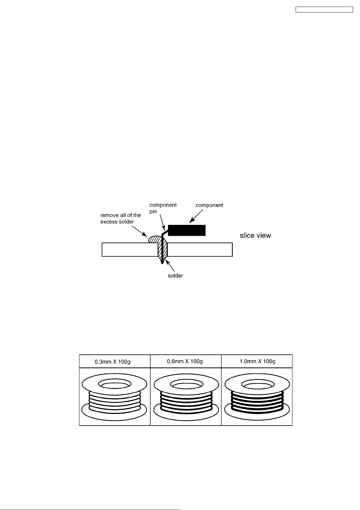
• When applying PbF solder to double layered boards, please check the component side for excess which may flow onto the
• •
opposite side (See figure, below).
1.1. SUGGESTED PbF SOLDER
There are several types of PbF solder available commercially. While this product is manufactured using Tin, Silver, and Copper,
(Sn+Ag+Cu), you can also use Tin and Copper, (Sn+Cu), or Tin, Zinc, and Bismuth, (Sn+Zn+Bi). Please check the
manufacturer’s specific instructions for the melting points of their products and any precautions for using their product with other
materials.
The following lead free (PbF) solder wire sizes are recommended for service of this product: 0.3mm, 0.6mm and 1.0mm.
5
KX-TES824LA / KX-TE M824LA /
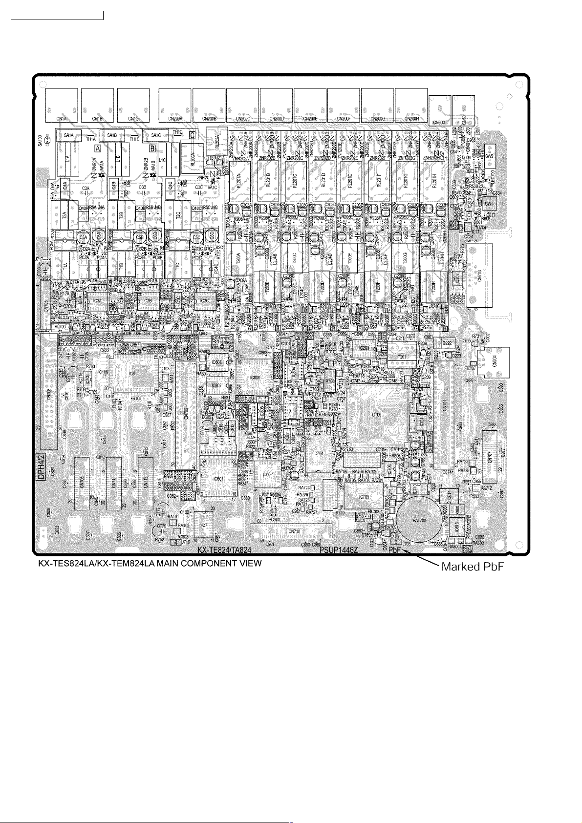
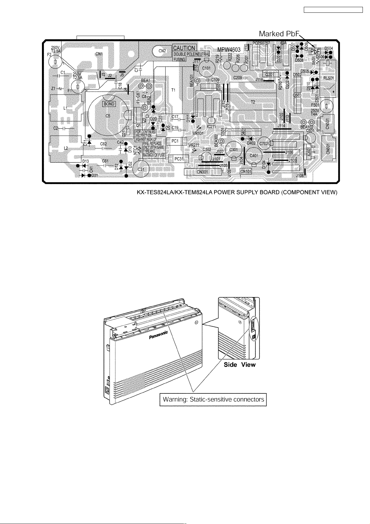
1.2. HOW TO RECOGNIZE THAT Pb FREE SOLDER IS USED
6
KX-TES824LA / KX-TE M824LA /
2 FOR SERVICE TECHNICIANS
ICs and LSIs are vulnerable to static electricity.
When repairing, the following precautions will help prevent recurring malfunctions.
1. Cover the plastic parts boxes with aluminum foil.
2. Ground the soldering irons.
3. Use a conductive mat on the worktable.
4. Do not touch IC or LSI pins with bare fingers.
7
KX-TES824LA / KX-TE M824LA /
3 CAUTION
3.1. SAFETY PRECAUTIONS
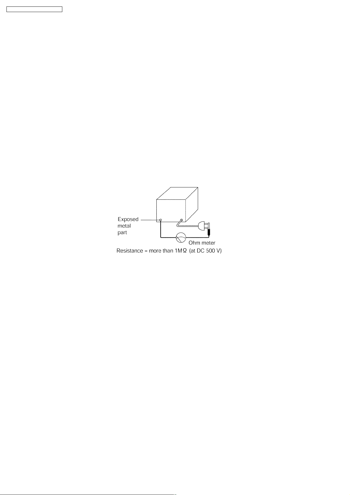
1. Before servicing, unplug the power cord to prevent an electric shock.
2. When replacing parts, use only the manufacturer´s recommended components for safety.
3. Check the condition of the power cord. Replace if wear or damage is evident.
4. After servicing, be sure to restore the lead dress, insulation barriers, insulation papers, shields, etc.
5. Before returning the serviced equipment to the customer, be sure to perform the following insulation resistance test to prevent
the customer from being exposed to shock hazards.
3.2. INSULATION RESISTANCE TEST
1. Unplug the power cord and short the two prongs of the plug with a jumper wire.
2. Turn on the power switch.
3. Measure the resistance value with ohmmeter between the jumpers AC plug and each exposed metal cabinet part, such as
screw threads, control shafts, handle brackets, etc.
Note:
Some exposed parts may be isolated from the chassis by design. These will read infinity.
4. If the measurement is outside the specified limits, there is a possibility of shock hazard. The equipment should be repaired and
rechecked before it is returned to the customer.
3.3. BATTERY CAUTION
1. Danger of explosion if battery is incorrectly replaced. Replace only with the same or equivalent type recommended by the
manufacturer. Dispose of used batteries according to the manufacturer’s Instructions.
2. The lithium battery is a critical component (type No.CR23541). Please observe for the proper polarity and the exact location
when replacing it and soldering the replacement lithium battery in.
3.4. CAUTION
The power socket wall outlet should be located near this equipment and be easily accessible.
8
4 SPECIFICATIONS
4.1. GENERAL DESCRIPTION
Control Bus Original bus (16-bit, 24 MHz)
Switching Space Division CMOS Crosspoint Switch
Power Input 100 V AC to 240 V AC, 1.5A to 0.75A, 50 Hz/60Hz
External Battery +24 V DC (+12 V DC x 2)
Maximum Power Failure Tolerance 300 ms (without using backup batteries)
Memory Backup Duration 7 years
Dialling Outside (CO) Line Pulse (10 pps, 20 pps) or Tone (DTMF)
Extension Pulse (10 pps, 20 pps) or Tone (DTMF)
Intercom Path 4
Mode Conversion Pulse-DTMF
Ring Frequency 20 Hz/25 Hz (selectable)
Operating Environment Temperature 0°Cto40°C
Humidity 10 % to 90 % (non-condensing)
Conference Call Outside (CO) Line 2
Music on Hold (MOH) 1 port
Selectable MOH: Internal/External/Tone
Paging Internal 1
Extension 1 port
Serial Interface Port RS-232C 1
USB 1.1 1
Extension Connection Cable SLT 1 pair wire (T, R)
PT 2-pair wire (T, R, H, L)
DSS Console 1-pair wire (H, L)
Dimension 368 mm (W) x 284 mm (H) x 102 mm (D)
Weight (when fully expanded) Approx. 3.5 kg
KX-TES824LA / KX-TE M824LA /
4.2. CHARACTERISTICS
Terminal Equipment Loop Limit PT 40 Ω
SLT 600 Ω including set
Doorphone 20 Ω
Minimum Leakage Resistance 15000 Ω minimum
Maximum Number of Extension
Instruments per Line
Ring Voltage 75 Vrms at 20 Hz/25 Hz depending on the ringing load
Outside (CO) Line Loop Limit 1600 Ω maximum
Hookswitch Flash/Recall Timing Range 24 ms-2032 ms
Door Opener Current Limit 30 V DC/125 V AC, 3 A maximum
Paging Terminal Impedance 600 Ω
MOH Terminal Impedance 10000 Ω
1 PT or SLT in standard connection
1 PT and 1 SLT in parallel connection
4.3. SYSTEM CAPACITY
4.3.1. System Capacity
KX-TES824 KX-TEM824
Basic System Outside (CO) lines 3 6
Extensions 8 16
Fully Expanded System Outside (CO) lines 8 8
Extensions 24 24
9
KX-TES824LA / KX-TE M824LA /
4.3.2. Maximum Cards Terminal Equipment
ltem KX-TES824 KX-TEM824
Extension Terminal 48 48
3-Port Analogue CO Line and 8-Port Hybrid Extension Card 1 2-Port Analogue CO Line and 8-Port Single Line Telephone Extension Card 1 1
8-Port Single Line Telephone Extension Card 1 1
Message Expansion Card for DISA/UCD OGMs 1 1
4-Port Doorphone Card 1 1
3-Port Caller ID Card 3 3
2-Channel Voice Message Card 1 1
Doorphone 4 4
Door Opener 4 4
Pager 1 1
Music on Hold (MOH) 1 1
DSS Console 2 2
4.3.3. System Data
ltem Max. Quantity
Operator 1
System Speed Dialling 100
One-touch Dialling 24 per extension (PT)
Personal Speed Dialling 10 per extension
Call Park Area 10
Absent Message 6
Toll Restriction (TRS) COS 5
Extension Group 8
Message Waiting 8 per extension
Message for Built-in Voice Message 128 messages (total 60 minutes)
5 SYSTEM OVERVIEW
5.1. SYSTEM COMPONENTS
Model Description
Main Unit KX-TES824LA
KX-TEM824LA
Optional Service Cards KX-TE82461X
KX-TE82474X
KX-TE82480X
KX-TE82483X
KX-TE82491X
KX-TE82492X
KX-TE82493X
Proprietary Equipment KX-T30865
KX-A227X
Advances Hybrid System: 3 to 8 Outside (CO) Lines, 8 to 24 Extensions
Advances Hybrid System: 6 to 8 Outside (CO) Lines, 16 to 24 Extensions
4-Port Doorphone Card
8-Port Single Line Telephone Extension Card
2-Port Analogue CO Line and 8-Port Single Line Telephone Extension Card
3-Port Analogue CO Line and 8-Port Hybrid Extension Card
Message Expansion Card for DISA/UCD OGMs
2-Channel Voice Message Card
3-Port Caller ID Card
Doorphone
Backup Battery Cable
10
5.2. SYSTEM CONNECTION DIAGRAM
KX-TES824LA / KX-TE M824LA /
•
• Connect a display-equipped proprietary telephone (PT) to extension jack 01, as this extension is automatically designated as
• •
the manager extension.
11
KX-TES824LA / KX-TE M824LA /
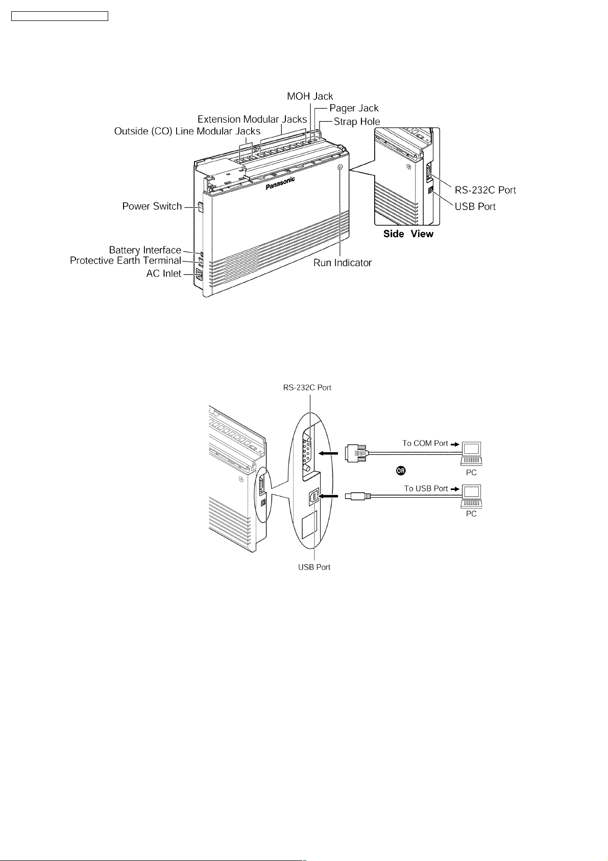
6 NAMES AND LOCATIONS
7 CONNECTION
7.1. SERIAL INTERFACE CONNECTION
12
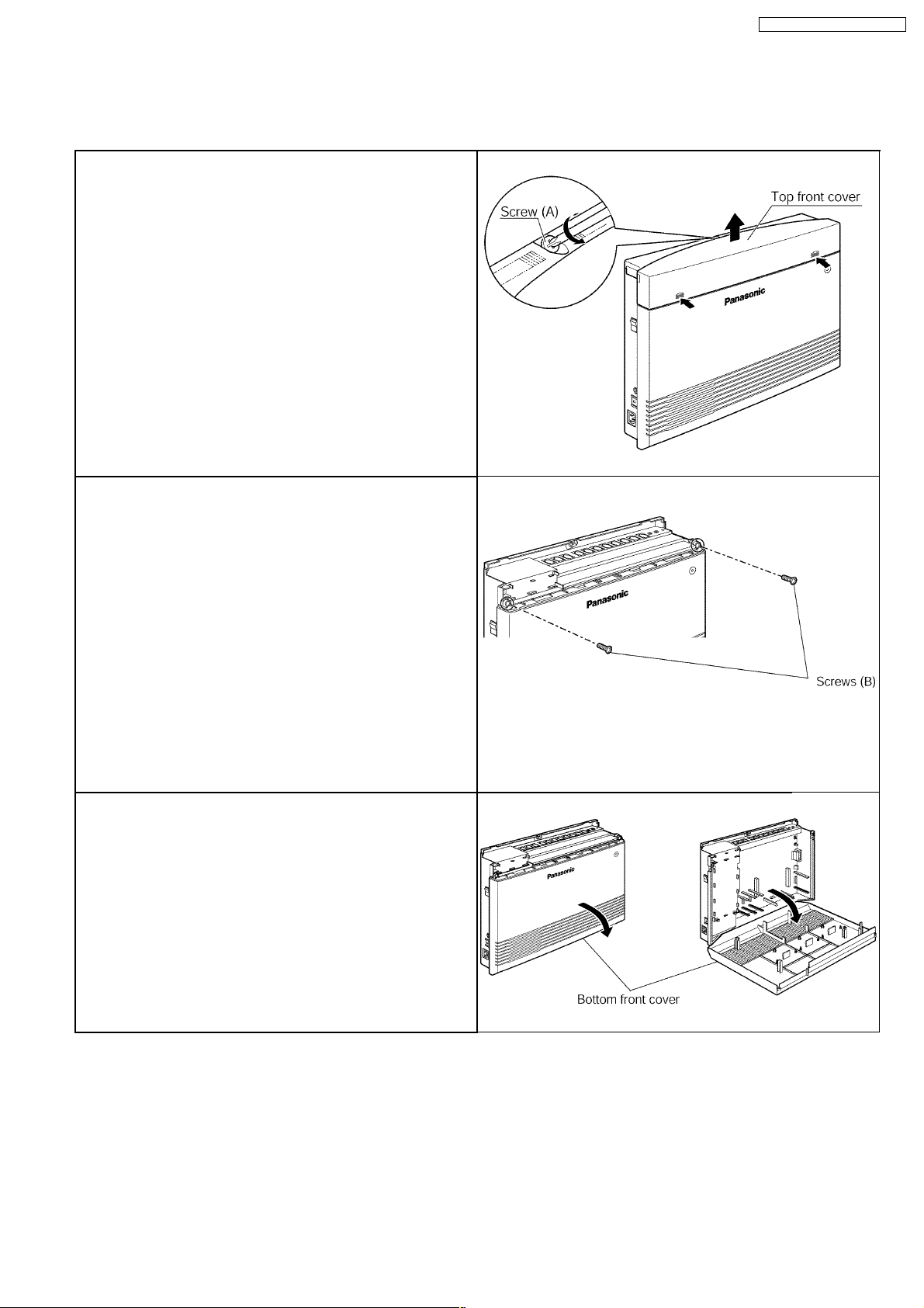
8 DISASSEMBLY INSTRUCTIONS
8.1. DISASSEMBLY INSTRUCTION
1. Loosen the top cover screw (A).
2. Remove the top front cover.
Note
The screw cannot be removed front the cover.
KX-TES824LA / KX-TE M824LA /
3. Remove the 2 bottom-cover screws (B).
4. Open the bottom front cover.
13
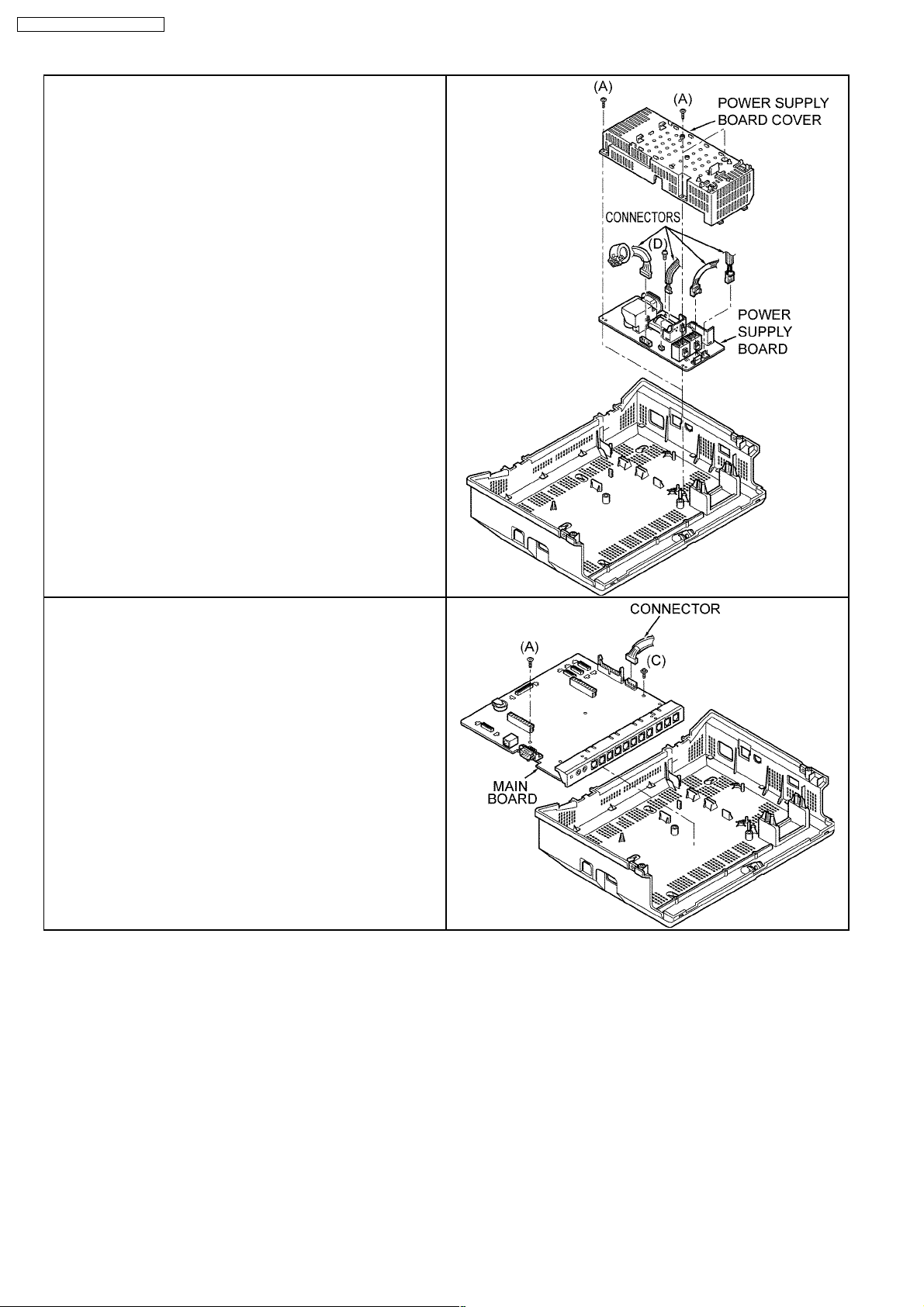
KX-TES824LA / KX-TE M824LA /
5. Remove the 2 screws (A).
6. Remove the power supply board cover.
7. Pull out the 4 connectors.
8. Remove the 1 screw (D).
9. Remove the power supply board.
10. Pull out the 1 connector.
11. Remove the 2 screws (A) and (C).
12. Remove the main board.
14
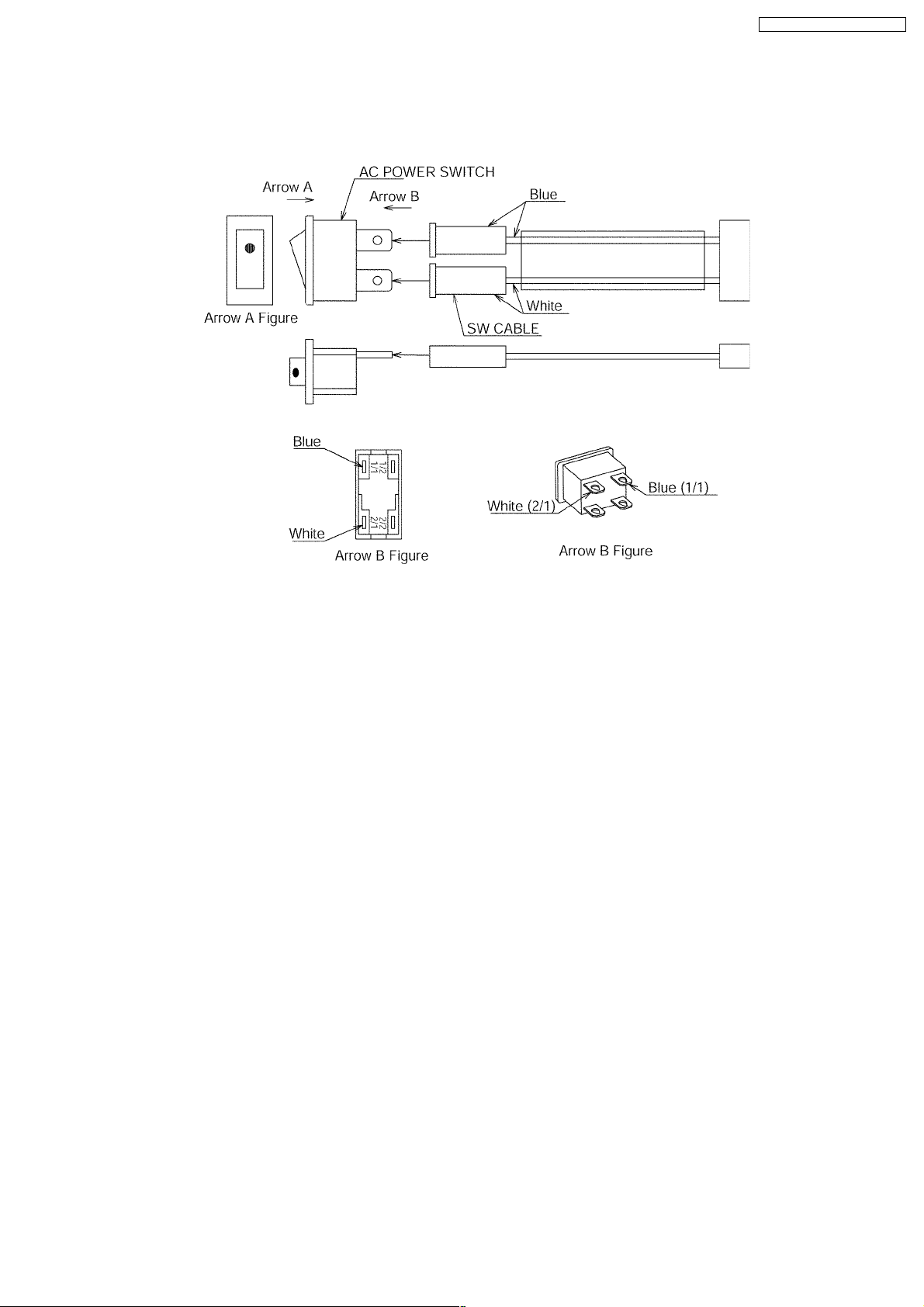
Procedure:
•
• Insert the SW CABLE into AC POWER SWICH.
• •
Caution:
•
• Be sure each colored wire is inserted to the correct lug (very important).
• •
KX-TES824LA / KX-TE M824LA /
15
CID Card #3
0
KX-TES824LA / KX-TE M824LA /
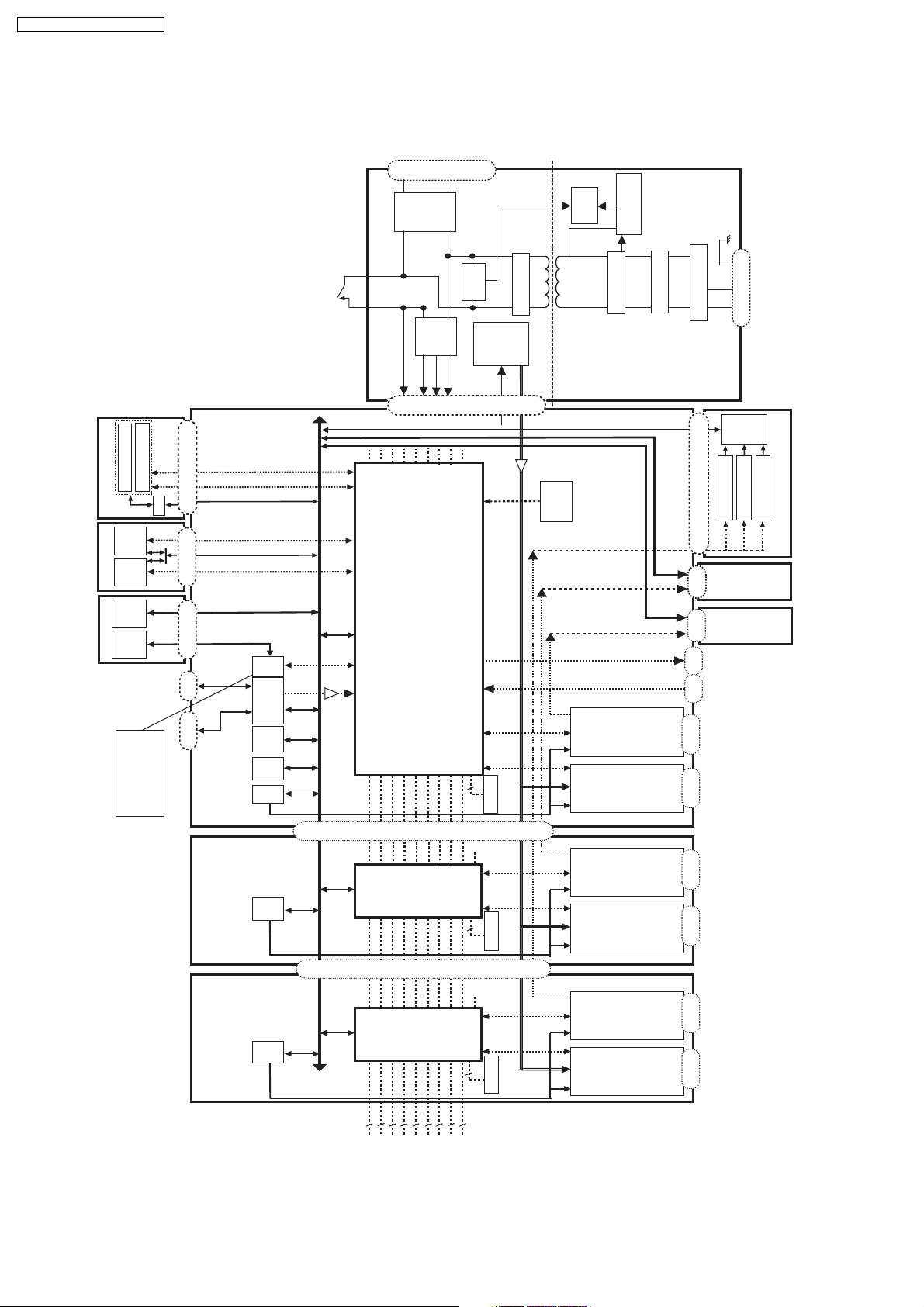
9 BLOCK DIAGRAM
9.1. SYSTEM BLOCK DIAGRAM
Power Switch
DPH Block #1,#2
DPH4 Card
BV Card
IC3 IC4
SRAM
IC1 IC2
OGM Card
Serial
Int. CID x 3
CN708
DPH Block #3, #4
PIO
DSP#2
CN707
DSP#1
8Mbit
CN710
Flash
USB
CN704
RS232C
CN703
BGM
MODEM(Rx, Tx)
OGM(Play, Rec) x2
1AP Card
2AP Card
DOOR2
DOOR1
IC700
IC704
IC705
IC6
IC10
BV2
BV1
CPU DSP
SRAM
Flash
PIO
PIO
To ne
ROM
E
Host I/F
E
x
x
pan
pan
s
s
V
G
24
battery
backup
change
Voltage
-15 V
+15V
+27V
705
C
N
Cross Point
i
o
nConn
IC500
Cross Point
i
o
nConn
N
D
circuit
check
Volt age
Amp.
Ringer
+3.3V
25Hz
IC600, IC601, IC602
CO1-3
ext1-8
2
DTMF-R
t
c
e
CO4-6
IC502
ext9-16
IC501
2
DTMF-R
t
c
e
circuit
Bell
IC613
IC614
o
IC511
IC512
o
Rectification
r
r
AC75V
IC601
25Hz
DTMF-G
control
IC7
for CO
3port
8port
3port
8port
circuit
Detect circuit
Over current
Rectification
POWER
Ext Paging
Ext Music
Co
Block
Block
Extension
Co
Block
Block
Extension
L1, L2
noise filter
SUPPLY
Z1
Surge protector
CN712
CN711
CN706
CN601
CN60
PIO
FPGA
FSK Detect x3
IC7
IC1A~C
#2
CID
Card
#1
CID
Card
FG
N
L
AC IN
S/P
IC8
DTMF Detect
Stutter Detect x3
IC2A~C
#3
CID
Card
Same as
#3
CID
Card
Same as
3AP Card
IC700
CO7-8
IC701
PIO
Cross Point
4
2
1
2
Tone
Int.CID
Paiging
IC702
3BV2
1
2
INT
DPH
BGM
DTMF-G
IC703
8
CO
2
ext17-24
DTMF-R
IC704
IC705
Co
2port
Block
8port
Block
Extension
Jack x2 Jack x8 Jack x3 Jack x8 Jack x3
Jack x8
KX-TES824LA/KX-TEM824LA SYSTEM BLOCK DIAGRAM
16
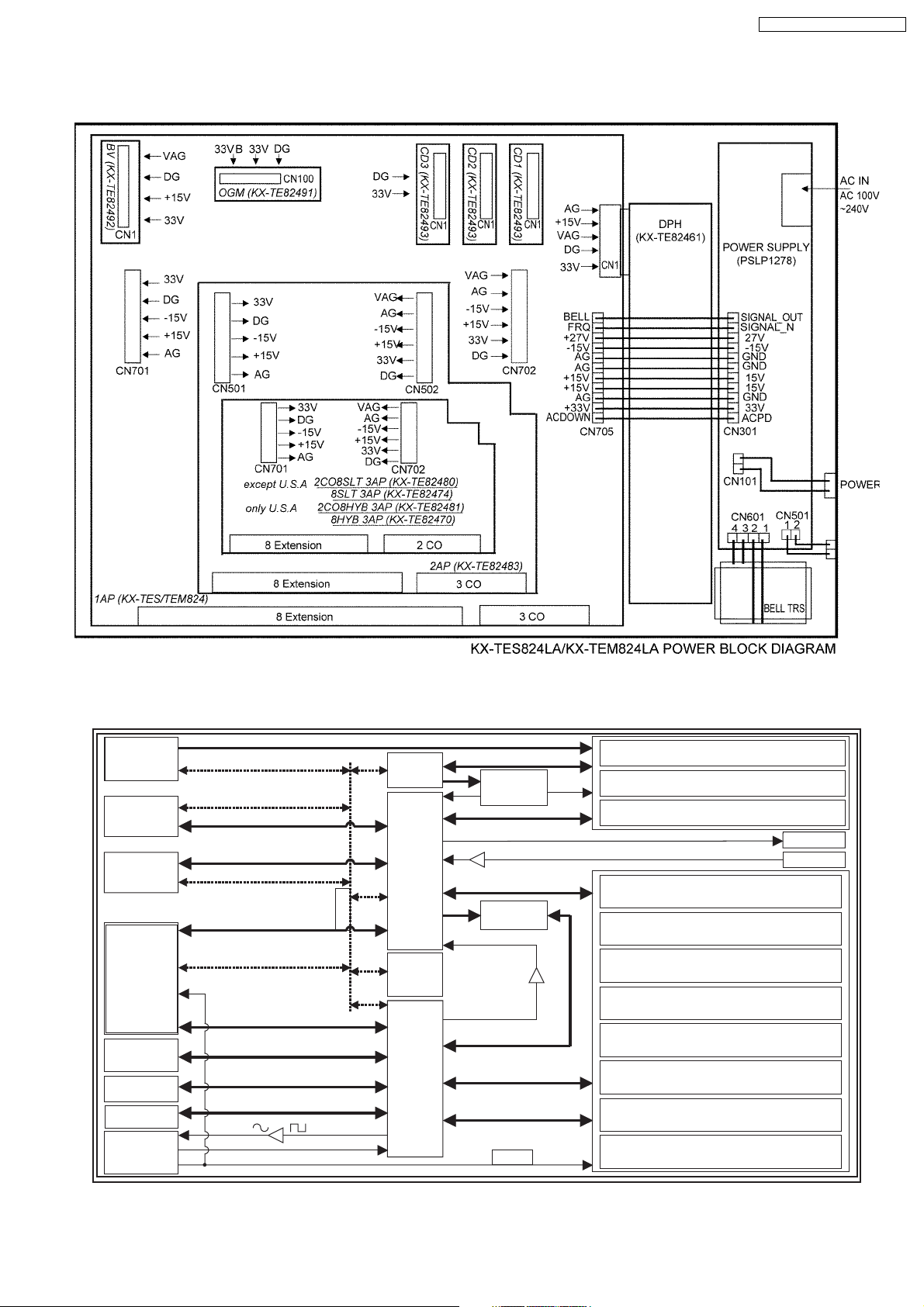
9.2. POWER BLOCK DIAGRAM
KX-TES824LA / KX-TE M824LA /
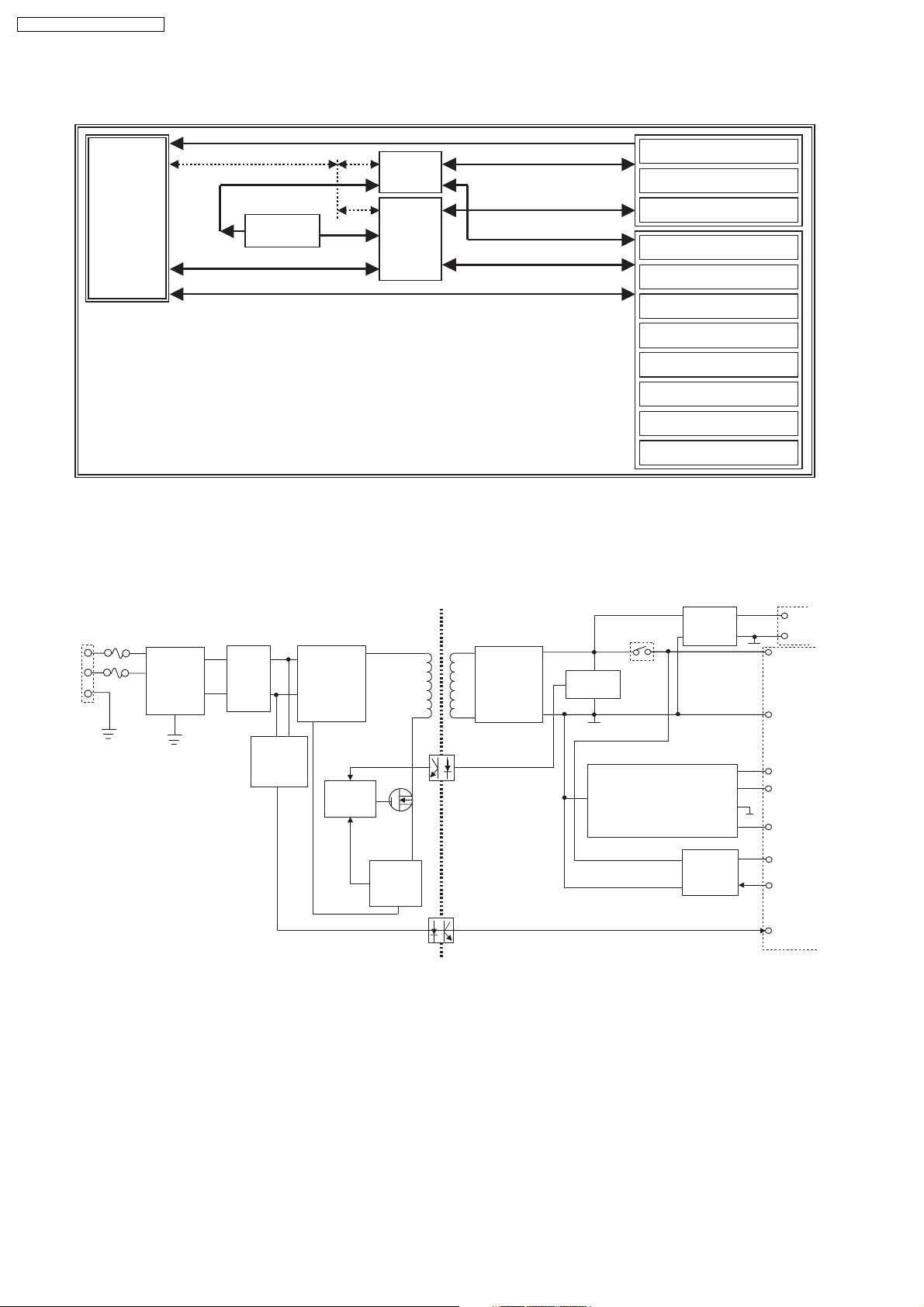
9.3. KX-TES824LA/KX-TEM824LA 1AP BLOCK DIAGRAM
CONNECTOR
Door Phone
Door Opener
CONNECTOR
CONNECTOR
CN701, CN702
CONNECTOR
CONNECTOR
POWER UNIT
CONNECTOR
CO CID
CN706
CN708
BV Card
CN707
Exp308
(2AP)
/Exp208
(3AP)
Card
EXP
CN710
OGM Card
CN703
D-Sub
CN704
USB
CN705
(APT i/f)PRX2-3, PTX2-3, PTXE1-3
25Hz
DOOR1, 2
TAM1-2, TONE
CO4-8
(DSP)Serial Flash i/f
(UART)RXD, TXD
TONE(D)
NINT AC
Host i/f
IC6
PIO
ASIC
CROSS
POINT
IC600
IC601
IC602
IC709
ROM
IC704
SRAM
ASIC
8086
DSP
PIO
APT i/f
IC700
DTMFR(1,2)
IC613, IC614
620,440,350Hz
TONE
Q1-4,TOE1,2,STD1,2
(I/O)HOOK1-8,BELL1-8
(APT i/f)PRX,PTX,PTXE1-3
IC7
DTMF
Generator
CO1-3
PAGE
BGM
EXT1-8
(For EXT)
BELL
(I/O)
CO1
CO2
CO3
EXT1
EXT2
EXT3
EXT4
EXT5
EXT6
EXT7
EXT8
CN601
CN600
Paging jack
MOH jack
KX-TES824LA/KX-TEM824LA 1AP BLOCK DIAGRAM
17
KX-TES824LA / KX-TE M824LA /
9.4. KX-TEM824LA 2AP BLOCK DIAGRAM
Exp308
(2AP)
/Exp208
(3AP)
Card
EXP
CONNECTOR
CN501, CN502
Host i/f
Q1- 4,TOE1,2,STD1,2
IC510, IC511
DTMFR(1,2)
(For EXT)
CO4-6
(APT i/f)PRX2,PTX2,PTXE1-3
CID4-6
PIO
ASIC
IC10
CROSS
POINT
IC500, IC501, IC502
(I/O)
CO4-6
(I/O)HOOK9-16,BELL9-16
EXT9-16
CO4
CO5
CO6
EXT9
EXT10
EXT11
EXT12
EXT13
EXT14
EXT15
EXT16
KX-TEM824LA 2AP BLOCK DIAGRAM
9.5. KX-TES824LA/KX-TEM824LA POWER SUPPLY UNIT BLOCK DIAGRAM
Q503
RL501
+27V
GND
+24V
GND
AC IN
L
N
CN1
Q503
RL501
D10~D13, C5
F1
Surge
F2
Absorber
Z1
Noise
Filter
L1, L2
Primary Circuit
Rectification
&
Smoothing
T1
D101, C101
Secondary Circuit
Rectification
&
Smoothing
Voltage
Detection
SW
Q101
Battery
Back up
FG
D31
D32
AC Input
Detection
(14)
Power
Down
Q22
Q23
Controller
Q1
Q2
Over
Current
Detection
PC1
PC31
Q201, T2, IC201
DC-DC
Converter
IC601
Ringer
Amplifier
KX-TES824LA/KX-TEM824LA POWER SUPPLY UNIT BLOCK DIAGRAM
+15V
3.3V
-15V
OUTPUT
AC75V 25Hz
INTPUT
20/25Hz
AC
Alarm
CN301
18

KX-TES824LA / KX-TE M824LA /
10 EXPLANATION OF BLOCK DIAGRAM
10.1. MAIN UNIT (KX-TES824LA/KX-TEM824LA)
10.1.1. Power Supply Circuit
This power supply unit is a switching power supply. Power supply unit supplies DC voltage (+27V,+15V,-15V,3.3V) to main board
and other optional cards. And this unit has an adaptor circuit to back up battery. And this unit amplified the BELL signal (20/25Hz
sign wave outputted from the ASIC) and supply bell signal to the telephone.
10.1.2. COL Interface Circuit
There are the interface circuits linking the CO line (CO1 -CO3) and the cross point circuit section.
In case of KX-TEM824, the system has 6CO line (CO1 - CO6).
10.1.3. Cross Point Circuit
This is a space division switching system for connecting the following:
The eight extension circuits with the eight CO, DTMF generator, DTMF receiver, INT-CALL ID, MODEM, OGM, VB, paging, music
on hold, tone etc.
It is composed of 3 C-MOS IC´s. (8 X 16 matrix: 2pcs and 4 X 8 matrix: 1pce).
*In case of KXTEM824, the system has 6 C-MOS IC´s (8 X 16 matrix: 3pcs and 4 X 8 matrix: 2pce, 8 X 8 matrix: 2pce).
10.1.4. Intercom Circuit
This is the interface circuit of the single line telephone, and it is composed of 8 intercom circuit (ICM1-8) In case of KX-TEM824,
the system has 16 intercom circuits(ICM1-16).
10.1.5. Power Failure Through Call Switching Circuit
KXTES824 have one power failure transfer circuit (CO1-EXT101).
In case of KXTEM824,the system has 2 power failure circuit (CO1-EXT101 CO4 -EXT109).
10.1.6. Data Communication Circuit
The APT i/f module which performs communication with a private telephone machine is built in ASIC.
8ch are controlled per block. Control of 3 blocks (24ch) is possible for ASIC at the maximum.
10.1.7. Control Circuit
A control block consists of only the [ASIC] CPU (compatibility with Intel 8086) (IC700), Flash ROM (8Mbit) (IC705), SRAM (4Mbit)
(IC704), and PIO ASIC (IC6). PIO ASIC mainly performs extension control and PIO built in ASIC CPU mainly performs extension
control. RTC (Real Time Clock) and SRAM inside CPU are backed up by the lithium battery in order to hold time, system data, etc.
10.1.8. Tone Generator Circuit
The rectangle wave generated by the timer of ASIC is changed into sine wave with a low path filter, and various tones are
generated.
10.1.9. DTMF Generator Circuit
A DTMF generator is used for dispatch to outside line, and communication with the voice mail connected to the extension.
10.1.10. DTMF Receiver Circuit
The circuit which receives the Dial Tone Multi Frequency by which extension dispatch is carried out with the DTMF receiver
connected to the crossing point.
10.1.11. Int Call ID Circuit
FSK/Dial Tone Multi Frequency generated by DSP in ASIC are connected even to a crossing point through AMP. The circuit which
sends out a CALLID signal to the telephone connected to an extension by connecting the line of INT-CALL-ID with arbitrary
extensions.
10.1.12. Modem Circuit
The MODEM signal generated by DSP in ASIC is connected even to a crossing point through AMP.
The circuit which connects the line of MODEM with arbitrary outside line, and enables MODEM communication with outside line.
19

KX-TES824LA / KX-TE M824LA /
10.1.13. USB Circuit
The circuit which makes communication possible by PC and 1.1 standards by the USB controller in ASIC.
10.1.14. OGM Circuit
4M connected to ASIC by the memory controller in ASIC A maximum of 3-minute storing of OGM is possible to a serial flash Circuit.
10.1.15. Ring Signal Generator Circuit
This section generates the ring signal for the single line telephone. A 20/25Hz square wave is generated by the ASIC timer and sent
to low pass filter and the ringing signal amplifier circuit and stepped by BELL transformer, and then passed it through the ringing
signal switching relay to the single line telephone.
10.1.16. SMDR Interface Circuit
This is the RS232C interface port. When the port is connected to a printer. The port can be used to output the SMDR feature
recording messages and the contents of the system program.
10.1.17. Door Phone Interface
An intercom card interface consists of two intercom paths connected to a crossing point, and address data and CS signals.
10.1.18. OGM Interface
An OGM card interface consists of the memory control signal, and the address data and CS signal which are connected to ASIC.
10.1.19. Call ID Interface
A CALLID card interface consists of three CALLID signal lines from outside line, and address data and CS signal.
10.1.20. BV Interface
BV card interface consists of two BV telephone call paths connected to a crossing point, and address data and CS signals.
20
11 CIRCUIT OPERATION
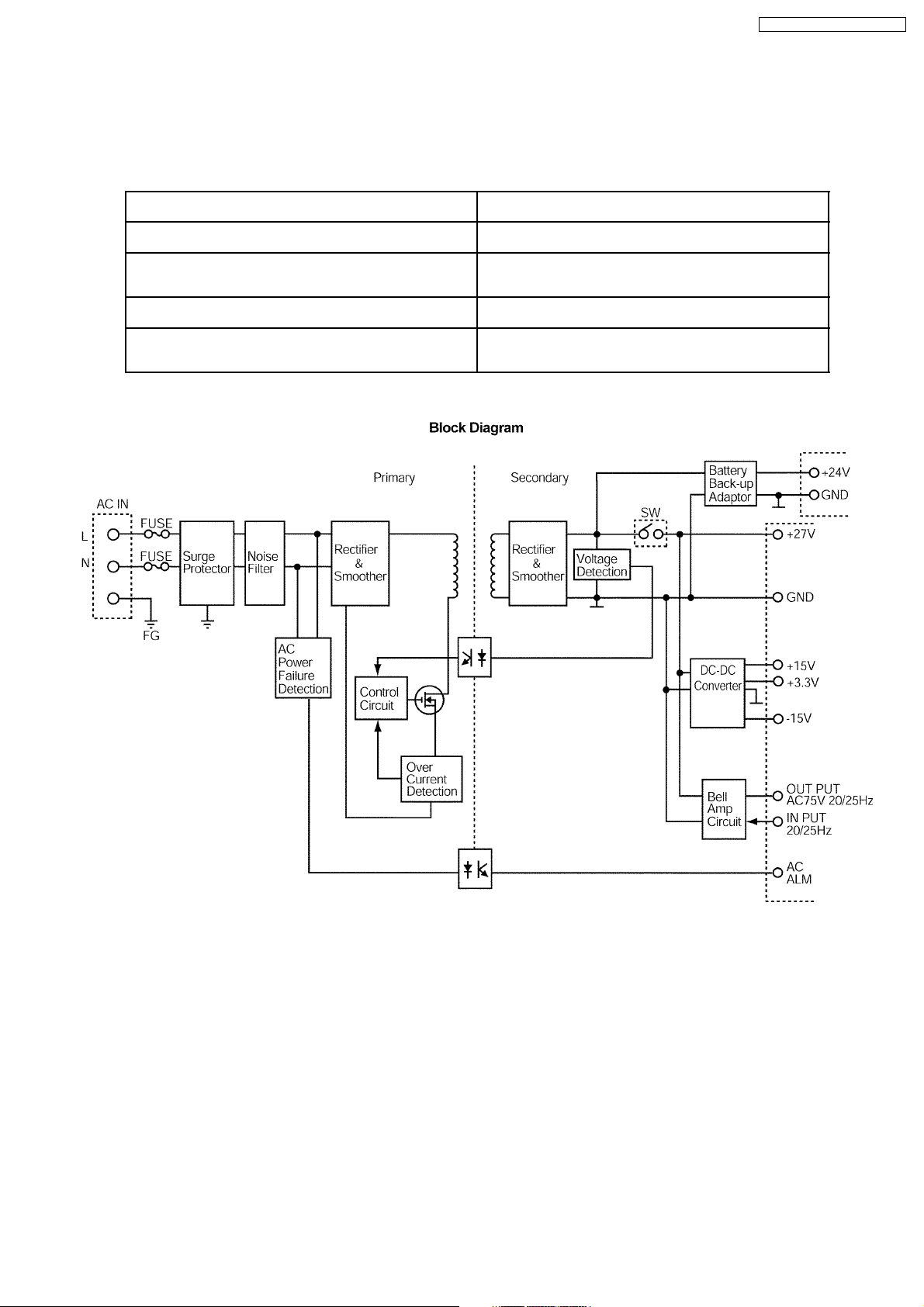
11.1. POWER SUPPY CIRCUIT
11.1.1. The function of the power unit are listed below
KX-TES824LA / KX-TE M824LA /
AC-DC Inverter Function This function isolates and transduces the AC input voltage to
DC-DC Converter Function This function outputs DC+15V, -15V and 3.3V from the
Ringing Signal Output Function Based on the 20/25Hz sine wave signal output from KX-
AC Power Failure Detection This function detects any cut off of the AC power supply and
Battery Back Up Adaptor Function This function connects battery and service unit without battery
DC input and output of DC27V.
inputted DC27V.
TES824/KX-TEM824, this function generates ringing and
supplies to the system.
outputs an AC alarm signal to the CPU.
adaptor, only needs a cable connected to the battery and
service unit.
21

KX-TES824LA / KX-TE M824LA /
11.1.2. Control Section
1) AC-DC Inverter Function
The AC input voltage is rectified and smoothed by D10-13 and C5. The obtained DC voltage is converted into a rectangular wave
by the switching transistor Q1, then isolated and transduced by T1. This converted rectangular wave is rectified and smoothed by
D101 and C101 to output DC27V. The DC27V is transmitted to the primary side by PC1 and then PWM- controlled to keep
constant. The switching frequency of Q1 is approximately 100KHz (70KHz~160KHz).
2) DC-DC Inverter Function
The DC27V as input is converted into a rectangular wave by the switching transistor Q201, then isolated and transduced by T2.
DC+15V, -15V and 3.3V are outputted by a rectification smoothing circuit composed of D401, D301, D701, C401, C301 and C702.
The +3.3V of the three outputs is PWM-controlled by IC201 to keep constant.The switching frequency of the Q2 is approx. 55 KHz.
3) Ringing signal output function
Ringing signal (20/25Hz, 75Vac from main board) is amplified in power by power amplifier circuits (including of IC501, R601~R608,
C601~C603).
Ringing signal amplified in power is transmitted to the ringing transformer through pin 4 of CN601.
4) AC Power Failure Detection
AC power failure is detected by D31~D32, R33~R41, C31, PC31.
When AC power is on, PC31 is on.
When AC power is turned off, PC31 is off.
5) Battery back up function
This back up battery adaptor circuit has DC supply function, from battery (+24V) to service unit and DC charge from service unit
to battery (+24V). Charge current is typ. 0.4A.
22
KX-TES824LA / KX-TE M824LA /
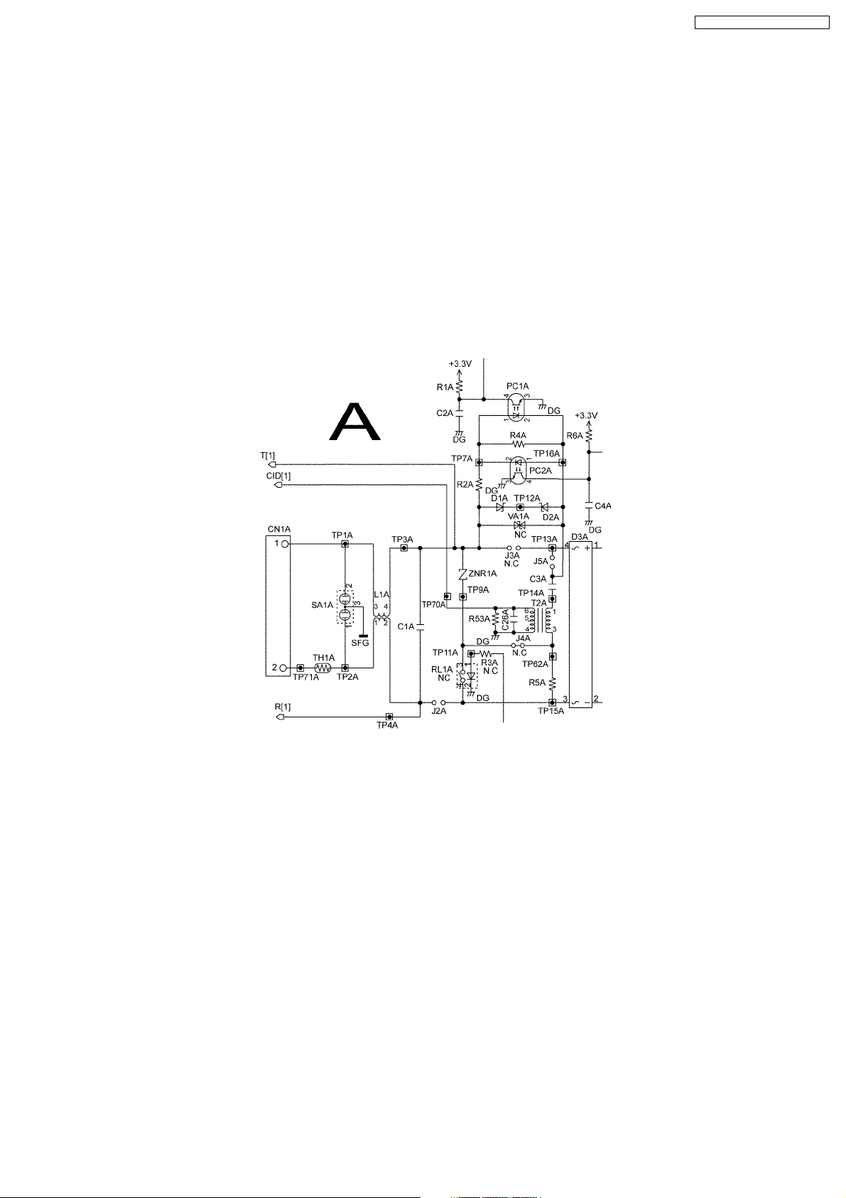
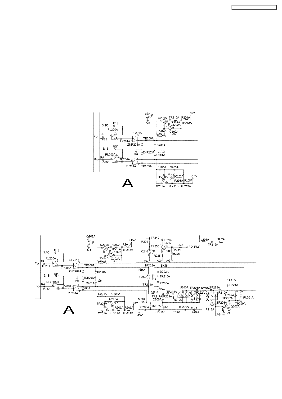
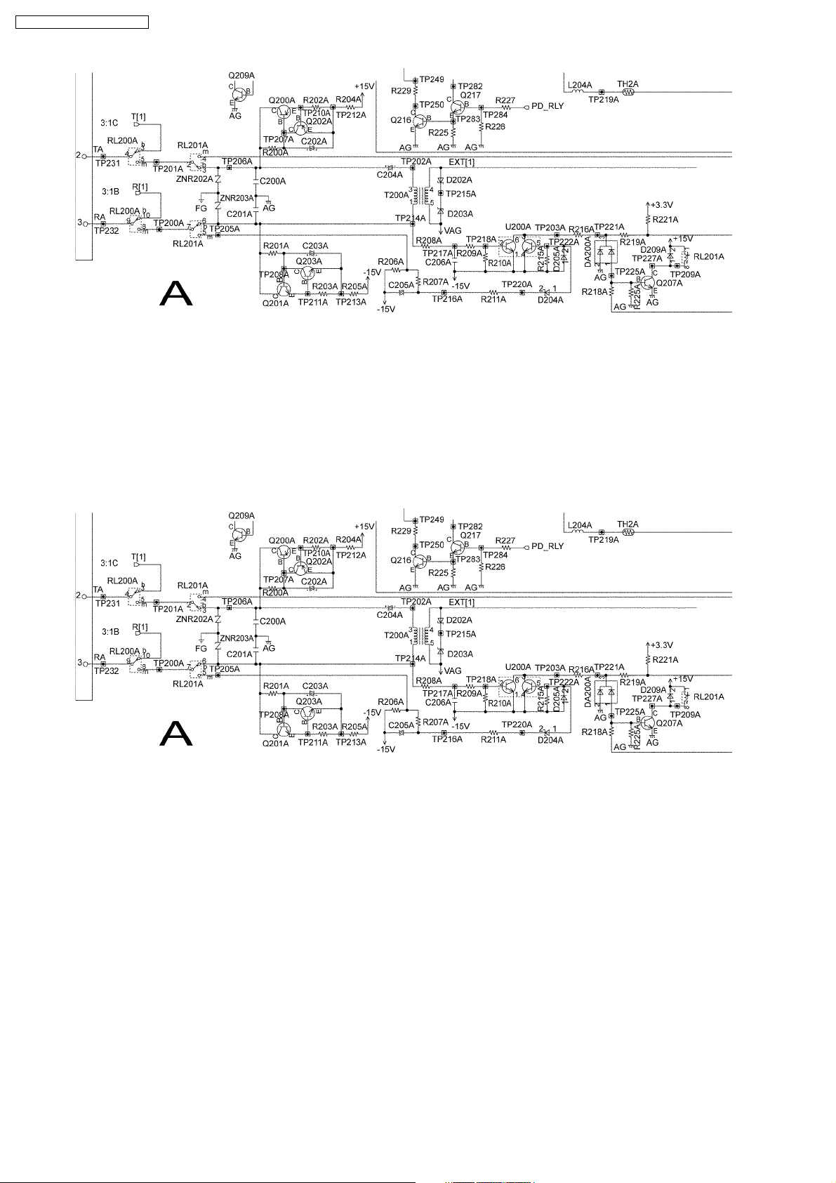
11.2. CO INTERFACE CIRCUIT
11.2.1. Composition
This is composed of the following circuit:
1) Bell signal detection
2) DC loop formation circuit
3) Pulse dial transmission circuit
4) CALL ID interface circuit
5) COL bidirectional amplifier circuit
1) Bell signal detection
When CO line is idle, photo coupler PC1, PC2 are OFF.
When there is an incoming signal from CO line, the current flows PC1 as in the following way.
Tip → L1 → R2 → PC1(1-2) → C3 → T2 → R5 → L1 → Ring: This cause pin4 of PC1 to change the level from High to low.
Ring → L1 → R5 → T2 → C3 → PC2(1-2) → R2 → L1 → Tip: This cause pin4 of PC2 to change the level from High to low.
23
KX-TES824LA / KX-TE M824LA /
2) DC loop formation circuit
In the off hook status, PC5 is ON.
DC loop path:
Tip→L1→D1→D2→D3→Q10(E-C)→Q1(C-E)→R9→R8→D3→L1→Ring
At this time, the output of the photo coupler PC1 changes level from High to low.
Ring→L1→D3→R8→R9→Q1(E-C)→Q10(C-E)→D3→D2→D1→L1→Tip
At this time, the output of the photo coupler PC2 changes level from High to low.
Afterwards, G/A monitor this change (low level to high level). If the high level continues for a specified time set by system data
programming. G/A assumes that CO line has become On hook status. And the CO line circuits is restored to the idle status.
3) Pulse dial transmission circuit
When the Off hook status, pulse dial transmission is executed by alternating On hook and Off hook. The status of On hook or
Off hook is controlled by the switching transistor Q10.
24
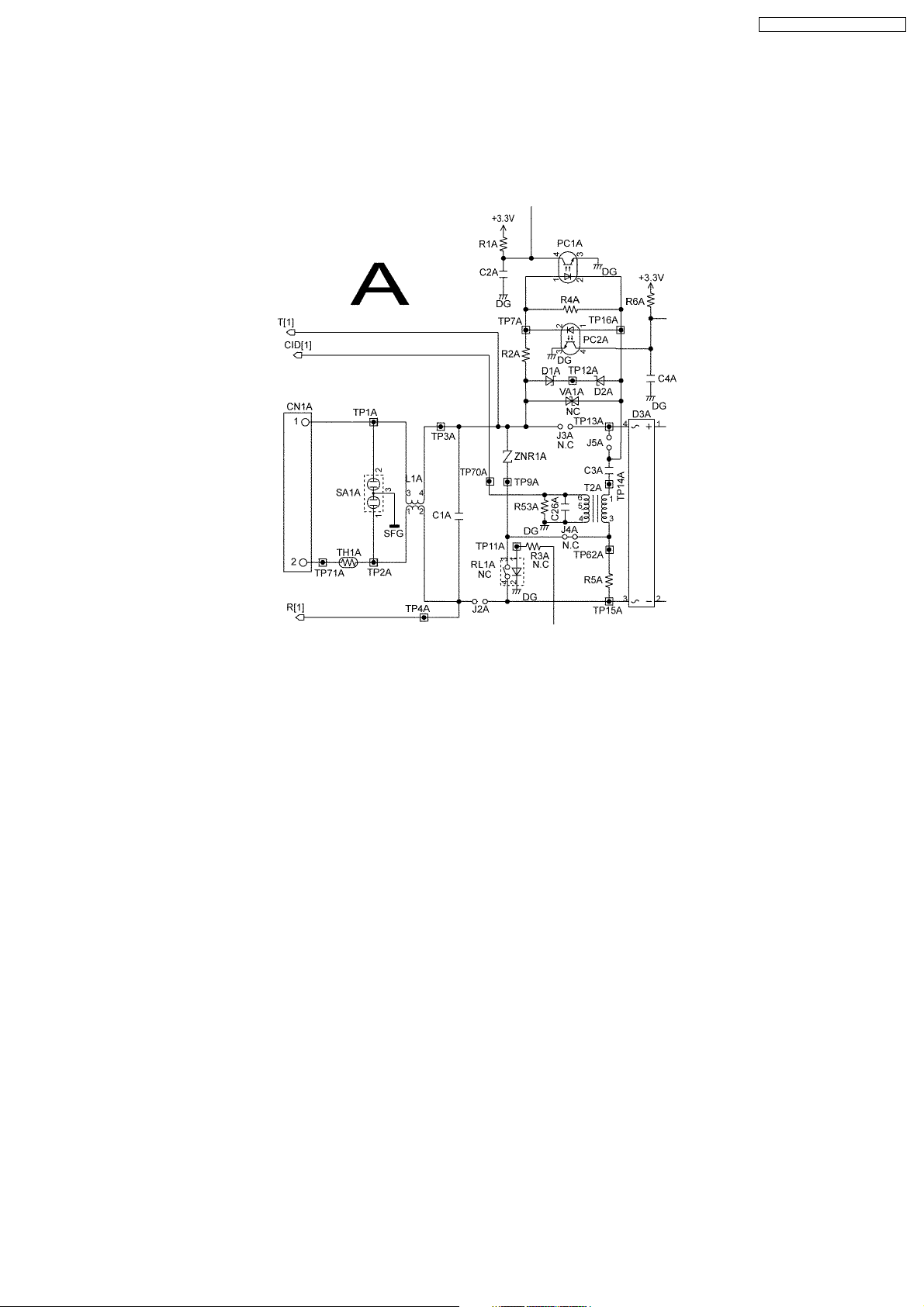
KX-TES824LA / KX-TE M824LA /
4) CALL ID interface circuit
It is insulated by the transformer in a COL circuit, and the call ID signal inputted from outside line is transmitted to a CALLID
option card.
The flow of a CALLID signal
Tip→L1→R2→PC1(1-2)→C3→T2→R5→L1→Ring
Ring→L1→R5→T2→C3→PC2(1-2)→R2→L1→Tip
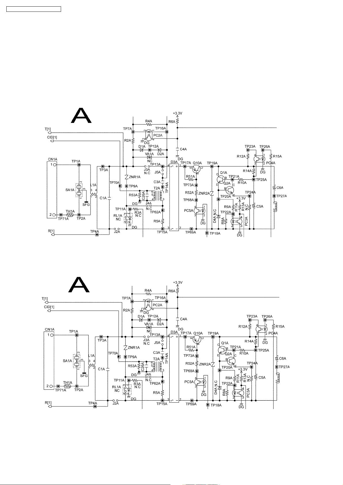
5) COL Bidirectional Amplifier circuit
This circuit consists of bidirectional amplifier function for communication between the extensions and COL, returns loss
compensation for conference, shunt function and mute function.
(Composition)
For transmitting signals from the extensions to COL, this circuit consists of R34, R35, R26, R27, R18, R29, C14, C15, C10, C16
and the operational amplifier (IC1).
For transmitting signals from the COL to extensions, this circuit consists of R24, R25, R31, R28, R37, R30, C12, C13, C17, C18,
and the operational amplifier (IC1).
COL side-tone suppression circuit which includes a balanced network BN1 consists of R22 R23, C11 and R16, R17, R20, R21.
EXT side-tone suppression circuit which includes a balanced network BN2 consists of R41, R42 and R40, R43, R38, R39.
Also extension side-tone suppression circuit which includes a balanced network BN3 consists of R45, R46 for supplementing
side-tone suppression during the conference communication.
The analog switch (IC2) is used for the following:
(1) Conference (Pin 6, 8 and 9)
(2) Shunt (Pin 12, 10 and 11)
(3) Mute (Pin 13, 1 and 2)
25
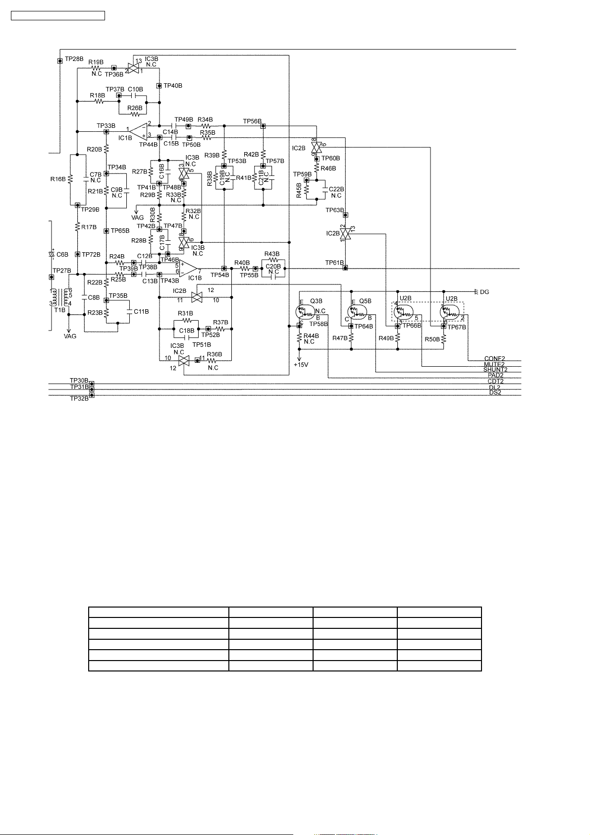
KX-TES824LA / KX-TE M824LA /
1) Conference switch
Normally, pin 6 of the analog switch IC2 is low level, but during conferences, this pin becomes high level. Because, during
conferences, it should compensate the return loss by connecting the balance network BN2 and the balance network BN3 in
parallel.
2) Mute switch
The mute switch consists of pin 13, 1 and 2 of the analog switch(IC2). This switch has the following functions.
a) When a dial signal (DP) is sent to the COL, signals from the extensions are blocked.
b) When the hold on music is sent to the COL, signals from the extensions are blocked.
c) When the COL interface circuit is in the idle state, oscillation of COL bidirectional amplifier is inhibited. When pin 13 of IC2
changes to low level, the interval between pins 1 and 2 of the analog switch turns off, and signals are blocked.
3) Shunt switch
The shunt switch consists of pin 12, 10 and 11 of analog switch IC2.It is used to prevent the pulse dialing signal which is
transmitted to the extensions. When pin 12 of IC2 changes to high from low, the analog switch becomes ON (the interval
between pin 10 and 11), and GAIN of the COL cross point operational amplifier becomes zero.
Shunt SW Mute SW Conference SW
pin no. of analog switch 12 13 6
No connection (idle) H (on) L (off) L (off)
Two party call L (off) H (on) L (off)
Conference L (off) H (on) H (on)
Hold on music transmission L (off) H (on) L (off)
Condition of COL interface amplifier circuit and analog switches.
26
KX-TES824LA / KX-TE M824LA /
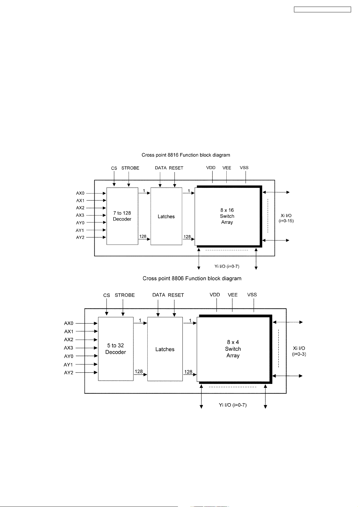
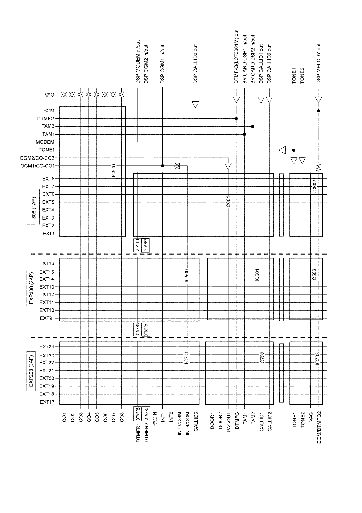
11.3. CROSS POINT SWITCH CIRCUIT
11.3.1. Composition
The cross point circuit composed of three cross point switch IC´s (IC600 and 601:8X16, IC602:4X8).
*In case of KX-TEM824, the system add more cross point switch IC´s (IC500:8X16, IC501:8X8, IC502:4X8) which are in KX-
TE82483.
1) Cross Point Switch IC Operation
The cross point SW (IC600, IC601) contains a 8X16 array of cross point switches along with a 7 to 128 line decoder and latch
circuits. Any one of the 128 switches can be addressed by selecting appropriate seven address bits. The selected switch can
be turned on or off by applying either logical one or zero to the DATA input. Chip select allows the cross point array to be
cascaded for matrix expansion. Start a new line at this point SW´s (IC602) contain 4X8 array of cross point switches along with
a 5 to 32 line decoder and latch circuits.
Any one of the 32 switches can be addressed by selecting appropriate five address bits. The selected switch can be turned on
or off by applying either logical one or zero to the DATE input. Chip select allows the cross point array to be cascaded for matrix
expansion.
27
KX-TES824LA / KX-TE M824LA /
28
KX-TES824LA / KX-TE M824LA /
11.4. INTERCOM CIRCUIT
11.4.1. INTERCOM CIRCUIT
1) Composition
This is composed of the following circuits:
a) +15V power source for the extension telephones
b) Hook detect for SLT and pulse dialing detect
c) Bell ring trip section
2) Circuit operation
a) Power supply to the telephone
With the telephone off hook, a DC loop is formed, and current is supplied to the telephone. This circuit is limited to about 30mA
by Q200, Q202, R202, R204 and Q201, Q203, R203, R205.
+15V→R204→R202→Q200→RL201→telephone→RL201→Q201→R203→R205→-15V
b) Hook detect for SLT and pulse dialing detect
When the telephone handset is taken off, DC loop is formed and the collector of U200 3,6 pin change to L from H.
The ASIC detects the off hook condition.
When the handset is replaced back on hook, the DC loop is interrupted and collector of U200 3,6 pin change to H from L and
EXT Pulse dialing is input either in the on hook or off hook condition, and the break number (on hook condition) is counted and
read as the dial number.
c) Bell ringing trip section
When the telephone is a signal line telephone, extension calling is executed by means of a ringing signal. When the ringing
signal is supplied, RL201 turns ON and the current flows are as follows:
Bell transformer → ringing signal line → RL201 → telephone → R206 → -15V → Bell transformer
29
KX-TES824LA / KX-TE M824LA /
11.5. POWER FAILURE THROUGH CALL SWITCHING CIRCUIT
11.5.1. Circuit operation
If an AC power failure lasts longer than one second (momentary power failure), the COL is directly connected to the extension.
The COL1 will be connected with EXT101.
When power failure, RL200 switches from EXT-line to CO [T/R].
*In case of KX-TEM824, and the COL4 will be connected with EXT109.
*In case of KX-TE82480, and the CO7 will be connected with EXT117.
30
 Loading...