Panasonic KX-TCD150FXB, KX-TCD150FXC, KX-TCD152FXB, KX-TCA115EXB, KX-TCA115EXC Service Manual
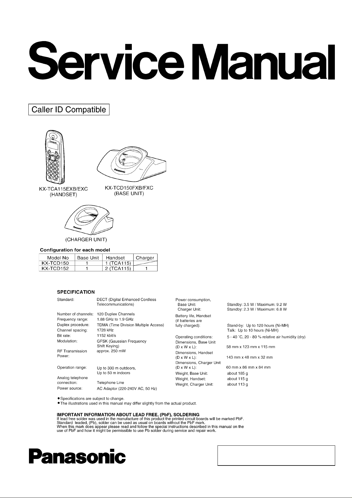
ORDER NO. KM40507819CE
Telephone Equipment
KX-TCD150FXB
KX-TCD150FXC
KX-TCD152FXB
KX-TCA115EXB
KX-TCA115EXC
Digital Cordless Phone
Black Version
Dark Blue Version
(for Central Europe)
© 2005 Panasonic Communications Co., Ltd. All
rights reserved. Unauthorized copying and
distribution is a violation of law.
KX-TCD150FXB / KX-TCD150FXC / KX-TCD152FXB / KX-TCA115EXB / KX-TCA115EXC
Note:
Because CONTENTS 4 is the extract from the Operating Instructions of this model, it is subject to change without notice. You can
download and refer to the original Operating Instructions on TSN Server for further information.
CONTENTS
Page Page
1 ABOUT LEAD FREE SOLDER (PbF: Pb free) 4
1.1. Suggested PbF Solder
1.2. How to recognize that Pb Free solder is used
2 FOR SERVICE TECHNICIANS
3 CAUTION
4 OPERATING INSTRUCTIONS
4.1. BATTERY
4.2. LOCATION OF CONTROLS
4.3. Connection
4.4. Guide to Settings
4.5. For Service Hint
5 DISASSEMBLY INSTRUCTIONS
5.1. Base Unit
5.2. Handset
5.3. Charger Unit
6 ASSEMBLY INSTRUCTIONS
6.1. Warning When Constructing the Base Unit
6.2. How to Replace the Handset LCD
7 TROUBLESHOOTING GUIDE
7.1. Check Power
7.2. Check Battery Charge
7.3. Check Link
7.4. Check Handset Transmission
7.5. Check Handset Reception
7.6. Check Caller ID
7.7. Bell Reception
8 TROUBLESHOOTING BY SYMPTOM (BASE UNIT AND
CHARGER UNIT)
8.1. Check Point (Base Unit)
8.2. The Setting Method of JIG (Base Unit)
8.3. Adjustment Standard (Base Unit)
8.4. Check Point (Charger Unit)
8.5. Adjustment Standard (Charger Unit)
9 TROUBLESHOOTING BY SYMPTOM (HANDSET)
9.1. Check Point (Handset)
9.2. The Setting Method of JIG (Handset)
10
11
11
12
13
14
14
15
16
17
18
19
21
21
21
22
23
23
27
28
30
30
31
31
34
4
5
5
5
6
6
7
7
8
9.3. Adjustment Standard (Handset)
10 TH INGS TO DO AFTER REPLACING IC
10.1. Base Unit
10.2. Handset
11 RF SPECIFICAT ION
11.1. Base Unit
11.2. Handset
12 HOW TO CHECK THE HANDSET SPEAKER
13 FREQUENCY TABLE (MHz)
14 B LOCK DIAGRAM (BASE UNIT)
15 CIRCUIT OPERATION (BASE UNIT)
15.1. Outline
15.2. Power Supply Circuit
15.3. Telephone Line Interface
15.4. Transmitter/Receiver
15.5. Pulse Dialling
16 B LOCK DIAGRAM (HANDSET)
17 CIRCUIT OPERATION (HANDSET)
17.1. Outline
17.2. Power Supply Circuit/Reset Circuit
17.3. Charge Circuit
17.4. Battery Low/Power Down Detector
18 CIRCUIT OPERATION (CHARGER UNIT)
18.1. Power Supply Circuit
19 SIGNAL ROUTE
20 CPU DATA (BASE UNIT)
20.1. IC2 (BBIC)
21 CPU DATA (HANDSET)
21.1. IC1 (BBIC)
22 ENGINEERI N G MOD E
22.1. Base Unit
22.2. Handset
23 HOW TO REPLACE THE FLAT PACKAGE IC
23.1. PREPARATION
23.2. FLAT PACKAGE IC REMOVAL PROCEDURE
23.3. FLAT PACKAGE IC INSTALLATION PROCEDURE
35
36
36
36
37
37
37
37
38
39
40
40
41
42
42
42
43
44
44
44
44
44
45
45
46
47
47
48
48
50
50
52
54
54
54
55
2

KX-TCD150FXB / KX-TCD150FXC / KX-TCD152FXB / KX-TCA115EXB / KX-TCA115EXC
23.4. BRIDGE MODIFICATION PROCEDURE 55
24 CABINET AND ELECTRICAL PARTS (BASE UNIT)
25 CABINET AND ELECTRICAL PARTS (HANDSET)
26 CABINET AND ELECTRICAL PARTS (CHARGER UNIT)
27 ACCESSORIES AND PACKING MATERIALS
27.1. KX-TCD150FXB/FXC
27.2. KX-TCD152FXB
28 TER MINAL GU IDE OF THE ICs, TR ANSISTO RS AND DIODES
28.1. Base Unit
28.2. Handset
28.3. Charger Unit
29 REPLACEMENT PARTS LIST
29.1. Base Unit
29.2. Handset
29.3. Charger Unit
29.4. Accessories and Packing Materials
29.5. Fixtures and Tools
30 FOR SCHEMATIC DIAGRAM
56
57
58
59
59
60
30.1. Base Unit (SCHEMATIC DIAGRAM (BASE UNIT))
30.2. Handset (SCHEMATIC DIAGRAM (HANDSET))
30.3. Charger Unit (SCHEMATIC DIAGRAM (CHARGER UNIT))
31 SCHEMATIC DIAGRAM (BASE UNIT)
32 SCHEMATIC DIAGRAM (HANDSET)
33 SCHEMATIC DIAGRAM (CHARGER UNIT)
34 CIRCUIT BOARD (BASE UNIT)
61
61
61
61
62
62
63
64
64
34.1. Component View
34.2. Flow Solder Side View
35 CIRCUIT BOARD (HANDSET)
35.1. Component View
35.2. Flow Solder Side View
36 CIRCUIT BOARD (CHARGER UNIT)
36.1. Component View
36.2. Flow Solder Side View
65
67
67
67
67
68
70
72
73
73
74
75
75
76
77
77
77
3
KX-TCD150FXB / KX-TCD150FXC / KX-TCD152FXB / KX-TCA115EXB / KX-TCA115EXC
1 ABOUT LEAD FREE SOLDER (PbF: Pb free)
Note:
In the information below, Pb, the symbol for lead in the periodic table of elements, will refer to standard solder or solder that
contains lead.
We will use PbF solder when discussing the lead free solder used in our manufacturing process which is made from Tin (Sn),
Silver (Ag), and Copper (Cu).
This model, and others like it, manufactured using lead free solder will have PbF stamped on the PCB. For service and repair
work we suggest using the same type of solder although, with some precautions, standard Pb solder can also be used.
Caution
· PbF solder has a melting point that is 50°F ~70°F (30°C ~ 40°C) higher than Pb solder. Please use a soldering iron with
temperature control and adjust it to 700°F ± 20°F (370°C ± 10°C). In case of using high temperature soldering iron, please
be careful not to heat too long.
· PbF solder will tend to splash if it is heated much higher than its melting point, approximately 1100°F (600°C).
· If you must use Pb solder on a PCB manufactured using PbF solder, remove as much of the original PbF solder as possible
and be sure that any remaining is melted prior to applying the Pb solder.
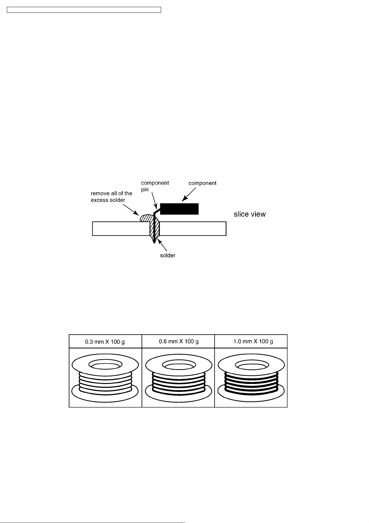
· When applying PbF solder to double layered boards, please check the component side for excess which may flow onto the
opposite side (See the figure below).
1.1. Suggested PbF Solder
There are several types of PbF solder available commercially. While this product is manufactured using Tin, Silver, and Copper
(Sn+Ag+Cu), you can also use Tin and Copper (Sn+Cu) or Tin, Zinc, and Bismuth (Sn+Zn+Bi). Please check the manufac
turer’s specific instructions for the melting points of their products and any precautions for using their product with other
materials. The following lead free (PbF) solder wire sizes are recommended for service of this product: 0.3 mm, 0.6 mm and
1.0 mm.
4
KX-TCD150FXB / KX-TCD150FXC / KX-TCD152FXB / KX-TCA115EXB / KX-TCA115EXC
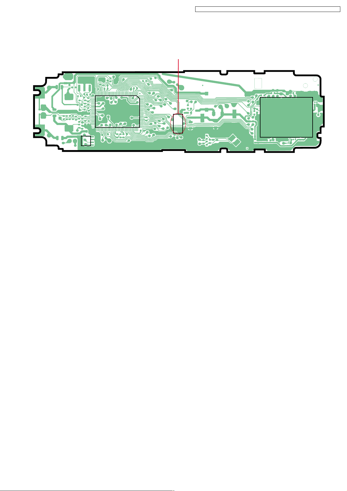
1.2. How to recognize that Pb Free solder is used
(Example: Handset P.C.B.)
Marked
30
31
IC1
50
51
8
1
IC2
4
5
1
100
PbF
81
80
(Component View)
Note:
The location of the “PbF” mark is subject to change without notice.
2 FOR SERVICE TECHNICIANS
ICs and LSIs are vulnerable to static electricity.
When repairing, the following precautions will help prevent recurring malfunctions.
1. Cover the plastic parts boxes with aluminum foil.
2. Ground the soldering irons.
3. Use a conductive mat on the worktable.
4. Do not touch IC or LSI pins with bare fingers.
3 CAUTION
10
IC3
17
1
26
1. Danger of explosion if battery is incorrectly replaced.
2. Replace only with the same or equivalent type recommended by the manufacturer.
3. Dispose of used batteries according to the manufacture’s Instructions.
5
KX-TCD150FXB / KX-TCD150FXC / KX-TCD152FXB / KX-TCA115EXB / KX-TCA115EXC
4 OPERATING INSTRUCTIONS
4.1. BATTERY
4.1.1. Battery Installation
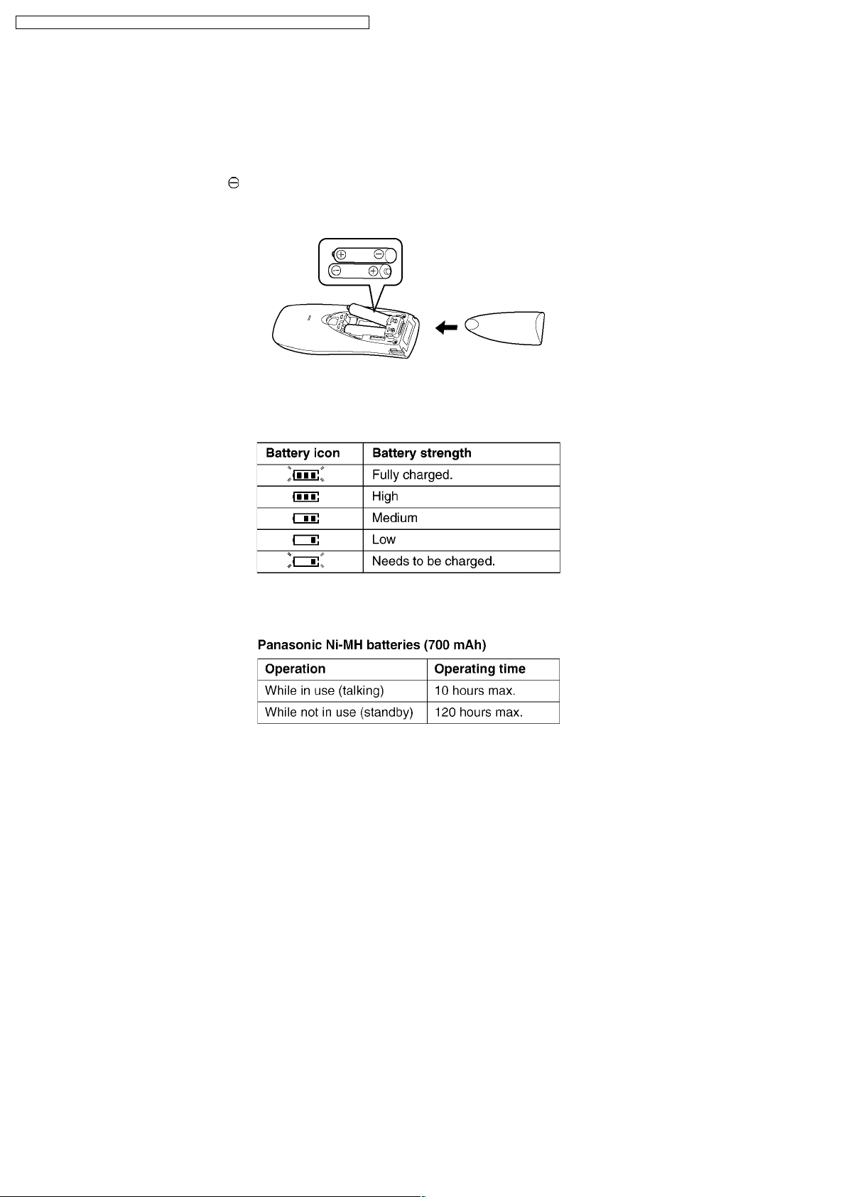
Insert the batteries negative ( ) terminal first. Close the handset cover.
Note:
· Use only rechargeable P03P (HHR-4EPT) batteries.
4.1.2. Battery Charge
Place the handset on the base unit for about 7 hours before initial use.
4.1.3. Battery Life
6
4.2. LOCATION OF CONTROLS
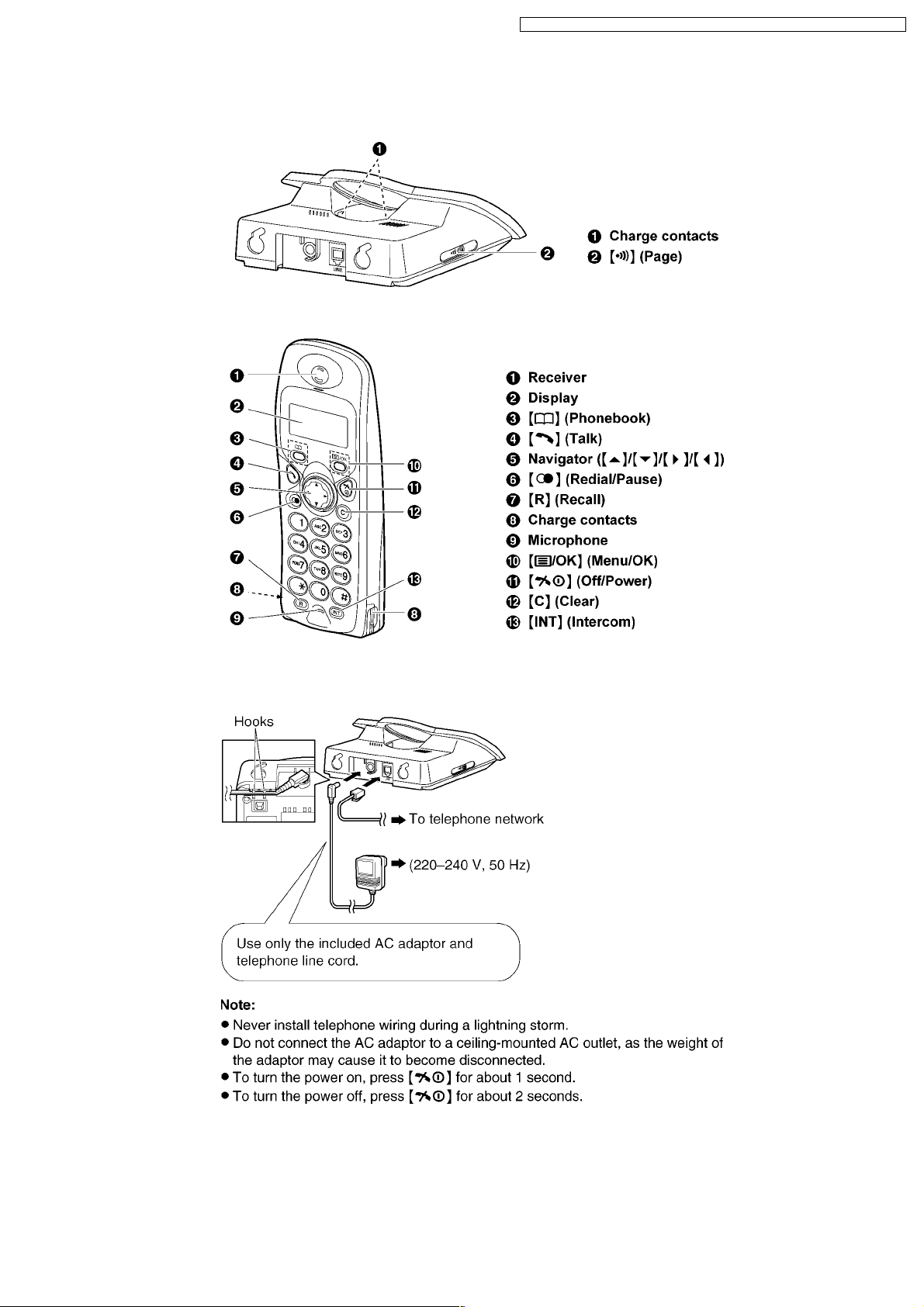
4.2.1. Base Unit
4.2.2. Handset
KX-TCD150FXB / KX-TCD150FXC / KX-TCD152FXB / KX-TCA115EXB / KX-TCA115EXC
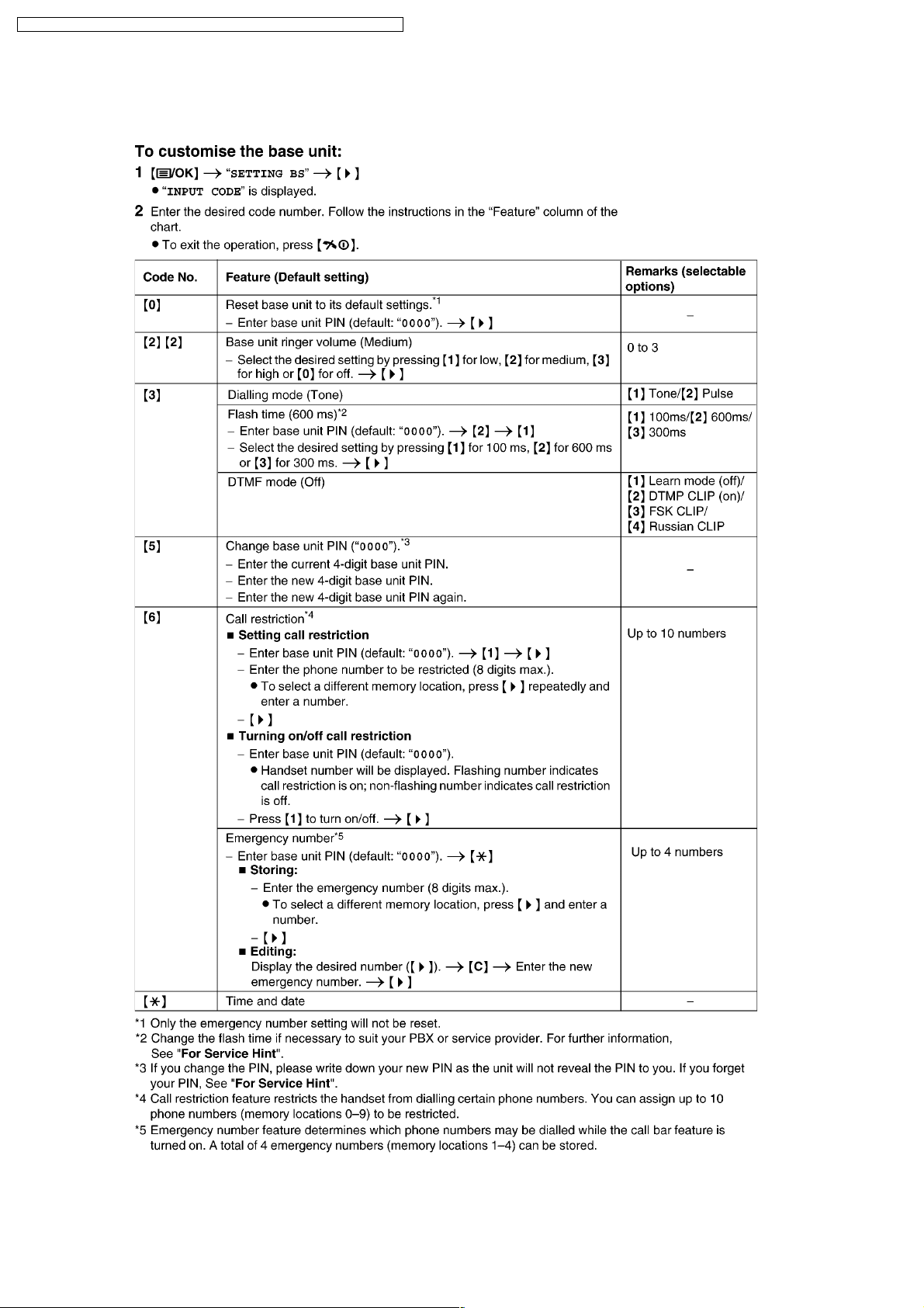
4.3. Connection
7
KX-TCD150FXB / KX-TCD150FXC / KX-TCD152FXB / KX-TCA115EXB / KX-TCA115EXC
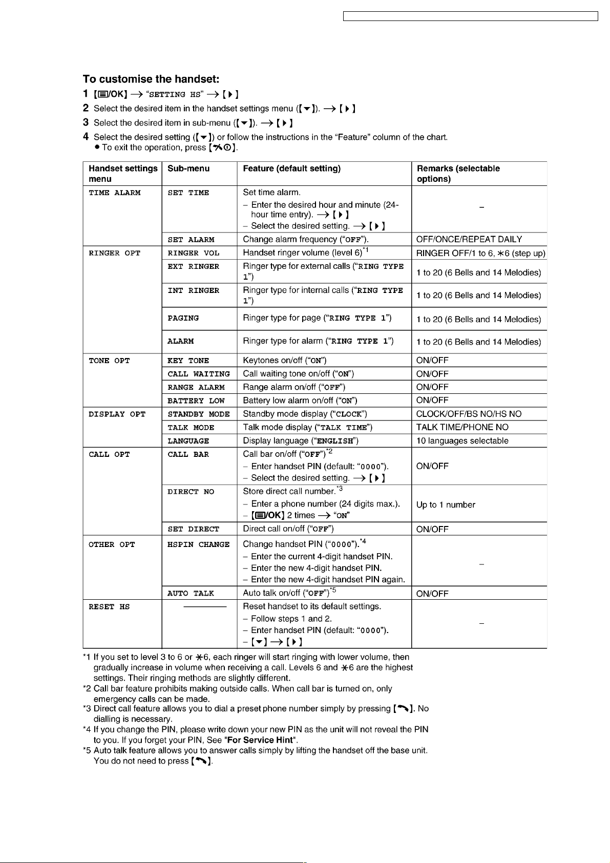
4.4. Guide to Settings
4.4.1. Base Unit
Cross Reference:
For Service Hint (P.10)
8
4.4.2. Handset
KX-TCD150FXB / KX-TCD150FXC / KX-TCD152FXB / KX-TCA115EXB / KX-TCA115EXC
Cross Reference:
For Service Hint (P.10)
9
KX-TCD150FXB / KX-TCD150FXC / KX-TCD152FXB / KX-TCA115EXB / KX-TCA115EXC
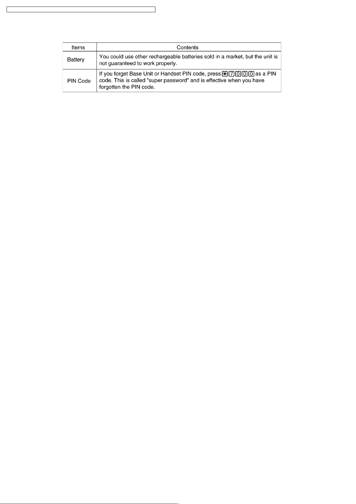
4.5. For Service Hint
10
5 DISASSEMBLY INSTRUCTIONS
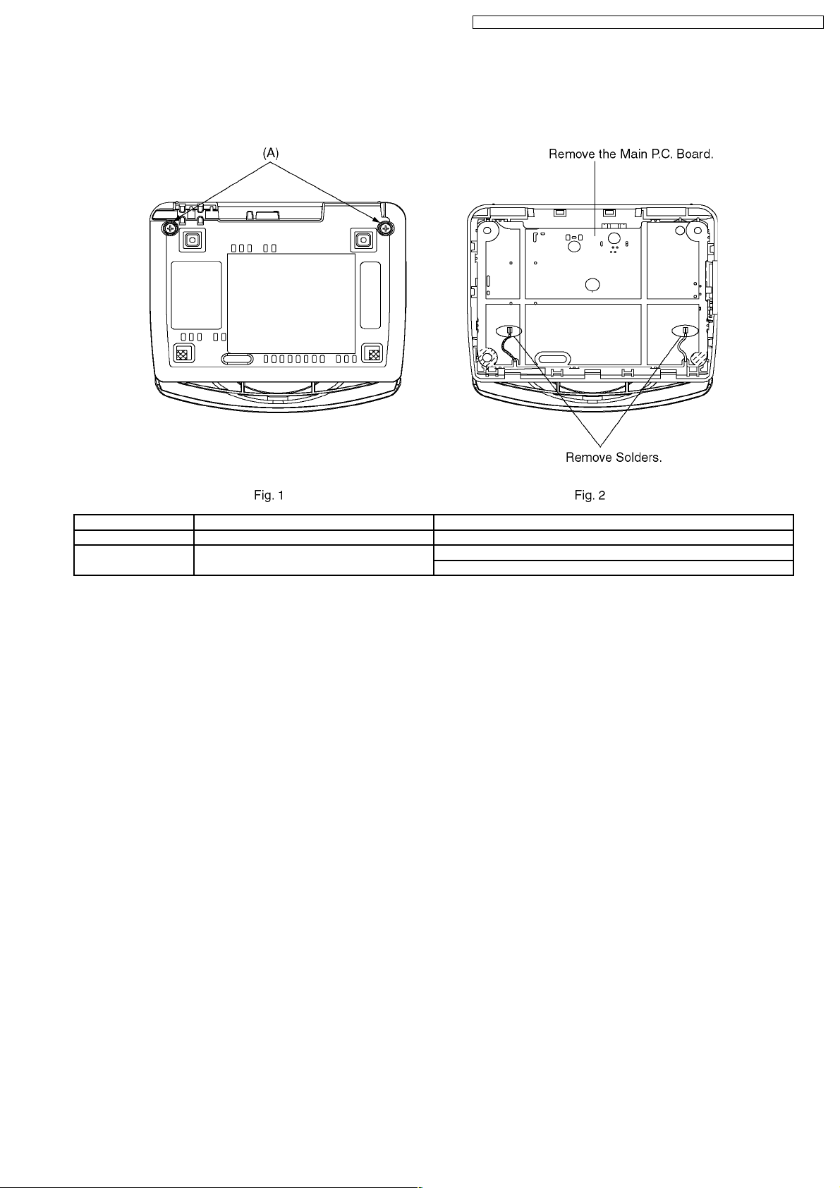
5.1. Base Unit
KX-TCD150FXB / KX-TCD150FXC / KX-TCD152FXB / KX-TCA115EXB / KX-TCA115EXC
Shown in Fig.- To Remove Remove
1 Lower Cabinet Screws (2.6 × 12)..........(A) × 2
2 Main P.C. Board Solders
Main P.C. Board
11
KX-TCD150FXB / KX-TCD150FXC / KX-TCD152FXB / KX-TCA115EXB / KX-TCA115EXC
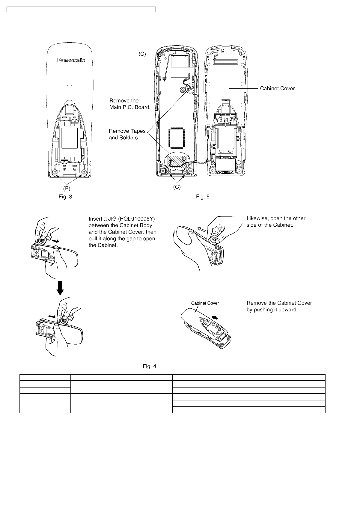
5.2. Handset
Shown in Fig.- To Remove Remove
3 Cabinet Cover Screws (2 × 8)..........(B) × 2
4 Follow the procedure.
5 Main P.C. Board Screw (2 × 8)..............(C) × 3
Tapes and Solders
Main P.C. Board
12
KX-TCD150FXB / KX-TCD150FXC / KX-TCD152FXB / KX-TCA115EXB / KX-TCA115EXC
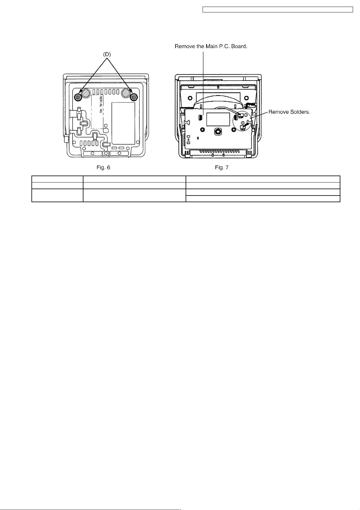
5.3. Charger Unit
Shown in Fig.- To Remove Remove
6 Lower Cabinet Screws (2.6 × 14)..........(D) × 2
7 Main P.C. Board Solders
Main P.C. Board
13
KX-TCD150FXB / KX-TCD150FXC / KX-TCD152FXB / KX-TCA115EXB / KX-TCA115EXC
6 ASSEMBLY INSTRUCTIONS
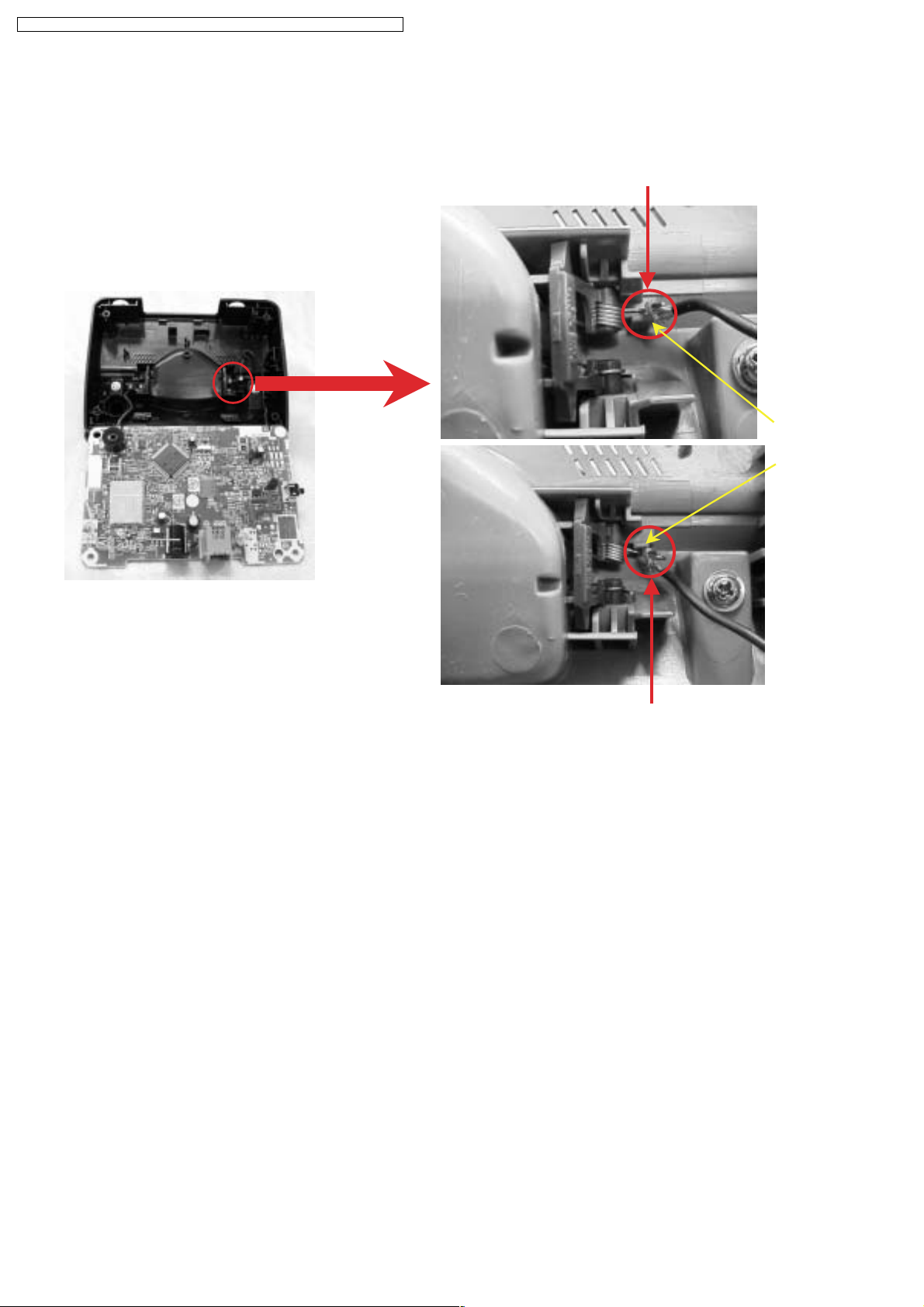
6.1. Warning When Constructing the Base Unit
OK
NG
CHG terminal is properly fit in the cabinet.
Rib
CHG terminal comes out of rib by pulling black lead wire when opening the cabinet and turning
the PCB over. The terminal cannot have enough elastic force, cannot have good contact with
handset, and it will result in charge problem.
14
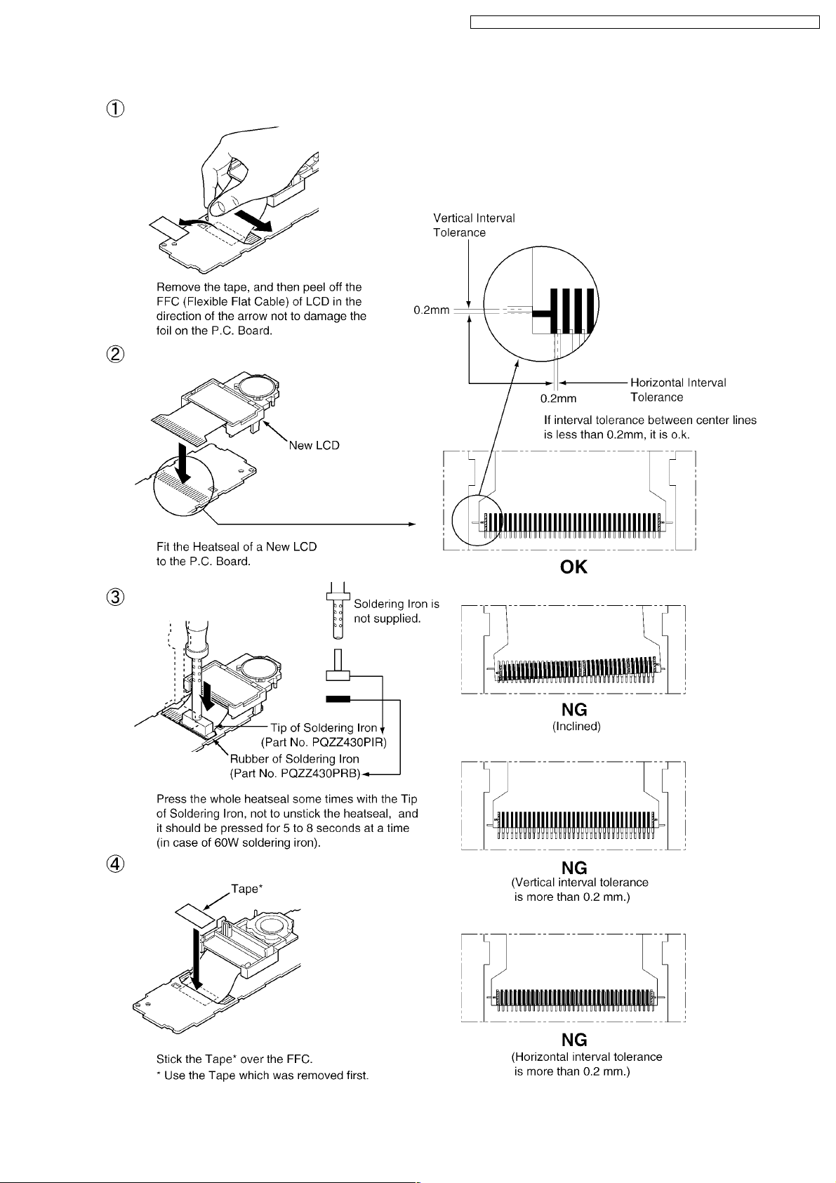
6.2. How to Replace the Handset LCD
KX-TCD150FXB / KX-TCD150FXC / KX-TCD152FXB / KX-TCA115EXB / KX-TCA115EXC
15
KX-TCD150FXB / KX-TCD150FXC / KX-TCD152FXB / KX-TCA115EXB / KX-TCA115EXC
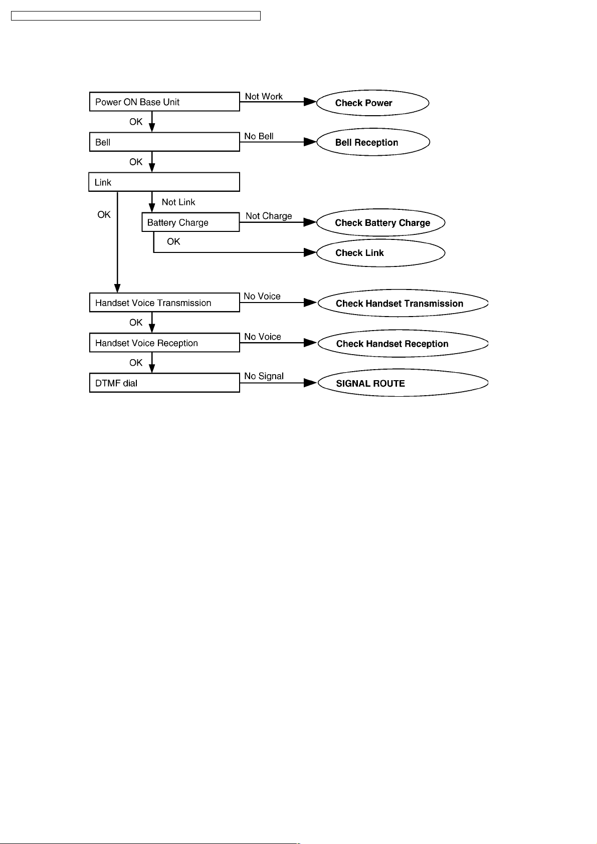
7 TROUBLESHOOTING GUIDE
Flow Chart
Cross Reference:
Check Power (P.17)
Bell Reception (P.22)
Check Battery Charge (P.18)
Check Link (P.19)
Check Handset Transmission (P.21)
Check Handset Reception (P.21)
SIGNAL ROUTE (P.46)
16
KX-TCD150FXB / KX-TCD150FXC / KX-TCD152FXB / KX-TCA115EXB / KX-TCA115EXC
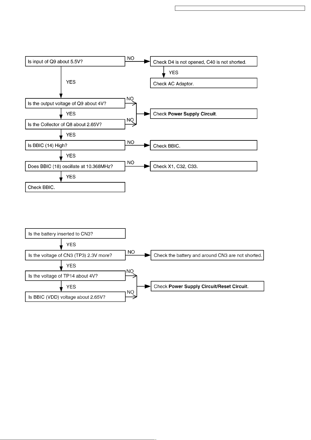
7.1. Check Power
7.1.1. Base Unit
Is the AC Adaptor inserted into AC outlet? (Check AC Adaptor’s specification.)
Cross Reference
Power Supply Circuit (P.41)
7.1.2. Handset
Cross Reference
Power Supply Circuit/Reset Circuit (P.44)
Note:
BBIC is IC2.
Note:
BBIC is IC1.
17
KX-TCD150FXB / KX-TCD150FXC / KX-TCD152FXB / KX-TCA115EXB / KX-TCA115EXC
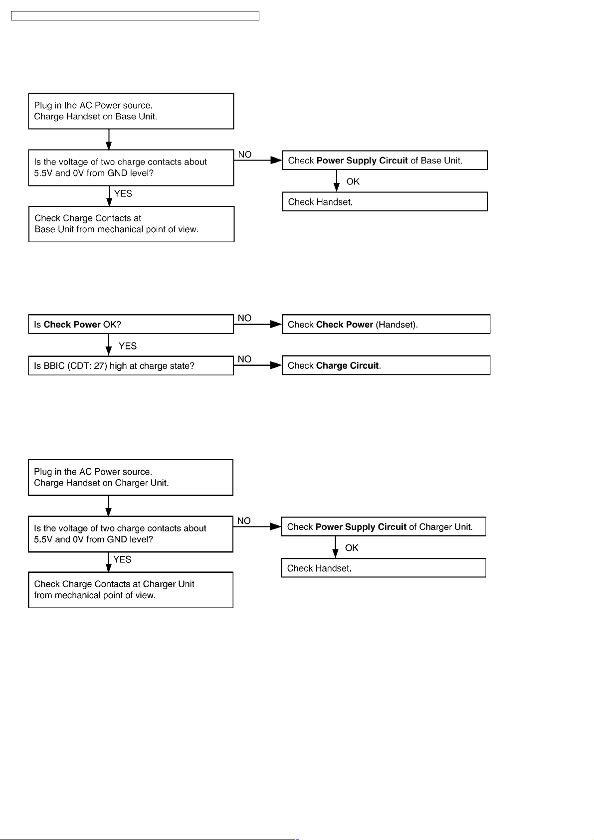
7.2. Check Battery Charge
7.2.1. Base Unit
Cross Reference:
Power Supply Circuit (P.41)
7.2.2. Handset
Cross Reference:
Check Power (P.17)
Charge Circuit (P.44)
7.2.3. Charger Unit
Cross Reference:
Power Supply Circuit (P.45)
Note:
BBIC is IC1.
18
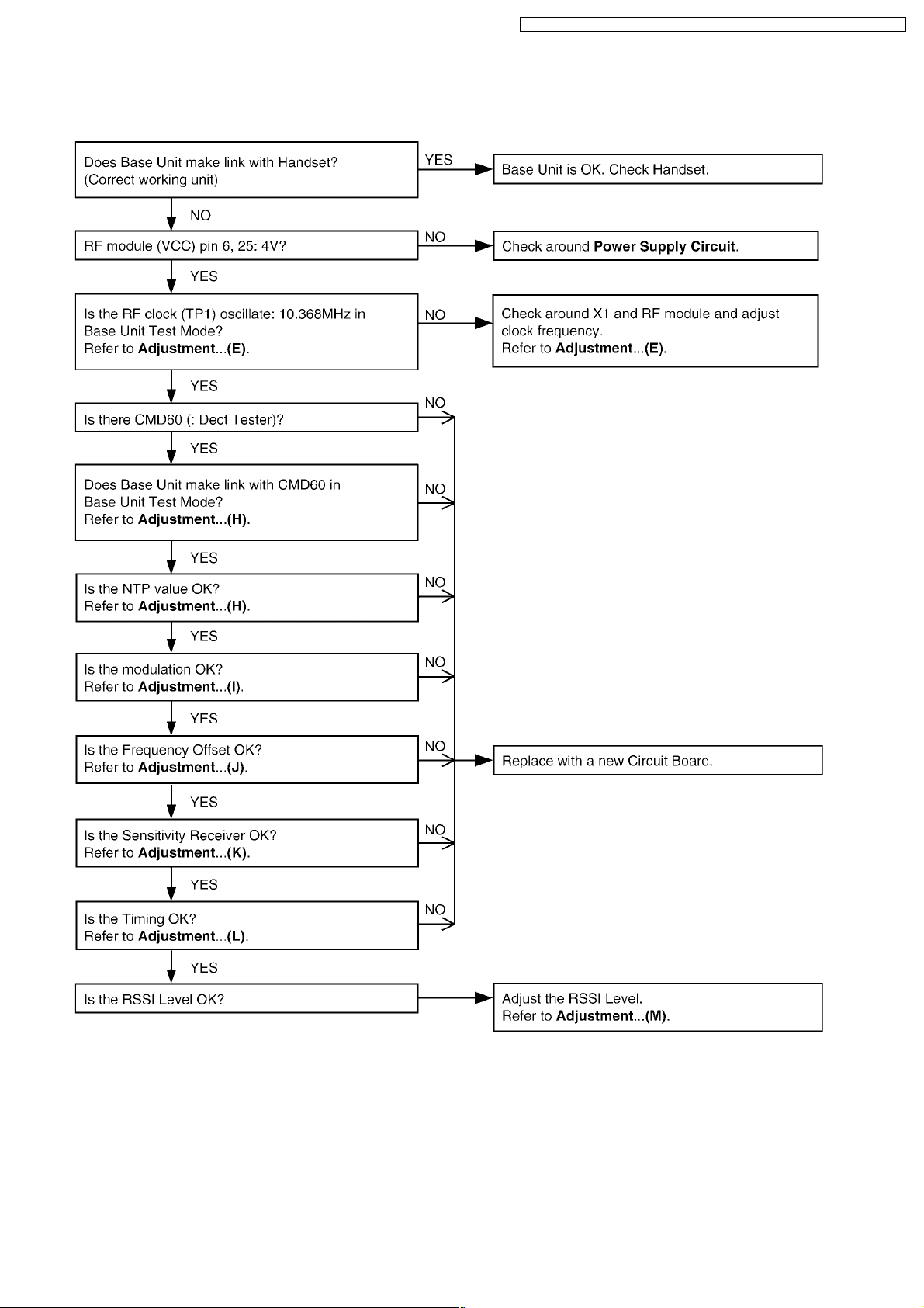
7.3. Check Link
7.3.1. Base Unit
KX-TCD150FXB / KX-TCD150FXC / KX-TCD152FXB / KX-TCA115EXB / KX-TCA115EXC
Cross Reference:
Power Supply Circuit (P.41)
Check Point (Base Unit) (P.23)
19
KX-TCD150FXB / KX-TCD150FXC / KX-TCD152FXB / KX-TCA115EXB / KX-TCA115EXC
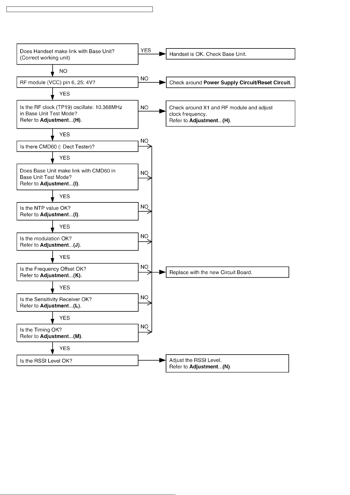
7.3.2. Handset
Cross Reference
Power Supply Circuit/Reset Circuit (P.44)
Check Point (Handset) (P.31)
20
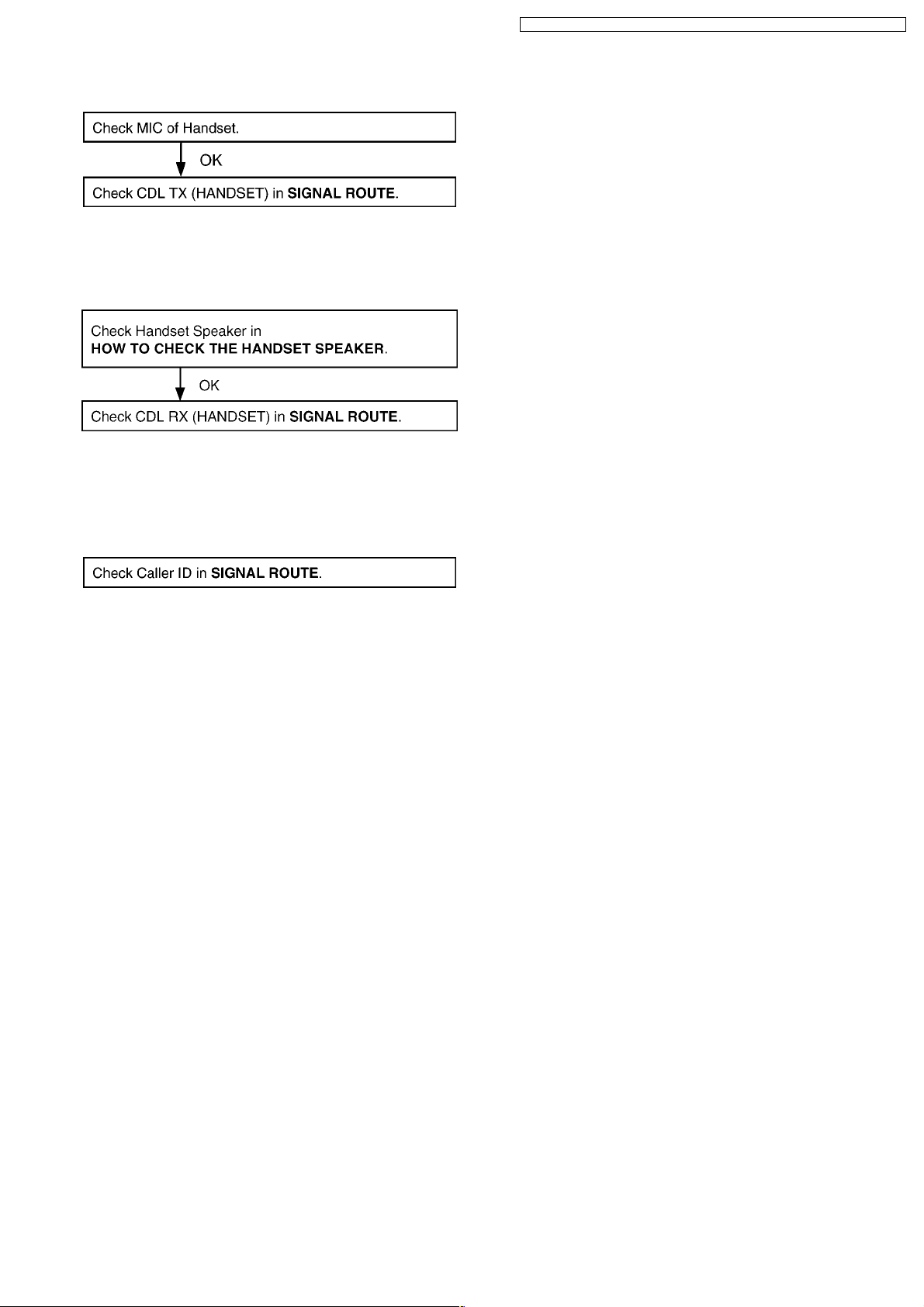
7.4. Check Handset Transmission
Cross Reference:
SIGNAL ROUTE (P.46)
7.5. Check Handset Reception
Cross Reference:
HOW TO CHECK THE HANDSET SPEAKER (P.37).
SIGNAL ROUTE (P.46)
KX-TCD150FXB / KX-TCD150FXC / KX-TCD152FXB / KX-TCA115EXB / KX-TCA115EXC
7.6. Check Caller ID
Cross Reference:
SIGNAL ROUTE (P.46)
21
KX-TCD150FXB / KX-TCD150FXC / KX-TCD152FXB / KX-TCA115EXB / KX-TCA115EXC
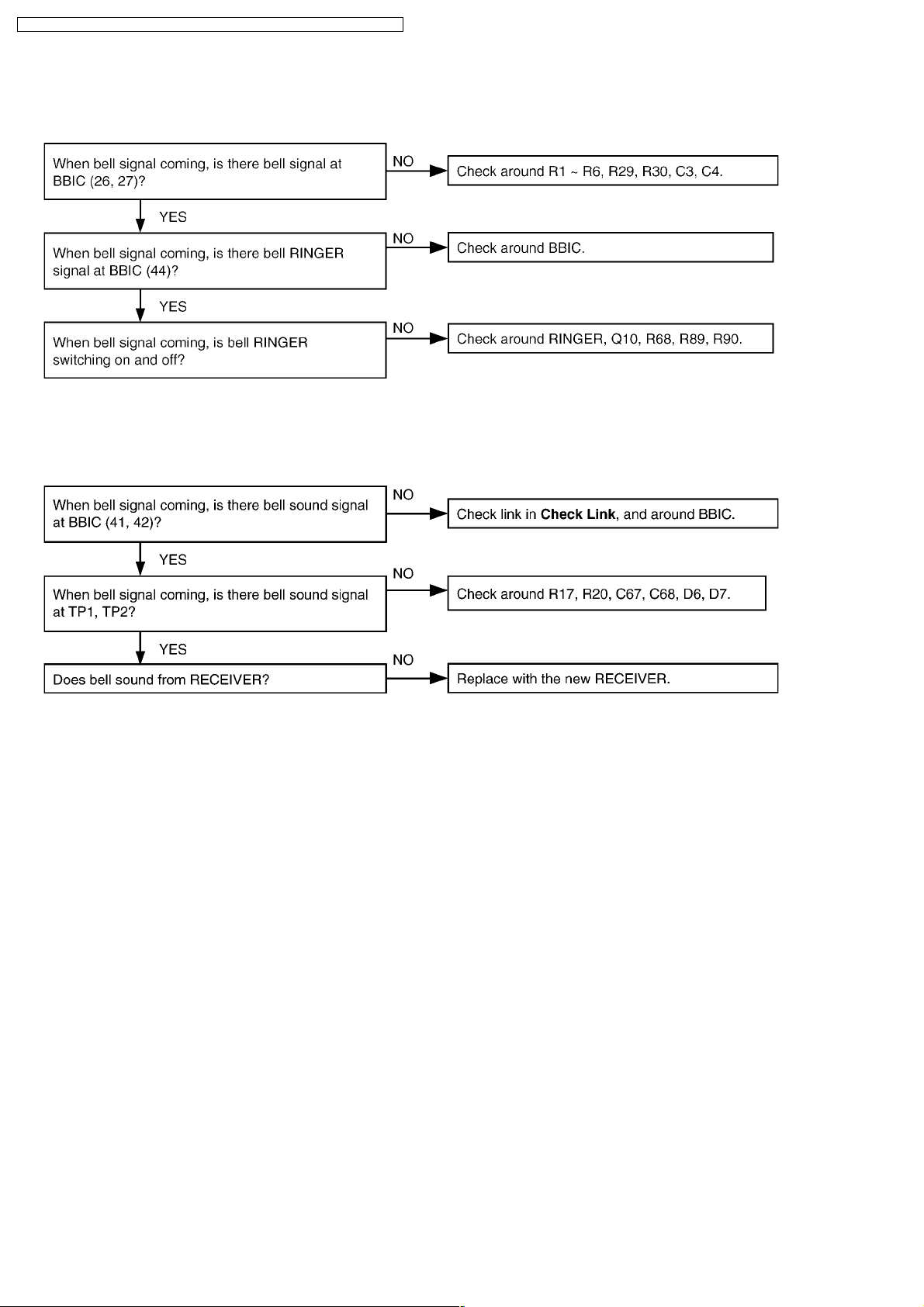
7.7. Bell Reception
7.7.1. Base Unit
Note:
BBIC is IC2.
7.7.2. Handset
Cross Reference:
Telephone Line Interface (P.42)
Check Link (P.19)
Note:
BBIC is IC1.
22
KX-TCD150FXB / KX-TCD150FXC / KX-TCD152FXB / KX-TCA115EXB / KX-TCA115EXC
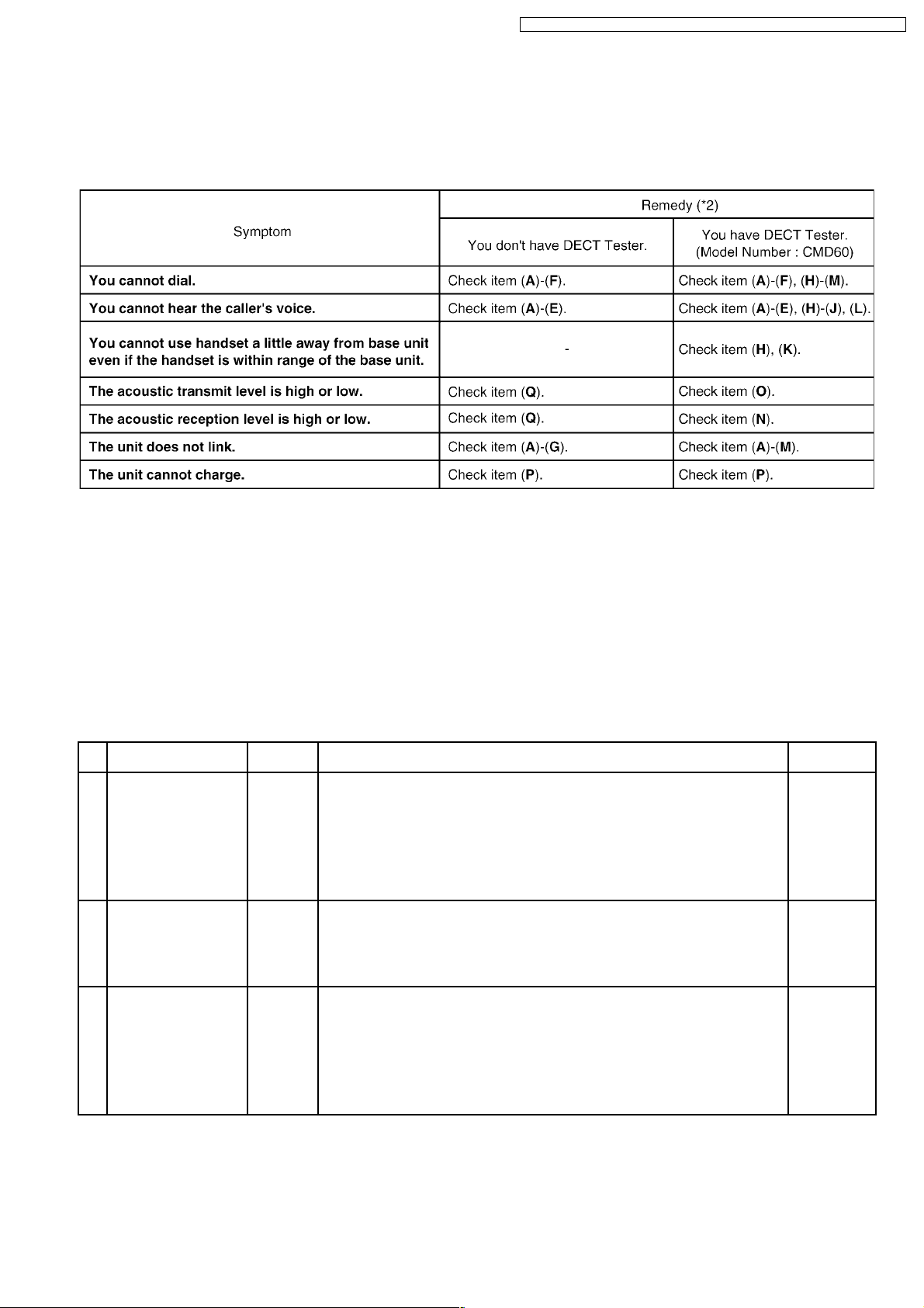
8 TROUBLESHOOTING BY SYMPTOM (BASE UNIT AND
CHARGER UNIT)
If your unit has below symptoms, follow the instructions in remedy column. Remedies depend on whether you have DECT
tester (*1) or not.
Note:
(*1) A general repair is possible even if you don’t have the DECT tester because it is for confirming the levels, such as
Acoustic level in detail.
(*2) Refer to Check Point (Base Unit) (P.23)
8.1. Check Point (Base Unit)
Please follow the items below when BBIC or EEPROM is replaced.
Note:
After the measuring, sock up the solder of TP.
*: PC Setting (P.27) is required beforehand.
The connections of simulator equipments are as shown in Adjustment Standard (Base Unit) (P.28).
Items Adjustment
(A) 2.65V Supply
Confirmation
(B) 4.0V Supply
Confirmation
(C) VBACK Status
Confirmation
Point
- 1. Confirm that the voltage between TP187 and GND is 2.65V ± 0.2V. IC2,Q8,C23,
- 1. Confirm that the voltage between TP91 and GND is 4.0V ± 0.2V. D4,C40,Q9,
- 1. Confirm that the voltage between J102 and GND is 0V ± 0.4V. IC2,Q8,C23,
Procedure Check or
Replace Parts
C24,C25,
C26,C27,C38,
R33,R36,
D5,C41,R41,
R42,Q9,
C40,D4,X1,
C32,C33,
C36,C37
R41,R42,
C41,D5,C75,
C78,C69,
C66,C67,C76,
IC3
C24,C25,
C26,C27,C38,
R33,R36,
D5,C41,R41,
R42,Q9,
C40,D4,R33,
X1,C32,
C33
23

KX-TCD150FXB / KX-TCD150FXC / KX-TCD152FXB / KX-TCA115EXB / KX-TCA115EXC
Items Adjustment
Procedure Check or
Point
(D)* BBIC Confirmation - 1. BBIC Confirmation (Execute the command “getchk”).
2. Confirm the returned checksum value.
Connection of checksum value and program number is shown below.
(E)* BBIC Clock Adjustment
(Important)
TP1 1. Execute the command “deactmac”.
2. Execute the command “conttx”.
3. Input Command “rdeeprom 00 00 02”, then you can confirm the current value.
4. Adjust the frequency of TP1 executing the command “setfreq 00 xx (where xx
is the value)” so that the reading of the frequency counter is 10.368000MHz ±
10Hz.
(F)* Hookswitch Check with
DC Characteristics
- 1. Connect J1 (Telephone Socket) to Tel-simulator which is connected with 600
Ω.
2. Set line voltage to 48V at on-hook condition and line current to 40mA at offhook condition of normal telephone.
3. Execute the command “hookoff”
4. Confirm that the line current is 40mA ± 5mA.
5. Execute the command “hookon”.
6. Confirm that the line current is 0mA + 2mA.
(G)* DTMF Generator
Confirmation
- 1. Connect J1 (Telephone Socket) to DTMF tester.
2. Execute the command “hookoff” and “dtmf_up”.
3. Confirm that the high frequency (1477.06Hz) group is -6.5dBm ~ -9.5dBm.
4. Execute the command “dtmf_lo”.
5. Confirm that the low frequency (852.05Hz) group is -9.0dBm ~ -12.0dBm.
(H)* Transmitted Power
Confirmation
- Remove the Antenna before starting steps from 1 to 5.
1. Configure the DECT tester (CMD60) as follows;
<Setting>
· Short TP10 and GND
· Test mode: FP
· Traffic Channel: 5
· Traffic Slot: 4
· Mode: Loopback
· PMID: 00000
2. Execute the command “testmode”.
3. Initiate connection from DECT tester. (“set up connect”)
4. Execute the command “ANT 1”.
5. Confirm that the NTP value at ANT is 20dBm ~ 25dBm.
(I) Modulation Check and
Adjustment
ANT Follow steps 1 to 3 of (H) above.
4. Confirm that the B-Field Modulation is 340kHz/div ~ 402kHz/div using data
type Fig31.
5. Adjust the B-Field Modulation if required. (Execute the command “readmod”
and “wrtmod xx”, where xx is the value.)
(J) Frequency Offset
Confirmation
- Follow steps 1 to 3 of (H) above.
4. Confirm that the frequency offset is -50kHz ~ +50kHz.
Replace Parts
IC2,X1,C32,
C33
IC2,IC3,L1,
C48,X1,C32,
C33
IC2,R7,R8,
R9,R10,R77,
Q2,Q3,D2,
C1,C2
IC2,R32,C22,
R23,C80,
C14,C13,Q6,
R22,R21,
R19,R20,C12,
D2,C1,
C2,R77,D3,
R12,Q2,
R7,R8,R9,
R10,Q3
IC2,IC3,L1,
C43,C78,
C75,C69,C48,
C72,C66,
C67,C76,C57,
C73,L3,
DA1,R66,R67,
C55,C56,
R78,R79,C54,
C58,C86,
R38
IC2,IC3,L1,
C43,C78,
C75,C69,C48,
C72,C66,
C67,C76,C57,
C73,L3,
DA1,R66,R67,
C55,C56,
R78,R79,C54,
C58,C86,
R38
IC2,IC3,L1,
C43,C78,
C75,C69,C48,
C72,C66,
C67,C76,C57,
C73,L3,
DA1,R66,R67,
C55,C56,
R78,R79,C54,
C58,C86,
R38
24
 Loading...