

ORDER NO. KMS0307792C3
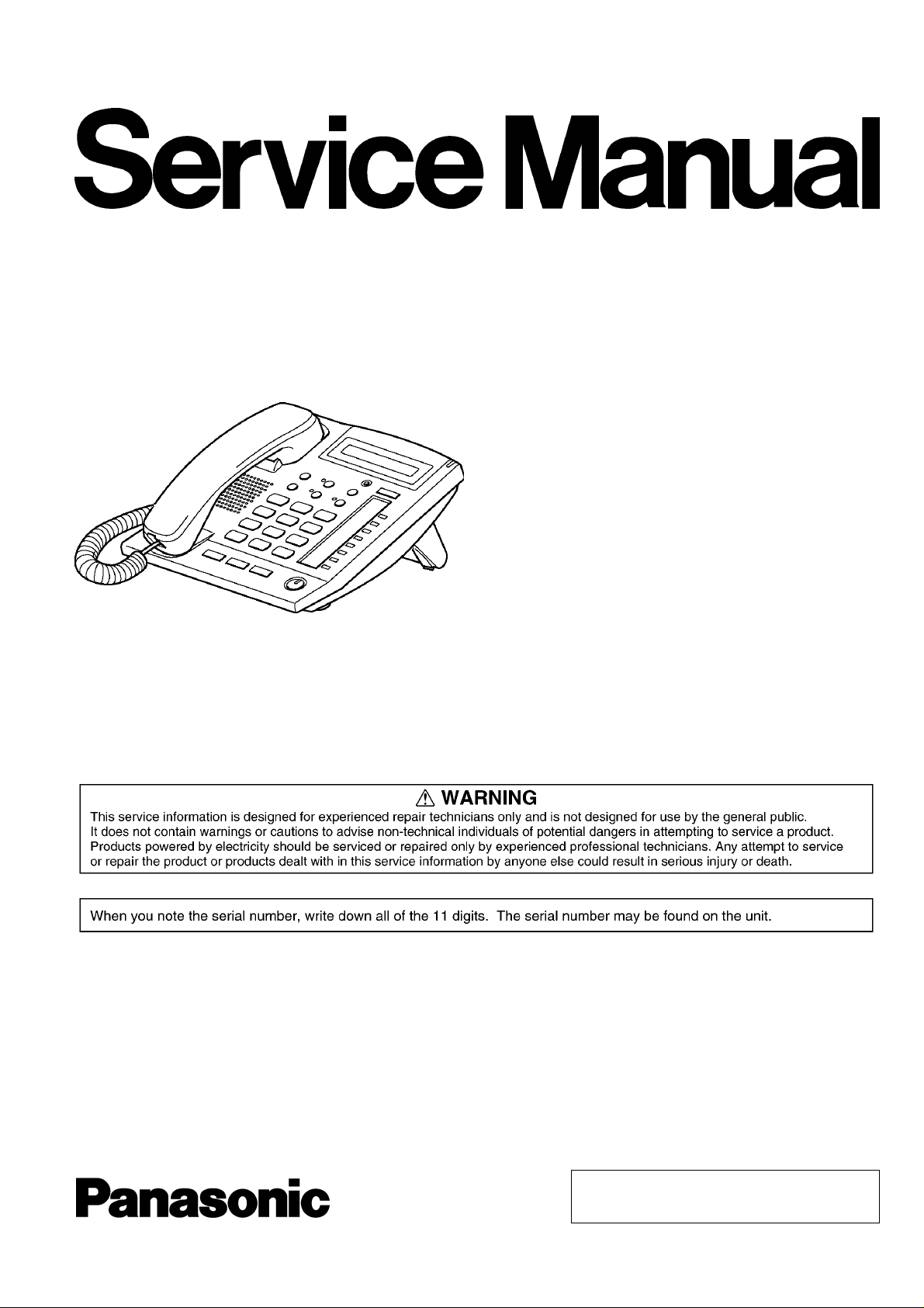
Digital Proprietary Telephone
KX-T7665AL
KX-T7665X
(for Australia, Asia, Middle Near East, Africa and Latin
America)
IMPORTANT INFORMATION ABOUT LEAD FREE, (PbF), SOLDERING
If lead free solder was used in the manufacture of this product the printed circuit boards will be marked PbF.
Standard leaded, (Pb), solder can be used as usual on boards without the PbF mark.
When this mark does appear please read and follow the special instructions described in this manual on the use of PbF and how
it might be permissible to use Pb solder during service and repair work.
© 2003 Panasonic Communications Co., Ltd. All
rights reserved. Unauthorized copying and
distribution is a violation of law.

KX-T7665AL / KX-T7665X
CONTENTS
Page Page
1 ABOUT LEAD FREE SOLDER (PbF: Pb free) 3
1.1. SUGGESTED PbF SOLDER
1.2. HOW TO RECOGNIZE THAT Pb FREE SOLDER IS
USED
2 FOR SERVICE TECHNICIANS
3 SPECIFICATIONS
4 LOCATION OF CONTROLS
5 CONNECTION
6 DISASSEMBLY INSTRUCTIONS
7 HOW TO REPLACE A FLAT PACKAGE IC
7.1. PREPARATION
7.2. PROCEDURE
7.3. REMOVING SOLDER FROM BETWEEN PINS
8 TROUBLESHOOTING GUIDE
8.1. NO OPERATION
8.2. LCD DOES NOT OPERATE
8.3. HANDSET DOES NOT WORK
8.4. SPEAKER-PHONE TROUBLE
8.5. DXDP-DPT DOES NOT WORK
9 BLOCK DIAGRAM
10 CIRCUIT OPERATIONS
10.1. KEY INPUT CONTROL CIRCUIT
10.2. LCD CONTROL CIRCUIT
10
11
12
13
14
15
15
16
3
4
5
5
5
6
7
8
8
8
8
9
9
10.3. LED CIRCUIT
10.4. RESET CIRCUIT
10.5. POWER SUPPLY CIRCUIT
10.6. DATA COMMUNICATION
10.7. DXDP COMMUNICATION
10.8. ANALOG CIRCUIT
11 IC DATA
11.1. IC2
11.2. IC6
12 TER MINAL GUIDE OF ICs, TRANSISTORS AND DIODES
13 CABINET AND ELECTRICAL PARTS LOCATION
14 ACCESSORIES AND PACKING MATERIALS
15 REPLACEMENT PARTS LIST
15.1. CABINET AND ELECTRICAL PARTS
15.2. ACCESSORIES AND PACKING MATERIALS
15.3. MAIN BOARD PARTS
16 FOR THE SCHEMATIC DIAGRAM
17 SC HEMATIC DIAGRAM
18 WAVEFORM
19 PRINTED CIRCUIT BOARD (MAIN BOARD)
19.1. COMPONENT VIEW
19.2. BOTTOM VIEW
17
18
18
19
20
21
23
23
25
26
27
28
29
29
29
29
31
32
34
37
37
38
2
KX-T7665AL / KX-T7665X
1 ABOUT LEAD FREE SOLDER (PbF: Pb free)
Note:
In the information below, Pb, the symbol for lead in the periodic table of elements, will refer to standard solder or solder that
contains lead.
We will use PbF solder when discussing the lead free solder used in our manufacturing process which is made from Tin, (Sn),
Silver, (Ag), and Copper, (Cu).
This model, and others like it, manufactured using lead free solder will have PbF stamped on the PCB. For service and repair
work we suggest using the same type of solder although, with some precautions, standard Pb solder can also be used.
Caution
· PbF solder has a melting point that is 50° ~ 70° F, (30° ~ 40°C) higher than Pb solder. Please use a soldering iron with
temperature control and adjust it to 700° ± 20° F, (370° ± 10°C). In case of using high temperature soldering iron, please
be careful not to heat too long.
· PbF solder will tend to splash if it is heated much higher than its melting point, approximately 1100°F, (600°C).
· If you must use Pb solder on a PCB manufactured using PbF solder, remove as much of the original PbF solder as possible
and be sure that any remaining is melted prior to applying the Pb solder.
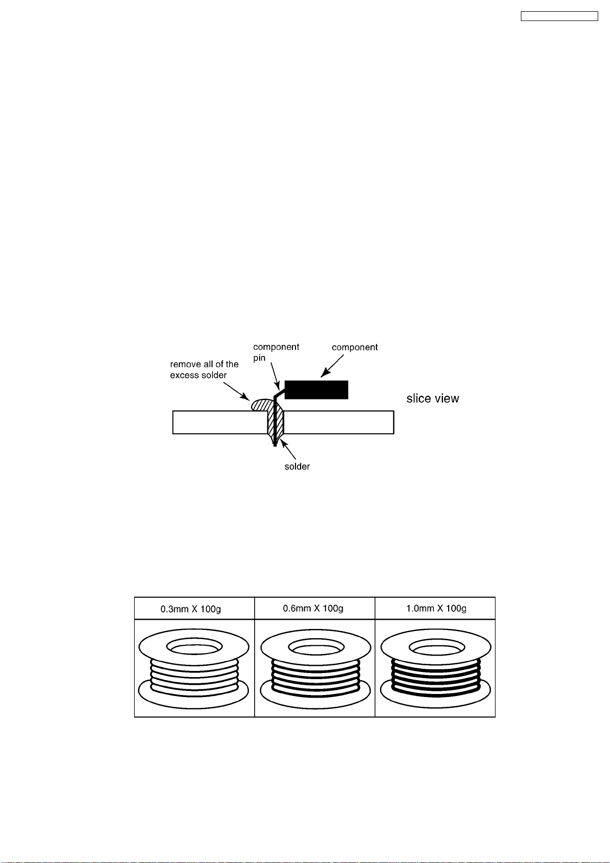
· When applying PbF solder to double layered boards, please check the component side for excess which may flow onto the
opposite side (See figure, below).
1.1. SUGGESTED PbF SOLDER
There are several types of PbF solder available commercially. While this product is manufactured using Tin, Silver, and Copper,
(Sn+Ag+Cu), you can also use Tin and Copper, (Sn+Cu), or Tin, Zinc, and Bismuth, (Sn+Zn+Bi).
Please check the manufacturer’s specific instructions for the melting points of their products and any precautions for using their
product with other materials.
The following lead free (PbF) solder wire gauges are recommended for service of this product: 0.3mm, 0.6mm and 1.0mm.
3
KX-T7665AL / KX-T7665X
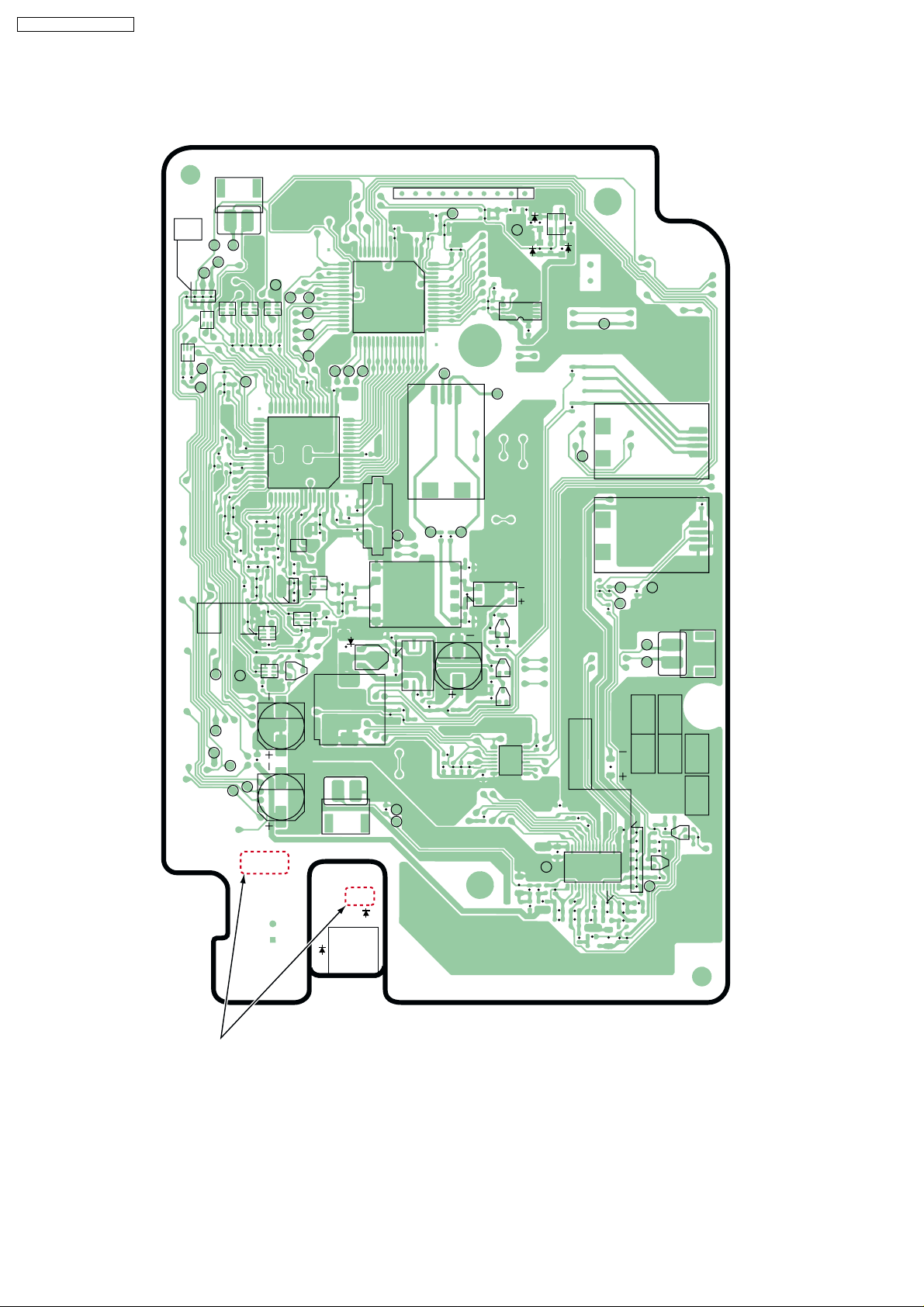
1.2. HOW TO RECOGNIZE THAT Pb FREE SOLDER IS USED
PbF is stamped to show that Pb free solder is used. (See the figure below.)
R
W
R306
A1
R310
Q32
R308
R309
R311
A6
Q31
A3
R307
A4
R516
C104
C103
R100
B3
B2
B1
2
R519
R520
R119
C107
R112
R115
A5
1
B6
A2
Q33 Q34 Q35
R305
R302
R301
R303
R402
PN9
17
R521
R517
R406
R129
C401
32
R116
R114
C101
R113
C108
R110
C105
R109
R111
R117
C106
C114
C120
Q3
R136
R135
Q5
D3V
C117
R200
F5
F7
PSUP1439Z-A
PbF
CN3
B5
E2
R304
R300
R407
16
IC2
33 48
C407
R103
R102
C100
C406
R101
R106
R105
IC7
R108
C102
R107
R104
C113
Q2
R134
R133
R139
R138
Q6
R137
C204
C205
C607
C606
16
17
E1
F8
32 49
F6
33 48
F4
F2
F1
F3
C400
1
64
C403
49
R403
R132
C115
R401
R130
D21
Q21
L21
CN2
R400
C111
C109
C404
C405
R131
5
21
X1
C201
W
C402
Q1
C116
R
PSUP1439Z-B
PbF
D43
10
IC6
D44
B4
R202
R201
C200
C505
R610
1
T1
IC1
R208
R204
AG2
MIC2
R601
C602
64
H
R209
R518
G1
R602
JK1
L1
C203
C202
R526
CN5
C605
T
L
L2
101
9
R206
R515
R604
R603
R611
R609
R608
C118
C112
R524
C110
R207
R525
R600
D5V
D1
R140
R119
R203
R205
C522
R513
R607
R
R114
IC3
C601
IC5
Q4
R142
Q22
Q23
C524
1
C600
C609
GND
R506
R512
C514
R505
D63
D62
C523
C528
C516
C506
R511
IC8
C603
D61
E3
R514
C515
R507
C604
L3
L4
R605
C608
R606
R503
C503
C510
C521
C508
C507
C517
IC4
C519
C502
R502
E4
L51
R527
C518
C511
C520
C512
L52
MIC1
C525
R510
C526
SP1
SPN
SPP
C509
R509
R500
R501
JK2
JK3
C501
RU CNGen
C513
AG1
W
R
R523
R504
C504
R508
A3V
2
1
C527
Q51
C500
CN1
GRA
DB
Q52
R522
Marked PbF
A
KX-T7665AL / KX-T7665X : MAIN BOARD
4

2 FOR SERVICE TECHNICIANS
ICs and LSIs are vulnerable to static electricity.
When repairing, the following precautions will help prevent recurring malfunctions.
1. Cover the plastic parts boxes with aluminum foil.
2. Ground the soldering irons.
3. Use a conductive mat on the worktable.
4. Do not touch IC or LSI pins with bare fingers.
3 SPECIFICATIONS
Station Loop Limit: 90 ohms
Calling Method: 2 pair wire
Jacks: Handset Jack, TEL Jack
Dimensions: Low Angle:
High Angle:
Weight: 0.7 kg
213 (D)mm × 177 (W)mm × 107 (H)mm
201 (D)mm × 177 (W)mm × 127 (H)mm
KX-T7665AL / KX-T7665X
Design and specifications are subject to change without notice.
4 LOCATION OF CONTROLS
5

KX-T7665AL / KX-T7665X
5 CONNECTION
Caution:
The availability of D-XDP function depends on the software version of the connected Business Telephone System.
Consult your dealer for more details about D-XDP.
6
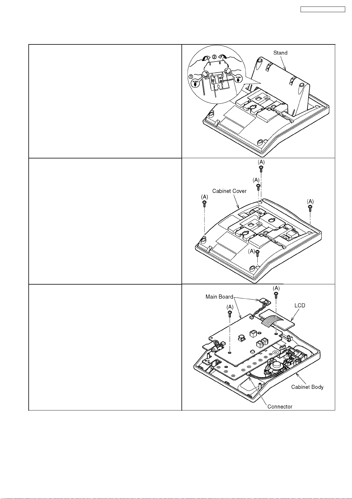
6 DISASSEMBLY INSTRUCTIONS
1. Remove the Stand.
2. Remove 5 Screws (A).
3. Remove the Cabinet Cover.
KX-T7665AL / KX-T7665X
4. Remove the Connector from the Main Board.
5. Remove 2 Screws (A).
6. Remove the Main Board and the LCD from the Cabinet Body.
7
KX-T7665AL / KX-T7665X
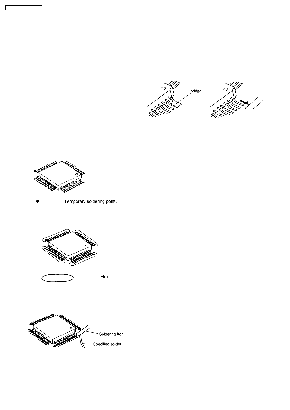
7 HOW TO REPLACE A FLAT PACKAGE IC
7.1. PREPARATION
· PbF (: Pb free) Solder
· Soldering Iron
Tip Temperature of 700°F±20°F (370°C±10°C)
Note: We recommend a 30 to 40 Watt soldering iron. An
expert may be able to use a 60 to 80 Watt iron where
someone with less experience could overheat and damage
the PCB foil.
· Flux
Recommended Flux: Specific Gravity → 0.82.
Type → RMA (lower residue, non-cleaning type)
Note: See ABOUT LEAD FREE SOLDER (PbF: Pb free)
(P.3).
7.2. PROCEDURE
1. Tack the flat pack IC to the PCB by temporarily soldering
two diagonally opposite pins in the correct positions on the
PCB.
7.3. REMOVING SOLDER FROM
BETWEEN PINS
1. Add a small amount of solder to the bridged pins.
2. With a hot iron, use a sweeping motion along the flat part of
the pin to draw the solder from between the adjacent pads.
Be certain each pin is located over the
correct pad on the PCB.
2. Apply flux to all of the pins on the IC.
3. Being careful to not unsolder the tack points, slide the
soldering iron along the tips of the pins while feeding
enough solder to the tip so that it flows under the pins as
they are heated.
8
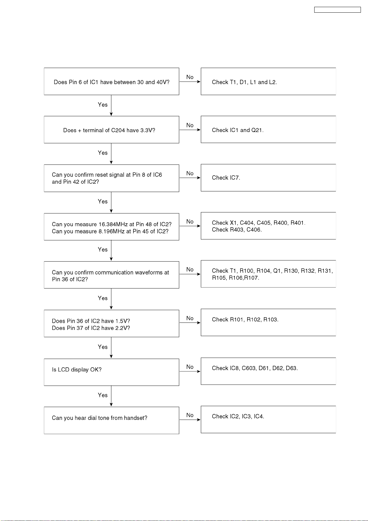
8 TROUBLESHOOTING GUIDE
8.1. NO OPERATION
KX-T7665AL / KX-T7665X
Note:
Refer to (1)~(4) of WAVEFORM (P.34) for waveform.
9
KX-T7665AL / KX-T7665X
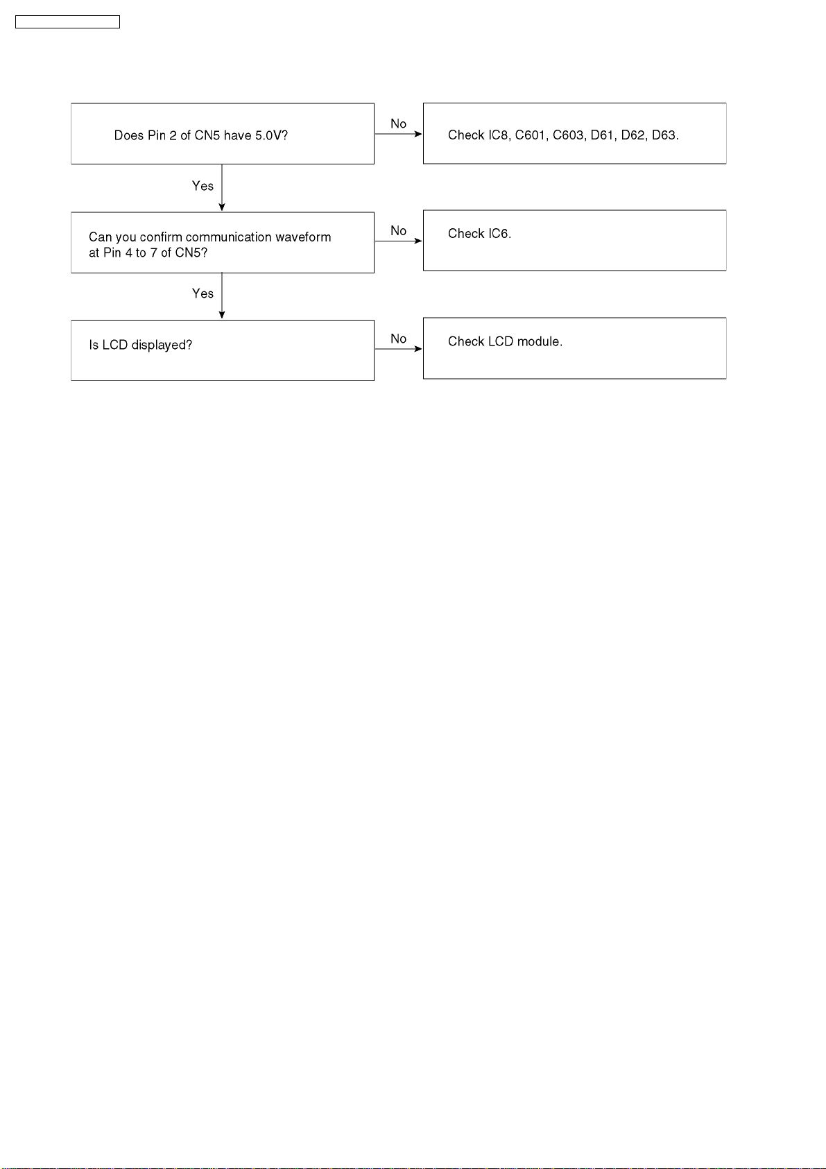
8.2. LCD DOES NOT OPERATE
Note:
Refer to (5)ofWAVEFORM(P.34) for waveform.
10
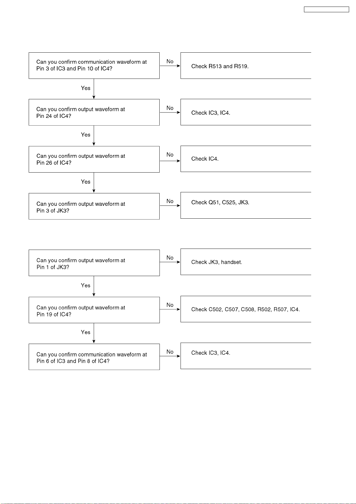
8.3. HANDSET DOES NOT WORK
Receive
KX-T7665AL / KX-T7665X
Send
Note:
Refer to (6)~(7) of WAVEFORM (P.34) for waveform.
11
KX-T7665AL / KX-T7665X
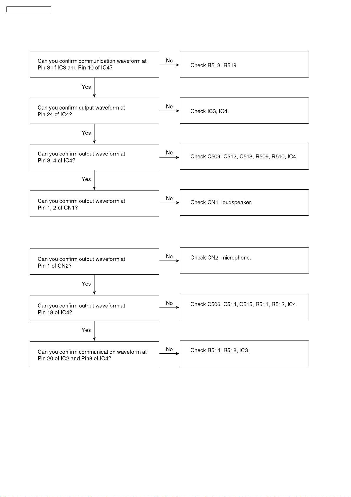
8.4. SPEAKER-PHONE TROUBLE
Receive
Send
Note:
Refer to (6)~(7) of WAVEFORM (P.34) for waveform.
12
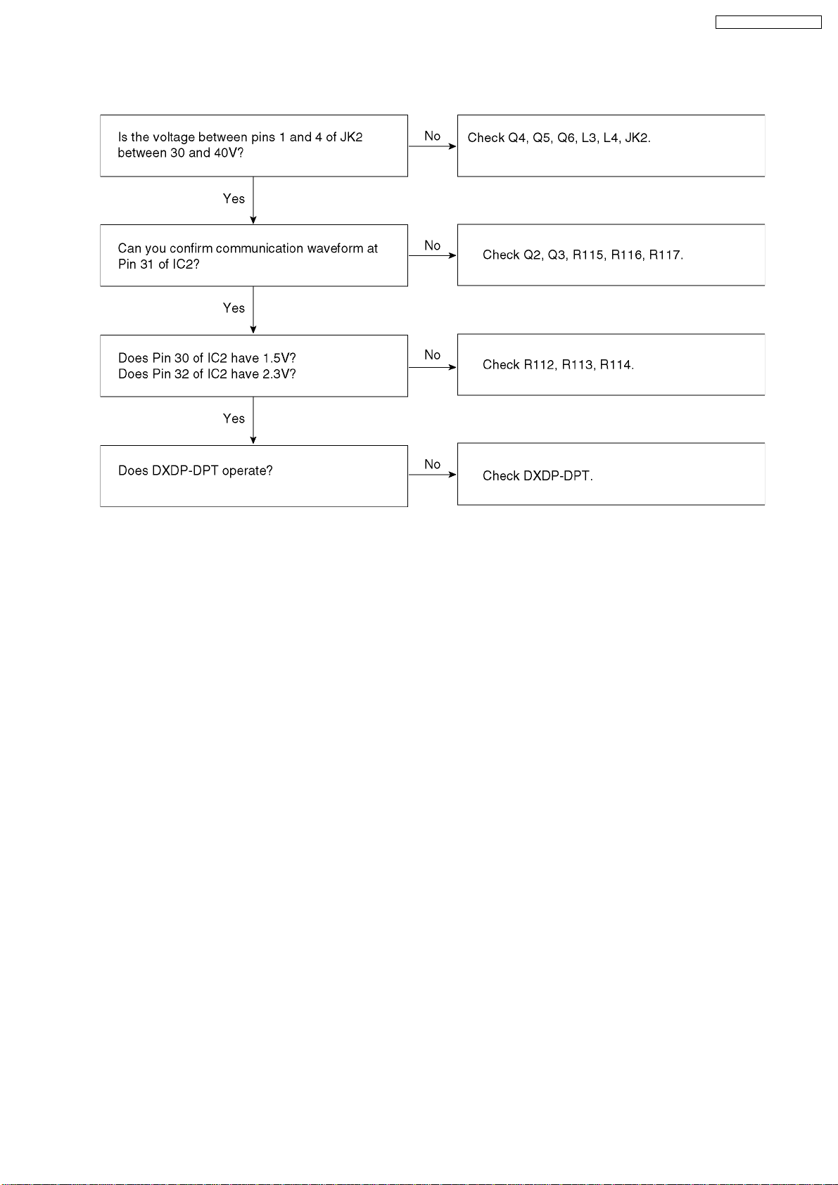
8.5. DXDP-DPT DOES NOT WORK
KX-T7665AL / KX-T7665X
Note:
Refer to (8)ofWAVEFORM(P.34) for waveform.
13

KX-T7665AL / KX-T7665X
JK1
TEL Jack
T1
Q1
Data
Communication
PDX1
PDX0
PDR
JK2
Q4
Q2
Q3
Data
Communication
DDX1
DDX0
DXDP Jack
Q6
Q5
DDR
Power
D3V
IC1
A3V
Q21,L21
LED
D43
CN3-CN4
D44
LED
3
~
5
~
CLM0
NROW0
D32~D42
Q31~Q35
KX-T7665AL / KX-T7665X : BLOCK DIAGRAM
OSR
OSX
DXDRBCLK
OEP0
OCK
Phone
Speaker
FS
IC4
CODEC
IC3
X1
SCK,DATA
Tone
ASIC
Reset
SCL,SDA
IC2
IC7
5
7
~
~
DB0
ADR0
IC6
CPU
7
~
E,W,RS
LCD-D4
WEN,REN,INTN
5.0V
IC8,D63
3.3V
Hook SW
Key
SW1~32
9 BLOCK DIAGRAM
JK3
H/S Jack
SP
CN1
MIC
CN2
IC5
EEPROM
14
TO
LCD
MAIN P. C. Board
(CN5)

10 CIRCUIT OPERATIONS
10.1. KEY INPUT CONTROL CIRCUIT
The key data is under the matrix control by 20 to 23(KEYOUT) and 28 to 35(KEYIN) of IC6.
The key information outputted from KEYOUT is inputted into KEYIN, when the key is pressed.
KX-T7665AL / KX-T7665X
15

KX-T7665AL / KX-T7665X
10.2. LCD CONTROL CIRCUIT
The LCD data is output from pins 52 to 58 of IC6.
LCD contrast adjustment is performed by the circuit composed of R603 and R604.
The contrast is determined only by the voltage level between pin 2 and pin 3 of CN5. Higher potential makes the contrast high.
CONTRAST IC6 Pin 59 IC6 Pin19
HIGH L L
MIDDLE Z L
LOW Z Z
LCD Contrast Control
16

10.3. LED CIRCUIT
The lighting of the LED is controlled by pin 14 to 18 (Row) and pin 8 to 13 (Colum) of IC2.
The LED lights up in a dynamic lighting system.
The duty ratio is 1/8 (ON time 1.5ms).
KX-T7665AL / KX-T7665X
17

KX-T7665AL / KX-T7665X
10.4. RESET CIRCUIT
Reset Signal is outputted from IC7 and inputted into IC2, IC3 and IC6 at the connection of TEL cord.
10.5. POWER SUPPLY CIRCUIT
This circuit converts the voltage supplied from PBX into the power supply voltage of +3.3V by IC1 (Switching Regulator IC).
Q22 and Q23 control the power supply circuit as below to turn IC1 on in low consumption current at starting up.
· Input Voltage approx. 26V or less →Q23 OFF →Q22 ON →IC1-pin 3 H →IC1 OFF
· Input Voltage approx. 26V or more →Q23 ON →Q22 OFF →IC1 ON
18

KX-T7665AL / KX-T7665X
10.6. DATA COMMUNICATION
Function
The data communication circuit serves the following functions:
Information exchanger between PBX and proprietary telephone, key input information as well as data for the LED control, LCD
control, voice data, etc. This information is continuously exchanged at all times.
Circuit Operation
The data received from PBX is inputted to the comparator (pin 36) built in IC2 through Pulse Trans T1. The threshold voltage
of the comparator is determined by R101 to 103 and inputted to pin 37 and 35 of IC2.
The data to PBX is outputted from pin 38 and 39 of IC2, drives T1 by Transistor Q1 and transmitted.
19

KX-T7665AL / KX-T7665X
10.7. DXDP COMMUNICATION
Function
This circuit performs the same communication as DXDP-compatible DPT and PBX communication connected with DXDP port.
Circuit Operation
The data to Slave DPT is outputted from pin 33 and 34 of IC2 and sent by Transistor Q2 and Q3.
The data from Slave DPT is inputted to the comparator (pin 31) built in IC2.
The threshold voltage of the comparator is determined by R112 to 114 and inputted to pin 30 and 32 of IC2.
Also, the supplying power to Slave DPT is controlled by a constant current circuit of Q16 as below.
· IC2-pin 28 as H : Constant current circuit ON
· IC2-pin 28 as L : Constant current circuit OFF
· IC2-pin 29 as H : 40mA Feeding (Slave DPT usually)
· IC2-pin 29 as L : 20mA Feeding (Slave DPT at starting up only)
20

10.8. ANALOG CIRCUIT
This circuit performs the setting of the call path/vol. adjustment in each call mode by IC4.
The audio gain of each call is determined by download data from PBX.
· IC2 sends each audio data to IC3 by PCM interface.
· IC2 receives each audio data from IC3 by PCM interface.
1. Handset Call
Transmitting signal is inputted from handset microphone and amplified by IC4 built-in Amp → A/D conversion →Gain
adjustment by IC4 →inputted to IC3 and IC2 in PCM data →then sent to PBX.
Receiving signal is inputted from PBX →IC2→IC3→D/A conversion after the input to IC4 in PCM data→Gain adjustment by
DSP of IC4→Pin 26 of IC4→ outputted from Q51 to handset.
2. Speakerphone Call
The speakerphone mode can only provide a one-way communication path.
IC3 compares transmitting signal and receiving signal during speakerphone mode, then provide a one-way communication
path.
Transmitting signal is inputted from SP phone mic. and amplified by IC4 built-in Amp→ A/D conversion→inputted to IC3 in
PCM data→Gain adjustment by IC3→inputtedtoIC2→ then sent to PBX.
KX-T7665AL / KX-T7665X
Receiving signal is inputted from PBX is →IC2→Gain adjustment by IC3 →inputted to IC4 in PCM data→D/A
conversion→pin24ofIC4→pin 27 of IC4→pin 28 of IC4→pin29ofIC4→ outputted from pin 3 and 4 of IC4 to speaker.
21

KX-T7665AL / KX-T7665X
IC2
PCM TX DATA
PCM RX DATA
HANDSET TX
HANDSET RX
D3V
SP PHONE RX
SP PHONE TX
R406
OSYNC
26
D3V
D3V
D3V
IC3
7
VDD
C522
8
VSS
OSR20OSX21OEPO22OCK
R515
R526
R518
DG
3
6
RIN
TOUT
TIN
ROUT
4
5
R525
R524
R513
R519
BCLK
1
25
R520
FS
2
R521
R517
R516
C523
12
TEST2
DG
16
RST
DG
DG
10
TxON
SCLK
DG
9
RxON
DATA11SCLK13CSN
DATA
15
TEST1
14
SP_CSN
DG
DATA
SCLK
CSN
C516
A3V
15
2
AVSS
AVDD
IC4
ANALOG CIRCUIT
E
Q52
R522
B
A3V
HANDT3
HANDT1
19
20
C508
C
C527
R523
C526
R501
R500
AG
21
R502
C502
L51
MIC1
A3V
5
DVDD
HANDT2
C507 R507
AG
A3V
C500
C517
6
C
DVSS
HANDR
26
C510
R508
B
Q51
C525
R527
L52
SP1
R514
AG
HANDI25DAOUT
R504 C504
E
C501
8
DX
C511
10FS7
DR
24
C512
R503
C503
AG
AG1
9
BCLK
NC
RAI
27
R509
AG
AG
1
R510
C509
C518
PLLCAP
RAO28SPI
29
C513
C519
22
VREF
SPP
CN1
C520
23
RAGND
SPOP
4
1
SPON
3
2
AG
AG
C521
14
13
11
12
CSN
DATA
TEST
SCLK
A3V
SPN
MIC3
18
C515
R505
MIC1
17
R506
C524
C514
MIC2
CN2
TONE 30
16
AG
MIC2
1
R512R511C506
2
AG
AG2
JK3
1
MIC
2
3SP4
SP
MIC
TO HANDSET
22

11 IC DATA
11.1. IC2
KX-T7665AL / KX-T7665X
Pin No. I/O Setting Pull-up
Processing
1 VDD - - Vdd
2 CSN in Built-in chip select
3 REN in Built-in Read
4 WEN in Built-in Write
5 WAITN tri - Wait
6 INTN out - Interrupt out
7 VSS - - GND
8 CLM5 out - LED column 5
9 CLM4 out - LED column 4
10 CLM3 out - LED column 3
11 CLM2 out - LED column 2
12 CLM1 out - LED column 1
13 CLM0 out - LED column 0
14 NROW3 out - LED Row 3
15 NROW2 out - LED Row 2
16 NROW1 out - LED Row 1
17 VSS - - GND
18 NROW0 out - LED Row 0
19 OEP1/PN9/CK512K tri - enable pulse
20 OSR in Built-in 2.048MHz serial data input
21 OSX tri 2.048MHz serial data output
22 OEP0 tri - enable pulse
23 VSS - - GND
24 VDD - - Vdd
25 OCLK bi - 2.048MHz serial clock
26 OSYNC bi - 8Khz FS
27 GOP0 out - DXDP1 H:40mA L:20mA
28 GOP1 out - DXDP2 H:ON L:OFF
29 TEST in - TEST
Contents of Control Remark
23

KX-T7665AL / KX-T7665X
Pin No. I/O Setting Pull-up
Contents of Control Remark
Processing
30 DVRL in - Comp. Ref.
31 DDR in - Comp. Input
32 DVRH in - Comp. Ref.
33 DDX0 out - Tx DATA OUT0
34 DDX1 tri - Tx DATA OUT1
35 PVRL in - Comp. Ref.
36 PDR in - Comp. Input
37 PVRH in - Comp. Ref.
38 PDX0 out - Tx DATA OUT0
39 PDX1 out - Tx DATA OUT1
40 MMODE in - Mode
41 SCAN in Pull Down scan
42 RSTN in - Reset
43 SCANE in Pull Down scan test
44 VDD - - Vdd
45 CK8_16 tri - 8MHz clock out
46 VSS - - GND
47 OSI in - OSC
48 OSO out - OSC
49 VSS - - GND
50 ADR5 in Built-in Add.5
51 ADR4 in Built-in Add.4
52 ADR3 in Built-in Add.3
53 ADR2 in Built-in Add.2
54 ADR1 in Built-in Add.1
55 ADR0 in Built-in Add.0
56 VDD - - Vdd
57 DB7 bi Built-in Data 7
58 DB6 bi Built-in Data 6
59 DB5 bi Built-in Data 5
60 DB4 bi Built-in Data 4
61 DB3 bi Built-in Data 3
62 DB2 bi Built-in Data 2
63 DB1 bi Built-in Data 1
64 DB0 bi Built-in Data 0
24

11.2. IC6
KX-T7665AL / KX-T7665X
Pin No. I/O Setting Pull-up
Processing
1 X1 I - not in use
2 X2 O - not in use
3 Vss - GND
4 OSC2 O - not in use
5 OSC1 I - 8.192MHz clock from IC2
6 TEST I - not in use
7 Vcc - Vcc
8 Reset/ I - Reset input
9 P20/IRQ4 O - CODEC chip select
10 P21/SCK1 O - SCLK
11 P22/SI1 O - Sp Phone chip select
12 P23/SO1 O - DATA
13 P24/SCK3 O - not in use
14 P25/RxD I Built-in not in use
15 P26/TxD O - not in use
16 P27/IRQ0 I - not in use
17 P17/IRQ3 I Built-in Hook SW L:OFF-HOOK
18 P16/IRQ2 I Built-in ASIC INT/ Low active
19 P15/IRQ1 I/O - LCD contrast 2 Cont.H/M:L Cont.L:High"Z"
20 P14 I/O Built-in KEYOUT3 L output
21 P13/TMIG I/O Built-in KEYOUT2 L output
22 P12/TMOFH I/O Built-in KEYOUT1 L output
23 P11/TMOFL I/O Built-in KEYOUT0 L output
24 P10/TMOW O - OSC for LCD Power 128kHz(4.096MHz/32)
25 PA3 O - side tone Cont. H:side tone ON
26 PA2 O - ASIC REN/ Low active
27 PA1 O - ASIC WEN/ Low active
28 P50/WKP0 I Built-in KEYIN0
29 P51/WKP1 I Built-in KEYIN1
30 P52/WKP2 I Built-in KEYIN2
31 P53/WKP3 I Built-in KEYIN3
32 P54/WKP4 I Built-in KEYIN4
33 P55/WKP5 I Built-in KEYIN5
34 P56/WKP6 I Built-in KEYIN6
35 P57/WKP7 I Built-in KEYIN7
36 P60 I/O Built-in DB0
37 P61 I/O Built-in DB1
38 P62 I/O Built-in DB2
39 P63 I/O Built-in DB3
40 P64 I/O Built-in DB4
41 P65 I/O Built-in DB5
42 P66 I/O Built-in DB6
Contents of Control Remark
25

KX-T7665AL / KX-T7665X
Pin No. I/O Setting Pull-up
Processing
43 P67 I/O Built-in DB7
44 P70 O - ADR0
45 P71 O - ADR1
46 P72 O - ADR2
47 P73 O - ADR3
48 P74 O - ADR4
49 P75 O - ADR5
50 P76 O - EEPROM CLK
51 P77 I/O - EEPROM DATA
52 P80 O - LCD_D7
53 P81 O - LCD_D6
54 P82 O - LCD_D5
55 P83 O - LCD_D4
56 P84 O - LCD_E
57 P85 O - LCD_W
58 P86 O - LCD_RS register select
59 P87 O - LCD contrast 1 Cont.H:L Cont.M/L:High"Z"
60 TONED O - DTMF/Tone Tone out
61 VTref I - Tone reference
62 PB7/AN7 I - for Test MODE connect D3V for Sp phone
63 PB6/AN6 I - not in use
64 CVcc I - internal power source
Contents of Control Remark
test
12 TERMINAL GUIDE OF ICs, TRANSISTORS AND DIODES
26

13 CABINET AND ELECTRICAL PARTS LOCATION
KX-T7665AL / KX-T7665X
27

KX-T7665AL / KX-T7665X
14 ACCESSORIES AND PACKING MATERIALS
28

15 REPLACEMENT PARTS LIST
KX-T7665AL / KX-T7665X
1. RTL (Retention Time Limited)
Note:
The marking (RTL) indicates that the Retention Time is
limited for this item.
After the discontinuation of this assembly in production, the
item will continue to be available for a specific period of
time. The retention period of availability is dependent on the
type of assembly, and in accordance with the laws
governing parts and product retention.
After the end of this period, the assembly will no longer be
available.
2. Important safety notice
Components identified by
mark have special
characteristics important for safety. When replacing any of
these components, use only manufacture´s specified parts.
3. The S mark means the part is one of some identical parts.
For that reason, it may be different from the installed part.
4. ISO code (Example: ABS-HB) of the remarks column
shows quality of the material and a flame resisting grade
about plastics.
5. RESISTORS & CAPACITORS
Unless otherwise specified;
All resistors are in ohms (Ω) K=1000Ω, M=1000kΩ
All capacitors are in MICRO FARADS (µF) P=µµF
*Type & Wattage of Resistor
Ref.
No.
7 PQAS57P03Z SPEAKER
8 PSJS02P15Z CONNECTOR, 2 PIN
9 PSUS1026Z TORSION SPRING
10 PSBH1007Z1 PUSH BUTTON, HOOK PC+ABS-
11 PSHG1122Z RUBBER PARTS, MIC COVER
12 RJM142Z BUILTIN-MICROPHONE S
13 PSJS02Q35Y CONNECTOR, 2 PIN
14 PSBX1116Z1 PUSH BUTTON, FUNCTION ABS-HB,
15 PSBX1089Z1 PUSH BUTTON, 12 KEY ABS-HB,
16 PSBX1117Z1 PUSH BUTTON, CO LINE ABS-HB,
17 PSSX1030Z1 KEYBOARD SWITCH S
18 PSJS02P10Z CONNECTOR, 2 PIN
19 PSYF1047Z1 CABINET COVER ASS´Y PS-HB,
19-1 PSHA1002Z RUBBER PARTS, FOOT
20 PSYET7665AL NAME PLATE
20 PSYET7665X NAME PLATE
21 ECUV1H102KBV CERAMIC CAPACITOR (0.001)
Part No. Part Name & Description Remarks
HB, S
S
S
S
S
(for KX-T7665AL)
(for KX-T7665X)
15.2. ACCESSORIES AND PACKING
MATERIALS
Ref.
No.
A1 PSJA1082Z CORD, TELEPHONE
A1 PSJA1068Z CORD, TELEPHONE
A2 PSJA1084Z CORD, HANDSET
A3 PQJXF0202Z HANDSET
A4 PSYL1002Z3 STAND ASS´Y PS-HB
A5 PSQW2035Z LEAFLET (STAND) S
A6 PSQX2962Z INSTRUCTION BOOK
A6 PSQX2963Z INSTRUCTION BOOK
A7 PSQX2964Z INSTRUCTION BOOK (Spanish)
Part No. Part Name & Description Remarks
(for KX-T7665AL)
(for KX-T7665X)
(QUICK REFERENCE GUIDE)
(for KX-T7665AL)
(QUICK REFERENCE GUIDE)
(for KX-T7665X)
(QUICK REFERENCE GUIDE)
(for KX-T7665X)
S
S
S
S
S
15.1. CABINET AND ELECTRICAL
PARTS
Ref.
No.
1 PSKM1110Z1 CABINET BODY ABS-HB,
2 PQKE10070Z3 HANGER ABS-HB,
3 PSGD1073Z TEL. CARD
4 PSHR1305Z TRANSPARENT PLATE PC-HB
5 PSGP1101Z1 PANEL, LCD PC-HB,
6 PSGP1100Z OPTIC CONDUCTIVE PARTS, LED
Part No. Part Name & Description Remarks
S
S
S
LENS
ABS-HB
P1 PSZKT7665AL GIFT BOX ASS´Y
P1 PSZKT7665X GIFT BOX ASS´Y
P2 PQPP170Z PROTECTION COVER
(for KX-T7665AL)
(for KX-T7665X)
15.3. MAIN BOARD PARTS
Ref.
No.
PCB1 PSWPT7665AL MAIN BOARD ASS´Y (RTL)
IC1 PQVIMC34063M IC S
IC2 C1CB00001612 IC
IC3 C1CB00001623 IC
IC4 C1CB00001622 IC
IC5 C3EBCC000052 IC
IC6 C2BBGF000486 IC
IC7 C0EBF0000123 IC
IC8 PQVITC7SH04F IC S
29
Part No. Part Name & Description Remarks
(ICs)

KX-T7665AL / KX-T7665X
Ref.
No.
Q1 PSVTUMS1NTR TRANSISTOR(SI) S
Q2 B1HFCFA00008 TRANSISTOR(SI)
Q3 XP4601 TRANSISTOR(SI) S
Q4 2SC4081R TRANSISTOR(SI) S
Q5 PSVTUMX1NTN TRANSISTOR(SI)
Q6 B1ABMF000004 TRANSISTOR(SI)
Q21 2SA1900 TRANSISTOR(SI) S
Q22 2SA1576R TRANSISTOR(SI)
Q23 2SA1576R TRANSISTOR(SI)
Q31 B1GHCFCJ0001 TRANSISTOR(SI)
Q32 B1GHCFCJ0001 TRANSISTOR(SI)
Q33 PSVTUMX1NTN TRANSISTOR(SI)
Q34 PSVTUMX1NTN TRANSISTOR(SI)
Q35 PSVTUMX1NTN TRANSISTOR(SI)
Q51 2SC4081R TRANSISTOR(SI) S
Q52 2SC4081R TRANSISTOR(SI) S
D1 PQVDS1ZB60F1 DIODE(SI) S
D21 B0JCME000035 DIODE(SI)
D31 PSVD1SRCT DIODE(SI) S
D32 PQVDBRPY1204 DIODE(SI) S
D33 PQVDBRPY1204 DIODE(SI) S
D34 PQVDBRPY1204 DIODE(SI) S
D35 PQVDBRPY1204 DIODE(SI) S
D36 PQVDBRPY1204 DIODE(SI) S
D37 PQVDBRPY1204 DIODE(SI) S
D38 PQVDBRPY1204 DIODE(SI) S
D39 PQVDBRPY1204 DIODE(SI) S
D40 PSVD1SRCT DIODE(SI) S
D41 PSVD1VGCT DIODE(SI) S
D42 PSVD1SRCT DIODE(SI) S
D44 PSVD1SRCT DIODE(SI) S
D61 MA729 DIODE(SI) S
D62 MA729 DIODE(SI) S
D63 B0BC5R000009 DIODE(SI)
CN1 PSJP02A05Z CONNECTOR, 2 PIN S
CN2 PSJP02A05Z CONNECTOR, 2 PIN S
CN3 PSJP02A05Z CONNECTOR, 2 PIN S
CN4 PSJP02A05Z CONNECTOR, 2 PIN S
JK1 PSJJ1T011Z JACK, TELEPHONE LINE S
JK2 PSJJ1T011Z JACK, DXDP S
JK3 PSJJ1T012Z JACK, HANDSET S
L1 PFVF1B601ST CERAMIC FILTER S
L2 PFVF1B601ST CERAMIC FILTER S
L3 PFVF1B601ST CERAMIC FILTER S
L4 PFVF1B601ST CERAMIC FILTER S
L51 PFVF1B601ST CERAMIC FILTER S
L52 PFVF1B601ST CERAMIC FILTER S
L21 G1A331D00005 COIL
R100 ERJ3GEYJ182 1.8K
R101 ERJ3GEYJ822 8.2K
R102 ERJ3GEYJ562 5.6K
R103 ERJ3GEYJ123 12K
R104 ERJ3GEYJ182 1.8K
R105 ERJ3GEYJ122 1.2K
R106 ERJ3GEYJ121 120
R107 ERJ3GEYJ182 1.8K
R108 ERJ3GEYJ101 100
R109 ERJ3GEYJ101 100
R110 ERJ3GEYJ122 1.2K
R111 ERJ3GEYJ122 1.2K
Part No. Part Name & Description Remarks
(TRANSISTORS)
(DIODES)
(CONNECTORS)
(JACKS)
(CERAMIC FILTERS)
(COIL)
(RESISTORS)
Ref.
No.
R112 ERJ3GEYJ562 5.6K
R113 ERJ3GEYJ682 6.8K
R114 ERJ3GEYJ103 10K
R115 ERJ3GEYJ472 4.7K
R116 ERJ3GEYJ153 15K
R117 ERJ3GEYJ472 4.7K
R119 ERJ3GEYJ822 8.2K
R129 ERJ3GEYJ123 12K
R130 ERJ3GEYJ220 22
R131 ERJ3GEYJ271 270
R132 ERJ3GEYJ220 22
R133 ERJ3GEYJ561 560
R134 ERJ3GEYJ331 330
R135 ERJ3GEYJ561 560
R136 ERJ3GEYJ331 330
R137 ERJ3GEYJ102 1K
R138 ERJ3GEYJ270 27
R139 ERJ3GEYJ180 18
R140 ERJ3GEYJ562 5.6K
R141 ERJ3GEYJ330 33
R142 ERJ3GEYJ100 10
R200 ERJ6GEYJ3R3 3.3
R201 ERJ3GEYJ221 220
R202 PQ4R10XJ562 5.6K S
R203 ERJ3GEYJ153 15K
R204 ERJ3GEYJ392 3.9K
R205 ERJ3GEYJ104 100K
R206 ERJ3GEYJ472 4.7K
R207 ERJ3GEYJ224 220K
R208 ERJ3GEYJ242 2.4K
R209 ERJ3GEYJ1R2 1.2
R300 ERJ3GEYJ102 1K
R301 ERJ3GEYJ102 1K
R302 ERJ3GEYJ102 1K
R303 ERJ3GEYJ102 1K
R304 ERJ3GEYJ102 1K
R305 ERJ3GEYJ102 1K
R306 ERJ3GEYJ181 180
R307 ERJ3GEYJ121 120
R308 ERJ3GEYJ120 12
R309 ERJ3GEYJ121 120
R310 ERJ3GEYJ121 120
R311 ERJ3GEYJ120 12
R313 ERJ3GEYJ4R7 4.7
R400 ERJ3GEYJ821 820
R401 ERJ3GEYJ105 1M
R402 ERJ3GEYJ473 47K
R403 ERJ3GEYJ181 180
R406 ERJ3GEYJ473 47K
R407 ERJ3GEYJ473 47K
R500 ERJ3GEYJ102 1K
R501 ERJ3GEYJ222 2.2K
R502 ERJ3GEYJ103 10K
R503 ERJ3GEYJ102 1K
R504 ERJ3GEYJ103 10K
R505 ERJ3GEYJ102 1K
R506 ERJ3GEYJ222 2.2K
R507 ERJ3GEYJ563 56K
R508 ERJ3GEYJ822 8.2K
R509 ERJ3GEYJ333 33K
R510 ERJ3GEYJ473 47K
R511 ERJ3GEYJ223 22K
R512 ERJ3GEYJ274 270K
R513 ERJ3GEY0R00 0
R514 ERJ3GEY0R00 0
R515 ERJ3GEYJ473 47K
R516 ERJ3GEYJ473 47K
R517 ERJ3GEYJ473 47K
R518 ERJ3GEYJ102 1K
R519 ERJ3GEYJ102 1K
R520 ERJ3GEYJ102 1K
R521 ERJ3GEYJ102 1K
R522 ERJ3GEYJ124 120K
Part No. Part Name & Description Remarks
30

KX-T7665AL / KX-T7665X
Ref.
No.
R523 ERJ3GEYJ473 47K
R524 ERJ3GEYJ473 47K
R525 ERJ3GEYJ473 47K
R526 ERJ3GEYJ473 47K
R527 ERJ3GEYJ100 10
R600 ERJ3GEYJ822 8.2K
R602 ERJ3GEYJ473 47K
R603 ERJ3GEYJ822 8.2K
R604 ERJ3GEYJ183 18K
R605 ERJ3GEYJ682 6.8K
R606 ERJ3GEYJ472 4.7K
R607 ERJ3GEYJ182 1.8K
R608 ERJ3GEYJ181 180
R609 ERJ3GEYJ181 180
R611 ERJ3GEYJ473 47K
C100 ECUV1C104ZFV 0.1
C101 ECUV1C104ZFV 0.1
C102 ECUV1H102KBV 0.001
C103 ECUV1H102KBV 0.001
C104 ECUV1C104ZFV 0.1
C105 ECUV1H102KBV 0.001
C106 ECUV1H102KBV 0.001
C107 ECUV1C104ZFV 0.1
C108 ECUV1C104ZFV 0.1
C109 ECUV1A105ZFV 1
C110 ECUV1H101JCV 100P
C111 ECUV1A105ZFV 1
C112 ECUV1H101JCV 100P
C113 ECUV1C104ZFV 0.1
C114 ECUV1C104ZFV 0.1
C115 PQCUV1C105ZF 1 S
C116 PQCUV1C105ZF 1 S
C117 ECUV1A105ZFV 1
C118 PQCUV1C105ZF 1 S
C119 ECUV1A105ZFV 1
C200 ECUV1C104ZFV 0.1
C201 ECUV1H181JCV 180P S
C202 ECUV1H104ZFV 0.1 S
C203 F2G1H3300004 33
C204 EEEFK0J471P 470
C205 EEEFK0J471P 470
C400 ECUV1C104ZFV 0.1
C401 ECUV1C104ZFV 0.1
C402 ECUV1C104ZFV 0.1
Part No. Part Name & Description Remarks
(CAPACITORS)
Ref.
No.
C403 ECUV1C104ZFV 0.1
C404 ECUV1H120JCV 12P
C405 ECUV1H120JCV 12P
C406 ECUV1H120JCV 12P
C407 ECUV1C104ZFV 0.1
C500 ECUV1H222KBV 0.0022
C501 ECUV1H102KBV 0.001
C502 ECUV1C104KBV 0.1
C504 ECUV1E103KBV 0.01
C506 ECUV1H333KBV 0.033 S
C507 ECUV1H152KBV 0.0015
C508 ECUV1C104KBV 0.1
C509 ECUV1H152KBV 0.0015
C510 ECUV1H223KBV 0.022 S
C511 ECUV1C104KBV 0.1
C512 ECUV1E103KBV 0.01
C513 ECUV1C104KBV 0.1
C514 ECUV1H181JCV 180P S
C515 ECUV1C104KBV 0.1
C516 PQCUV1C105ZF 1
C517 ECUV1C104ZFV 0.1
C518 ECUV1A105ZFV 1
C519 ECUV1A105ZFV 1
C520 ECUV1A105ZFV 1
C521 ECUV1C104KBV 0.1
C522 ECUV1A105ZFV 1
C523 ECUV1C104ZFV 0.1
C524 ECST0JY106 10
C525 ECST0JY106 10
C526 ECST0JY106 10
C527 ECUV1C104KBV 0.1
C528 ECUV1H103KBV 0.01 S
C600 ECUV1C104ZFV 0.1
C601 ECUV1C104ZFV 0.1
C603 ECUV1C104ZFV 0.1
C604 ECUV1C104ZFV 0.1
C605 ECUV1C104ZFV 0.1
C606 ECUV1C104ZFV 0.1
C607 ECUV1C104ZFV 0.1
E1 L5DAAGB00001 LIQUID CRYSTAL DISPLAY
T1 ETJS13ZA14AB TRANSFORMER
X1 PSVCC0025GT CRYSTAL OSCILLATOR S
Part No. Part Name & Description Remarks
(OTHERS)
16 FOR THE SCHEMATIC DIAGRAM
Note:
1. DC voltage measurements are taken with an oscilloscope or a tester with a ground.
2. The schematic diagrams and circuit board may be modified at any time with the development of new technology.
31

KX-T7665AL / KX-T7665X
17 SCHEMATIC DIAGRAM
JK3
TO LCD
CN5
2D5V
3V0
1GND
4RS
5R/W
6E
7D4
8D5
9D6
10D7
MIC
SP
TO HANDSET
SP
MIC
C600
Z0.1
LCD_RS
LCD_D4
LCD_D5
LCD_D6
LCD_D7
(5)
F1
CO7
SW1
E1
CO8
SW2
E2
MES
SW3
E3
V/DWN
SW4
E4
1
2
3
4
R600
8.2K
LCD_W
LCD_E
F2
SW5
SW6
AT/ST
SW7
SW8
MIC1
SP1
AG1
DG
D63
CO6
PRO
V/UP
L51
C500
2200P
L52
R527
C501
1000P
SPP
CN1
1
2
SPN
MIC2
CN2
1
C505
2
NC
AG2
AG
D61
D5V
D62
C601
Z0.1
DG DG
F3 F4 F5 F6 F7
CO4
CO5
SW13
SW9
3
TRANS
SW14
SW10
2
AT/MT
SW15
SW11
INCOM
1
SW12
SW16
C525
10
AG
C604
Z0.1
D3V
C603
Z0.1
CO3
SW17
6
SW18
5
SW19
4
SW20
R500
R501
2.2K
SCLK
DATA
1K
Z10
C503
CO2
SW21
SW22
SW23
SW24
A3V
NC
R505
R506
9
8
7
A3V
Q51
AG
1K
2.2K
D3V
5
3
DG
IC8
R522
120K
C526
Z10
C502
K0.1
AG
C
B
R504
E
10K
R503
1K
AG
A3V
C524
Z10
AG
NC
R601
47K
R602
DG
DG
CSN
SP_CSN
1
IC8
24
CO1
SW25
#
SW26
0
SW27
SW28*SW32
C504
C506
K0.033
NC
C602
R604
18K
F8
SP
SW29
FLASH
SW30
HOLD
SW31
REDIAL
R502
K0.01
D3VD3V
Q52
B
C527
K0.1
R523
10K
R610
R611
47K
E
C
R511
22K
NC
47K
DG
(1)
KOUT[0]
KOUT[1]
KOUT[2]
KOUT[3]
DG
C606
C509
1500P
C607
Z0.1
Z0.1
C507
1500P
R508
8.2K
C514
180P
C511
C512
R509
DG
IC4
19
HANDT3
20
HANDT1
21
HANDT2
56K
26
HANDR
25
HANDI
24
DAOUT
27
RAI
28
RAO
29
SPI
4
SPOP
3
SPON
18
MIC3
17
MIC1
16
MIC2
R603
8.2K
G1
64
63
PB662PB7
CVcc
X1
X2
Vss
OSC2
OSC1
TEST
Vcc
RES
P20
SCK
SI1
SO1
P24
P25
P26
P27
P1718P1619P1520P1421P1322P1223P1124P1025PA326PA227PA128P5029P5130P5231P5332P54
17
INTN
SW33
DG
KIN[0]
KIN[1]
KIN[2]
KIN[3]
KIN[4]
KIN[5]
KIN[6]
KIN[7]
A3V
15
AVDD
2
AVSS
AG
A3V
5
DVDD
6
DVSS
AG
8
DX
10
DR
9
BCLK
7
FS
1
PLLCAP
22
VREF
23
RAGND
11
DATA
12
SCLK
13
CSN
14
TEST
AG
TONE 30
C521
K0.1
C608
NC
AG
R606
R605
4.7K
AG
6.8K
LCD_W
LCD_RS
61
60
59
P8758P8657P8556P8455P8354P8253P8152P8051P7750P7649P75
VTref
TONED
IC6
KOUT[0]
KOUT[2]
KOUT[1]
KOUT[3]
KX-T7665AL / KX-T7665X : MAIN BOARD (1/2)
K0.01
33K
R510
47K
C513
K0.1
C605
DG
R507
C510
K0.1
C515
K0.1
R512
10
11
12
13
14
15
16
C508
K0.1
K0.022
270K
Z0.1
1
2
3
4
5
6
7
8
9
C516
Z1
2125
C517
Z0.1
R514
0
C518
C519
C520
AG
LCD_E
Z1
Z1
Z1
LCD_D4
REN
C528
Z0.01
AG DG
Between IC3 and IC4
(7)
SCLK
DATA
SP_CSN
DATA
SCLK
CSN
LCD_D5
LCD_D6
LCD_D7
P74
P73
P72
P71
P70
P67
P66
P65
P64
P63
P62
P61
P60
P57
P56
P55
WEN
KIN[3]
KIN[1]
KIN[4]
KIN[2]
KIN[0]
R524
R513
DG
47K
48
47
46
45
44
43
42
41
40
39
38
37
36
35
34
33
0
D3V
1
A0
2
A1
3
A2
4
GND5SDA
IC5
R525
13
11
47K
4
5
1
2
SCL
Vcc
WP
IC3
VDD
VSS
TIN
TOUT
ROUT
BCLK
FS
TEST2
RST
TxON
SCLK
RxON
DATA
CSN14TEST1
D3V
8
7
R607
6
DG
R608
180
R609
180
DB7
DB6
DB5
DB4
DB3
DB2
DB1
DB0
KIN[7]
KIN[6]
KIN[5]
DG
RIN
1.8K
ADR5
ADR4
ADR3
ADR2
ADR1
ADR0
3
4
NC
Vss
DG
7
8
6
3
12
16
10
9
15
IC7
Vout
Vin
D3V
DG
DG
C609
C522
Z1
R518 1K
(6)
DG
NC
2
1
C523
Z0.1
D3V
(1)
(2)
(3)
DG
(4)
(5)
(6)
(7)
(8)
(9)
(10)
32

KX-T7665AL / KX-T7665X
(1)
(2)
(3)
(4)
(5)
(6)
(7)
(8)
(9)
(10)
R526
47K
(3)
D3V
DG
PN9
(1)
R515
47K
R516
47K
Z0.1
C400
C404
12P
X1
16.384MHz
C405
12P
WEN
REN
INTN
DG
Z0.1
C401
C406
R517
47K
R402
47K
12P
DB7
DB6
DB5
DB4
DB3
DB2
DB1
DB0
ADR5
ADR4
ADR3
ADR2
ADR1
ADR0
C402
R406
47K
R519 1K
R520 1K
R521 1K
Z0.1
Z0.1
C403
R400
820
R403
DG
R407
DG
D3V
D3V
D3V
180
C407
Z0.1
47k
DG
R401
DG
26
OSYNC
20
OSR
21
OSX
22
OEPO
25
OCK
44
VDD
56
VDD
24
VDD
1
VDD
7
GND
2
CSN
23
GND
17
GND
49
GND
46
GND
48
OSO
1M
47
OSI
19
OEP1/PN9/CK512K
45
CK8M/16M
57
DB7
58
DB6
59
DB5
60
DB4
61
DB3
62
DB2
63
DB1
64
DB0
50
ADR5
51
ADR4
52
ADR3
53
ADR2
54
ADR1
55
ADR0
4
WEN
3
REN
6
INTN
42
RSTN
41
SCAN
43
SCANE
5
WAITN
29
TEST
40
MMODE
IC2
(2)
GOP1/DRE
GOP0/DR
NROW3
NROW2
NROW1
NROW0
PDX0
PDX1
PVRH
PDR
PVRL
DDX0
DDX1
DVRH
DDR
DVRL
CLM5
CLM4
CLM3
CLM2
CLM1
CLM0
C110
4
2
5
C201
180P
B1
D34
D33
6
1
D3V
DG
R136
C117
DG
R135
Z1
Q33
100P
4
10
59
T1
1
7
26
100P
C112
C113
Z0.1
560
R133
DG
C115
Z1/50V
330
R134
DG
C114
560
Z0.1
DG
C116
Z1/50V
C120
330
NC
DG
DG
R137
1K
5
6
DG
Q5
143
2
R138
27
DG
Q22
R203
15K
IC1
1
OUT
DrvC
2
E
Ipk
DG
3
Ct
Vcc
4
GND5IN-
R204
R208
3.9k
2.4K
CO8
CO7
D35
R
R
G
G
D36
R
R
GG
G
CO3
CO2
2
3
5
4
C118
Z1/50V
DG
R139
18
Q23
8
7
6
D40
D41
INTERCOM
D37
6
1
R209
Q34
R140
5.6K
C119
Z1
DG
1.2
C202
CO4
B
Q6
B
R205
100K
50V0.1
MUTE
R
G
R
5
D1
C
E
E
C203
B4 B5B3B2
2143
DG
R141
33
Q4
R142
10
C
50V33
D42
D38
3
4
DG
STORE
CO5
R206
4.7K
R207
220K
L4
R
R
2
Z1C109
R130 22
4
R131
5
180R306
120R309
120R310
12R311
120R307
12R308
270
R132 22
Z1C111
Q2
3
1
D3V
5
6
Q3
1234
DG
Q21L21
R201
220
R202
5.6K(2125)
D21
A5 A6
SP
D31
R
D32
R
GGG
CO1
2
C100
Z0.1
DG
C101
Z0.1
DG
C107
DG
C108
DG
D3V
A3V
1000PC103
R100 1.8K
1000PC102
R104 1.8K
(4)
Z0.1
(8)
Z0.1
R119
R129
D3V
A3V
GND
AG
1k
R300
1kR304
1kR301
1kR305
1k
R302
R303
1k
D3V
DG
R111 1.2K
D3V
DG
8.2K
12K
D3V
R101
8.2K
R102
5.6K
R103
12K
R108
R109
R110
R112
5.6K
R113
6.8K
R114
10K
R200
3.3(2125)
C205
6.3V470u
1
2
3
1
2
3
100
Q31
Q32
100
J200
Q1
D3V
3
2
C104
1
Z0.1
DG
D3V
R105
1.2K
R106
120
R107
1.8K
1000PC106
1.2K
1000PC105
R115
4.7K
R117
4.7K
R116
15K
DG
330µ
Z0.1
C204
6.3V470u
C200
DG
5
4
5
4
38
39
37
36
35
33
34
32
31
30
28
27
14
15
16
18
8
9
10
11
12
13
H
L2
L
L1
L3
CN3
D39
R
CO6
5
Q35
6
1
T
R
CN4
2+
1+
1-
2B6
3
4
DG
JK1
TO PBX
1
H
2
R
3
T
4
L
TO DPT/SLT
JK2
1
H
2
R
3
T
4
L
MSG / RINGER LAMP
BOARD-B
B9B10
B7B8
D43
NCR312
R313
4.7
D44
A1
A2
A3
A4
NC
MW2
KX-T7665AL / KX-T7665X : MAIN BOARD (2/2)
33

KX-T7665AL / KX-T7665X
18 WAVEFORM
(1)
Pin42 of IC2 and Pin8 of IC6
Rest signal
Pin42 of IC2 and Pin8 of IC6
(2)
Pin48 of IC2 16.384MHz
(3)
Pin45 of IC2 8.196MHz
34

(4)
Pin36 of IC2
Communication waveform
(5)
Pin4 to 7 of CN5
Communication waveform
KX-T7665AL / KX-T7665X
(6)
Pin3 and 6 of IC3
PCM interface waveform between IC3 and IC2
35

KX-T7665AL / KX-T7665X
(7)
Pin8 and 10 of IC4
PCM interface waveform between IC4 and IC3
(8)
Pin31 of IC2
Communication waveform
36

19 PRINTED CIRCUIT BOARD (MAIN BOARD)
19.1. COMPONENT VIEW
KX-T7665AL / KX-T7665X
W
R
CN3
R306
A1
R310
Q32
R308
R309
R311
A6
A3
R307
A4
R516
C104
C103
R100
B3
B2
B1
2
Q31
R519
R520
R119
C107
R112
R115
A5
1
B6
A2
Q33 Q34 Q35
R303
R305
R302
R301
R402
PN9
17
R521
R517
R406
R129
C401
32
R116
R114
C101
R113
C108
R110
C105
R109
R111
R117
C106
C114
C120
Q3
R136
R135
Q5
D3V
C117
R200
F5
F7
PSUP1439Z-A
PbF
B5
E2
R304
R300
R407
16
IC2
33 48
C407
R103
R102
C100
C406
R101
R106
R105
IC7
R108
C102
R107
R104
C113
Q2
R134
R133
R139
R138
Q6
R137
C204
C205
16
17
E1
F8
32 49
F6
33 48
F4
F1
F2
F3
C400
1
64
49
Q1
1
B8
B10
R401
R403
R132
C115
2
R130
D21
Q21
L21
CN2
R313
R400
C111
C109
CN4
C404
C405
5
RW
C402
C116
R
C403
R131
C201
21
R312
B9
10
C607
C606
IC6
X1
W
B7
B4
R202
R201
C200
C505
R610
1
T1
IC1
R208
R204
AG2
MIC2
R601
C602
64
H
R209
R518
G1
R602
JK1
L1
C203
C202
R526
CN5
C605
T
L
L2
101
9
R206
R515
R604
R603
R611
R609
R608
C118
C112
R524
C110
R207
R525
R600
D5V
D1
R140
R119
R203
R205
C522
R513
R607
R
R114
IC3
C601
IC5
Q4
R142
Q22
Q23
1
C600
GND
C524
R506
D63
D62
C609
C523
C528
C506
R512
C514
R505
IC8
C603
C516
R511
D61
E3
R514
C515
R507
C604
L3
L4
R605
C608
R606
R503
C503
C510
C521
C508
C507
C517
IC4
C519
C502
R502
E4
L51
R527
C518
C511
C520
C512
L52
MIC1
C525
R510
C526
SP1
SPN
SPP
C509
R509
R501
JK2
C501
C513
R500
JK3
RU CNGen
AG1
W
2
R
1
R523
R504
C504
R508
A3V
GRA
C527
Q51
C500
CN1
DB
Q52
R522
A
KX-T7665AL / KX-T7665X : MAIN BOARD : COMPONENT VIEW
37

KX-T7665AL / KX-T7665X
19.2. BOTTOM VIEW
SW33
110
SW6
SW3
HOOK-SW
SW8
V/UP
SW4
V/DWN
SW16
SW20
SW24
PRO
D41
D40
1
4
7
SW12
INCOM
SW11
AT/MT
SW15
2
SW19
5
SW23
8
D42
SW10
TPANS
SW7
AT/ST
SW14
3
SW18
6
SW22
9
MES
D35
D33
D39
D38
D37
D36
D34
SW2
CO8
SW1
CO7
SW5
CO6
SW9
CO5
SW13
CO4
SW17
CO3
SW21
SW28
SW32
REDIAL
SW27
0
SW26
#
D32
PSUP1439Z-B
PbF
D44
SW30
FLASH
SW31
HOLD
D43
D31
SW29
SP
KX-T7665AL / KX-T7665X : MAIN BOARD : BOTTOM VIEW
CO2
SW25
CO1
38
NT1
KXT7665AL
KXT7665X
 Loading...