

Page 1
ORDER NO.KM69307470C8
Service Manual
Printer
Dot Matrix Printer
SPECIFICATIONS\TEXHM4ECKME ХАРАКТЕРИСТИКИ
OPERATOR CONTROLS/INDICATORS\УПРАBЛEHИE И ИНДИКАТОРЫ
REMOVAL AND REPLACEMENT PROCEDURES\METОДИKА ЗАМЕНЫ И
РАЗБОРКИ
ADJUSTMENT\HАCTРОЙKА
MECHANICAL FUNCTIONS\МEXАHИЧECKИE ФУНКЦИИ
ELECTRONIC CIRCUIT BLOCK DIAGRAM\БЛОK-CXEМА ЭЛЕКТРИЧЕСКОЙ
ЦЕПИ
ELECTRONIC CIRCUIT DESCRIPTIONS\ОПИCАHИE ЭЛЕКТРИЧЕСКОЙ ЦЕПИ
PARTS LIST AND LUBRICATION\CПИCОK ЗАПАСНЫХ ЧАСТЕЙ И СМАЗКА
PACKING MATERIALS\УПАKОBОЧHЫE МАТЕРИАЛЫ
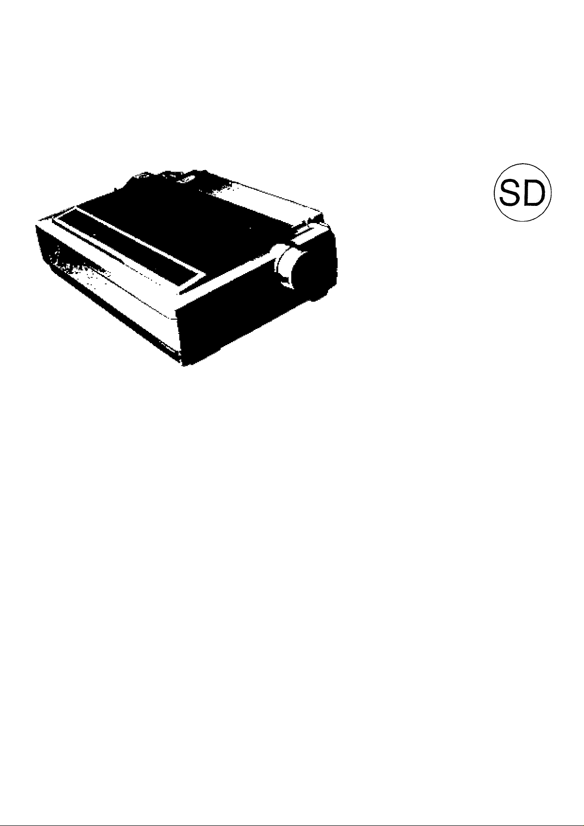
KX-P1150
Panasonic
Page 2
KX-P1150
1. Specifications
Power requirements:
Current:
Power consumption:
Interface:
Print mode:
Character sets:
Buffer: 4K (standard), additional 32K (optional KX-P44)
Dot configuration:
Character size
Normal characters:
Character per line (cpI)
(per inch (25.4mm) (cpi)):
AC220-240V, 50/60Hz
Idle: 0.1A; Maximum 0.7A
Max
------
60 W
Standby 5W
Self Test
Centronics parallel
Draft, Near Letter Quality (Courier, Bold PS, Times Roman, Sans Serif)
96 ASCII characters, 33 International characters (14 countries + LEGAL Set no
science), 158 IBM-PC special characters, 38 Multilingual characters
Dot Diameter: 1/84 inch (0.3mm)
Dot Alignment (HxV)
Dot Pitch
0.074(W) X 0.097(H) inch (1.89 x 2.46 mm)
Pica
Elite 96 cpi (12cpi) 48 cpi (6cpi)
Micron
Compressed 137 cpi (17cpi)
Elite compressed 160 cpi (20cpi) 80 cpi (lOcpi)
-----
35 W
(H)
(V)
Draft NLQ
9x9
1/120"
1/72"
Draft, LQ
80 cpi (lOcpi) 40 cpi (5cpi)
120 cpi (15cpi)
18x18
1/240"
1/144"
Elongated
60 cpi (7.5cpi)
68 cpi (8.5cpi)
Print speed:
Print direction:
New line time:
Paper feed:
Paper used:
Paper thickness:
Number of copies:
Printer emulation:
Micron
Draft
Letter Quality
Text printing: Bi-Directional
Bit Image printing: Uni-Directional & Bi-Directional
Approx. 100 msec [with 1/6 inch (4.2 mm) line feeding]
Friction and Push Tractor
Fanfold paper
Single sheet
Envelopes
Total thickness of sheets must be less than 0.013 inch (0.32 mm).
Original -(- 3 non-carbon copies
EPSON
IBM
(102-254mm1
(102-297mm)
FX-850
Proprinter 111
240 cps 192 cps
32 cps
Width
4-10 in
4-11.7 in
Standard business envelopes ie: #6, #10 size
16-24lbs.
14-24 lbs.
Elite
38 cps 32 cps
Weight
(127-363mm)
Height
5-14.3 in
Pica
160 cps
Page 3
KX-P1150
Storage environment:
Temperature: -4°F to 140°F (-20°C to + 60°C)
Humidity: 10-90%RH
Operating environment: Temperature: 50°F to 95°F (+10°C + 35°C)
Humidity: 30-80%RH
Head service life:
Approx. 200 million strokes in draft mode
Ribbon: Cassette seamless fabric ribbon
Black ribbon cassette KX-P115/KX-P115i:
Life expectancy (in Draft mode) (rolling ASCII)
Approx. 4 million characters
Optional accessories: Auto Cut Sheet Feeder (single bin) (KX-PT12)
32K Buffer Chip (KX-P44)
Ribbon Cassette (black) (KX-P115/KX-P115i)
Dimensions:
17.1" (W) X 12.4" (D) X 5.3" (H) in. (434 x 314 x 134.5 mm)
Weight: Approx. 10.6 lbs. (4.8 kg)
Printing area: Fanfold paper
J^i
_________
A
B
C 0.33" (8.38 mm)
■ 1st character
D
A; Value A indicates the area near the paper
Printing area
---------------------
i— Paper perforations
Printing area
-
To-i:
perforations where the quaiity may not be
optimum.
B
Vaiue B indicates the maximum distance
between the sprockets and first printabie
character. (When the ieft tractor is set on the
left end and the margin is set to 0.)
C: Value C indicates the area from the top edge
of the paper to the top of the first printed
character.
D: Value D indicates the position where paper out
is detected and printing may not be optimum.
Single sheets and Envelopes
B
C
D
»*
B
arc
B: Value B indicates the minimum distance
' 1 St character
Printing area
Id
between the edge of the paper and the first
printable character.
C: Value C indicates the area from the top edge
of the paper to the top of the first printed
character.
D: Value D indicates the position where paper out
is detected and printing may not be optimum.
(When printing on envelopes, do not print on
area where edges overlap. Print quality may
not be optimum.)
Fanfold Paper
1" (25.4 mm)
0.7" (17.8 mm)
1" (25.4 mm)
Single sheets and Envelopes
1.5" (38 mm)
0.33" (8.38 mm)
1" (25.4 mm)
Specifications are subject to change without notice.
Page 4
KX-P1150
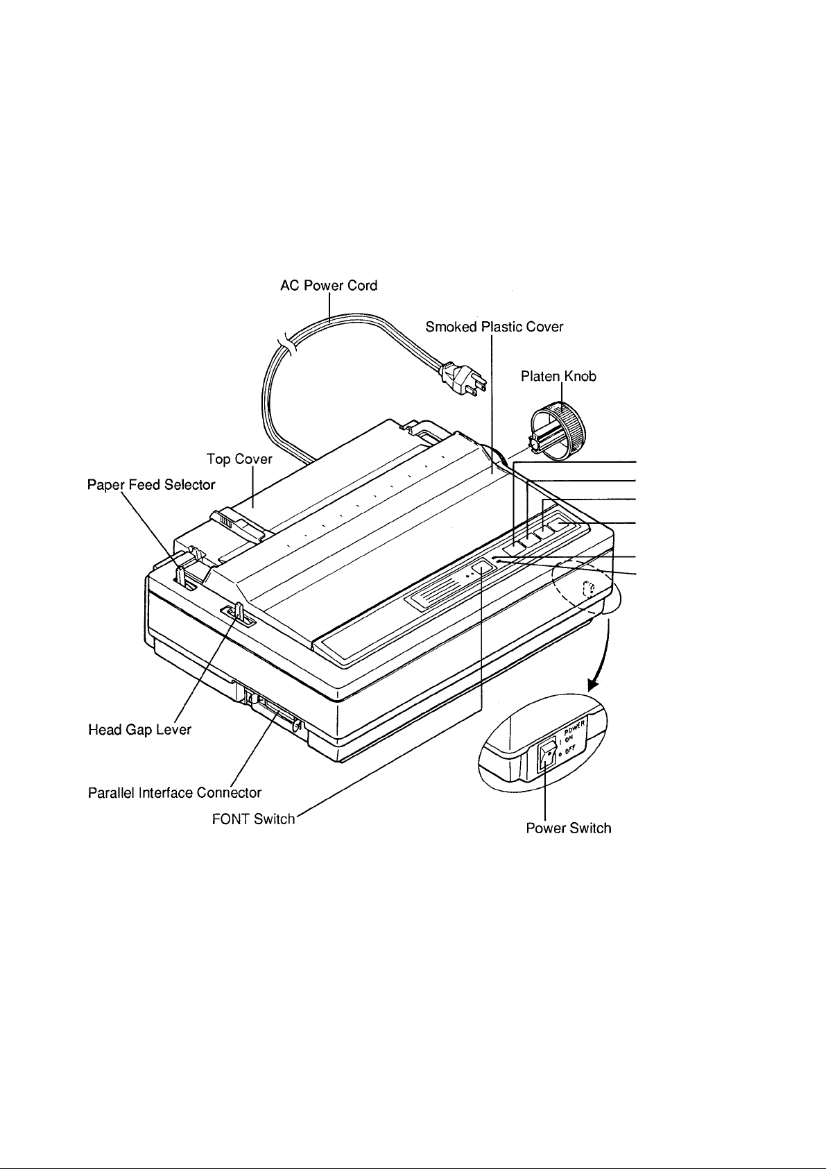
2. Operator Controls/Indicators
■ON LINE Switch
■TEAR OFF Switch
-LF/FF Switch
■LOAD PARK Switch
-ON LINE Indicator
•POWER/PAPER OUT
Indicator
Page 5

KX-PllSQ
3. Setting of Controls
This section covers the basic operation of the printer. For more detailed operation, refer to the operator's
manual.
3.1 Print Mode
®® PROGRAM
Courier
@®
®@
Rom an O O
Bold PS POWER
Sans Serif
^®"
FONT
ON LINE
o
PAP ER OUT
ON LINE
TEAR
OFF
LF/FF
LOAD
PARK
FONT switch:
ON LINE switch:
LF/FF switch:
TEAR OFF switch:
LOAD/PARK switch:
FONT indicators:
ON LINE indicator:
POWER/PAPER OUT indicator:
Pressing this switch will select the font style.
This switch opens and closes the communication line with the computer.
Pressing this switch advances the paper one line at a time. Holding this
switch advances the paper to the first print line of the next page.
Pressing this switch will advance or reverse the paper for tearing off.
Pressing this switch will load or park the paper.
These indicators identify which Font has been selected.
This indicator is lit when the printer is in the ON LINE mode and is out in the
OFF LINE mode.
This indicator is lit when the power is on and paper is installed. It blinks
when paper is not installed.
Page 6

KX-P1150
3.2 Service Operation
The following service functions can be executed when checking, adjusting or testing the printer.
Operating Switch Function Name Description
LF/FF switch + Power switch
ON LINE switch, LF/FF switch +
Power switch
ON LINE switch + Power switch
FONT switch + Power switch
TEAR OFF switch + Power switch
Self. Printing Test
Print Timing
Head Aging
Hex-Dump
Demonstration
Printing
All characters stored in the FONT ROM are printed
for 20 minutes.
When adjusting the Print Timing, use this function.
For more detailed information please refer to Section
5.2 Print Timing
After installing the new printhead, use this function to
check the movement of the printhead pins. Do not
use this function more than 30 minutes.
This function is for analyzing the data being
printed by the printer. When the function is
activated, all data received by the printer is printed
in hexadecimal code.
The printer will perform Demonstration Printing.
Note: After completing each of the above checks, turn the power switch off to reset the unit.
Page 7
KX-P1150
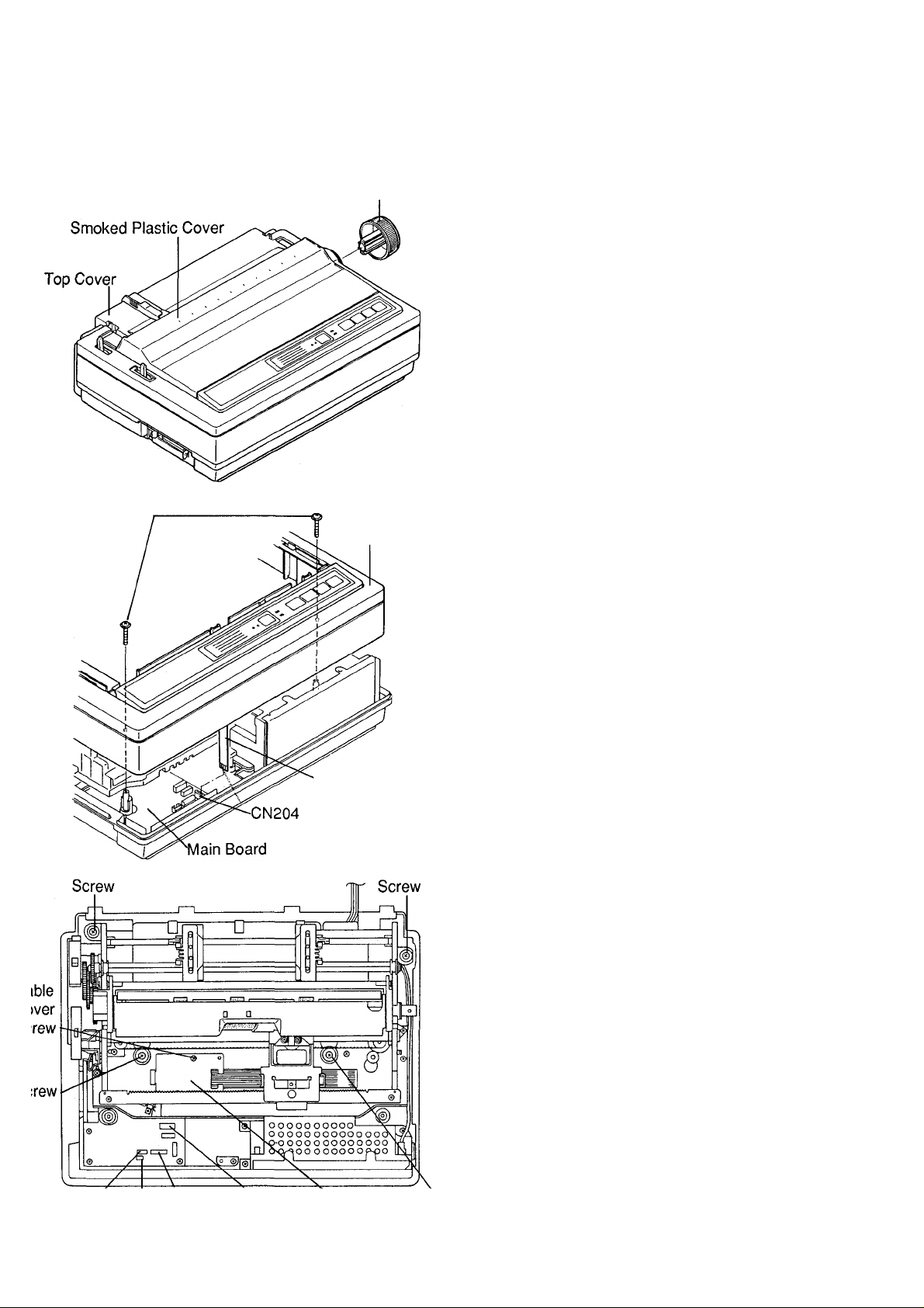
4. Removal and Replacement Procedures
For safety and to avoid possible damage to electronic components, the AC line cord must be unplugged before
disassembly.
Platen Knob
4.1 Covers
Caution: The control panel board is installed on the
upper cabinet. The control panel cable is
attached to connector CN300 on the
control panel board and connector CN204
on the main board.
When lifting off the upper cabinet from the
machine, be careful not to damage the
connectors and control panel cable.
1. Remove the paper stand and smoked plastic
cover.
Screws
2. Remove the platen knob.
Upper Cabinet
3. Remove the screws (2) from the upper cabinet.
4. Lift off the upper cabinet.
5. Unplug the control panel cable from connector
(CN204) on the main board.
6. Remove the Upper Cabinet.
Control Panel Cable
4.2 Printing Mechanism
1. Unplug connectors CN201, CN202, CN206 and
CN207.
2. Position the carriage on the right side.
CN206 CN201 CN202 Cable Cover Screw
CN207
3. Remove the cable cover screw and cover.
4. Unplug the printhead flat cable from connector
(CN203) on the main board.
5. Remove the screws (4) from the chassis.
6. Lift off the printing mechanism.
Note: Use care when removing the cable cover to
avoid damaging the print head flat cable.
Page 8
KX-P1150
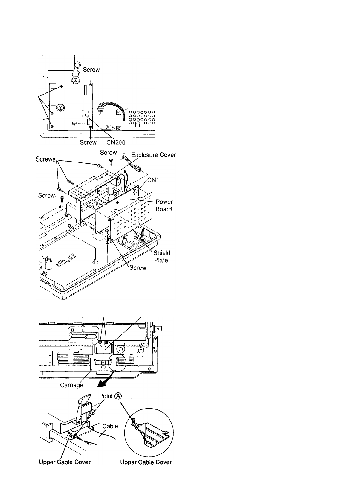
Screws
4.3 Main Board
1. Unplug connector (CN200) on Main Board.
2. Remove the screws (5) from the Main Board.
The Main Board can now be removed.
4.4 Power Board
1. Unplug connector CN1 on the power board.
2. Remove the screws (3) from the power supply
unit.
Opening Screws Printhead
3. Remove the screws (4) from the enclosure cover.
4. The enclosure cover, shield plate and power
board can now be separated.
4.5 Printhead
1. Position the carriage at the opening.
2. Remove the screws (2) from the printhead.
3. Release the upper cable cover from the carriage
by pushing down on the upper cable cover at
point (A).
4. Remove the printhead by lifting the printhead and
unplugging the printhead flat cable.
Note: When reinstalling the upper cable cover,
ensure that the print head cable is not pinched
by the cable cover latches.
Note: When the printhead is installed, ensure that
the head gap is correct.
Refer to section 5.1.
Page 9
KX-P1150
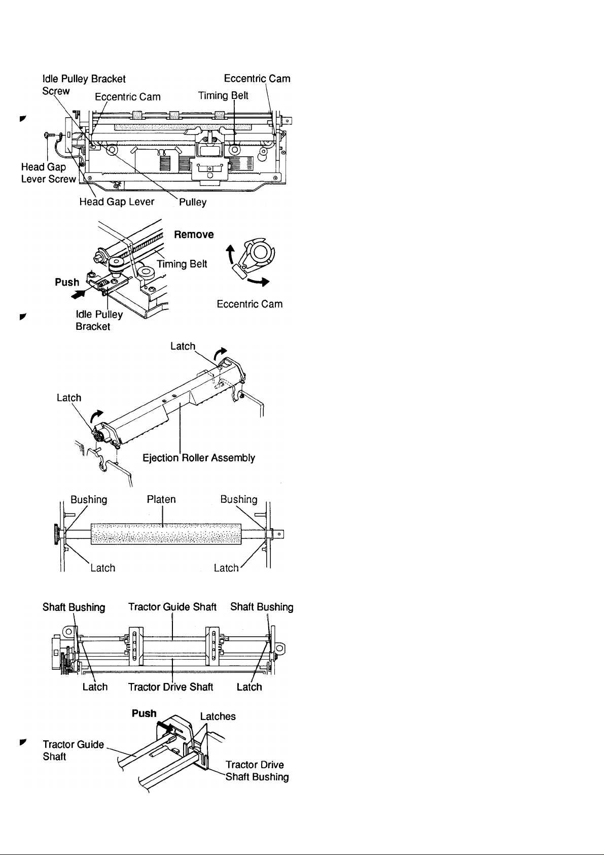
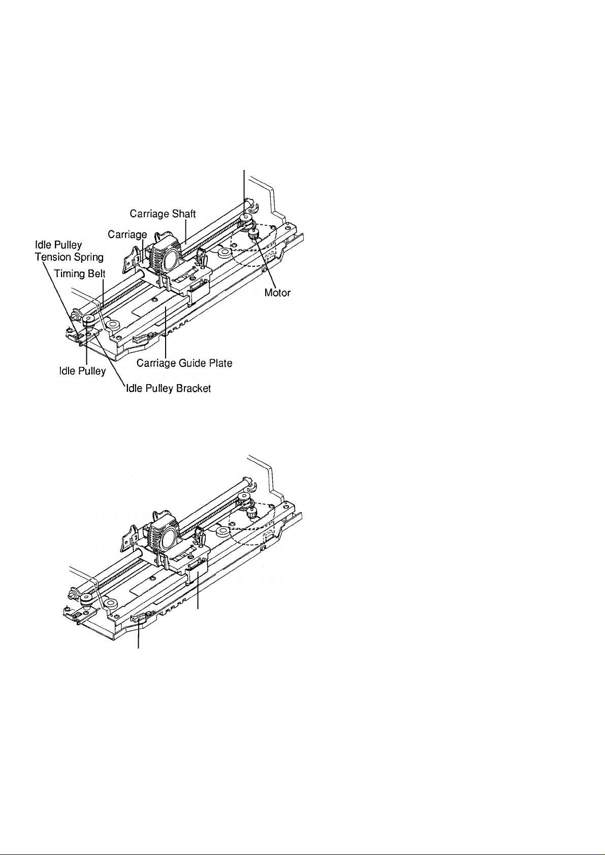
4.6 Carriage Assembly
1. Loosen the idle pulley bracket screw (1) and
release the timing belt from the pulley.
2. Remove the head gap lever screw, and Ground
Wire. Remove the head gap lever.
3. Remove the carriage shaft eccentric cams from
the right and left side frames by turning either
clockwise or counter clockwise.
4. Slide the carriage shaft out from the left side and
remove the carriage shaft.
Note: When installing the carriage assembly and its
shaft, ensure that the head gap is properly
adjusted. (Refer to section 5.1).
Tractor Drive
4.7 Platen Assembly
1. Release the latches on the ejection roller
assembly.
2. Rotate the ejection roller assembly forward.
3. Remove the ejection roller assembly by lifting
straight up.
4. Release the latch of the platen bushings from the
left and right side frame. Rotate the bushings
toward the rear of the machine.
5. Slide both platen bushings out of the frame by
pushing them inward.
6. Lift off the platen assembly.
Tractor Drive
4.8 Tractor Assembly
1. Release the tractor guide shaft from the left and
right side frame by pushing the iatches.
2. Release the latches of the left and right tractor
drive shaft bushings.
3. Lift off the tractor assembly.
Page 10
KX-P1150
5. Adjustment
(Head Gap Lever)
Ac
H
E
A
D
G
A
P
V c
+
Single
Sheet
Position
(Paper Feed Selector)
□
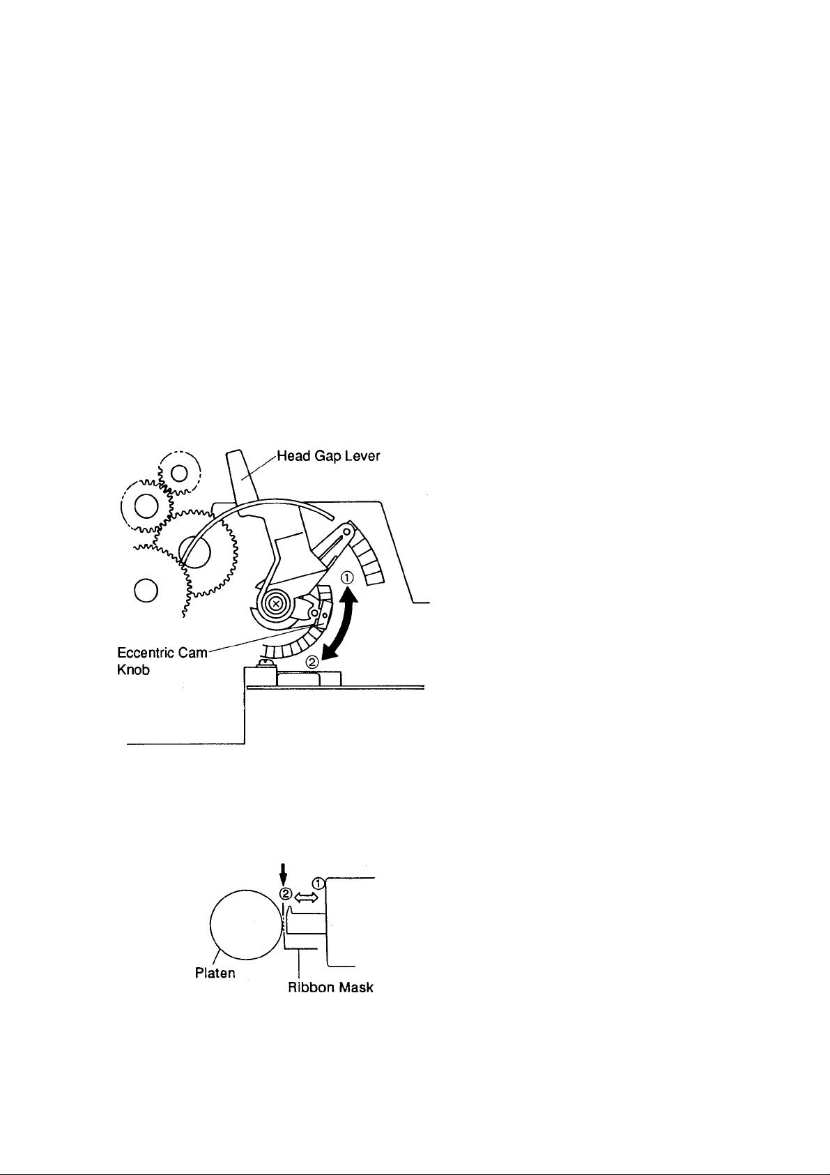
5.1 Head Gap
1. Set the head gap lever to the single sheet
position.
2. Set the paper feed selector to the position.
3. Ensure the printhead is firmly secured with 2
screws.
4. Move the carriage to the left side and adjust the
head gap between the platen and the printhead
for a clearance of 0.35mm-0.4mm by turning the
left eccentric cam.
0.45 mm Gauge^,^^ n
(does not pass)
0.40 mm Gauge\^ n
(does pass)
5. Move the carriage to the right side and adjust the
gap as per step 4 above by turning the right
eccentric cam.
Note: The projection on the eccentric cam is
released from the adjustment hole by pulling
the knob. Turning the eccentric cam one step
causes 0.037mm ± 0.052mm head movement.
Note: Use only a round wire feeler gauge of the
specified dimension for this adjustment.
Note: The head gap adjustment is required when
replacing the head, platen, carriage, carriage
shaft or eccentric cams.
Note: Moving the head gap lever towards the®
position increases the head gap clearance,
and moving toward the(2)position decreases
the clearance.
Page 11

KX-P1150
5.2 Print Timing
This adjustment is used for adjusting the print timing.
There are 6 different speeds at which the print timing
can be adjusted.
abnormal
H H H
normal
The print timing is adjusted using the following
procedure:
1. Turn on the power while holding the ON LINE
and LF/FF switches.
2. Press the FONT switch to print the "H" pattern.
The "H" pattern will be printed for 4 full lines.
3. Check the print timing comparing the "H" pattern
from line to line.
4. If the print timing is misaligned, adjust it by using
the LF/FF (Move to right) and ON LINE (Move to
left) switches and retry the printing for a final
check.
Note: Pressing the LF/FF or ON LINE switch moves
the line in 1/1440 inch increments.
5. Press the TEAR OFF switch to select the next
print speed.
6. Repeat steps 2-4 for each print speed.
7. Press the LOAD/PARK switch to save the print
timing in memory. The printer will return to the
normal print mode.
Note: If the second line of the "H" pattern is shifted
by more than half of an "H" character, be sure
the printing mechanism is normal before
starting adjustment.
Page 12
KX-P1150
6. Mechanical Function
6.1 Carriage Drive System
Carriage Drive Gear
The Carriage Drive System uses a pulse motor to
move the carriage 1/60 inch per single drive pulse.
The carriage slides on the carriage guide plate and
carriage shaft when spacing to the right and left.
6.1.1 Power Transmission Mechanism
The rotation of the carriage motor is transmitted to the
carriage through the carriage drive gear. The timing
belt fixed under the carriage is looped around the idle
pulley and carriage drive gear. This causes the
carriage to move left and right along the carriage
shaft. The timing belt is given proper tension by the
idle pulley tension spring hooked between the pulley
bracket and chassis.
Leaf Switch
Barrier Tab
6.1.2 Print Timing
Print timing for pica (1/60 inch) and elite (1/72 inch) is
generated by a software operated timer. Refer to
"Carriage Motor Drive Block" page 33.
6.1.3 Home Position Detector Mechanism
The home switch is a leaf switch located at the far left
of the printer. Its function is to notify the CPU of the
carriage reference position. During spacing operation,
when the carriage approaches the left margin, the
barrier tab, mounted under the carriage, actuates the
home switch, generating the signal and indicating
carriage position to the CPU.
Page 13
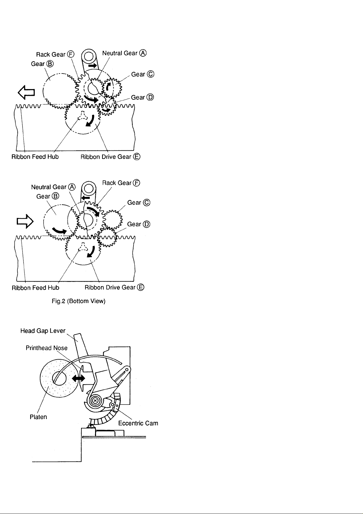
Fig,1 (Bottom View)
KX-P1150
6.1.4 Ribbon Cassette Drive Mechanism
This function performs the ribbon feed operation in
accordance with the movement of the carriage. The
ribbon cassette drive mechanism is shown in Figures
1 and 2.
This mechanism gives uniform ribbon feed
regardless of the direction of the carriage movement.
It consists of the rack gear 0 , ribbon drive gear (§)
with the ribbon feed hub and 3 gears.
When the carriage moves to the right (Fig.1), rack
gear 0 turns the neutral gear ® counter-clockwise.
The neutral gear 0 then engages with gear ® via
the gear (5) which turns the ribbon drive gear 0
clockwise with the hub.
When the carriage moves to the left (Fig.2), rack
gear 0 turns neutral gear @ clockwise. Neutral
gear ® then engages with gear 0 which turns
ribbon drive gear 0 clockwise with the hub.
6.2 Paper Thickness Selection
Selection for the number of copies is made by
changing the distance between the platen and the
printhead nose tip. When the head gap lever is
operated, the carriage shaft revolves on the
eccentric cams, moving the carriage forward or
backward.
Page 14
KX-P1150
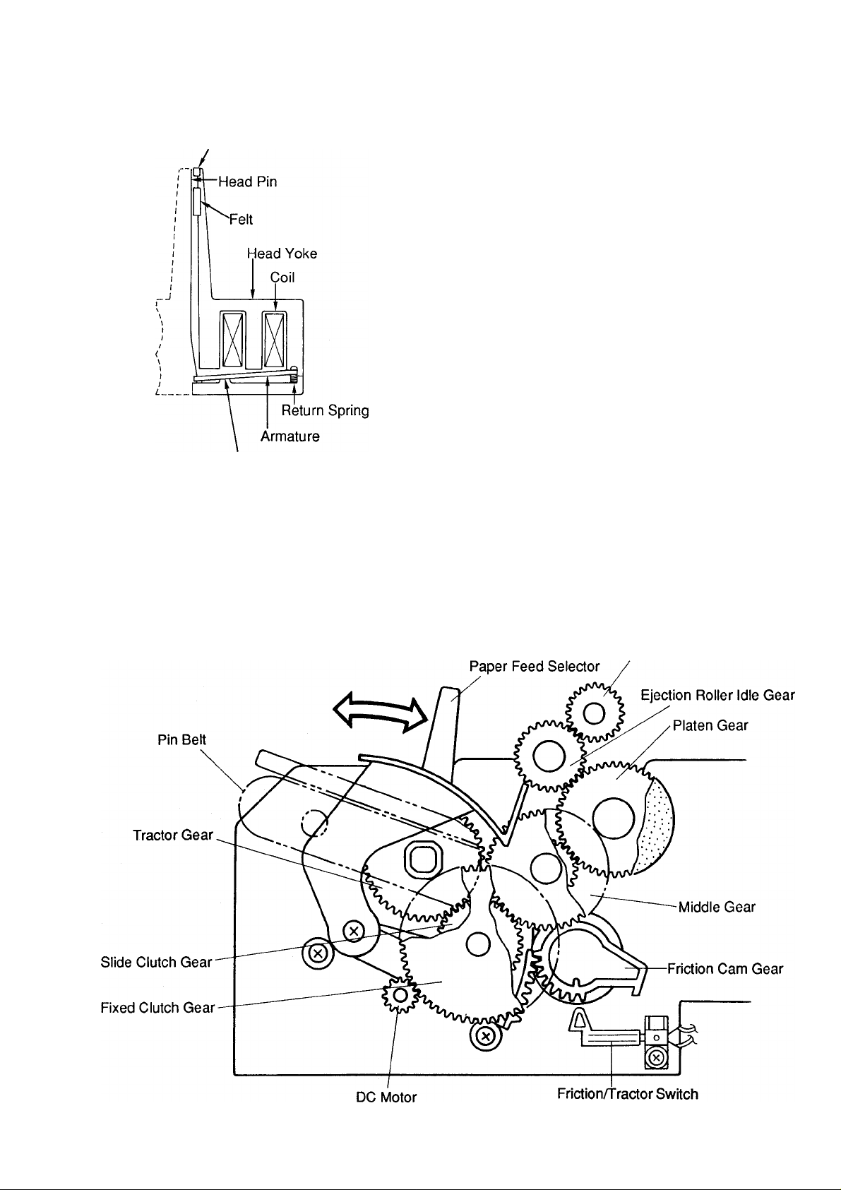
6.3 Printhead
Pin Guide
Stopper
6.4 Paper Feed Mechanism
The printhead utilizes 9 electromagnets as a driving
source, which causes the pins to strike the ink ribbon
against the platen and onto the typing paper for
matrix printing. The construction of the printhead is
shown at the left.
6.3.1 Power Transmission Mechanism
The set of 9 electromagnets consists of a one piece
yoke and 9 coils. The armature which secures the
pins is supported by this yoke.
6.3.2 Printhead Pin Operation
When the coil assembly is excited by a print signal,
the armature is drawn in, and the pin secured by the
armature is guided by the various guides to move in
the direction of the platen. The pin strikes the ribbon
to the paper. Next, the return spring moves the
armature and pin from the platen back to the rest
position.
A DC pulse motor is used as a paper feed motot. Both continuous paper and single sheet can be fed by
operating the paper feed selector. Continuous paper is loaded on both left and right sides of the pin belt on the
tractor drive device. Continuous paper is fed from the rear of the printer. Single sheet is fed from the top of the
printer. The paper feed mechanism is shown below.
Ejection Roller Gear
Page 15
KX-P1150
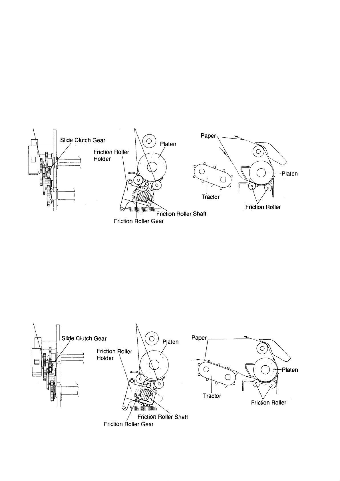
6.4.1 Friction Paper Feed Mode
This mode is for feeding single sheet paper from the top of the printer in the friction paper feed position. By
operating the paper feed selector, the fixed Clutch Gear is disengaged from the Slide Clutch Gear. As a result,
the Tractor Gear is released from its power transmission mechanism.
When setting the paper feed selector at single sheet paper position, the Friction Roller Gear rotates in a
clockwise direction. As a result, the Friction Roller Shaft revolves, allowing the Friction Rollers to contact the
platen for gripping the paper when feeding. The Friction Roller Gear also pushes the leaf switch to notify the
CPU that the selector is in the" Q " Friction position.
Fixed Clutch Gear
6.4.2 Tractor Paper Feed Mode
This mode is for feeding continuous paper from the rear of the printer. By moving the paper feed selector to the
" ini" Tractor position, the Slide Clutch Gear is engaged with the Fixed Clutch Gear. This enables turning of the
tractor drive mechanism for push mode. When the paper feed selector moves to the" 0" Tractor position the
Friction Roller Gear is rotated in a counterclockwise direction. As a result, the Friction Roller Shaft revolves and
moves the Friction Rollers away from the platen. This enables free paper passage from the rear of the
machine. The Friction Roller Gear also breaks contact with the leaf switch to notify the CPU that the selector is
in the" p]" Tractor position.
Friction Roller
Fixed Clutch Gear
Friction Roller
Page 16
KX-P1150
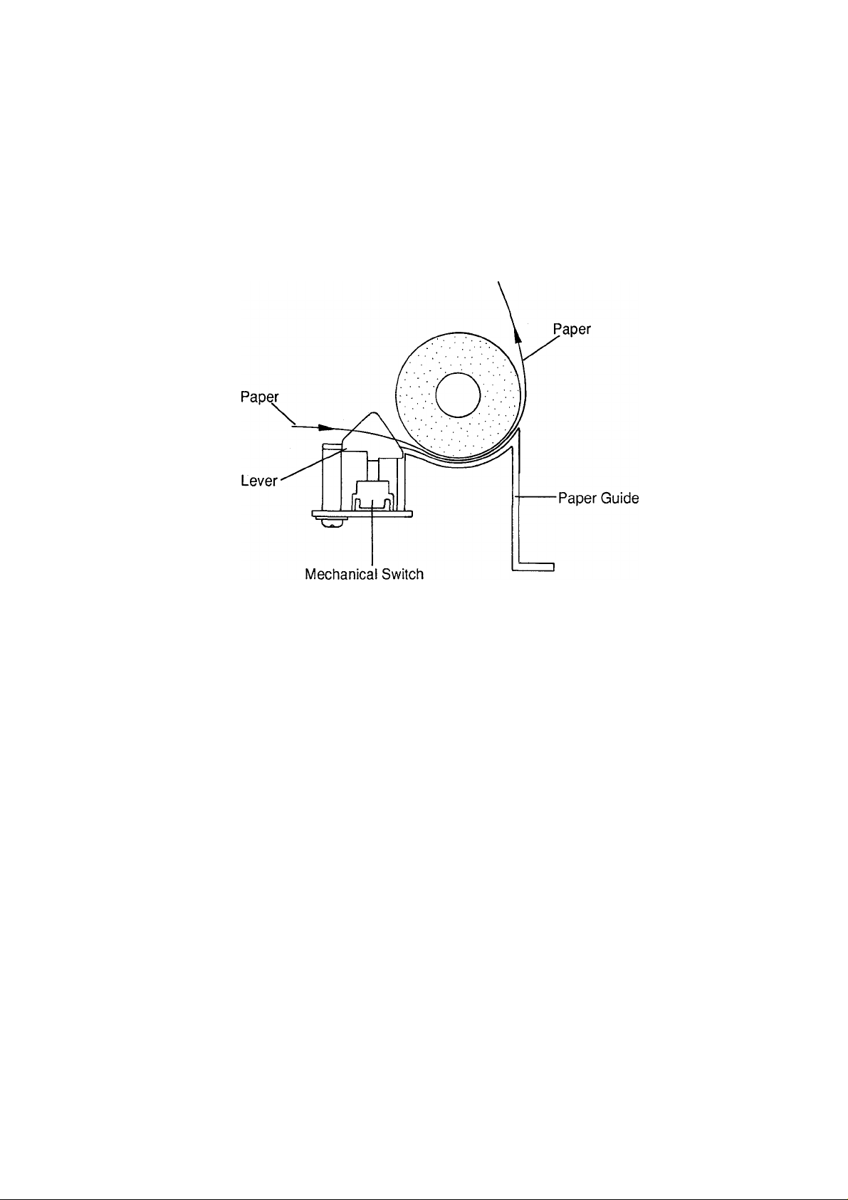
6.5 End of Paper Detector
The printer uses a mechanical switch for detecting paper out with continuous or single sheet paper. When
paper is loaded In the printer, the lever is down, and the condition of the mechanical switch is on. This sends a
signal to the CPU indicating paper loaded in the printer. When paper is out, the lever is up, and the condition of
the mechanical switch is off. This removes the signai from the CPU indicating no paper is in the printer.
Page 17

тз
g
Page 18

KX-P1150
8. Electronic Circuit Descriptions
8.1 Principle of Operation
The KX-P1150 has three Micro switches. The home position switch sets a reference for the carriage and is
necessary for aligning the first print position. The Friction/Tractor switch detects the selected method of
paperfeed (Friction or Tractor).
The paper out switch detects paper end and prevents printing when the printer is out of paper.
The printer has three drive circuits: carriage spacing motor, paper feed motor and printhead.
The control panel is composed of switches and LEDs that indicate the various states of the printer.
Logic Diagram
Printer
Page 19

8.2 Circuitry
8.2.1 Power Supply Block
(1) Block Diagram and Schematic Diagram
KX-P1150
l-J
C-D VOLTAGE WAVE E-F VOLTAGE WAVE
Ml
w
Page 20

KX-P1150
(2) Description
(a)
Input Circuit
This circuit decreases RF and eliminates transient line noise. After the AC line voltage is filtered, it is
supplied to the rectifier circuit. Fuse F001 protects the power supply from external power surges and
internal current overloads.
C006
(b) Rectifier Circuit
The AC power is rectified by D001, then supplied to the converter circuit and provides the Kick-on
voltage for control circuit (MC001) through R008-R013. Over current protection in this circuit is
provided by TH001.
Page 21

(c) Converter Circuit
This power supply produces 2 output voltages (+36VDC and +5VDC). The output voltages are stabilized
by controlling the on and off period of Transformer T001, which is controlled by MC001 monitoring the
+36VDC output and then turning Q001 on and off. +8VDC is input to IC101, a three pin regulator that
regulates the +5VDC output.
KX-P1150
+36V
GND
+ BV
(d) Control Circuit and Error Detection Circuit
When the +36VDC output voltage increases, the current of photocoupler PC001 increases, MC001
monitors this current level and controls on and off time of Q001. The turning on and off of Q001 controls
the oscillation frequency of T001 which regulates the +36VDC output.
(e) Over Current Limiter
IC101 has built in over current protection and protects the +5VDC circuit from current overload. Control
circuit MC001 provides over current protection for the +36VDC circuit by controlling Q001 turn on time
by an internal limiter circuit.
Page 22

KX-P1150
8.2.2 CPU and Peripheral Circuit Block
(1) This block diagram consists of the CPU (IC200), Gate Array (IC205), ROM (IC202), RAM (IC203) and
optional RAM (IC204). It receives the data from the host computer, processes the input from the printhead
overheat sensor and operation switches, and controls the carriage, paper feed motors, and the printhead.
ROM contains the operation program, which controls data processing and mechanical functions and the
character generator, which determines the appearance of the characters.
IC202 IC203 IC204
Page 23

(2) CPU Functions
Block Diagram
KX-P1150
(b) Timer / Counter
(16bitx2, 8bitx4)
(c) A / D Converter
(a) CPU
This block mainly consists of the Program Counter, Arithmetic Logical Unit, and Instruction Decoder. This
block fetches the program from the ROM, decodes the instructions, and processes it accordingly.
(b) Timer/Counter
This block consists of two 16-bit timers and four 8-bit timers. They are used for generating the timing for
the printhead and carriage motor.
(c) A/D Converter
In this circuit, 8 bits/4 channel A/D Converters are prepared. One channel is used for sensing the overheat
of the printhead and other channels are used for sensing the input of control panel switches.
(d) Watch Dog Timer
(e) I/O PORTS
(d) Watch Dog Timer
When a program does not run properly, the CPU is reset.
(e) I/O PORTS
These ports are used for sensing the input of Paper End, Friction/Tractor, Home switches and driving the
LEDs in the control panel.
Page 24

K5C-P1150
(3) CPU Pin Functions
The CPU has total of 64 pins and an 12MHz clock. It controls a 128KB ROM, 8KB RAM and 32KB optional
RAM. These RAMs are used as an input buffer, line buffer, bit image buffer, and download area. The CPU
pin functions are as follows.
CPU
12MHz Clock
IC205 Addressing
Address Bus
Address/Data Bus
Address Latch -------------
3.7 MHz
HTRG
CRTRG**
Interrupt 0
Interrupt 2
-----------
-------------
-------------
--------------
------------
------------
-----------
OSC (XI ,2)
►
l/OCS (A22)
A8-A19
AD0-AD7
ALE
CLK ANO
T04
T01
INTO
►
INT2
P31-P34
AN2
AN3
AN1
P70-P73
Reset
RD
WR
•*
----------
-----------
-----------
-----------
^
-----------
-----------
EEPROM DI/0
Head Temprature
FONT, LF/FF
TEAR OFF, LOAD PARK
ON LINE
LEDs
Reset
► OE (for ROM, RAM, GA)
-► WR
Page 25

(4) Gate Array
The gate array (IC205) is a 100 pin Flat Package, which consists of seven blocks.
(a) Head Drive Controller
The 9 Print Head Pins are controlled by a Head pin group controller. The Head Pin Trigger Pulse
triggers generation of the Head Pin Signal from each group.
(b) Decoder
It is used for accessing ROM and RAMs, and used for refreshing RAMs.
(c) Handshake Interface
In this gate array, the Centronics Parallel Interface (usually called Handshake Interface) is prepared.
The busy signal to the host computer is generated automatically when receiving the DSTB (data
strobe) signal. The ACK (acknowledge) signal is also generated automatically when the busy signal
turns to L level (Ready state).
(d) Pulse Generator for Stepper Motor
In this gate array the pulse generator for the stepper motor is prepared. This function is used for the
carriage spacing motor and line feed motor. The motor driving pattern is generated automatically
when the generator receives the starting signal. This pattern is synchronized with the output of the
timer which determines motor pulse rate.
KX-P1150
Page 26

KX-P1150
(5) Gate Array Pin Function
The pin functions are as follows.
CPU
lOCSi
A19
GATE ARRAY
Address
Head Pin Data (Sink Tr)
MEMORY
CPU
CPU
IC202^
IC203^
IC204^
LF Motor Enable
LF Motor Phase
A15
A7
AO J
AD7n
ADO
RESET
ALE
CLK
RD
WR
CRTRG
HTRG
ROM1
RAM1
RAM2
LFEN
LFA
LFNA
LFB
LFNB
Address
Address/Data
H9
HTD
INTO
INT2
HSO
HS7
STB
ACK
BUSY
PE
ERROR
SELECT
AFXT
PRIME
CRA
CRNA
CRB
CRNB
CRCNTO
CRCNT1
CRCNT2
-► Head Pin Data
(Common Tr)
Carriage
Counter,
PRIME
-►STB
Parallel Data
— Strobe
-► Acknowledge
Busy
-► Paper End
-► Error
-*■
Select
— Auto Feed XT
— Prime
CR Motor Phase
CR Motor
Power
Control
to CPU
Interrupt
output
Page 27

KX-P1150
8.2.3 Parallel Interface Circuit
The Interface Block receives data from the host computer and generates the appropriate status signals.
The handshake method is described in the following steps.
Process
(1) A STROBE signal is sent from the host computer and is used to set the internal latch of the Gate Array. At
the same time Gate Array pin (3) sends a BUSY signal to the host computer.
(2) The CPU checks the internal latch of the Gate Array periodically and checks whether a STROBE is sent or
not
_______
(3) If a STROBE signal has been sent, the CPU reads the data through HS ports (HS0-HS7) of the Gate Array.
(4) When the BUSY signal disappears, an ACK (Acknowledge) signal is sent to the host computer
automatically during the time determined by software.
(5) The CPU then determines from the received data as to wheter it is a character code, control code or bit
image data and processes the data accordingly.
(6) The CPU processes another command (for instance: operation swtich state check, motor drive during
print).
_______
Thus the data received by handshake is accomplished.
Timing Chart
Data 1-8 from HOST —
STROBE from HOST
BUSY to HOST (pin (1^ )
ACK to HOST (pin ^ )
CN205
-T5V
EXPRM O-
R1NF0 OR1NF2 O
AFXT/1 a
PRIME0STROBE
ERROR a
SELECT
P.E. O-
ACK O-
BUSY
OATAB a
DATA? ODATAS O
DATAS a
DATA4 a
DATAS
DATA20DATAI
GND
FG
0
O-
0
0
0
0
0
0
-
-
-
«
Printer HOST
Handshake
r
j
IC20S
AFXT
PRIME
STB
ERROR
SELECT
PE
ACK
BUSY
Hb /
HS6
HS5
HS4
HS3
HS2
HS1
HS0
GATE
ARRAY
RA205
Page 28

KX-P1150
8.2.4 Carriage Motor Drive Biock
The Carriage motor is driven by the four signals from CRA, CRB, CRNA and CRNB, and is driven by 1-2 phase
driving system.
The time interval is determined by the CPU's interval counter clock as generated from the CPU's clock.
This circuit is a chopper drive circuit for fixing the amount of the current through the motor during stepping and
has two threshold voltages
proportion to the current through the motor. For example, when the voltage drop across R212 (R213) is larger
than
Vsh,
IC207 is turned off and Q202 (Q203) is turned off, then Q200 (Q201) is turned off. At the same time, the
current through the motor decreases, because the voltage drop across R212 (R213) decreases. When this
voltage drop is smaller than
The amount of current through the motor is fixed during stepping by repeating this process.
(Vsh, Vsl).
Vsl,
IC207 is turned on, and the current through the motor increases.
IC207 compares the voltage drop across R212 (R213) which is in
These threshold voltage
(Vsh, Vsl)
are able to be changed by IC205
pin
95 H or L signal duty Ratio according to
Timing Chart
CRA
CRB
CRNA
CRNB
Carriage Motor Coil Resistance Value
Pin No.
(CN202)
6-5
4-5
1-2
3-2
Resistance Value
9.5 ± 0.7 ohms
9.5 ± 0.7 ohms
9.5 ± 0.7 ohms
9.5 ± 0.7 ohms
Page 29

Pulse Rate Chart
Relation between the printing mode and the pulse rate is shown in the chart.
Printing Mode
Holdinq State 0
10CPI
DRAFT
LQ
12CPI
15CPI
17CPI
20CPI
10CPI
12CPI
15CPI
17CPI
20CPI
Pulse Rate(PPS)
1953
1953
1953
977
977
977
977 6/128
651 6/128
488
488
Current Control
CRCNTO OUTPUT PULSE DUTY
20/128
10/128
10/128
10/128
6/128
6/128
6/128
6/128
6/128
Note: The CRCNTO Output Pulse Duty Cycle is determined by dividing the on time
of the pulse (b) by the total time of the pulse (a), measured at point A of the
carriage motor drive circuit.
b/a=CRCNTO Output Pulse Duty Cycle
8.2.5 Paper Feed Motor Drive Block
KX-P1150
POINT A
b
During paper feed, IC205 sets LFEN (pin @ ) at the H level and turns on Q204 and 0205. +39V is then fed to
the motor.
The driving method by LFA, LFNA, LFB, LFNB is a 2-2 driving system and the pulse rate is 400 pulses per
second. When paper feed is not active, 0205 is turned off by LFEN (pin @) L level signal and then a holding
voltage (about 2V) is applied to the motor through R214.
The Line Feed Motor is protected from current overload by setting LFA, LFNA, LFB, LFNB and LFEN to a L
level. This is controlled by the Dip-SW Port of IC205 (pin @ ) detecting the collector voltage of 0205 through
R221-R223 and R260.
Timing Chart
R222 R221 R260
Paper Feed Motor
LFA _
LFB
LFNA
LFNB
Pin No.
(CN203)
1-2
3-2
4-5
6-5
Resistance Value
140 ± 10 ohms
140 ± 10 ohms
140 ± 10 ohms
140 ± 10 ohms
Page 30

KX-P1150
8.2.6 Head Drive Block
This block consists of Q208-216 and Q206, Q207. Q208-216 control each pin and Q206, Q207 control the
power supplied to the printhead.
The CPU (IC200) sends the printhead trigger pulses from terminal T04 to the Gate Array. During this time, the
head pin solenoids are fired by Q206-216 according to the data received from the Gate Array as H1-H9. IC205
and Q206, Q207 control the current used to drive the pin solenoids. A thermistor is attached in the printhead
and is used to detect overheating.
Timing Chart
Print Data ^
Trigger Pulse
Print Pulse
Print Pulse Time
Print Mode Td
Draft
Bit Image
about 280 |i sec
about 280 sec
Tp
about 492 p. sec
about 492 ц sec
X
Printhead
Pin No.
CN203
1-5
2-5
3-5
4-5
9-7.8
11-7.8
13-7.8
14-7.8
15-7.8
10-12
6
Resistance Value
24.9 ± 0.5 ohms
24.9 ± 0.5 ohms
24.9 ± 0.5 ohms
24.9 ± 0.5 ohms
24.9 ± 0.5 ohms
24.9 ± 0.5 ohms
24.9 ±0.5 ohms
24.9 ± 0.5 ohms
24.9 ± 0.5 ohms
Less than
37K±8 Kohms (at25t:)
OPEN
Page 31

о
сЗ
с
ш
(О
S
3
Л
ф
tu
о.
о
<■
ф
X
•о
Page 32

KX-P1150
8.2.7 Switch Circuits
(1) The purpose of the home position switch is to move the carriage to a reference position (home position) at
the left end of the carriage when the power switch is turned on or when a Reset signal is generated.
When the carriage comes to the home position, P60 (pin @ ) changes from H to L level.
(2) The paper out switch detects if the paper is in or out of the machine. When this switch detects paper out,
P63 (pin @ ) changes from H to L and the Power/Paper Out LED flashes to indicate paper out status.
(3) The paper feed selector switch detects if the paper feed selector is in the friction or tractor position.
If the paper feed selector switch is set to the friction position, P61 (pin @ ) is L and if set to the tractor
position, P61 (pin @ ) is H.
Page 33

8.2.8 Control Panel
The control panel is composed of 5 switches and 4 LEDs.
(1) The ON LINE switch, switches between on-line and off-line and is input to IC200 (pin @). This switch is
also used to change the current setting in the initial setup mode.
(2) The LF/FF switch is for one-line or one page-feed paper feed and is input to IC200 (pin @)).
(3) The Font switch selects the character fonts and is input to the CPU (pin @ ). This switch is also used to
select the item in the initial setup mode.
(4) The TEAR OFF switch enables paper feeding to the tear off position and is input to the CPU (pin @ ).
(5) The LOAD PARK switch enables automatic loading and feeding back of the fanfold paper and is input to
the CPU (pin @ ).
(6) The power/paper out LED lights when power is turned on and blinks when paper out is detected.
(7) The ON LINE LED lights when at the on-line status.
KX-P1150
(8) Two Font LEDs display Font Type.
IC200
CPU
P70 (Ml 01
(Mil)
P71
P72 (Ml 2)
P73 (M13)
AN0
AN1
AN3
R245.
Tw:
R247'
RA214.-:^
b
U
CN204
L
JT
0302 R303
----Nt----
D300 FONT
—nr-
0301
D303 POWER R302
E
8
7
l
3
7
S
1
ON LINE
V
CN500
L
X“
^
R300
-V*i—
R301
-w»—
'8300
, nS)q301
----
,, Vd^Q302
FONT
f—O O—-I
SW300
TEAR
OFF
p-O
SW302
LF/FF
rC O—J
SV303
LOAD
PARK0NLINE
-O 0—1
SW304
Page 34

KX-P1150
8.2.9 Reset, EEP ROM
(1) Reset Circuit
The reset circuit is provided to initialize the gate array (IC205) and CPU (IC200). Approximately 8msec after the
voltage at IC206 pin(D reaches approximately 4.3V, the reset terminal RES (pin0) changes from L to H.
IC206 PIN ®
IC206 PIN ©
5V
4.3V
GND
5V
GND
Power ON
--------
-------
Power OFF
8 msec
IC20B
(2) EEP ROM
This IC memorizes the setting such as printer mode character set, etc.
IC200
Page 35

8.2.10 Logic Board Connection Diagram
KX-P1150
Page 36

KX-Ptt50
8.3 Explanation of Connectors
8.3.1 Name of Connectors
Connector applications are shown below. For details, refer to
CN1
CN2
CN200
CN201
CN202
CN203
: AC Power Supply
: Power Supply (+36V,+5V,GND)
: Power Supply (+36V,+5V,GND)
: Paper Feed Motor
: Carriage Motor
: Printhead
CN204
CN205
CN206 : Friction/Tractor Switch,
CN207 : Home Switch
CN300
8.3.2 Pin Assignment
CN1 (AC Power Supply)
Pin
Signal
No.
Name
AC
1
2
AC
CN2 ,CN200 (Power Supply +36V,+5V,GND)
Pin
No,
v-rtNiiuo [ rriouüM/1 raulur owiiori.raper uui owiicri;
Pin
No.
CN207 (Home Switch)
Pin
No.
CN201 (Paper Feed Motor)
Pin
No.
Signal
Name
1
DC +36V
2
DC +36V
GND
3
GND
4
5 DC +5V
Signal
Name
1
2
3
4
1 SW
2
1
2
3
4
5
6
SW Paper Out Switch
SG Signal Ground
SW
SG Signal Ground
Signal
Name
SG
,
Signal
Name
LFA Line Feed Motor Phase A
SLF
LFNA
LFB
SLF
LFNB
AC 220-240V —
AC 220-240V
For Printhead,Motor
For Printhead,Motor
Ground
Ground
For Main Board Logic Circuit —
Friction/Tractor Switch
Home Switch
Signal Ground
Line Feed Motor Power Supply
Line Feed Motor Phase A
Line Feed Motor Phase B
Line Feed Motor Power Supply Out
Line Feed Motor Phase B In
Description
Description
Description
Description
Description
In/
Out
— 2 SCR
In/
Out
— 6 CRA
—
—
In/
Out
In
Out 6 24
In
Out
In/
Out
In
Out
In/
Out
In
Out
In
In
CN205 (Centronics I/O)
—
tables.
: Control Panel (LED, KEY)
: Centronics I/O
Paper Out Switch
: Control Panel
CN202 (Carriage Motor)
Pin
Signal
No.
Name
1 CRB
3 CRB
4 CRA
5 SCR
Pin
Return Side
No.
19-30
Pin No.
1
2 20
3 21 DATA2
4 22 DATA3
5 23
7 25
8 26
9
10 28 ACk
11 29 BUSY
12
13
14
15
16
17
18 +5V
31
32 ERROR
33
34
35
36
19 STB
27 DATA8
30
Carriage Motor Phase B
Carriage Motor Power Supply
Carriage Motor Phase B
Carriage Motor Phase A
Carriage Motor Power Supply
Carriage Motor Phase A
Signal
Name
DATAI Handshake Data 1
DATA4
DATA5 Handshake Data 5
DATA6
DATA7
PE
SLCT
AFXT/1
SG Signal Ground
FG
PRIME Prime
SG Signal Ground
SG Signal Ground
Description
Description
Strobe
Handshake Data 2
Handshake Data 3
Handshake Data 4
Handshake Data 6
Handshake Data 7 In
Handshake Data 8
Acknowledge
Busy
Paper End
Select
Auto Feed XT
Frame Ground
+5V
Error
In/
Out
In
Out
In
In
Out
In
In/
Out
In
In
In
In
In
In
In
In
Out
Out
Out
Out
In
—
—
—
Out
In
Out
—
—
—
—
—
Page 37

KX-P1150
CN203 (Print Head)
Pin
Signal
No.
Name
1 H6
2 H4
3 H8
H2 Head Pin 2 Drive Out
4
5 COMMON
6
NC Not Used
COMMON
7
COMMON
8
H9
9
10 PTH
11
12 PTH
13
14 HI Head Pin 1 Drive Out
15 H3 Head Pin 3 Drive Out
H7 Head Pin 7 Drive Out
H5 Head Pin 5 Drive Out
Head Pin 6 Drive Out
Head Pin 4 Drive Out
Head Pin 8 Drive Out
H2. H4, H6, H8 Out
HI, H3, H5, H7, H9
HI, H3, H5, H7, H9
Head Pin 9 Drive
Connected to Signal Ground
Connected to Signal Detect
Description
In/
Out
—
Out
Out
Out
Out
In
CN204, CN300 (LED, Switches)
Pin
Signal
No.
Name
1 SG Signal Ground Out
LED
2
LED
3
LED
4
LED
5
6 SW On Line Switch In
SW
7
8 SW
9 +5V +5V Out
Font Out
Font
Power Out
ON LINE Out
Font, Tear Off Switches
LF/FF, Load Park Switches
Description
In/
Out
Out
In
In
Page 38

KX-P1150
8.4 IC Pin Configuration
8.4.1 Logic Symbol Chart
Positiva Logic
NOT
!-[>-(
BUFFER
A-l C
AND
so-
8.4.2 Pin Configuration
S5i!~::°8So8^
FK2SSSSS2SJ;]
v-OCOCSJv-OOC>J»-Qf/>rr.-v^«’'^COCVIv-
'4-Trr»r>.r'.h»LDy3<DSU)£Cl«jT-v-»-t-,-
a.Q.0.a.Q.CL0.Q.Q.Q.CCSCCO4S<<<<
C = A
C = A
C-AB
Negative Logic
A^[^C
INVERT-NOR
C = A + B
C = A
C = A
Truth Table
A
c
L H
H
L
A
C
L
L
H
H
A
B C
L L L
L H
H
L L
H H H
L
Positive Logic
NANO
OR
A
B
O-
NOR
Si><
Negativa Logic
INVERT-OR
SO-
c = XB C = *+B
INVERT-NAND
A
B
i>=
C = A + B
INVERT-AND
c=>rrB
Truth Table
c=/fS
C = A6
IC200 CPU
TMP90C845F
□ AIO
A8
X2
□ XI
3 Vss(GND)
D ALE
□ AD7
□ AD6
A04
□ AD3
PJVIGP0901
Page 39

KX-P115Q
NC [T
A16 [T
A15 [T
A12 [T
A7 [X
A6 nr
A5 [T
A4 [T
A3 [T
A2 Qo
A1 QT
AO 01
DO 01
D1 Ol
D2 01
GND fiS
IC202 Mask ROM
■V^
1Mbit
HI VDD
H] NC
30] NC
29l A14
28l A13
2T| A8
HI A9
m A11
24] OE
m A10
22) CE
m D7
H] D6
OH D5
Tsl D4
TtI D3
VPP [T
A16 HE
A15 [F
A12 [T
A7 CE
A6 CE
AS [T
A4
CE
A3 [E
A2 01
A1 QT
AO OE
DO Ol
D1 Ol
D2 Ol
GND nr
IC202 ROM
1M bit (D27C010«150)
32] VDD
3i1 PGM
30l NC
m A14
28l A13
2t1 A8
26] A9
25] A11
24l OE
HI A10
22l CE
iO D7
20] D6
IFI D5
Ts] D4
V7l D3
AU [T
A12 [F
A7
CE
A6 E
AS E
A4 E
A3
E
A2
E
A1 E
AO E
DO E
D1 E
D2 E
GND E
IC204 RAM (Option)
(TC51832)
in VDD
27l RAW
in A13
25] A8
24l A9
in A11
m OE/RFSH
in A10
in cE
El D7
E D6
E DS
E DA
E D3
A 4
A-
A+“
GND (V)
(S8054HN)
■E
-E
-E
E
IC207
(LM393)
3^
3-
v+
’ B
• B-
■ B+
NC
E
A12
E
A7
E
A6
E E
AS
E
A4
E
A3
E
A2
E
A1
E E
AO
E
DO
E E
D1
E
D2
E
GND
E
IC203 RAM
(LC3664)
E
VDD
17 ]
WE
26] VCC
A8
E
A9
E
E
OE/R^
E
A10
CE
E
D7
D6
17 1 D5
E
04
E
D3
Page 40

KX-P1150
7
V
Printhead Driver
BCE
Q208-216
(2SD2170)
12
QA201
(MP4303)
QA200
(STA471A)
Paper Feed Motor Driver
Line Feed Motor Driver
Memory Array
64x16
^
___
Address
Decoder
Vcc
GND
8 Pin SOP
Top View
IC201
(S2914AIF)
Dl -
CS .
SK-
I
Data Register
^ Mode Decode
* Logic
^ Clock Generator
BLOCK DIAGRAM Of IC201
Output Buffer
-» DO
Page 41

8.4.3 Pin Assignment
IC200 CPU (TMP90C845F)
Pin
Symbol
No.
1 P30
2 P31
P32
3
4 P33
5 P34
6 RXD
Not Used
EEPROM DATA OUT
EEPROM DATA IN
EEPROM Clock
EEPROM Chip Select
Not Used
7 P36 Not Used —
8 TXD
9 A16
A17 Address Bus 17
10
11 A18
12 A19
13 A20
14 A21
15 IOCS
16 WAIT
17 ADO
18 ADI
19 AD2
20 AD3
AD4 Address Bus 4
21
22 AD5
23 AD6
24 AD7
25 ALE
Not Used
Address Bus 16
Address Bus 18 Out
Address Bus 19 Out
Not Used
Not Used
G.A. Chip Select
No Wait In
Address Bus 0
Address Bus 1
Address Bus 2 In/Out
Address Bus 3 In/Out
Address Bus 5 In/Out
Address Bus 6 In/Out
Address Bus 7 In/Out
Address Latch Enable Out
26 GND GND
27 XI OSC In
28 X2 OSC Out
29 EA
30 A8
A9
31
32 A10
Extend Address (GND) In
Address Bus 8 Out
Address Bus 9 Out
Address Bus 10 Out
Function
In/
Out
—
Out
in
Out
Out
—
—
Out
Out
—
—
Out
In/Out
In/Out
In/Out
In
In
Out
Pin
No.
33 All
Symbol
Function
Address Bus 11 Out
In/
Out
34 A12 Address Bus 12 Out
35 A13
36 A14
Address Bus 13 Out
Address Bus 14 Out
37 A15 Address Bus 15 Out
38 CLK System Clock Out
39 RD
40 WR Write Enable
41 RESET
42
MOO
M01 Friction/Tractor Switch In
43
M02
44
45
M03
46 M10
Mil Power LED Out
47
48 M12
49 M13
50 T01
T03 Timer 3 Out Out
51
52 T04
Read Enable Out
Out
Reset In In
Home Switch In
Not Used
Paper End Sensor In
On Line LED
Font LED (Right)
Font LED (Left)
CR Trigger Out
Head PIN Trigger
Out
Out
Out
Out
Out
53 T05 Not Used
TIO Timer 1 In In
54
55 INTO Interrupt 0 In In
56 T14 Timer 4 In In
57 INT2 Interrupt 2 In In
58 VCC +5V In
59 VREF
+5V In
60 AGND GND In
61
62
ANO
AN1
On Line Key
Tear off .Load park Key
63 AN2 Overheat Protector
64 AN3
Font.LF/FF Kev
KX-P115Q
In
—
In
In
In
In
Page 42

KX-P1150
IC205 GA (PJVIGP2404)
Pin
Symbol
No.
CRNB
1
GND
2
VDD
3
4 HTD
HTP1
5
6
HTP9
HTP7
7
8
TEST
GND Ground
9
10
HTP8
11 HTP5
HTP6
12
13
HTP3
14 HTP4
15 GND
16
HTP2
17
SELECT
18 PE
19 BUSY
20 NC Not Used
21 VDD
ACK
22
23 AFXT
ERROR
24
VDD
25
26 VDD
27 GND
28
GND
29 PRIME Prime
30
STB
HS7
31
HS6
32
33 HS5
34
HS4
35 HS3
36 HS2
37 HS1
38
HSO
GND
39
VDD
40
GND
41
A7 Address Bus A7
42
A6
43
A5 Address Bus A5
44
A4
45
A3 Address Bus A3
46
A2 Address Bus A2
47
48 A1 Address Bus A1
AO
49
RAMCS1
50
Function
CR Motor B
Ground
+5V in
Head Common
Head Pin 1
Head Pin 9
Head Pin 7
G.A.Test pin
Head Pin 8
Head Pin 5
Head Pin 6
Head Pin 3
Head Pin 4
Ground
Head Pin 2
SELECT
PE
Busy to Host
+5V
ACK to Host
AFXT
ERROR
+5V In
+5V
Ground
Ground
STB from Host
Centronics Data 7 Out
Centronics Data 6 Out
Centronics Data 5
Centronics Data 4
Centronics Data 3
Centronics Data 2
Centronics Data 1 Out
Centronics Data 0
Ground
+5V
Ground In
Address Bus A6
Address Bus A4
Address Bus AO
RAMI Chip Enable Out
In/
Out
Out
In
Out
Out
Out
Out
In
In
Out
Out
Out
Out
Out
In
Out
In
Out
Out
—
In
Out
In
Out
In
In
In
Out
Out
Out
Out
Out
Out
Out
In
In
Out
Out
In
In
In
In
Pin
Symbol
No.
NC
51
GND
52
VDD
53
RAMCS2
54
ROMCS1
55
AD7
56
AD6
57
ADO
58
GND
59
AD5
60
ADI
61
AD4
62
AD2
63
AD3
64
ALE
65
GND Ground In
66
CLK
67
WR Write Enable
68
RESET
69
RD
70
VDD
71
CRTRG
72
HTRG
73
INTO
74
VDD
75
VDD
76
GND
77
GND
78
INT2
79
IOCS
80
A19
81
A18
82
A17
83
A16
84
A15
85
LFEN
86
LFA
87
LFNA
88
GND
89
VDD +5V
90
GND
91
LFB
92
LFNB
93
DIP
94
CRCNTO
In
In
95
96
97
98
99
100
CRCNT2
CRCNT1
CRNA
CRA
CRB
Not Used
Ground In
+5V
RAM2 Chip Enable Out
ROM1 Chip Enable
Address Data Bus 7 In/Out
Address Data Bus 6 In/Out
Address Data Bus 0 In/Out
Ground
Address Data Bus 5 In/Out
Address Data Bus 1
Address Data Bus 4
Address Data Bus 2
Address Data Bus 3 In/Out
Address Latch Enable
System clock
RESET
Read Enable
+5V In
Carriage Trigger In
Head Pin Trigger In
Interrupt Request 0
+5V In
+5V In
Ground In
Ground In
Interrupt Request 2 Out
G.A. Chip Select In
Address Bus A19
Address Bus A18 In
Address Bus A17
Address Bus A16
Address Bus A15
LF Enable Out
LF Motor A
LF Motor A
Ground In
Ground In
LF Motor B
LF Motor B
Dip Switch In
CR Power Control 0
CR Power Control 2
CR Power Control 1 Out
CR Motor A
CR Motor A Out
CR Motor B Out
Function
In/
Out
—
In
Out
In
In/Out
In/Out
In/Out
In
In
In
in
In
Out
In
In
In
In
Out
Out
In
Out
Out
In
Out
Out
Out
Page 43

8.6 Schematic Diagram
[Main Baoard]
0.4 V
Page 44

“V
"V^
CRACRB-
CRNA-
CRNB-
yu
RA2AS
\
2.2K
iger
4V
0 V
Rotate Trigger
"1 4 V
!
CN20B
+5V
EXPRM
RINFB O-
R1NF2 O
AFXT/1
PRIME
STROBE O
ERROR O
SELECT O
P.E.
ACK O
BUSY O
DATAS
DATAT O-
DATAS O-
DATAS
DATA4 O
DATAS O
DATA2
DATAI
GND O
FG
-----
0 V
O
c>
(y
O
O
O-
<>
l>
O
O
_2L
-2J<
fliit
1C203(8K)
DB
D1
02
DÎ
04
00
00
07
CE2
m
№
SF
C2B4,^|.
««““l.BK
AB
A1
A2
A3
A4
AB
AB
A7
A6
A9
A1B
A11
_2
A12
B.lu
RA201 RA202i >
2-7K 2.7K
TW
*
m;
m
1C204
D8 AB
Dt
D2
03
04 A4
DB
DB
D7 A7
R224^1BK
_21
m
22,
R/W
CF
5F/R5B
C2BB,
O o
o
A1B
A11
A12
A13
A14
/
/
_
/
_
/
✓
A1
J
A2
_
/
A3
B /
5 /
AB
A
_
/
AS
A8
A9
_2
[__/
__
/
/
/
№
sH
Si.
IC20B
A19 CRA
A1S CRNA
A17 CRB
A16 CRNB
A1B CRCNT1
A7 CRCNT0
A6 CRCNT2
AB VDD
A4 VDD
A3
A2 VDD
A1 VDD
A0 VDD
AD7 VDD
AD6 VDD
ADB VDD
AD4 VDD
AD3 GND
AD2 GND
AD1 GND
AD0 GND
RAMCS2 GND
RAMCS1 GND
R0MCS1
RD
»R
ALE
CLK HTP1
[NT0 HTP2
[NT2 HTP3
HTRG
CRTRG HTPB
AFXT HTP6
PRIME
STB HTP8
ERROR HTP9
SELECT
PE DIP-SW
ACK LFEN
BUSY LFA
HS7 LFNA
H3S LFB
MSB LFNB
HS4 NC
HS3 NC
HS2 NC
HS1
HS0 NC
IOCS NC
RESET GA-TEST
VDD
GND
GND
GND
GND
HTP4
HTP7
HTD
NC
j
TP
TD=280
TP=*492
Page 45

Page 46

—rr-|p
>- -O
O
K> O
r* lo
r
H
O
_ o_
»^d
- O-
r
Ui
- fO-
r N"
ts
•>s4
L»J
Lsl
l>J
LMlMLM
S
7^ '
iM ; :
vo :
Q X
J ISJ
lO
J s;
hj
CN20B
O
+5V
EXPRM O
O
RINFB
RINF2
(>
AFXT/1 O
PRIME O-
STROBE O
O
ERROR
SELECT O
O
R.E.
O
ACK
a
BUSY
DATAS
(>
DATAT
O
DATAS O-
DATAS O
DATA4
a
DATAS i>
DATA2 O
DATAI O
GND O
FG O
T» t a
__
M_Lr»
0.
DATA
STB
BUSY
ACK
Page 47

Page 48

Page 49

9. Parts List and Lubrication
KX-P1150
Notes: 1.
9.1 Cabinet
Important safety notice.
Components identified by Amark have special characteristics important for safety.
When replacing any of these components, use only manufacturer's specified parts.
2.
The S mark is for service standard parts and may differ form production parts.
3.
The marking (RTL) indicates that the Retention Time is limited for this item. After
the discontinuation of this assembly in production, the item will continue to be
available for a specific period of time. The retention period of availability is
dependent on the type of assembly, and in accordance with the laws governing
part and product retention. After the end of this period, the assembly will no longer
be available.
=Lubrication=
A PJOL-SG3451
Page 50

9.2 Tractor and Carriage
KX-P1150
A PJOL-SG3451
Page 51

9.3 Chassis
KX-P1150
A PJOL-SG3451
Page 52

KX-P1150
9.5 Control Panel Board
Ref.No.
D300-302
D303 PJVDSLR40VRM
Q300-303 PJVIDTC143ES
Part No. Part Name and Description
PJVDSLR40MGF
Diode
Diode 1
Transistor
R300.301 ERDS2FJ151 150K
R302
R303
ERDS2FJ471 470K
ERDS2FJ151 150
R304.305 ERDS2FJ472 4.7K
SW300-304
EVQQS205K Switch
CN300 PJJS459Z Connector
PB2
1
PJWP1P1121M
PJUP583Z
Control Panel Board Complete
Control Panel Board Bare PCB 1
9.6 Switch Board
1/4W Carbon
1/4W Carbon
1/4W
Carbon
1/4W Carbon
(Parts Side View)
Per Set
3
4
2
1
1
2
5
1
1
Remarks
S
S
s
s
RTL
Ref.No.
SW402
1
Part No. Part Name and Description
PJSH1A47Z
PE Switch
Per Set
PJUP625Z Switch Board Bare PCB 1
Remarks
1
 Loading...