

© Panasonic Corporation 2014 Unauthorized copying and distribution is a violation of law.
ORDER NO. VM1402004CE
B27
High Definition Video Camera
Model No. HC-W850P
HC-W850PC
HC-W850PU
HC-W850EB
HC-W850EE
HC-W850EF
HC-W850EG
HC-W850EP
HC-W850GC
HC-W850GK
HC-W850GW
HC-W858EG
HC-W850MGK
HC-W850MGN
HC-V750P
HC-V750PC
HC-V750EB
HC-V750EE
HC-V750EF
HC-V750EG
HC-V750EP
HC-V750GC

2
HC-V757EG
HC-V750MGN
HC-V730EE
Colour
(K)...........Black Type
(W)...........White Type (only HC-W850EF/W858EG/V757EG/V730EE)
TABLE OF CONTENTS
PAG E PAG E
1 Safety Precautions -----------------------------------------------3
1.1. General Guidelines ----------------------------------------3
1.2. Leakage Current Cold Check ---------------------------3
1.3. Leakage Current Hot Check (See Figure. 1) --------3
2Warning--------------------------------------------------------------4
2.1. Prevention of Electrostatic Discharge (ESD)
to Electrostatically Sensitive (ES) Devices ----------4
2.2. How to Recycle the Lithium Ion Battery (U.S.
Only)-----------------------------------------------------------4
2.3. Caution for AC Cord (For EB/GC) ---------------------5
2.4. How to Replace the Lithium Battery -------------------6
3 Service Navigation------------------------------------------------7
3.1. Introduction --------------------------------------------------7
3.2. General Description About Lead Free Solder
(PbF) ----------------------------------------------------------7
3.3. How to Define the Model Suffix (NTSC or PAL
model)---------------------------------------------------------8
3.4. Formatting----------------------------------------------------9
3.5. Baking of replacement IC and defective P.C.B.
----------------------------------------------------------------10
4 Specifications ---------------------------------------------------- 11
5 Location of Controls and Components ------------------ 17
6 Service Mode ----------------------------------------------------- 22
6.1. Model/Destination Settings ---------------------------- 23
6.2. Lock Search and Error History Indication ---------- 24
6.3. Power ON Self Check Result Display---------------25
6.4. Adjustment function for the Service ----------------- 26
6.5. Restore the backed up adjustment data------------ 27
6.6. Touch Panel Calibration -------------------------------- 28
6.7. NFC Initialization (except HC-V730) ---------------- 28
7 Service Fixture & Tools --------------------------------------- 29
7.1. When Replacing the Main P.C.B. -------------------- 29
7.2. Service Position ------------------------------------------ 29
8 Disassembly and Assembly Instructions--------------- 30
8.1. Disassembly Flow Chart for the Unit ---------------- 30
8.2. PCB Location---------------------------------------------- 31
8.3. Disassembly Procedure for the Unit ---------------- 32
9 Measurements and Adjustments -------------------------- 52
9.1. Electric Adjustment --------------------------------------52
10 Factory Setting--------------------------------------------------- 66
10.1. How To Turn On The Factory Settings? ------------ 66
10.2. What Is The Factory Settings? ----------------------- 67
11 Block Diagram--------------------------------------------------- 68
11.1. Overall Block Diagram---------------------------------- 68
11.2. Camera Circuit Block Diagram ----------------------- 69
11.3. System Control Circuit Block Diagram ------------- 70
11.4. Video/Audio Signal Process(1) Circuit Block
Diagram ---------------------------------------------------- 71
11.5. Video/Audio Signal Process(2) Circuit Block
Diagram ---------------------------------------------------- 72
11.6. Lens Drive Circuit Block Diagram ------------------- 73
11.7. Power Supply Circuit Block Diagram --------------- 74
12 Wiring Connection Diagram -------------------------------- 75
12.1. Interconnection Diagram------------------------------- 75

3
1 Safety Precautions
1.1. General Guidelines
1. IMPORTANT SAFETY NOTICE
There are special components used in this equipment
which are important for safety. These parts are marked by
in the Schematic Diagrams, Circuit Board Layout,
Exploded Views and Replacement Parts List. It is essential that these critical parts should be replaced with manufacturer’s specified parts to prevent X-RADIATION,
shock, fire, or other hazards. Do not modify the original
design without permission of manufacturer.
2. An Isolation Transformer should always be used during
the servicing of AC Adaptor whose chassis is not isolated
from the AC power line. Use a transformer of adequate
power rating as this protects the technician from accidents resulting in personal injury from electrical shocks. It
will also protect AC Adaptor from being damaged by accidental shorting that may occur during servicing.
3. When servicing, observe the original lead dress. If a short
circuit is found, replace all parts which have been overheated or damaged by the short circuit.
4. After servicing, see to it that all the protective devices
such as insulation barriers, insulation papers shields are
properly installed.
5. After servicing, make the following leakage current
checks to prevent the customer from being exposed to
shock hazards.
1.2. Leakage Current Cold Check
1. Unplug the AC cord and connect a jumper between the
two prongs on the plug.
2. Measure the resistance value, with an ohmmeter,
between the jumpered AC plug and each exposed metallic cabinet part on the equipment such as screwheads,
connectors, control shafts, etc. When the exposed metallic part has a return path to the chassis, the reading
should be between 1 MΩ and 5.2 MΩ. When the exposed
metal does not have a return path to the chassis, the
reading must be infinity.
1.3. Leakage Current Hot Check
(See Figure. 1)
1. Plug the AC cord directly into the AC outlet. Do not use
an isolation transformer for this check.
2. Connect a 1.5 kΩ, 10 W resistor, in parallel with a 0.15 μF
capacitor, between each exposed metallic part on the set
and a good earth ground, as shown in Figure. 1.
3. Use an AC voltmeter, with 1 kΩ/V or more sensitivity, to
measure the potential across the resistor.
4. Check each exposed metallic part, and measure the voltage at each point.
5. Reverse the AC plug in the AC outlet and repeat each of
the above measurements.
6. The potential at any point should not exceed 0.75 V RMS.
A leakage current tester (Simpson Model 229 or equivalent) may be used to make the hot checks, leakage current must not exceed 1/2 mA. In case a measurement is
outside of the limits specified, there is a possibility of a
shock hazard, and the equipment should be repaired and
rechecked before it is returned to the customer.
Figure. 1
4
2Warning
2.1. Prevention of Electrostatic Discharge (ESD) to Electrostatically
Sensitive (ES) Devices
Some semiconductor (solid state) devices can be damaged easily by static electricity. Such components commonly are called Electrostatically Sensitive (ES) Devices. Examples of typical ES devices are integrated circuits and some field-effect transistors and
semiconductor "chip" components. The following techniques should be used to help reduce the incidence of component damage
caused by electrostatic discharge (ESD).
1. Immediately before handling any semiconductor component or semiconductor-equipped assembly, drain off any ESD on your
body by touching a known earth ground. Alternatively, obtain and wear a commercially available discharging ESD wrist strap,
which should be removed for potential shock reasons prior to applying power to the unit under test.
2. After removing an electrical assembly equipped with ES devices, place the assembly on a conductive surface such as aluminum foil, to prevent electrostatic charge buildup or exposure of the assembly.
3. Use only a grounded-tip soldering iron to solder or unsolder ES devices.
4. Use only an antistatic solder removal device. Some solder removal devices not classified as “antistatic (ESD protected)” can
generate electrical charge sufficient to damage ES devices.
5. Do not use freon-propelled chemicals. These can generate electrical charges sufficient to damage ES devices.
6. Do not remove a replacement ES device from its protective package until immediately before you are ready to install it. (Most
replacement ES devices are packaged with leads electrically shorted together by conductive foam, aluminum foil or comparable conductive material).
7. Immediately before removing the protective material from the leads of a replacement ES device, touch the protective material
to the chassis or circuit assembly into which the device will be installed.
CAUTION :
Be sure no power is applied to the chassis or circuit, and observe all other safety precautions.
8. Minimize bodily motions when handling unpackaged replacement ES devices. (Otherwise harmless motion such as the
brushing together of your clothes fabric or the lifting of your foot from a carpeted floor can generate static electricity (ESD) sufficient to damage an ES device).
2.2. How to Recycle the Lithium Ion Battery (U.S. Only)
5
2.3. Caution for AC Cord
(For EB/GC)
2.3.1. Information for Your Safety
IMPORTANT
Your attention is drawn to the fact that recording of prerecorded tapes or discs or other published or broadcast
material may infringe copyright laws.
WARNING
To reduce the risk of fire or shock hazard, do not expose
this equipment to rain or moisture.
CAUTION
To reduce the risk of fire or shock hazard and annoying
interference, use the recommended accessories only.
FOR YOUR SAFETY
DO NOT REMOVE THE OUTER COVER
To prevent electric shock, do not remove the cover. No user
serviceable parts inside. Refer servicing to qualified service
personnel.
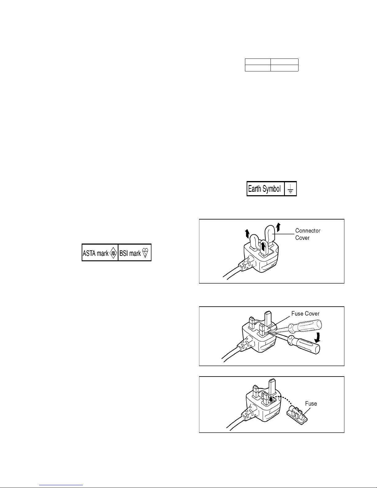
2.3.2. Caution for AC Mains Lead
For your safety, please read the following text carefully.
This appliance is supplied with a moulded three-pin mains plug
for your safety and convenience.
A 5-ampere fuse is fitted in this plug.
Should the fuse need to be replaced please ensure that the
replacement fuse has a rating of 5 amperes and it is approved
by ASTA or BSI to BS1362
Check for the ASTA mark or the BSI mark on the body of the
fuse.
If the plug contains a removable fuse cover you must ensure
that it is refitted when the fuse is replaced.
If you lose the fuse cover, the plug must not be used until a
replacement cover is obtained.
A replacement fuse cover can be purchased from your local
Panasonic Dealer.
If the fitted moulded plug is unsuitable for the socket outlet in
your home then the fuse should be removed and the plug cut
off and disposed of safety.
There is a danger of severe electrical shock if the cut off plug is
inserted into any 13-ampere socket.
If a new plug is to be fitted please observe the wiring code as
shown below.
If in any doubt, please consult a qualified electrician.
2.3.2.1. Important
The wires in this mains lead are coloured in accordance with
the following code:
As the colours of the wires in the mains lead of this appliance
may not correspond with the coloured markings identifying the
terminals in your plug, proceed as follows:
The wire which is coloured BLUE must be connected to the terminal in the plug which is marked with the letter N or coloured
BLACK.
The wire which is coloured BROWN must be connected to the
terminal in the plug which is marked with the letter L or coloured
RED.
Under no circumstances should either of these wires be connected to the earth terminal of the three pin plug, marked with
the letter E or the Earth Symbol.
2.3.2.2. Before Use
Remove the Connector Cover as follows.
2.3.2.3. How to Replace the Fuse
1. Remove the Fuse Cover with a screwdriver.
2. Replace the fuse and attach the Fuse cover.
Blue Neutral
Brown Live
6
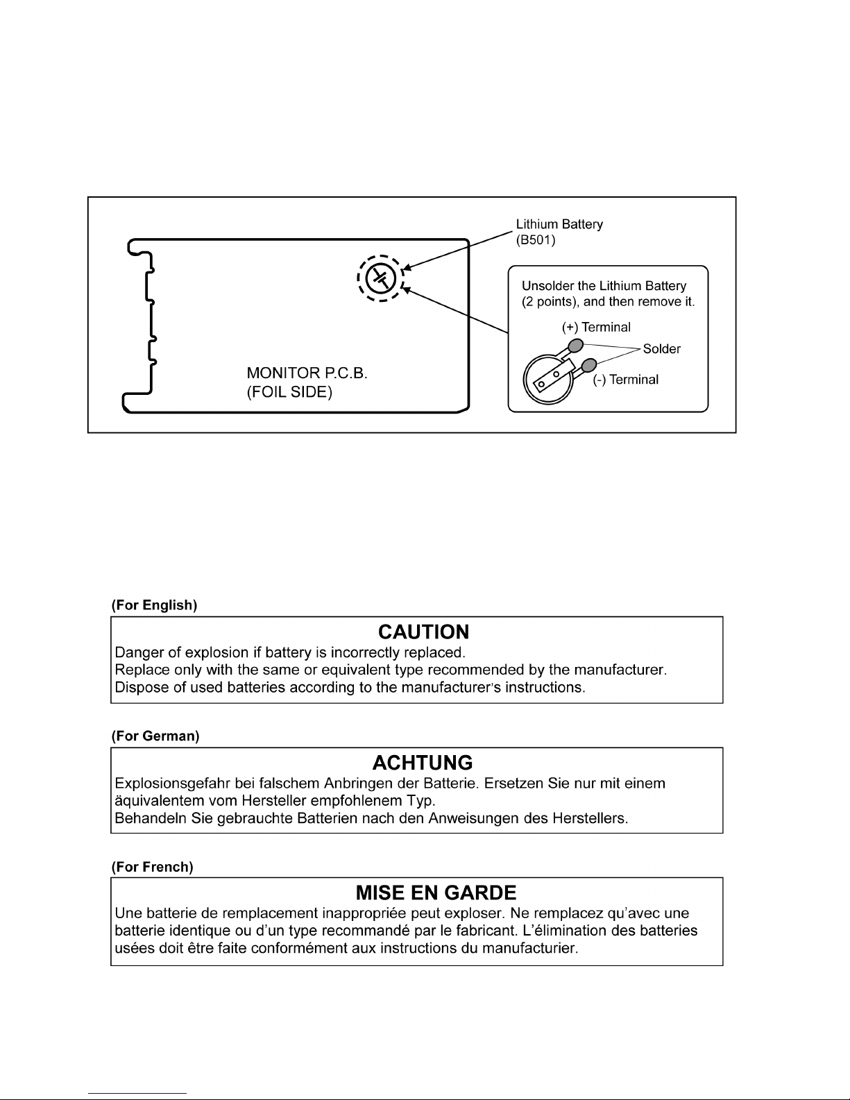
2.4. How to Replace the Lithium Battery
2.4.1. Replacement Procedure
1. Remove the MONITOR P.C.B.. (Refer to Disassembly Procedures.)
2. Unsolder the each soldering point of electric lead terminal for Lithium battery (Ref. No. “B501” at foil side of MONITOR
P.C.B.) and remove the Lithium battery together with electric lead terminal. Then replace it into new one.
NOTE:
The Type No. ML-614S/DN includes electric lead terminals.
NOTE:
This Lithium battery is a critical component.
(Type No.: ML-614S/DN Manufactured by Energy Company, Panasonic Corporation)
It must never be subjected to excessive heat or discharge.
It must therefore only be fitted in requirement designed specifically for its use.
Replacement batteries must be of same type and manufacture.
They must be fitted in the same manner and location as the original battery, with the correct polarity contacts observed.
Do not attempt to re-charge the old battery or re-use it for any other purpose.
It should be disposed of in waste products destined for burial rather than incineration.
NOTE:
Above caution is applicable for a battery pack which is for HC-W850/W858/W850M/V750/V757/V750M/V730 series, as well.
7
3 Service Navigation
3.1. Introduction
This service manual contains technical information, which allow service personnel’s to understand and service this model.
Please place orders using the parts list and not the drawing reference numbers.
If the circuit is changed or modified, the information will be followed by service manual to be controlled with original service manual.
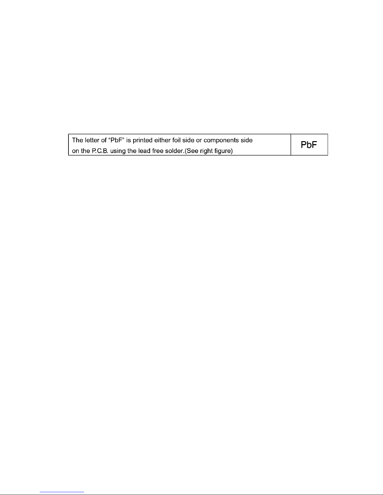
3.2. General Description About Lead Free Solder (PbF)
The lead free solder has been used in the mounting process of all electrical components on the printed circuit boards used for this
equipment in considering the globally environmental conservation.
The normal solder is the alloy of tin (Sn) and lead (Pb). On the other hand, the lead free solder is the alloy mainly consists of tin
(Sn), silver (Ag) and Copper (Cu), and the melting point of the lead free solder is higher approx.30°C (86°F) more than that of the
normal solder.
Distinction of P.C.B. Lead Free Solder being used
Service caution for repair work using Lead Free Solder (PbF)
• The lead free solder has to be used when repairing the equipment for which the lead free solder is used.
(Definition: The letter of “PbF” is printed on the P.C.B. using the lead free solder.)
• To put lead free solder, it should be well molten and mixed with the original lead free solder.
• Remove the remaining lead free solder on the P.C.B. cleanly for soldering of the new IC.
• Since the melting point of the lead free solder is higher than that of the normal lead solder, it takes the longer time to melt the
lead free solder.
• Use the soldering iron (more than 70W) equipped with the temperature control after setting the temperature at 350±30°C
(662±86°F).
Recommended Lead Free Solder (Service Parts Route.)
• The following 3 types of lead free solder are available through the service parts route.
RFKZ03D01KS-----------(0.3mm 100g Reel)
RFKZ06D01KS-----------(0.6mm 100g Reel)
RFKZ10D01KS-----------(1.0mm 100g Reel)
Note
* Ingredient: tin (Sn) 96.5%, silver (Ag) 3.0%, Copper (Cu) 0.5%, Cobalt (Co) / Germanium (Ge) 0.1 to 0.3%
8
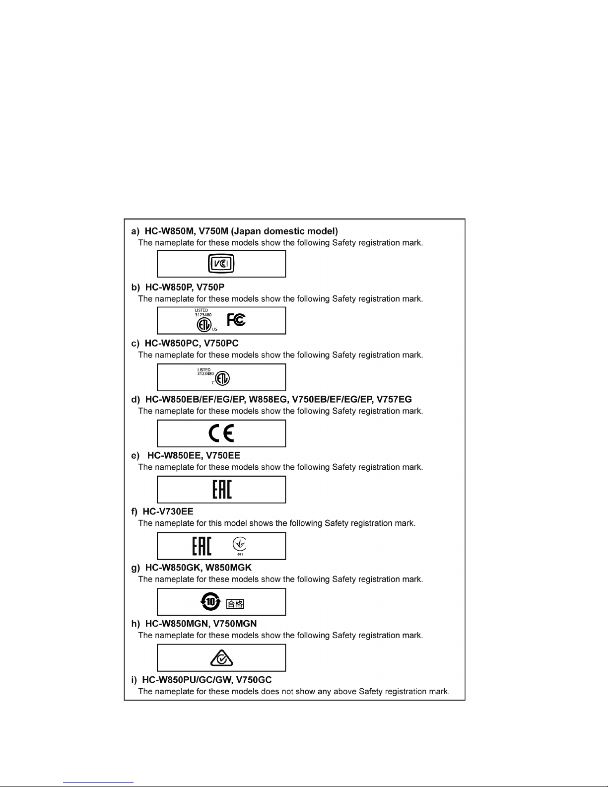
3.3. How to Define the Model Suffix (NTSC or PAL model)
There are nine kinds of HC-W850/W858/W850M/V750/V757/V750M/V730.
• a) HC-W850M, V750M (Japan domestic model)
• b) HC-W850P, V750P
• c) HC-W850PC, V750PC
• d) HC-W850EB/EF/EG/EP, W858EG, V750EB/EF/EG/EP, V757EG
• e) HC-W850EE, V750EE
• f) HC-V730EE
• g) HC-W850GK, W850MGK
• h) HC-W850MGN, V750MGN
• i) HC-W850PU/GC/GW, V750GC
What is the difference is that the “INITIAL SETTING” data which is stored in Flash ROM mounted on Main P.C.B..
3.3.1. Defining methods:
To define the model suffix to be serviced, refer to the rating label and caution label which are putted on the Unit.
NOTE:
After replacing the MAIN P.C.B., be sure to achieve adjustment.
9
3.4. Formatting
The following formatting is for HC-W850EB/EP, HC-V750EB/EP.
The page number in this page does not show the page number of this service manual.

10
3.5. Baking of replacement IC and defective P.C.B.
When replacing the CSP/BGA/QFN type IC mounted on the P.C.B., the problem of IC crack or foil pattern breaking in the P.C.B.
might sometimes occur by rapid heating.
In order to improve the success rate of IC replacement for repair, it would be required to work out baking of replacement
IC and defective P.C.B. before replacing IC.
Please refer the way of baking as follows.
Replacement IC and defective P.C.B. must be put in the heater together.
• Baking temperature and time (Hour)
80°C / 24 hour
11
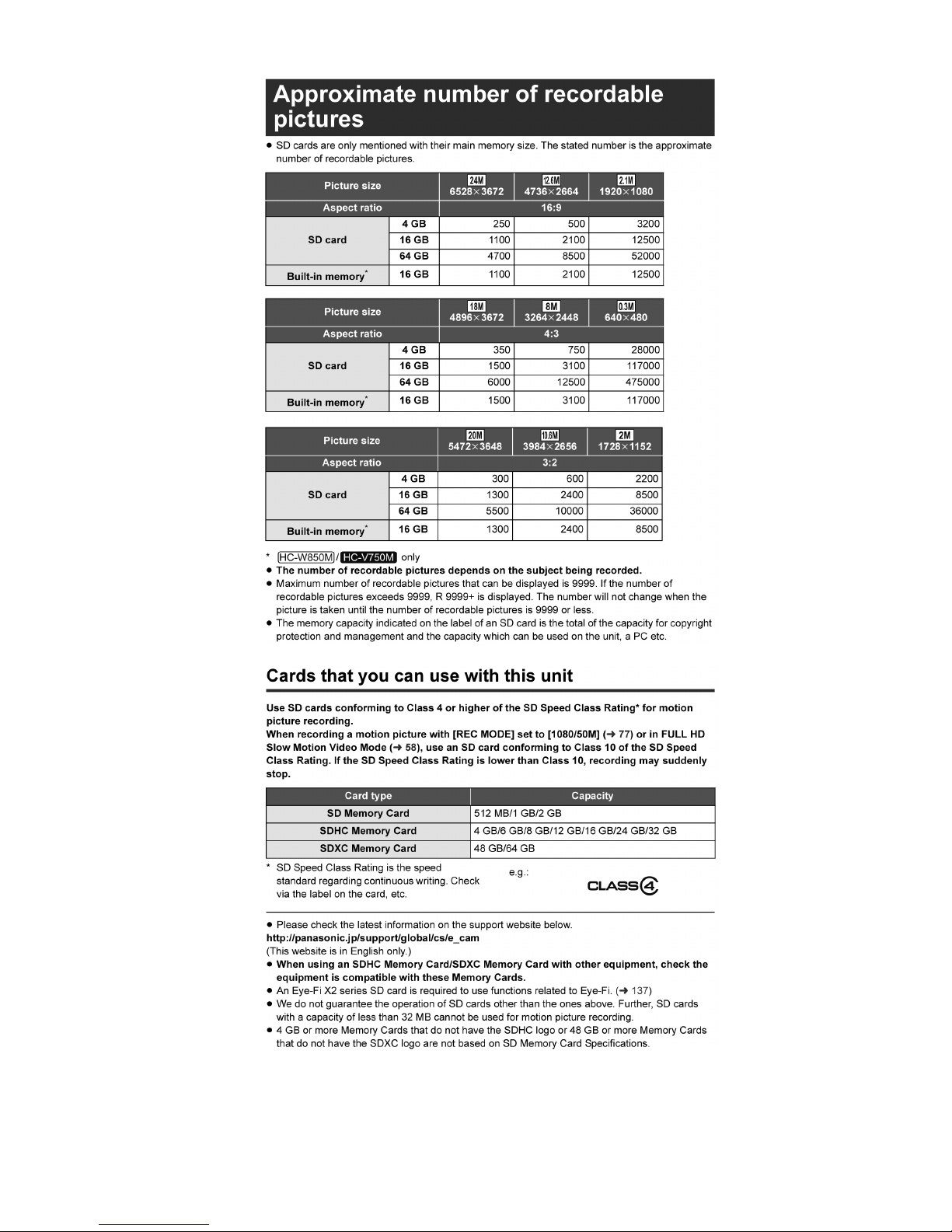
4 Specifications
The following specification is for HC-W850EB/EP, HC-V750EB/EP.
Some specifications may differ depending on model suffix.
The page number in this chapter does not show the page number of this service manual.

12
13

14
15

16
17
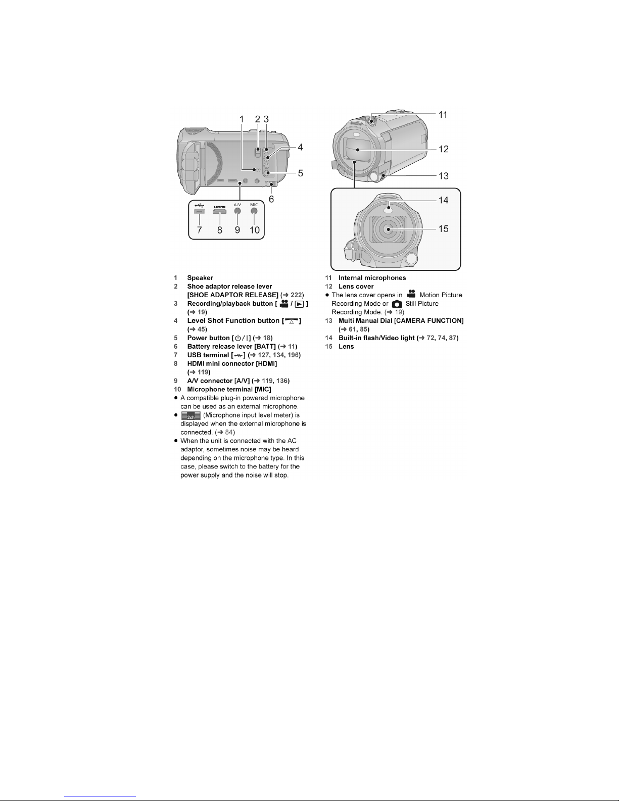
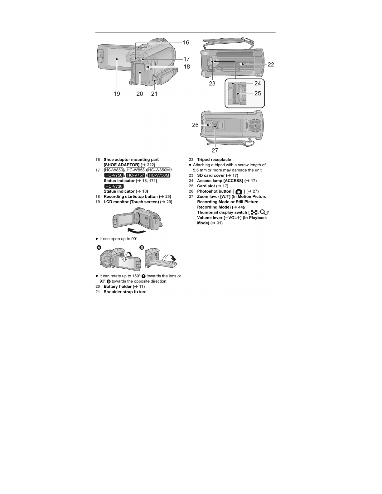
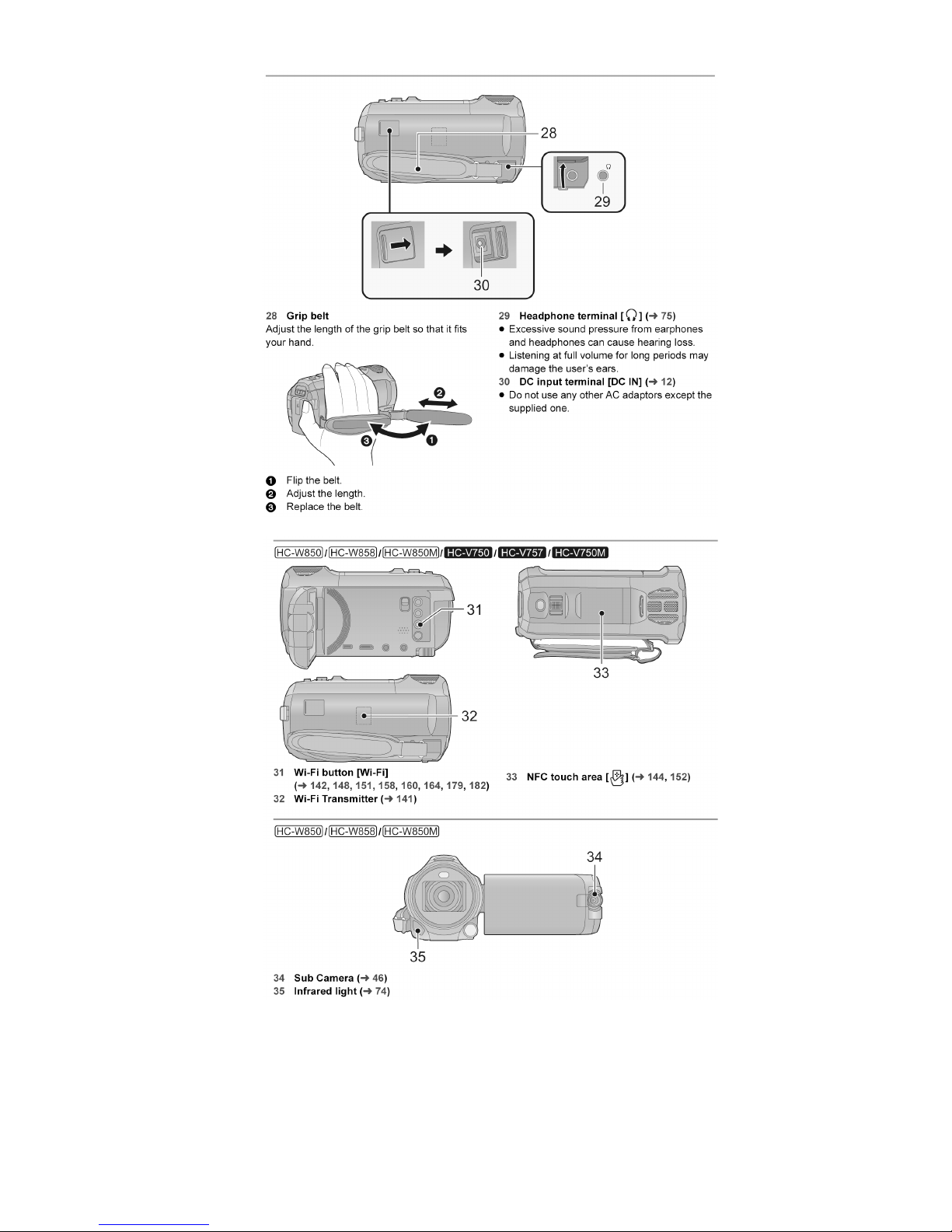
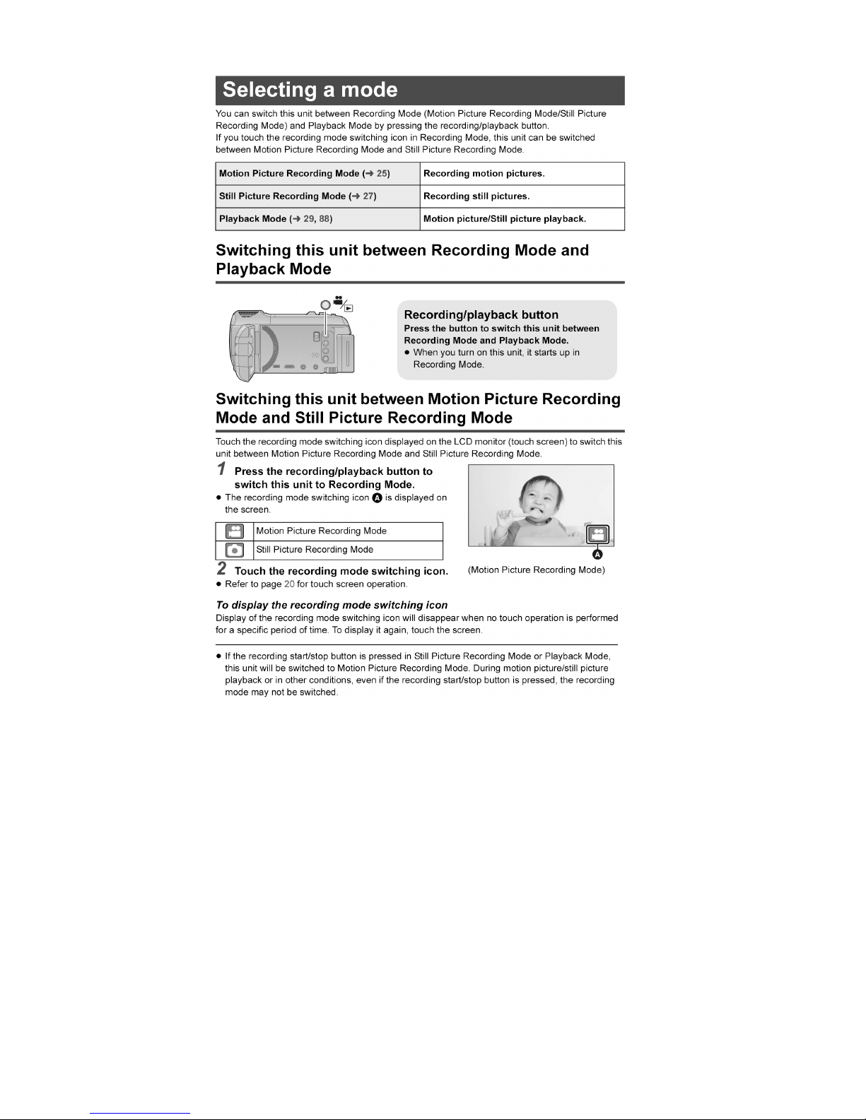
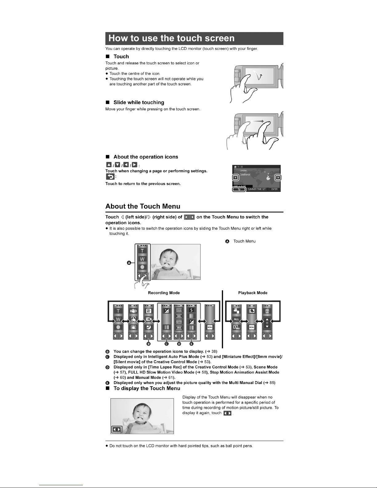
5 Location of Controls and Components
The following description is for HC-W850EB/EP, HC-V750EB/EP.
Some descriptions may differ depending on model suffix.
The page number in this chapter does not show the page number of this service manual.
18
19
20
21
22
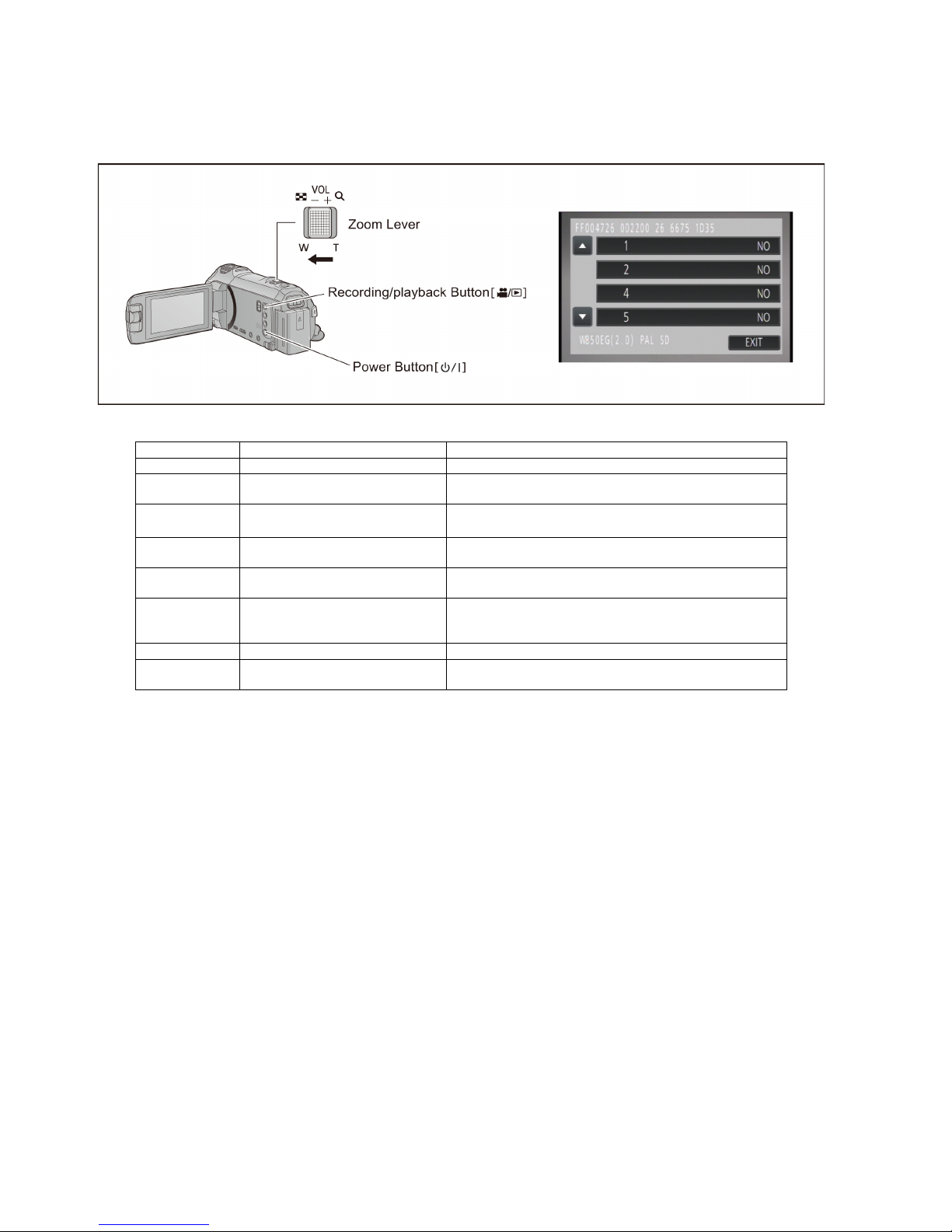
6 Service Mode
Indication method of the service menu
1. Keep pressing the “Power” button, “Zoom lever” to W side and “Recording/Playback” button for more than 3 seconds until the
top screen of the Service Mode Menu being displayed.
Service mode menu
(*)
HC-W850/W858/W850M only
NOTE:
Do not using service mode except above table of Service mode menu.
2. End method of the top screen of the service mode menu
Touch the [ EXIT ] of LCD to end the service mode, and then POWER OFF.
Screen display Contents Function
1 Factory settings Function to throw a product up in a factory shipment state.
2 Model/Destination settings Change the Model/Destination.
(Selectable models and destinations are displayed.)
4 Lock search history indication
Display the main and sub
(*)
camera system error cord for each
three histories saved in EEPROM.
5 Power ON self check result display Power ON self check (function to diagnose correct function of the
device and interface between devices) result display.
14 Adjutment function for the service The service adjustment do setup and adjustment of the following
items required in the field service.
15 Restore the backed up adjustment data Restore the adjustment data to new or repaired Main P.C.B. from
SD card that the data backed up from original Main P.C.B. before
repairs or replacement.
16 Touch panel calibration Calibrate the touch positions of the touch panel.
17 NFC initialization
(except HC-V730)
Performs the Initialization of the NFC chip and erase the settings
like as Wi-Fi connection etc..
23
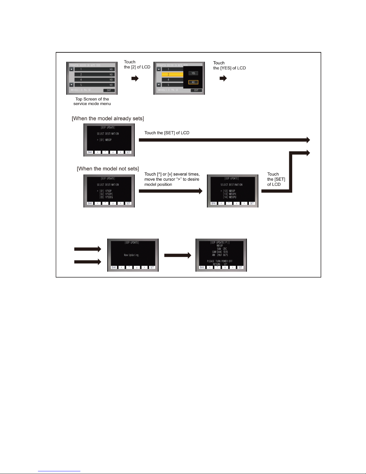
6.1. Model/Destination Settings
Touch the [ 2 ] of LCD, select model/destination settings.
Operation specifications
Function description
• Change the Model/Destination
Display the lists of model/distination which the unit can be changed, if a shipment setup is finished.
Therefore in some cases, the model/destination that is currently set is only displayed.
End method of operation
• Touch the [ SET ] of LCD to exit the mode/destination settings, and then POWER OFF.

24
6.2. Lock Search and Error History Indication
Touch the [ 4 ] of LCD, select Lock search and error history indication.
Operation specifications
Indication contents
1. Main Camera
• Lock search history indication of main camera
Display the main camera system error cord for three histories saved in EEPROM.
• The error cord contents which are displayed
2. Sub Camera (HC-W850/W858/W850M only)
• Lock search history indication of sub camera
Display the sub camera system error cord for three histories saved in EEPROM.
(Display always “--” for no sub camera models.)
• The error cord contents which are displayed
End method of operation
• Touch the [ BAK ] of LCD to exit the lock search and error history indication, and then POWER OFF.
Error code Description
51 Focus control is abnormal
52 Zoom control is abnormal
53 OIS lens control is abnormal
54 Zoom control is abnormal (2)
71 Lens barrier open/close is abnormal
Error code Description
91 Sub camera error

25
6.3. Power ON Self Check Result Display
Touch the [ 5 ] of LCD, select Power ON self check result display.
Operation specifications
Indication contents
• Power ON self check result display
Function to diagnose correct function of the device and interface between devices result display.
Display the following communication test result.
- Power IC : Communication test between IC3401 and IC1503
- Main IC : DDR. Communication test between IC3401 and IC3402/IC3403
- WiFi IC : Communication test between IC3401 and Wi-Fi P.C.B.. (except HC-V730)
- NFC IC : Communication test between IC3401 and NFC P.C.B. unit. (except HC-V730)
Display other than “OK” are abnomalities of each lines.
- PanTilter : Error display of the Remote Pan Tilt Cradle (VW-CTR1)
(When not connected the remote pan tilt cradle, display “--”.)
When error is occurred, display “NG” with the error code.
End method of operation
• Touch the [ BAK ] of LCD to exit the power on self check result display, and the POWER OFF.
Error Code Description
NG 01 Battery undercut
NG 04 The start-up state of the update error factor
NG 10 The failure of Tilt motor
NG 80 USB Communication Error

26
6.4. Adjustment function for the Service
Touch the [14] of LCD, select the adjustment function for the service.
Operation Specifications (until before the start of the adjustment)
Function description
The service adjustment do setup and adjustment of the following items required in the field service.
For a detailed content, such as the adjustment procedure, refer to “9 Measurements and Adjustments”.
• Model setting
• Setting of the file name for adjustment data backup to SD card.
• Execution of adjustment data backup to SD card
• Checking of Switches
• Camera adjustment (Iris, Gyro, OIS and Missing pixels)
• Zoom Tracking adjustments (with Zoom hysteresis adjustment)
• Indoor White Balance Adjustment (CH-GAIN, PWM, WB)
• Outdoor White Balance Adjustment (PWM, WB)
• Level shot adjustment
End method of operation
• Press the power button to turn the unit off.

27
6.5. Restore the backed up adjustment data
Touch the [15] of LCD, select restoring the backed up adjustment data from SD card to the unit.
Operation Specifications
Function description
Restore the adjustment data to new or repaired Main P.C.B. from SD card that the data backed up from original Main P.C.B.
before repairs or replacement.
To backup the adjustment data, use “6.4. Adjustment function for the Service”.
Restoring procedure
End method of operation
• Press the power button to turn the unit off.

28
6.6. Touch Panel Calibration
Touch the [16] of LCD, select the calibration of touch panel.
Operation Specifications
Function description
Calibrate the touch positions of the touch panel.
End method of operation
• Press the power button to turn the unit off.
6.7. NFC Initialization (except HC-V730)
Touch the [17] of LCD, select initialization of NFC (Near Field Communication) function.
Operation Specifications
Function description
This function performs the Initialization of the NFC chip and erase the settings like as Wi-Fi connection etc..
End method of operation
• Press the power button to turn the unit off.

29
7 Service Fixture & Tools
7.1. When Replacing the Main P.C.B.
After replacing the MAIN P.C.B., be sure to achieve adjustment.
7.2. Service Position
This Service Position is used for checking and replacing parts. Use the following Extension cables for servicing.
7.2.1. Extention Cable Connection
No. Parts No. Connection Form
1 RFKZ0354 FP6001(MAIN) - MONITOR FPC 37PIN 0.3 FFC
1 RFKZ0354 FP201(MAIN) - MONITOR FPC (HC-W850/W858/W850M only) 37PIN 0.3 FFC
2 VFK1581 PP6001(MAIN) - PS6401(SD HOLDER) 60PIN 0.5 B to B
3 VFK1388 FP6012(MAIN) - FRONT FFC 12PIN 0.5 FFC
4 VFK1440 FP4803(SD HOLDER) - TOP CASE UNIT 10PIN 0.5 FFC

30
8 Disassembly and Assembly Instructions
8.1. Disassembly Flow Chart for the Unit
This is a disassembling chart.
When assembling, perform this chart conversely.

31
8.2. PCB Location

32
8.3. Disassembly Procedure for the
Unit
No. Item Fig. Removal
1 Side Case-L Unit (Fig. D1) Screw (A) x 3
Screw (B) x 2
(Fig. D2) Screw (C) x 3
Locking tab x 3
Side Case-L Unit
(Fig. D3) Screw (D) x 1
Jack Cover Piece
Locking tab x 1
SS Lever
SS Button
Jack Door Spring
DC Jack Cover Unit
Screw (E) x 2
HP Jack Cover Piece
HP Jack Cover
Locking tab x 2
(HC-W850/W858/W850M
only)
IR Piece
(HC-W850/W858/W850M
only)
2 Top Case,
Top Operation
(Fig. D4) Screw (F) x 1
Screw (G) x 1
Screw (H) x 1
Locking tab x 1
(Fig. D5) Projection part x 2
FP4803 (Flex)
(Fig. D6) Screw (I) x 4
Convex x 2
Top Shoe Angle
Screw (J) x 3
Top Operation
Power Panel Light
Shoe Cover
Cover Open Spring
Locking tab x 1
Top Ornament
Top Case
3 Front Case Unit (Fig. D7) Screw (K) x 1
Screw (L) x 2
(Fig. D8) Flex A
Lead wire A
Screw (M) x 1
Locking tab x 1
Convex x 1
FP6012 (Flex)
Front Case Unit
4 (except HC-V730)
NFC P.C.B. Unit,
Wi-Fi P.C.B.
(Fig. D9) Screw (N) x 1
FP6007 (Flex)
Hooking part x 1
NFC P.C.B. Unit
Screw (O) x 1
Flex B
Hooking part x 1
Wi-Fi P.C.B.
5 Photo Light DRV. P.C.B.
Unit
(Fig. D10) Screw (P) x 2
Flex C
Photo Light DRV. P.C.B.
Unit
6 Wi-Fi Frame Unit
Lens Frame Unit,
Barrier Motor Unit
(Fig. D11) Screw (Q) x 2
Convex x 3
Hooking part x 2
(Fig. D12) Wi-Fi Frame Unit
Screw (R) x 1
Hooking part x 3
FP6005 (Flex)
(Fig. D13) Screw (S) x 2
Lens Frame Unit
Barrier Motor Unit
7 Camera Lens Unit (Fig. D14) FP6001 (Flex)
FP301 (Flex)
Convex x 2
Camera Lens Unit
8Main P.C.B.,
SD Holder P.C.B.
(Fig. D15) Screw (T) x 5
Hooking part x 3
Heat Radiation Plate Unit
(Fig. D16) P6003 (Connector)
P6401 (Connector)
FP201 (Flex)
(HC-W850/W858/W850M
only)
FP6001 (Flex)
Hooking part x 1
FP611 (Flex)
(HC-W850M/V750M
only)
(Fig. D17) Main P.C.B.
SD Holder P.C.B.
9 (HC-W850M/V750M only)
ESD P.C.B. Unit
(Fig. D18) Screw (U) x 1
ESD P.C.B. Unit
10 BR Frame Unit,
Speaker,
LCD Unit
(Fig. D19) Screw (V) x 2
Screw (W) x 2
Screw (X) x 2
Locking tab x 2
Convex x 4
(Fig. D20) BR Frame Unit
Shoe Lock Knob
Shoe Lock Spring
Speaker
LCD Lever
Convex x 3
(Fig. D21) Convex x 2
LCD Unit
11 BATT. Catcher P.C.B. (Fig. D22) Hooking part x 2
BATT. Frame
BATT. Catcher P.C.B.
12 (HC-W850/W858/W850M)
LCD Hinge Unit,
Sub Camera Unit
(Fig. D23) Screw (Y) x 2
Screw (Z) x 2
Locking tab x 9
LCD Case (T) Unit
FP251 (Flex)
FP901 (Flex)
(Fig. D24) LCD Hinge Unit
Screw (a) x 1
Convex x 3
LCD Frame A
FP252 (Flex)
Convex x 1
Sub Camera Unit
No. Item Fig. Removal

33
13 (HC-V750/V757/V750M/
V730)
LCD Hinge Unit
(Fig. D25) Screw (Y) x 2
Screw (Z) x 2
Locking tab x 9
LCD Case (T) Unit
FP901 (Flex)
(Fig. D26) LCD Hinge Unit
Screw (a) x 1
Convex x 3
LCD Frame A
14 Monitor P.C.B.,
LGP Unit,
LCD
(Fig. D27) FP904 (Flex)
FP905 (Flex)
Locking tab x 1
Hooking part x 1
Monitor P.C.B.
Locking tab x 4
LGP Unit
LCD
Convex x 1
SC Rotate Earth Plate
(HC-W850/W858/W850M
only)
(Fig. D28) Reflection Sheet
Light Guide Plate
Diffusion Sheet
Prism Sheet (B)
Prism Sheet (A)
LGP Holder
15 Mic P.C.B. (Fig. D29) Screw (b) x 1
FP4802 (Flex)
Mic P.C.B.
16 Front Base,
Barrier R,
Barrier F,
Photo Light P.C.B.
(Fig. D30) Projection part x 3
Lens Damper Rubber
Screw (c) x 5
(Fig. D31) Front Base
Barrier R
Barrier F
Hooking part x 1
Convex x 2
Photo Light P.C.B.
17 Front Ring,
Hood Piece
(Fig. D32) Screw (d) x 2
Front Ring
LED Light Lens
Convex x 2
Locking tab x 6
LED Light Cover
Hood Piece
Hood Mask
18 Front Case,
Front Ornament Unit
Mic Case Unit
(Fig. D33) Screw (e) x 1
Screw (f) x 1
Convex x 1
Locking tab x 1
Convex x 2
Locking tab x 1
Front Case
Locking tab x 2
MF Ornament
Front Ornament Unit
(Fig. D34) Screw (g) x 2
Mic Earth Plate
Mic Case Unit
Mic Net Cover
No. Item Fig. Removal
19 Kurupon Unit,
Front P.C.B.
(Fig. D35) Screw (h) x 2
Locking tab x 2
Convex x 2
FR Earth Angle
Kurupon Unit
Locking tab x 1
Convex x 2
Front P.C.B.
20 MOS Unit (Fig. D36) Screw (i) x 3
Convex x 2
MOS Unit
21 (HC-W850/W858/W850M )
IR Kudou Unit
(Fig. D37) Solder x 2 points
Screw (j) x 1
Convex x 2
IR Kudou Unit
22 2nd Stepping Motor (Fig. D38) Solder x 4 points
Screw (k) x 3
2nd Stepping Motor
23 3rd Stepping Motor (Fig. D39) Solder x 4 points
Screw (m) x 3
Convex x 1
3rd Stepping Motor
24 4th Stepping Motor (Fig. D40) Solder x 4 points
Screw (n) x 2
Convex x 2
4th Stepping Motor
No. Item Fig. Removal

34
8.3.1. Removal of the Side Case-L Unit
(Fig. D1)
(Fig. D2)

35
(Fig. D3)
8.3.2. Removal of the Top Case, Top
Operation
(Fig. D4)

36
(Fig. D5)
(Fig. D6)

37
8.3.3. Removal of the Front Case Unit
(Fig. D7)
(Fig. D8)

38
8.3.4. (except HC-V730) Removal of the
NFC P.C.B. Unit, Wi-Fi P.C.B.
(Fig. D9)
8.3.5. Removal of the Photo Light DRV.
P.C.B. Unit
(Fig. D10)
8.3.6. Removal of the Wi-Fi Frame Unit,
Lens Frame Unit, Barrier Motor Unit
(Fig. D11)

39
(Fig. D12)
(Fig. D13)

40
8.3.7. Removal of the Camera Lens Unit
(Fig. D14)
8.3.8. Removal of the Main P.C.B., SD
Holder P.C.B.
(Fig. D15)

41
(Fig. D16)
(Fig. D17)
8.3.9. (HC-W850M/V750M only) Removal
of the ESD P.C.B. Unit
(Fig. D18)

42
8.3.10. Removal of the BR Frame Unit,
Speaker, LCD Unit
(Fig. D19)
(Fig. D20)

43
(Fig. D21)
8.3.11. Removal of the BATT. Catcher
P. C .B.
(Fig. D22)
8.3.12. (HC-W850/W858/W850M) Removal
of the LCD Hinge Unit, Sub Camera
Unit
(Fig. D23)

44
(Fig. D24)
8.3.13. (HC-V750/V757/V750M/V730)
Removal of the LCD Hinge Unit
(Fig. D25)

45
(Fig. D26)
8.3.14. Removal of the Monitor P.C.B., LGP
Unit, LCD
(Fig. D27)

46
(Fig. D28)
8.3.15. Removal of the Mic P.C.B.
(Fig. D29)

47
8.3.16. Removal of the Front Base, Barrier
R, Barrier F, Photo Light P.C.B.
(Fig. D30)
(Fig. D31)

48
8.3.17. Removal of the Front Ring, Hood
Piece
(Fig. D32)
8.3.18. Removal of the Front Case, Front
Ornament Unit, Mic Case Unit
(Fig. D33)

49
(Fig. D34)
8.3.19. Removal of the Kurupon Unit, Front
P.C.B.
(Fig. D35)

50
8.3.20. Removal of the MOS Unit
(Fig. D36)
8.3.21. (HC-W850/W858/W850M) Removal
of the IR Kudou Unit
(Fig. D37)
8.3.22. Removal of the 2nd Stepping Motor
(Fig. D38)

51
8.3.23. Removal of the 3rd Stepping Motor
(Fig. D39)
8.3.24. Removal of the 4th Stepping Motor
(Fig. D40)

52
9 Measurements and Adjustments
9.1. Electric Adjustment
• Adjustment method is different from a conventional High definition video camera.
• An exclusive jig are necessary for electric adjustment.
• Connection method of the main unit and an exclusive adjustment jig as follows.
Figure of connection
Figure of image when adjustment

53
Part Number of jig
1. Basic Jig
2. Optical Jig for Camera Adjustment
* RFKZ0523 (same as DSC) is recommended.
Item Contents
AC adaptor Bandled with camcorder
AC Cable Bandled with camcorder
Item Part number Remarks
Light box VFK1164TDVLB/RFKZ0523* Need external power supply: 12V ± 0.1V /1.8A or over
Collimator with focus chart VFK1164TCM02/VFK1164TCM03 Same as DSC
CC filter 3100K/5100K VFK1164CC10G Need 2 set. For indoor/outdoor white balance adjutment
C2 Filter 5100K VFK1164LBB2 For outdoor white balance adjustment
C8 Filter 5100K VFK1164LBB8 For outdoor white balance adjustment
ND Filter 0.1 3100K VFK1164ND01 For indoor white balance adjustment
ND Filter 0.6 3100K VFK1164ND06 For indoor white balance adjustment
Adjustment chart for Level Shot Bandled with this Manual For Level shot adjustment

54
[Level Shot Adjutment Chart]

55
9.1.1. About Light Box
When using VFK1164TDVLB Light Box
If using VFK1164TDVLB Light Box, remove the lens connection ring by loosing thumbscrew and three hexagon screws.
* RFKZ0523 Light Box has no lens connection ring.
How to remove the Front Hood
In order to utilize maximum of the diffusing surface of light box, some adjustment items need the distance between diffusing
surface of light box and camera body becomes several cent-meters.
Before the adjustments, remove the front hood of light box following steps below.
[ For VFK1164TDVLB Light Box ]
[ For RFKZ0523 Light Box ]

56
9.1.2. Adjustment Items
Adjustment item as follows.

57
9.1.3. Adjustment Procedure
All adjustments except “Touch Panel Calibration”, “Factory Setting” and “NFC Initialization” performs using “14 Adjustment function
for the service” in service mode menu.
“Touch Panel Calibration” is performed using 16 of service mode menu and “Factory Setting” is performed using 1, “NFC Initialization” is performed using 17 of service mode menu. Refer to “6 Service mode” and “10 Factory Setting”.
[Execute adjustment function for service]
1. While the power is turned OFF, keep pressing the “Power” button, “Zoom lever” to W side and “Recording/Playback” button
for more than 3 seconds until the top screen of the Service Mode Menu being displayed.
2. Touch the twice then touch the [14] of LCD.
3. Touch the [YES] of LCD.

58
[Adjustment Procedure]
Adjustments and settings are performed following order:
1. Model setting
2. Filename setting for backup to SD card
3. Backing up adjustment data to SD card
4. Checking switches
5. Camera adjustment (Iris, Gyro, OIS, Missing pixels)
6. Zoom/tracking adjustment (with Zoom hysteresis adjustment)
7. Indoor white balance adjustment (CH GAIN, PWM, WB)
8. Outdoor white balance adjustment (PWM, WB)
9. Level shot adjustment

59

60

61

62

63

64

65

66
10 Factory Setting
10.1. How To Turn On The Factory Settings?
1. While the power is turned OFF, keep pressing the “Power” button, “Zoom lever” to W side and “Recording/Playback” button for
more than 3 seconds until the top screen of the Service Mode Menu being displayed.
2. Touch the [ 1 ] of LCD.
3. Touch the [ YES ] of LCD.
4. After few seconds “END” is displayed or “ESD NODATA” as “NG” is displayed on LCD monitor. Cutting of battery connection
or AC power supply connection as a completion of the “FACTORY SETTINGS”.
(After recording at least once, even if the physical format of the build-in memory will be performed, “ESD NODATA” as “NG” is
indicated, but “FACTORY SETTINGS” is completed.)

67
10.2. What Is The Factory Settings?
The factory settings clean up and/or refresh the following settings.
1. Setting Values of menu.
2. Clear the time and date setting.
3. Close the lens cover
4. Initialize the Wi-Fi data settings (except HC-V730)
5. Initialize the NFC data settings (except HC-V730)
6. Confirm that the data area of built-in memory is cleared. (HC-W850M/V750M only)
7. Confirm that the built-in memory cappacity is correct. (HC-W850M/V750M only)
(Checking of the built-in memory mounting error.)
(HC-W850M/V750M only)
If the “Factory Settings” is completed, physical format of the build-in memory is not performed, execute physical format according to
the following procedure.

68
11 Block Diagram
11.1. Overall Block Diagram
HC-W850/W858/W850M/V750/V757/V750M/V730 OVERALL BLOCK DIAGRAM
NOTE
: VIDEO SIGNAL
: AUDIO SIGNAL
: CLK or CONTROL LINE
IRIS
LENS(F1.8-3.6 20x)
IC701,706,763
LENS/OIS/MOTOR DRIVE
LED FLASH
DRIVER
SD
CARD
SPEAKER
ECM
OPERATION
TOUCH PANEL
DC IN
BATTERY
FLASH
MOS IMAGE
SENSOR
A/V
TERMINAL
ZOOM/
FOCUS
MOTOR/
OIS
Analog
Analog
Analog
Analog
IC6401
GYRO
SENSOR
(PIT/YAW)
IC751
GYRO
SENSOR
(ROLL)
IC1551
BATTERY
MONITOR
LED LIGHT
X3402
OSC
(72MHz)
IC302
GATE IC
IC205,252
GATE IC
SUB CAMERA
IC3413
GATE IC
IC6411
DIGITAL
ACCELEROMETER
IC901
LCD COLOR
DRIVER
COLOR LCD
PANEL
IC3701
AVIO
X2303
(32.768kHz)
IC1503
RTC/CHARAGE/
POWER CONTROL
IC4802,4803
MIC AMP
EXT.
MIC
Q4901-4904,
4907,4908
MIC AMP
Analog Analog
IC2301
RESET
IC1501
REGULATOR
IC761
ROLL GYRO AMP
BARRIER
IC705
LENS BARRIER
DRIVE
USB TERMINAL
HDMI mini
CONNECTOR
IC1001
POWER
IC301,703,704,1003,1221,1241,1261,1262,1291,1341,1392,3412
POWER CONT. LOGIC SW/REGULATOR/
SYNCHRONOUS STEP DOWN CONVERTER
IC1002,1381
SWITCHING REGULATOR/REGULATOR
IC1471
POWER-DISTRIBUTION
SWITCHES
IC3401
VENUS ENGINE
(POP: DDR2 SDRAM 4Gbit)
Wi-Fi ANT.
NFC
NFC ANT.
NFC P.C.B. UNIT
Wi-Fi
MODULE
Wi-Fi P.C.B.
IC3404
NAND FLASH ROM/
1Gbit
MOS IMAGE
SENSOR
IC203
CAMERA
BRIDGE IC
IC762
MOTOR DRIVE
IR FILTER
HC-W850/W858/W850M only
Q6501,6502
QR6501,6502
IR LIGHT DRIVE
IR LIGHT
HC-W850/W858/W850M only
IC1222,3406
RESET
IC201,202,206,207,208
REGULATOR
HC-W850/W858/W850M only
IC3702
CLOCK GENERATOR
IC3703
VIDEO AMP
HC-W850/W858/W850M only
PHOTO LIGHT DRV. P.C.B. UNIT
except HC-V730
except HC-V730
INTERNAL MEMORY
/16GB
ESD P.C.B. UNIT
HC-W850M/V750M only
except HC-V730

69
11.2. Camera Circuit Block Diagram
HC-W850/W858/W850M/V750/V757/V750M/V730 CAMERA CIRCUIT BLOCK DIAGRAM
IC3401
(VENUS ENGINE)
G27
LVDS RXCAP
LVDS RXCAM
LVDS RX0P
LVDS RX0M
LVDS RX9M
LVDS RX9P
LVDS RX8P
LVDS RX8M
LVDS RX7M
LVDS RX7P
G26
E27
X3402
(72MHz)
E26
J26
J27
K24
K25
J25
J24
RL3401 RL3402RL3403 RL3404 RL3407 RL3408
IS HD
A23
SENS LVDSCAP
SENS LVDSCAM
SENS LVDS0P
SENS LVDS0M
SENS LVDS2P
SENS LVDS2M
SENS LVDS3P
SENS LVDS3M
SENS LVDS1P
SENS LVDS1M
H26
LVDS RX5M
LVDS RX5P
LVDS RX6M
LVDS RX6P
LVDS RX1M
LVDS RX1P
LVDS RX2M
LVDS RX2P
LVDS RX4P
LCDS RX4M
H27
H24
H25
G25
G24
E24
E25
F26
F27
RL3406 RL3405
SENS LVDS4P
SENS LVDS4M
SENS LVDS5P
SENS LVDS5M
SENS LVDS7P
SENS LVDS7M
SENS LVDS8P
SENS LVDS8M
XHD CAM
IS VD
B23
XVD CAM
DO SENS
C22
S SENS SDO
CLK SENS
A22
S SENS SCK
CS SENS
B22
S SENS CS
MOS RST
C23
E MOS RST
SENS LVDS6P
SENS LVDS6M
LVDS RX3M
LVDS RX3P
F24
F25
SENS LVDS9P
SENS LVDS9M
XHS
XVS
SDI
SCK
XCE
XCLR
INCK (72MHz)
IC203
(CAMERA BRIDGE IC)
AE14
Y0
Y1
Y2
Y3
Y6
Y7
C0
C1
Y4
Y5
AD14
AG13
51
50
49
PD 0
PD 1
PD 2
AF13
AE13
AD13
54
53
52
PD 3
PD 4
PD 5
AG12
55
PD 6
MIPI D0P
BUS648 D0P
AF12
AE12
AD12
58
57
56
PD7
PD 8
48
PD 9
BUS20 WCAMY0
WCAM PONH18
WCAM PONH18
BUS20 WCAMY1
BUS20 WCAMY2
BUS20 WCAMY3
BUS20 WCAMY6
BUS20 WCAMY7
BUS20 WCAMC0
BUS20 WCAMC1
BUS20 WCAMY4
BUS20 WCAMY5
AG11
C2
C3
C4
C5
HD
VD
CLK27 WCAM
RESX MIPY
C6
C7
AF11
AE11
61
60
59
PD 10
PD 11
PD 12
AD11
AF10
AE10
64
63
62
PD 13
PD 14
PD 15
AF14
38
HSYNC
AA9
AG14
AG5
34
35
37
VSYNC
PCLK
RESX
BUS20 WCAMC2
BUS20 WCAMC3
BUS20 WCAMC4
BUS20 WCAMC5
MIPI HD
MIPI VD
CLK40 MIPI
RESX MIPI
BUS20 WCAMC6
BUS20 WCAMC7
CLK40 MIPI
D22
36
REFCLK
CLK27 WCAMCLK27 WCAM1
5
143 2
IC302
(GATE IC)
PW MOS1.8V-1
PW CAM2.1V
PW MIPI1.8V
FCK
R27
CLK72 MOS
5
143 2
IC252
(GATE IC)
PW WCAM1.8V
5
143 2
IC205
(GATE IC)
PW MIPI1.8V
SUB CAM UNIT
MOS UNIT
CH204
CH251
CH215
CH213
CH252
CH216CH219
CH253
CH214CH254
CH206
CH208
CH212 CH211 CH210 CH217 CH218
S WCAM SDA
B11
32
I2C SDA
S WCAM SDA
S WCAM SCK
A11
WCAM PDZ
AE5
31
I2C SCL
SDA
TD1 P
TD1 M
TD2 P
TD2 M
TCK P
TCK M
SCL
PDZ
INT
WCAM FOCUS
WCAM ONL
S WCAM SCK
WCAM PDZ
WCAM RST
AF5
RSTX
EXCLK
WCAM FOCUS
WCAM RST
WCAM CLK27 ON
B13
WCAM CLK27 ON
WCAM INT
A13
WCAM INT
WCAM FOCUS
N2
WCAM ONL
G1
MIPI D0N
BUS648 D0N
47
MIPI D1P
BUS648 D1P
46
MIPI D1N
BUS648 D1N
45
MIPI CP
BUS648 CKP
40
MIPI CN
BUS648 CKN
39
5
1
4
3
2
IC202
(REGULATOR)
GND
VOUT
NC
VIN
CTL
AB11
WCAM PONH12
MOSSENS ON H
WCAM PONH12
PW REG1.8V
PW MIPI1.2V1
5
1
4
3
2
IC201
(REGULATOR)
GND
VOUT
NC
VIN
CTL
C13
WCAM PONH28
WCAM PONH28
PW 3.2V
PW WCAM2.8V
5
1
4
3
2
IC206
(REGULATOR)
GND
VOUT
NC
VIN
CTL
AB10
WCAM PONH30
WCAM PONH130
PW 3.2V
PW WCAM3.0V
5
1
4
3
2
IC207
(REGULATOR)
GND
VOUT
NC
VIN
CTL
AA10
WCAM PONH185
WCAM PONH185
PW CAM2.1V
PW WCAM1.85V
5
1
4
3
2
IC208
(REGULATOR)
GND
VOUT
NC
VIN
CTL
AA11
PW MOS2.8VA
5 4
1 32
IC301
(REGULATOR)
NC
IN
OUT
GNDCE
PW 3.2V
MOSSENS ON H
C12
LVDS CKP
LVDS CK M
LVDS A P
LVDS A M
LVDS B P
LVDS B M
LVDS C P
LVDS C M
LVDS D P
LVDS D M
LVDS E P
LVDS E M
LVDS F P
LVDS F M
LVDS G P
LVDS G M
LVDS H P
LVDS H M
LVDS I P
LVDS I M
LVDS J P
LVDS J M
CH3423 CH3422
SUB CAM ON
HC-W850/W858/W850M only

70
11.3. System Control Circuit Block Diagram
HC-W850/W858/W850M/V750/V757/V750M/V730 SYSTEM CONTROL CIRCUIT BLOCK DIAGRAM
X2303
(32.768kHz)
PW REG3V
S6001
LCD OPEN/CLOSE
CARD LED B
STANDBYLED B
KEYIN2
KEYIN4
POWER LED B
D6401
CARD
LED
D6501
IR
LED
PW REG3V
PW 3.2V
QR6402
FP4803
STANDBY LED
AVREF
AVREF
VTR KEY 4
ZOOMAD
1
2
4
5
FP905
X RIGHT
Y BOT
X LEFT
Y TOP
1
2
3
4
9
10
POWER LED
PW REG3V
PW REG1.8V
PW REG3V
P1
AE6
AF6
AG6
AD7
V6
V7
W7
W6
C21
F19
PW REG1.8V
QR6006
QR6403
R4
QR3413 QR3411
QR3412
QR3410
QR6008
D21
TOUCH PANEL
UNIT
QR6007
Wi-Fi
S6404
BALANCE SHOT
S6402
B19
IC1503
(RTC/CHARGE/POWER CONTROL)
S6401
POWER ON/OFF
D3
G5
G6
/SWIN1
E3
/SWIN2
XIN
XOUT
A5
LED
IC902
(MAGNETIC SENSOR)
431
2
VDD
OUT
GND
NC
AD TPY RIGHT
CARD LED B
R6
R2
T6
CMD DIAL F1
KURUPON
CMD DIAL F0
U4
ZSW
P LED ON L
S RTC DI
S RTC D0
S RTC SCK
RTC CS
AD TPY LEFT
AD TPX TOP
SEL2 ON LOW
SEL2 ON HI
LCD RVS
SEL1 ON HI
SEL1 ON LOW
AD TPX BOT
DI CHA
DO CHA
CLK CHA
CS CHA
M3
M4
M2
L1
B6
CS
B7
SCK
C6
SDI
C7
SDO
CH3410
QR3403
PW RTCVREG32
CL6501
CL6502
PW REG3V
QR6502
QR6501
Q6502
Q6501
T1
IR LIGHT ONH
IR LIGHT ONH
KEYIN1
E21
S/S
S6405
MODE
S6403
IC3401
(VENUS ENGINE)
CH3417
CH3418
TOP OPERATION
Ɣ
ZOOM LEVER
Ɣ
PHOTO SHOT BUTTON
FP6501
CMD DIAL F1
CMD DIAL F0
KURUPON
1
3
4
KURUPON UNIT
CMD DIAL
IC3406
(RESET)
RSTB
PW REG3V
U7
E NRST
(From QR2389-C)
4
3
2
1
OUTVSS
VDD
CD
PW REG1.8V
PW REG1.8V
HC-W850/W858/W850M only
except HC-V730

71
11.4. Video/Audio Signal Process(1) Circuit Block Diagram
HC-W850/W858/W850M/V750/V757/V750M/V730 VIDEO/AUDIO PROCESS(1) CIRCUIT BLOCK DIAGRAM
Wi-Fi P.C.B.
NFC P.C.B. UNIT
IC3401
(VENUS ENGINE)
BUS24 SDDAT2
BUS24 SDDAT3
CLK24 SDCMD
CLK48 SDCARD
E CARD DET
E CARD PRO
BUS24 SDDAT1
BUS24 SDDAT0
7
8
9
1
2
5
10
12
D0
D1
D2
D3
CMD
CLK
C.DET
WP
11
W27
W26
V27
V26
U26
U27
A7
B7
HS3931
(SD CARD CONNECTOR)
BUS24 SDDAT0-3
BUS20 FR D0
BUS20 FR D7
BUS 20 FR CLE
BUS20 FR ALE
BUS20 FR RB
BUS20 FR WP
DFF DDRISOEN CK
BUS20 FR CS
BUS20 FR RE
BUS20 FR WE
R25
T23
N23
P24
P23 R26P26P27 P25
DATA
IC3404
(NAND FLASH ROM/1G-bit)
41 48 525159
17
8 7 12 10 16 11
CTL SIG
DDR2 SD RAM/4Gbit
(POP)
56 5857
INTERNAL MEMORY:16GB
A10
B10
C10
D10
A9
B9
CLK48 ES1CLK
CLK24 ES1CMD
BUS24 ES1DT0
BUS24 ES1DT0-3
BUS24 WIDAT0-3
BUS24 ES1DT1
BUS24 ES1DT2
BUS24 ES1DT3
(Wi-Fi MODULE)
C8
D8
C9
D9
A8
B8
CLK48 WIFI
CLK24 WICMD
BUS24 WIDAT0
BUS24 WIDAT1
BUS24 WIDAT2
BUS24 WIDAT3
Y23
E WIFI RST
Wi-Fi ANT.
(NFC)
J3
G19
S DI NFC
J4
S DO NFC
IRQ NFC
J2
S SCK NFC
IRQ NFC2
(To IC1503-C4)
NFC ANT.
CH3408
3
4
2
D-
D+
JK6002
USB TERMINAL
AG16
AF16
M1
USB DP
USB DM
USB IDDET L
ID
ESD P.C.B. UNIT
6 4
1 32
5
IC3410
(LOGIC IC)
D
CLR VCC
Q
GNDCK
PW RTCVREG25
PW RTCVREG25
DFF DDRISOEN DT
DDR ISO EN
QR3415
PW DDR1.2V
C15
A18
M8
DFF DDR CKEIN CK
6 4
1 32
5
IC3411
(LOGIC IC)
D
CLR VCC
Q
GNDCK
DFF DDR CKEIN DT
DDR CKEIN
QR3416
PW DDR1.2V
B18
J1
G12
PW RTCVREG25
DFF PW CK
6 4
1 32
5
IC3412
(LOGIC IC)
D
CLR VCC
Q
GNDCK
DFF PW DT
QR3414
PW RTCVREG25
DDR POW ON H
(To IC1241/1262/1291-4)
G2 G3
IC3414
(RESET)
PW RTCVREG25
4
3
2
1
OUTVSS
VDD
CD
CLK+
CLK-
PW 3.2V
DATA2+
DATA2-
DATA1+
DATA1-
DATA0+
DATA0-
HPD
SCL
SDA
CEC
1 8
72
FL6001
2
3
3 6
54
5
6
1 8
72
FL6002
8
9
14
3 6
54
11
12
15
16
19
PW 3.2V
JK6003
HDMI MINI CONNECTOR
AG24
HDMI TX2P
AA23
AC24
HDMI CEC
HDMI HPD
W23
SCL
AB23
HDMI SCL
Y24
HDMI SDA
SDA
AB24
AF24
HDMI TX2M
AG23
HDMI TX1P
AF23
HDMI TX1M
AG22
HDMI TX0P
AF22
HDMI TX0M
AG21
HDMI TXCP
AF21
HDMI TXCM
1
2
3
6
5
4
QR3402
Q3401
QR3401
MOS
UNIT
SUB CAM
UNIT
CAMERA SECTION
SUB CAMERA SECTION
CAMERA
BRIDGE IC
G27
LVDS RXCAP
LVDS RXCAM
LVDS RX0P
LVDS RX0M
LVDS RX9M
LVDS RX9P
LVDS RX8P
LVDS RX8M
LVDS RX7M
LVDS RX7P
G26
E27
E26
J26
J27
K24
K25
J25
J24
SENS LVDSCAP
SENS LVDSCAM
SENS LVDS0P
SENS LVDS0M
SENS LVDS2P
SENS LVDS2M
SENS LVDS3P
SENS LVDS3M
SENS LVDS1P
SENS LVDS1M
H26
LVDS RX5M
LVDS RX5P
LVDS RX6M
LVDS RX6P
LVDS RX1M
LVDS RX1P
LVDS RX2M
LVDS RX2P
LVDS RX4P
LVDS RX4M
H27
H24
H25
G25
G24
E24
E25
F26
F27
SENS LVDS4P
SENS LVDS4M
SENS LVDS5P
SENS LVDS5M
SENS LVDS7P
SENS LVDS7M
SENS LVDS8P
SENS LVDS8M
SENS LVDS6P
SENS LVDS6M
LVDS RX3M
LVDS RX3P
F24
F25
SENS LVDS9P
SENS LVDS9M
AE14
Y0
Y1
Y2
Y3
Y6
Y7
C0
C1
Y4
Y5
AD14
AG13
AF13
AE13
AD13
AG12
AF12
AE12
AD12
BUS20 WCAMY0
BUS20 WCAMY1
BUS20 WCAMY2
BUS20 WCAMY3
BUS20 WCAMY6
BUS20 WCAMY7
BUS20 WCAMC0
BUS20 WCAMC1
BUS20 WCAMY4
BUS20 WCAMY5
AG11
C2
C3
C4
C5
C6
C7
AF11
AE11
AD11
AF10
AE10
BUS20 WCAMC2
BUS20 WCAMC3
BUS20 WCAMC4
BUS20 WCAMC5
BUS20 WCAMC6
BUS20 WCAMC7
BUS20 WCAMY0-7/C0-7
PW HDMI5V
HC-W850/W858/W850M only
HC-W850M/V750M only
except HC-V730

72
11.5. Video/Audio Signal Process(2) Circuit Block Diagram
HC-W850/W858/W850M/V750/V757/V750M/V730 VIDEO/AUDIO PROCESS(2) CIRCUIT BLOCK DIAGRAM
F7
G7
H7
LCD UNIT
F6
IC901
(LCD COLOR DRIVER)
R0 DR0
DR1
DR2
DR3
DR4
DR5
DR6
DR7
DG0
DG1
DG2
DG3
DG4
DG5
DG6
DG7
HSYNC
VSYNC
DCLK
D0+
D0-
R1
R2
R3
H6
G5
H5
G6
R4
R5
R6
R7
B7
C6
C7
A7
G0
G1
G2
G3
D7
E6
H4
D6
G4
G5
G6
HS
G3
VS
G4
PCLK
E7
G7
OUTPUT
REGISTER
CONFIGURATION
AND
POWER MANAGEMENT
PROTOCOL PARSING,
PARITY DETECTION,
ADVANCED
FRAME MIXING,
SYNC WARD
DECODING
DESERIALIZER
B1
A1
D1+
D1-
F1
E1
CLK+
CLK-
TX/RX
XSD
LS0
PSEL0
FM
FSS
LS1
D1
C1
F2
G2
D4
D3
D5
E5
E4
PLL
FSS
0
1
DDR SDR
F/XS
PW REG1.8V
PSEL1
E3
C2
LCD LVDS1P
LCD LVDS1N
LCD LVDS0P
LCD LVDS0N
LCD LVDSCLKP
LVDS TXCP
LVDS TX0P
LVDS TX0M
LVDS TX1P
LVDS TX1M
LVDS TXCM
CS LCD
LCD LVDSCLKN
PLUG IN
N x PCLK
S CS LCD
+
-
+
-
+
-
+
-
ECM[F]
ECM[B]
ECM[L]
IC4802
(MIC AMP)
4
5
2
7
816
3
ECM[R]
IC4803
(MIC AMP)
4
5
2
7816
3
Q4801
V-
V+
V-
V+
PW REG5V
PW REG5V
PW REG5V
+
IC3401
(VENUS ENGINE)
Y3
Y4
AA1
AA2
Y1
Y2
CLK27OUT
D19
AG7
CH902
CH901
CH906
CH905
CH904
CH903
3
35
34
33
32
31
4
5
6
7
8
9
10
11
12
13
15
16
18
19
20
21
PMAD0
PMDSP
ALC
SMUTE
HPF x 2HPF x 2
MCKI
BCKI
LRCK
SDTI
SDTO1
SDTO2
PDN
CSN
CCLK
CDTIO
GPO1
PVEE
AUDIO
I/F
2-bandEQ2-band
EQ
LPF LPF
PMAD0 or PMAD1
PMAD1
ADCHPF
GAIN
ADJ.
ADCHPF
GAIN
ADJ.
PMAD2
PMAD3
PMAD2 or PMAD3
30
29
28
27
26
25
PMDACB
PMDACA
ROUTA
G VOUT
G ROUT
G LOUT
HP DET L
HPL
HPR
EXT MIC L
LOUTA
HPR
HPL
SPN
SPP
SPOUT1
G EXTMICL
G EXTMICR
SPOUT2
BEEP IN
AUX INR
AUX INL
MICIN3R
MICIN3L
MICIN2R
MICIN2L
MICIN1R
MICIN1L
MICIN0R
MICIN0L
PMDRC
PMBP
PMLO
DACA
SEL
SEL
CONTROL
LOGIC
REGISTER
DRC
SEL
DVLA
SMUTE
DVLB
SMUTE
DACB
PMSPK
PMHPL
MIX
PMHPR
39
24
VCOM
VCOM
PMVCM
IC3701
(AVIO)
IC3702
(SINGLE CLOCK GENERATOR)
CLKIN
OE
FSEL
CLKOUT
CLK27 M
CLK24 M
6
4
5
3
INPUT
BUFFER
PLL
OUTPUT
BUFFER
PW REG3V
VDD
1
IC3703
(VIDEO AMP)
VIN
PDN
VDD
VOUT
VEE
VSS
CN
CP
3
4
2
1 8 6 7
5
LPFCLAMP
CHARGE
PUMP
CLOCK
GENERATOR
23
22
PVEE
CN
CP
SVDD
PMHP
CHARGE PUMP
RL3701
RL3702
AUD MCLK
C20
CLKB1
RL3703
AUD BCLK1
B20
CLK LR1
RL3704
AUD LRCLK1
G18
AODAT0
RL3705
AUD AODAT0
F16
E AVIO RST
E AVIO RST
G15
S AVIO CS
S AVIO CS
D17
S AVIO SCK
S AVIO SCK
D14
S AVIO DO
S AVIO DO
B15
G VIDEO
PDN VIDEO
IO DA
AD1
PDN VIDEO
R1
S AVIO DI
A15
AIDAT0
RL3707
AUD AIDAT0
G16
AIDAT1
RL3706
AUD AIDAT1
D18
PW REG3V
JK6402
(AV JACK)
VOUT
4
PLUGIN L
6
LOUT
5
ROUT
1
SPEAKER
PLUG IN L
PLUG IN L
C14
JK4902
(HEADPHONES)
JK6001
(EXT MIC)
MIC AMP
Q4901-4904,
Q4907,4908
G MIC OUT R
G MIC OUT L
G MIC OUTB
G LOUT
G HPR
G HPL
G ROUT
G MIC OUTF
QR4853
QR4851
QR4854
QR4852
HP DET L
HP DET L
C17
EXT MIC L
EXT MIC L
A19
CL4805
MIC M10DB L
MIC M10DB L
T7
MIC-AMP

73
11.6. Lens Drive Circuit Block Diagram
HC-W850/W858/W850M/V750/V757/V750M/V730 LENS DRIVE CIRCUIT BLOCK DIAGRAM
M
4G ZOOM MOTOR
M
27
30
29
9
12
11
10
IC701
(LENS/OIS/MOTOR DRIVE)
4G ZAP
4G ZAN
4G ZBN
4G ZBP
28
3
1
4
2
2G ZAP
2G ZBP
M
IRIS MOTOR
FOCUS MOTOR
2G ZBN
2G ZAN
25
HALL
SENSOR
HALL
SENSOR
OIS UNIT
PIT DRV+
PIT DRV-
PIT HO+
PIT HIN+
PIT HIN-
YAW DRV-
YAW DRV+
YAW HIN+
YAW HIN-
YAW HO-
24
23
22
19
20
21
13
14
15
16
17
18
PIT HO-
YAW HO+
IRIS M+
IRIS M-
IRIS HO+
IRIS HIN+
IRIS HO-
IRIS HIN-
HALL
SENSOR
PMP
IRHOP
76
IRHON
31
70
YMP
PHOP
28
YMN
57
24
PHINP
71
PHNO
PMN
77
27
IRHINP
55
IRMP
5
IRMN
8
ZAP
14
ZAN
17
ZBN
10
ZBP
13
AFAN
40
AFAP
73
YHON
74
56
YHOP
YHINP
GYRO1
23
32
3
12
HD
NSCS
SCK
SDI(V2L)
SDO(L2V)
DAC LD
NPORI
STROM HD225
NSCS LEN
SCK LEN
SDO LEN
STROM VD60
22
VD
37
AFBN
34
31
FP6008
FP6008
FMR B
FMR A
FOCUS
MR UNIT
MRA
65
MRB
68
33
AFBP
36
26
AE15
E22
B17
D15
B16
CH741 CH742 CH743 CH744 CH745 CH746 CH747 CH748
15
1
80
GYRO2
50
XLEVER
49
NDFNO
46
SDI LEN
DACLD LEN
E LENS RST
A16
A17
N6
CH6411
CH6412
PW GYRO3V
IC751
(GYRO SENSOR:ROLL)
IC761
(ROLL GYRO AMP)
48
NDHB
54
2
1
3
OUT
6
VREF
4
VCC
PW REG3V
IC6411
(DIGITAL ACCELEROMETER)
4
6
11
9
1
14
VDD I/O
VS
TRIGEND
H2
AE8
CHAEND
2GZOOM
ENC
4GZABS LEN
6
47
5
46
7
3G ZLEDCONT
4G ZLEDCONT
3G ZABS
2G ZABS
TOUT
2G ZLEDCONT
FP6008
42
IR ABS
N7
2GZABS LEN
N4
IRFILABS LEN
H4
P7
LENS TEMP
U3
SHTR OPEN
N3
LEDCONT LEN
37
36
FP6008
FMT+
FMT-
M
IRFIL MOTOR
39
38
FP6008
IRFIL M+
IRFIL M-
M
2G ZOOM MOTOR
3GZOOM
ENC
44
43
4G ZABS
4GZOOM
ENC
IR ENC
4
MREF
60
LIN PWM
6
IC706
(MOTOR DRIVE)
3
8
2
1
5
6
7
VCC
QR773
Q773
PW LENS3.2V
IC762
(MOTOR DRIVE)
3
8
2
1
5
6
7
VCC
QR774
Q775
PW 5V
SDA/SDI/SDIO
INT1
INT2
SCL/SCLK
S LF ACL SCL
K2
S LF ACL SDA
K3
PW GYRO3V
GCSB
GSCK
GSI
GSO
29
CH6401
CH6404
CH6413
CH6403
(GYRO SENSOR:PIT/YAW)
11
MOSI
44
10
MISO
26
8
CSB
CH6406
CH6405
35
9
SCLK
1
VCC
7
VDD
2
GND1
4
GND2
6
GND3
IC6401
15
INT
PW REG3V
QR751
LBALED TR D2
G4
CH740
CH728
CH731
CH727
CH726
FP6005
5
6
7
8
4
SHTR OPEN
OP LED
LENSBA MTA-
LENSBA MT B-
LENSBA MTA+
LENSBA MT B+
LENS
BARRIER
1
(LENS BARRIER DRIVE)
5
MN1
10
MN2
3
MP1
11
MP2
1
STB
9
E1
6
E2
IC705
FULLLENSBA H
M6
PWM LENSBA1
C16
PWM LENSBA2
D16
12
SYSCK
CLK27 LENS
H3
3GZOOM H
A14
PWM REF
B14
PWM IRFILM
F17
IC3413
(GATE IC)
21
CK27M
M
3G ZOOM MOTOR
3GZAP
3GZAN
3GZBN
3GZBP
50
48
51
49
FP6008
(STEPPING MOTOR DRIVE)
5
MP1
3
MN1
11
MN2
10
MP2
9
E1
6
E2
1
STB
SYSCK
IC763
12
Q774
3GZABS LEN
H1
42
PWMOUT1
PWMOUT2
41
5
1
4
3
2
PW REG1.8V
IC3401
(VENUS ENGINE)
FILTER MOS
HC-W850/W858/W850M only
LED FLASH DRIVER
PHOTO LIGHT DRV. P.C.B. UNIT

74
11.7. Power Supply Circuit Block Diagram
HC-W850/W858/W850M/V750/V757/V750M/V730 POWER SUPPLY CIRCUIT BLOCK DIAGRAM
JK6701
1
3
4
2
+
T
D
-
JK6401
2
3
4
+
-
BATTERY
DC IN
PW NFCVDD2
PW RTCVREG32
FUSE RESISTOR:
QR1221
QR1222
QR1101
Q1501
1
2 3 4
5
6
8
7
Q1502
1
2 3 4
5
6
8
7
1 2 3
46
5
Q1503
IC3401
(VENUS ENGINE)
DI CHA
DO CHA
CLK CHA
CS CHA
VBUS OCP
VBUS ON H
S FG PWR SCL
S FG PWR SDA
M3
M4
M2
L1
P3
P2
L2
IC2301
(RESET)
124
3
VDD
GNDCDOUT
QR1003
QR2389
QR1503
QR2308
Q1504
BATT RXD
L3
BATT TXD
IC1503
(RTC/CHARGE CONTROL)
/SWIN3
VREG32
E4
WKUP
F3
B2
USB
A1
OUT
C2
A3
USBSW
G2
VREG25
(R1001/R1002/R1271/R1503/R6003)
IC PROTECTOR:
(IP6401/IP6701)
Please check the Fuse Resistor and IC Protector
when an output voltage does not output.
IP6701
IP6401
NOREG
BATT +
1
USB TERMINAL
VBUS
JK6002
ADPSW
PWSW
A2
ADP
C1
VADP
SW
F2
E2
E7
BAT
E1
VUSB
D7
ISNS
F7
TDET
B6
CS
B7
SCK
E5
SWIN4
F4
WKUP RST
QR1002
C6
SDI
C7
SDO
S6401
POWER ON/OFF
LI BATT
D3
/SWIN1
B501
G4
COINBAT
G3
/DO
B5
DVIN
A6
CHG EN
F5
FULLSET
D2
BATSET
D1
USB EN
F6
USB WK CNT
B4
R6003
CH3410
CH3417
CH3418
QR3403
1
2
3
6
8
7
IC1551
(BATTERY MONITOR)
THM
SDA
4
5
ALRTN
VREG VDD VSS
VBAT
SCL
IC1501
(REGULATOR)
IC1471
(POWER-DISTRIBUTION
SWITCHES)
4
3
2
1
GND
CE
VIN
VOUT
IC1222
(RESET)
4
3
2
1
VDD
GND
OUT
CD
IC1002
(SWITCHING
REGULATOR)
12
13
14
15
16
8
11109
1 2 3 4
PVCC
VCC
STB
RT
P GND
PVCC
LX1
LX1
P GND
FB
INV
GND
VOUT
7
6
5
LX2
LX2
VOUT
PW WIFI3.2V
PW WIFI3V
R1503
STB6
SCL
SDA
STB1234
VOSEL3
VOSEL4
VCC
VOSEL2
VREGA
GND
VO4
INV5
VO3
REGOUT
PGND45
HX5
LX5
LX6
LX4
HX4
PGND3
PGND3
LX3
LX3
HX36
LX21
HX36
PGND2
VO2E
LX22
HX2
PGND1
SWOUT
VO1E
LX1
INV6
VDD
INV7
LED
VO7
42 3941 3840 3736 35 34 33
1
2
3
4
5
6
7
8
9
10
32
31
30
29
28
27
26
25
24
23
22
14 15 16
17 18
19
LX720PGND67
21
1112 13
IC1001
(POWER)
R1271
PW 5V
PW CAM2.1V
PW HDM5V
PW SPK3.2V
PW LENS3.2V
PW SD3.2V
D902-906
(LCD BACK LIGHT)
CH1241
CH1101
CH1001
CH1471
CH1002
CH1103
RSTB
U7
651
2
EN
IN
OUT
/FAULT
ILIM
GND
4
5
6
3
2
1
QR1471
Q1471
P6
C19
5 4
1 32
IC1392
(REGULATOR)
IC1261
(REGULATOR)
CTL
VOUT
NC
GNDVIN
PW LENS1.5V
IC703
(REGULATOR)
4
3
2
1
GND
CE
VDD
VOUT
IC1421
(REGULATOR)
4
3
2
1
GND
CE
VDD
VOUT
IC1341
(REGULATOR)
4
3
2
1
GND
CE
VDD
VOUT
4
3
2
1
GND
CE
VDD
VOUT
PW GYRO3V
IC704
(REGULATOR)
PW RTCVREG25
PW STNOREG
(To IC7001-14)
R1001
IC1003
(SYNCHRONOUS
STEP DOWN
CONVERTER)
13
12
11
10
9
1
141516
8
7 6
5
PVIN
PVIN
AVIN
SS
SW
EN
PGND
PGND
VOS
CN
CP
AGND
FB
2
3
4
SW
DEF
PG
IC1381
(REGULATOR)
6
5
4
3
1
2
GND
VOUTVDD
CE
NC
CS
PW DDR1.0V
IC1291
(POWER CONT.
LOGIC SW)
6
5
4
3
1
2
GND
VOUTVIN
ON
VIN
VOUT
IC1262
(POWER CONT.
LOGIC SW)
6
5
4
3
1
2
GND
VOUTVIN
ON
VIN
VOUT
6
5
4
3
1
2
GND
VOUTVDD
CE
NC
CS
IC1241
(POWER CONT.
LOGIC SW)
6
5
4
3
1
2
GND
VOUTVIN
ON
VIN
VOUT
IC1221
(POWER CONT.
LOGIC SW)
6
5
4
3
1
2
GND
VOUTVIN
ON
VIN
VOUT
PW ANA1.0V
PW DDR1.2V
PW VID1.0V
PW 3.2V
PW REG3V
PW MOS1.8V
PW DDR1.8V
PW ANA1.8V
PW REG1.8V
R1002
QR1001
Q1001
CH1105
3
4
QR1501
QR1502
E20
BATT V
DDR POW ON H
(From QR3414-C)
AC18
USB VBUS
HC-W850/W858/W850M only
PW MOS1.2V
HC-V750/V757/
V750M/V730
only
except HC-V730
except HC-V730

75
12 Wiring Connection Diagram
12.1. Interconnection Diagram
HC-W850/W858/W850M/V750/V757/V750M/V730 INTERCONNECTION DIAGRAM (1)
MAIN P.C.B.
(FOIL SIDE)
:
(COMPONENT SIDE)
SD HOLDER P.C.B.
(FOIL SIDE)
MIC P.C.B.
(COMPONENT SIDE)
FRONT P.C.B.
(FOIL SIDE)
:
(COMPONENT SIDE)
BATT. CATCHER P.C.B.
(FOIL SIDE)
:
(COMPONENT SIDE)
PHOTO LIGHT P.C.B.
(FOIL SIDE)
:
(COMPONENT SIDE)
FP301
A2.8V
D1.2V
GND
LVDS I M
GND
LVDS H M
LVDS CK P
GND
LVDS J M
LVDS G M
GND
LVDS F M
LVDS D M
GND
LVDS C M
LVDS A M
GND
LVDS E P
LVDS B M
GND
INCK (72MHz)
XCLR
D1.8V
XHS
XVS
XCE
A2.8V
D1.2V
GND
LVDS I P
LVDS H P
GND
LVDS CK M
LVDS J P
GND
LVDS G P
LVDS F P
GND
LVDS D P
LVDS C P
GND
LVDS A P
LVDS E M
GND
LVDS B P
GND
GND
D1.8V
SCK
SDI
XCE
13579
11
13151719212325272931333537394143454749
51
246
8
101214161820222426283032343638404244464850
FP6008
4G ZAN
4G ZAP
2G ZABS
T OUT
2G ZAN
2G ZAP
YAW DRV-
YAW HIN-
YAW HIN+
PIT HIN+
PIT HIN-
PIT DRV-
IRIS M+
IRIS HIN-
IRIS HIN+
FMR B
FMR GND
FMR VCC
FMT-
IRFIL M-
IR LED CONT
4G ZABS
ZENC VCC
3G ZLED CONT
3G ZBP
3G ZBN
4G ZBP
4G ZBN
2G ZLED CONT
2G ZENC VCC
2G ZBP
2G ZBN
YAW DRV+
YAW HO+
YAW HO-
PIT HO-
PIT HO+
PIT DRV+
IRIS M-
IRIS HO-
IRIS HO+
FMR GND
FMR A
FMT+
IRFIL M+
IR ENC VCC
IR ABS
4G ZLED CONT
3G ZABS
3G ZAN
3G ZAP
13579
11
13151719212325272931333537394143454749
51
246
8
101214161820222426283032343638404244464850
FP6007
PW NFCVDD2
PW REG3V
IRQ NFC2
S DO NFC
S SCK NFC
GND
65432
1
FP6005
LENSBA MT B+
LENSBA MT A+
LENSBA MT B-
LENSBA MT A-
OP LED
D GND
D GND
SHTR OPEN
8765432
1
FP6006
RST
DAT3
DAT2
GND
GND
GND
VBAT (3.2V)
VBAT (3.2V)
PVDD (2.8V)
PVDD (2.8V)
RST
DAT1
DAT0
GND
CLK
GND
CMD
VBAT (3.2V)
VBAT (3.2V)
PVDD (2.8V)
PVDD (2.8V)
2018161412
10
864
2
2119171513
11
97531
FP6004
PW REG5V
PW REG5V
MIC GND
G MIC OUT B
G MIC OUT F
G MIC OUT R
G MIC OUT L
MIC GND
MIC GND
MIC M10DB L
PW STNOREG
PW STNOREG
LIGHT ON H/S CLK
CHARGE/S SDA
TRIGEND
CHAEND
D GND
D GND
123456789
101112131415161718
FP6011
eSD1 VDD
eSD1 VDD
eSD1 D GND
eSD1 CLK
eSD1 D GND
eSD1 CMD
eSD1 DAT2
eSD1 DAT1
eSD1 DAT0
eSD1 DAT3
123456789
10
PP6001
S GYRO CSB
S GYRO SCK
S GYRO SO
S GYRO SI
GYRO GND
GYRO GND
PW GYRO3V
S LF ACL SCL
S LF ACL SDA
D GND
SD CMD
D GND
SD DATA2
SD DATA3
SD DATA0
SD DATA1
D GND
SD CLK
D GND
BATT +
BATT +
BATT +
BATT +
BATT +
BATT +
BATT +
BATT +
BATT T
SP OUT2
SP OUT1
CARD LED B
NOREG
NOREG
NOREG
NOREG
NOREG
NOREG
PW SD3R2V
PW SD3R2V
PW SD3R2V
BATT -
BATT -
BATT -
BATT -
D GND
D GND
D GND
E CARD PRO
E CARD DET
BATT D
LED TEMP
PW REG3V
STANDBY LED
POWER LED
E KEYIN4
ZOOMAD
PW REG1R8V
VTR KEY 1
E KEYIN2
POWER SW
30
29
28
27
26
25
24
23
22
21
20
19
18
17
16
15
14
13
12
11
10
9
8
7
6
5
4
3
2
1
31
32
33
34
35
36
37
38
39
40
41
42
43
44
45
46
47
48
49
50
51
52
53
54
55
56
57
58
59
60
PS6401
CARD LED B
NOREG
NOREG
NOREG
NOREG
NOREG
NOREG
PW SD3R2V
PW SD3R2V
PW SD3R2V
BATT -
BATT -
BATT -
BATT -
D GND
D GND
D GND
E CARD PRO
E CARD DET
BATT D
LED TEMP
PW REG3V
STANDBY LED
POWER LED
E KEYIN4
ZOOMAD
PW REG1R8V
VTR KEY 1
E KEYIN2
POWER SW
S GYRO CSB
S GYRO SCK
S GYRO SO
S GYRO SI
GYRO GND
GYRO GND
PW GYRO3V
S LF ACL SCL
S LF ACL SDA
D GND
SD CMD
D GND
SD DATA2
SD DATA3
SD DATA0
SD DATA1
D GND
SD CLK
D GND
BATT +
BATT +
BATT +
BATT +
BATT +
BATT +
BATT +
BATT +
BATT T
SP OUT2
SP OUT1
3132333435363738394041424344454647484950515253545556575859
60
302928272625242322212019181716151413121110
987654321
FP6012
G HPL
HP DET L
G HPR
GND
PW IRLIGHT L
PW IRLIGHT L
PW IRLIGHT H
PW IRLIGHT H
CMD DIAL F1
GND
KURUPON
CMD DIAL F0
12
11
10
9
8
7
6
5
4
3
2
1
FP6001
PW REG1R8V
PW LIBATT
S CS LCD
D GNDNCD GNDNCD GNDNCD GND
PW LCDBL H
PW LCDBL L
PW REG3V
S AD TPX TOP
S AD TPX BOT
D GND
D GND
D GND
D GND
PW REG1R8V
S DO LCD
S CLK LCD
D0 N
D0 P
CLK N
CLK P
D1 N
D1 P
PW LCDBL H
PW LCDBL L
PW REG3V
LCD RVS
S AD TPYLEFT
S ADTPYRIGHT
D GND
D GND
D GND
37353331292725232119171513
11
97531
36343230282624222018161412
10
864
2
FP201
GND
GND
VDDVCA30
GND
VDD18
HIVDD
AVDD28
RSTX
SCL
PDZ
W CAM FOCUS
GNDNCGNDNCGNDNCGND
GND
GND
VDDVCA30
VDDVCA30
VDD18
HIVDD
GND
AVDD28
SDA
INT
W CAM ON
GND
TD2 M
TD1 M
TCK P
TCK M
TD2 P
TD2 M
EXCLK
37353331292725232119171513
11
97531
36343230282624222018161412
10
864
2
JK6701
+
T
D
-
123
4
P6701
BATT +
BATT +
T
D
BATT BATT -
6
5
4
3
2
1
P6003
BATT +
BATT +
T
D
BATT -
BATT -
65432
1
P6401
SP OUT1
SP OUT2
2
1
FP4803
STANDBY LED
POWER LED
LED GND
GND
NC
AVREF (1.8V)
VTR KEY 4
GND
ZOOMAD
AVREF (1.8V)
10
987654321
FP6501
CMD DIAL F1
GND
KURUPON
CMD DIAL F0
123
4
FP4801
PW REG5V
PW REG5V
MIC GND
G MIC OUT B
G MIC OUT F
G MIC OUT R
G MIC OUT L
MIC GND
MIC GND
MIC M10DB L
1
2
3
4
5
6
7
8
9
10
FP4802
ECM [B]
ECM [R]
GND
ECM [F]
GND
ECM [L]
12345
6
FP6502
CMD DIAL F0
GND
PW IRLIGHT H
PW IRLIGHT L
GND
HP DET L
KURUPON
CMD DIAL F1
PW IRLIGHT H
PW IRLIGHT L
G HPR
G HPL
12
10
864
2
11
97531
FP6502
12
10
864
2
11
97531
BATTERY
SPEAKER
BATT. CATCHER WIRE
TOP OPERATION
Wi-Fi P.C.B.
Wi-Fi FPC
LENS UNIT
MOS UNIT
NFC P.C.B. UNIT
NFC FPC
PHOTO LIGHT FFC
LENS BARRIER
RL7502
RL7501
RL7503
GND WIRE
PHOTO LIGHT WIRE
MIC FFC
MIC
ESD P.C.B. UNIT
ESD FFC UNIT
FRONT FFC
KURUPON
except HC-V730except HC-V730
HC-W850M/V750M only
PHOTO LIGHT
DRV. P.C.B. UNIT
TO MONITOR P.C.B.
FP251
TO MONITOR P.C.B.
FP901
TO MONITOR P.C.B.
FP901
HC-V750/V757/V750M/V730HC-W850/W858/W850M
MONITOR FPC
MONITOR FPC

76
HC-W850/W858/W850M/V750/V757/V750M/V730 INTERCONNECTION DIAGRAM (2)
MONITOR P.C.B.
(FOIL SIDE)
MONITOR P.C.B.
(FOIL SIDE)
FP904
SDA
CSB
VCI
GND
DG0
DG2
DG4
DG6
DR0
DR2
DR4
DR6
HSYNC
DCLK
CP4BM
CP4AM
VCOM
GND
CP5PX
CP5M
CP1MX
DDVDH
CP1P
CP3M
CP2M
VGL
SCK
VCORE
IOVDD
VPP MTP (OPEN)
DG1
DG3
DG5
DG7
DR1
DR3
DR5
DR7
VSYNC
VCL
CP4BP
CP4AP
VCI
CP5MX
DDVDL
CP5P
CP1PX
CP1M
VGH
CP3P
CP2P
51
49
47
45
43
41
39
37
35
33
31
29
27
25
23
21
19
17
15
13
11
9
7
5
3
1
50
48
46
44
42
40
38
36
34
32
30
28
26
24
22
20
18
16
14
12
10
8
6
4
2
FP905
Y TOP
X LEFT
Y BOT
X RIGHT
4
3
2
1
FP905
Y TOP
X LEFT
Y BOT
X RIGHT
4
3
2
1
FP901
D GND
D GND
D GND
D GND
D GND
D GND
S ADTPYRIGHT
S AD TPX BOT
S AD TPYLEFT
S AD TPX TOP
LCD RVS
PW REG3V
PW LCDBL L
PW LCDBL L
PW LCDBL H
PW LCDBL H
D GND
D1 P
D1 N
D GND
CLK P
CLK N
D GND
D0 P
D0 N
D GND
S CLK LCD
S CS LCD
S DO LCD
COIN BATT+
PW REG1R8V
PW REG1R8V
123456789
1011121314151617181920212223242526272829303132
FP251
GND
EXCLK
GND
TD2 M
TD2 P
GND
TCK M
TCK P
GND
TD1 M
TD1 P
GND
GND
W CAM FOCUS
W CAM ON
PDZ
INT
SCL
SDA
RSTX
AVDD28
AVDD28
GND
HIVDD
HIVDD
VDD18
VDD18
GND
VDDVCA30
VDDVCA30
GND
GND
123456789
1011121314151617181920212223242526272829303132
FP252
GND
SDA
VDDVCA30
NC
TD2 P
TCK M
NC
TD1 P
GND
PDZ
GND
AVDD28
HIVDD
VDD18
EXCLK
W CAM ON
GND
SCL
VDDVCA30
RSTX
TD2 M
NC
TCK P
TD1 M
GND
GND
INT
AVDD28
HIVDD
VDD18
GND
GND
W CAM FOCUS
33
31
29
27
25
23
21
19
17
15
13
11
9
7
5
3
1
32
30
28
26
24
22
20
18
16
14
12
10
8
6
4
2
HC-V750/V757/V750M/V730
HC-W850/W858/W850M
TO MAIN P.C.B.
FP6001
MONITOR FPC
SUB CAMERA UNIT
LCD
TOUCH
PANEL
LCD UNIT
TO MAIN P.C.B.
FP6001
TO MAIN P.C.B.
FP201
MONITOR FPC
 Loading...