

Panasonic HCD-D670AV, HCD-N555AV Service Manual
Q
HCD-D670AV/N555AV
Q
3
7
6
3
1
5
1
5
0
8
9
2
4
9
8
2
9
9
SERVICE MANUAL
TEL 13942296513 QQ 376315150 892498299
HCD-D670AV, HCD-N555AV are the tuner,
deck, CD and amplifier section in LBT-D670A V ,
LBT -N555A V.
* Manufactured under license from Dolby Laboratories
Licensing Corporation.
DOLBY, the double-D symbol a and “PRO LOGIC”
are trademarks of Dolby Laboratories Licensing
Corporation.
* Dolby noise reduction manufactured under license from
Dolby Laboratories Licensing Corporation. “DOLBY”
and the double-D symbol a are trademarks of Dolby
TEL
13942296513
Laboratories Licensing Corporation.
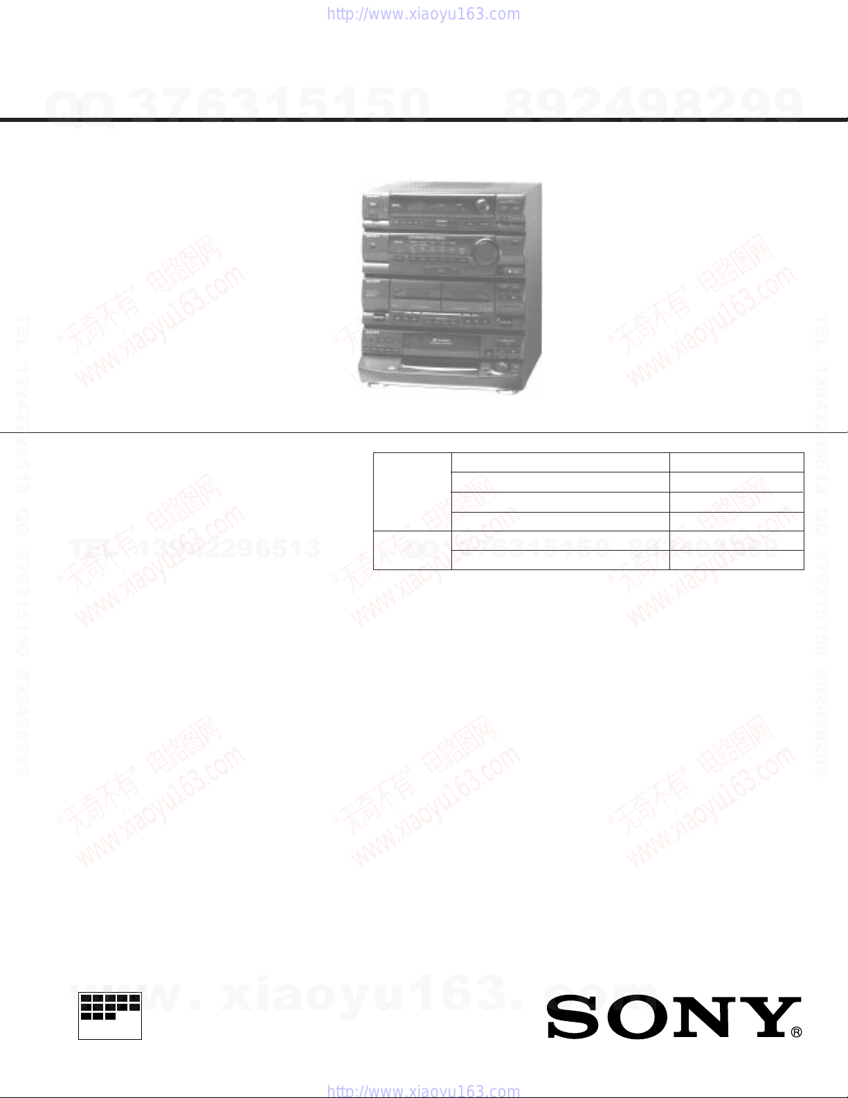
Photo: HCD-N555AV
Model Name Using Similar Mechanism NEW
CD
SECTION
T APE
DECK
Q
SECTION
CD Mechanism type CDM37-5BD19
Base Unit Type BU-5BD19
Optical Pick-up type KSS-213BA/S-N
Model Name Using Similar Mechanism HCD-N350
3
Q
T ape Transport Mechanism Type TCM-220WR2E
7
6
3
1
5
1
5
US Model
Canadian Model
HCD-D670AV
AEP Model
UK Model
E Model
Australian Model
PX Model
HCD-N555AV
2
8
9
4
2
9
8
0
9
TEL 13942296513 QQ 376315150 892498299
9
SPECIFICATIONS
AUDIO POWER SPECIFICATIONS (US model)
POWER OUTPUT AND T OTAL HARMONIC DISTORTION: W ith 6 ohm
loads, both channels driven, from 70-20,000 Hz; rated 50 watts per channel
minimum RMS power, with no more than 0.9 % total harmonic distortion
from 250 milliwatts to rated output (FRONT SPEAKER).
CD player section
System compact disc
digital audio system
Laser Semiconductor laser
(λ=780nm)
Emission duration:
continuous
laser output Max 44.6 µW*
* This output is the value measured at a distance of 200 mm from the objuctive
lens surface on the Optical Pick-up Block with 7 mm aperture.
Frequency response 2 Hz-20 kHz (± 0.5 dB)
wavelength 780-790 nm
T uner section
FM stereo, FM/AM superheterodyne tuner
FM tuner section
87.5-108.0 MHz
(100 kHz step for US, Canadian models)
(50 kHz step for except US, Canadian models)
Antenna FM wire antenna
Aerial terminals 75 ohm unbalanced
Intermediate frequency
10.7 MHz
AM tuner section
Tuning range
US, Canadian models:
AM: 530-1,710 kHz (with the tuning interval set at 10 kHz)
531-1,710 kHz (with the tuning interval se at 9 kHz)
German and Italian models:
AM: 531-1,602 kHz
AEP, UK models:
MW: 531-1,602 kHz
LW: 153-279 kHz (with the tuning inteval set at 3 kHz)
Other models:
AM: 531-1,602 kHz (with the AM tuning interval set at 9 kHz)
530-1,710 kHz (with the AM tuning interv al set at 10 kHz)
Antenna AM loop Antenna
External Antenna
terminals
Intermediate frequency
450 kHz
– Continued on next page –
COMPACT DISC DECK RECEIVER
w
w
MICROFILM
w
.
xia
o
y
u
1
6
— 1 —
3
.
c
o
m
7
Tape player section
Q
Q
Recording system
4-track 2-channel stereo
Frequency response
(DOLBY NR OFF)
40-13,000 Hz (±3 dB), using
SONY TYPE I cassette
40-14,000 Hz (±3 dB), using
SONY TYPE II cassette
Wow and flutter
± 0.15% W.Peak (IEC)
0.1% W .RMS (NAB)
± 0.2% W.Peak (DIN)
Amplifier section
TEL 13942296513 QQ 376315150 892498299
US, Canadian models:
Continuous RMS power output:
FRONT SPEAKER:
60 W + 60 W (6 ohms at 1 kHz, 5% THD)
CENTER SPEAKER:
50 W (8 ohms at 1 kHz, 5% THD)
REAR SPEAKER:
25 W + 25 W (16 ohms at 1 kHz, 5% THD)
AEP, UK, German, Italian models:
DIN power output:
FRONT SPEAKER:
40 W + 40 W(6 ohms at 1 kHz)
SUPER WOOFER:
40 W + 40 W (6 ohms)
SURROUND SPEAKER CENTER:
35 W (8 ohms at 1 kHz)
SURROUND SPEAKER REAR:
TEL
17.5 W + 17.5 W (16 ohms at 1 kHz)
Continuous RMS power output:
FRONT SPEAKER:
50 W + 50 W (6 ohms at 1 kHz, 10% THD)
SUPER WOOFER:
50 W + 50 W (6 ohms, 10% THD)
SURROUND SPEAKER CENTER:
42 W (8 ohms at 1 kHz, 10% THD)
SURROUND SPEAKER REAR:
21 W + 21 W (16 ohms at 1 kHz, 10% THD)
Music power output:
FRONT SPEAKER:
80 W + 80 W (6 ohms at 1 kHz, 10% THD)
SUPER WOOFER:
80 W + 80 W (6 ohms, 10% THD)
SURROUND SPEAKER CENTER:
70 W (8 ohms at 1 kHz, 10% THD)
SURROUND SPEAKER REAR:
35 W + 35 W(16 ohms at 1 kHz, 10% THD)
Other models:
Peak music power output:
1,400 W (6 Ω at 1 kHz, 10% THD)
Continuous RMS power output:
FRONT SPEAKER
45 W + 45 W (6 ohms, at 1 kHz, 5% THD)
SUPER WOOFER
45 W + 45 W (6 ohms, 5% THD)
SURROUND CENTER SPEAKER
40 W (8 ohms, at 1kHz 5% THD)
SURROUND REAR SPEAKER
20 W + 20 W (16 ohms, at 1 kHz, 5% THD)
3
13942296513
6
3
1
5
1
5
0
Inputs
PHONO (phono jack):
Sensitivity 3 mV, impedance 47 kilohms
VIDEO (AUDIO) (phono jack):
Sensitivity 250 mV, impedance 47 kilohms
MIC (phone jack): (E, Australian, Mexican, PX, Aregentine models)
Sensitivity 1 mV, impedance 10 kilohms
Outputs
PHONES (phone jack):
US, Canadian, AEP, UK, German, Italian models:
accept headphones of 8 ohms or more
Other models: accept headphones of 6 to 16 ohms
FRONT SPEAKER: accept impedance of 6 to 16 ohms
SURROUND SPEAKER REAR:
accept impedance of 16 ohms
SURROUND SPEAKER CENTER:
AEP, UK, German,Italian models:
accept impedance of 8 ohms
E, Australian, PX, Argentine, Mexican models:
accept impedance of 8 to 16 ohms
SUPER WOOFER:
AEP, UK, German, Italian models:
accept impedance of 16 ohms
E, Australian, PX, Argentine, Mexican models:
accept impedance of 6 to 16 ohms
General
Power requirements
AEP, UK, German, Italian, models:
220-230 V AC, 50/60 Hz
Australian model:
240 V AC, 50/60 Hz
7
3
Q
Q
US,Canadian, Mexican model:
120 V AC, 60 Hz
Other models:
110-120 V or 220-240 V AC
adjustable, 50/60 Hz
Power consumption
US model:170 W
Canadian model:190 W
AEP, UK, German, Italian models:250 W
Other models: 240W
Dimensions
Approx. 355 x 425 x 400 mm
(14 x 16 3/4 x15 3/4 inches) (w/h/d)
incl. projecting parts and controls
Mass
US, Canadian models:
Approx. 12.4 kg (27 lb 6 oz)
Except US, Canadian models:
Approx. 13 kg (28 lb11 oz)
Disegn and specifications subject to change withoutnotice.
6
8
3
9
1
5
1
2
5
4
0
9
8
9
8
2
4
2
9
8
9
2
9
9
TEL 13942296513 QQ 376315150 892498299
9
w
w
w
.
xia
o
y
u
1
6
— 2 —
3
.
c
o
m
7
Q
Q
TEL 13942296513 QQ 376315150 892498299
TEL
3
MODEL IDENTIFICATION
– BACK PANEL –
D670AV: US model
D670AV: Canadian model
N555AV : AEP model
N555AV: German model
N555AV: Italian model
N555AV: UK model
N555AV: E model
N555AV : Argentine model
N555AV : Australian model
13942296513
N555AV: PX model
N555AV: Mexican model
NOTE: The AEP model has lndonsian and Malaysia products.
The contents of both products are completely the same.
6
MODEL
3
Parts No.
1
5
1
PARTS No.
4-978-193-0π
4-978-193-1π
4-978-193-2π
4-978-193-3π
4-978-193-4π
4-978-193-5π
4-978-194-0π
4-978-194-1π
4-978-194-2π
4-978-194-3π
4-978-194-4π
5
0
Q
Q
Notes on chip component replacement
• Never reuse a disconnected chip component.
• Notice that the minus side of a tantalum capacitor may be
Flexible Circuit Board Repairing
• Keep the temperature of soldering iron around 270˚C
• Do not touch the soldering iron on the same conductor of the
• Be careful not to apply force on the conductor when soldering
Laser component in this product is capable of emitting radiation
exceeding the limit for Class 1.
7
3
4
2
9
8
damaged by heat.
during repairing.
circuit board (within 3 times).
or unsoldering.
CAUTION
Use of controls or adjustments or performance of
procedures other than those specified herein may result in
hazardous radiation exposure.
0
5
1
5
1
3
6
9
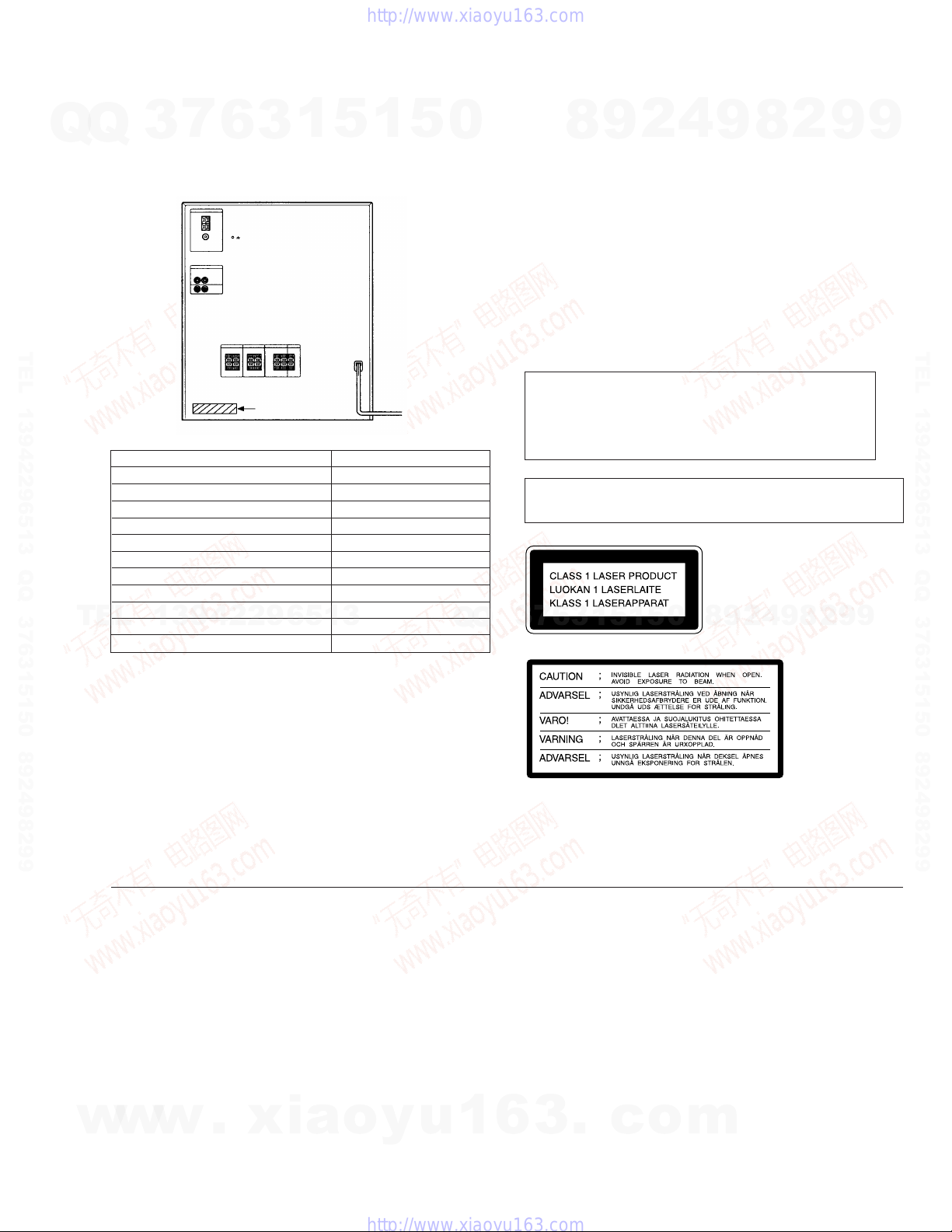
This appliance is classified as a
CLASS 1 LASER product.
The CLASS 1 LASER PRODUCT
MARKING is located on the rear
exterior.
2
9
8
8
4
2
9
2
8
9
This caution label
is located inside
the unit.
9
9
TEL 13942296513 QQ 376315150 892498299
9
w
w
SAFETY-RELATED COMPONENT WARNING !!
COMPONENTS IDENTIFIED BY MARK ! OR DO TTED LINE
WITH MARK ! ON THE SCHEMATIC DIAGRAMS AND IN
THE PARTS LIST ARE CRITICAL TO SAFE OPERATION.
REPLACE THESE COMPONENTS WITH SONY PARTS
WHOSE PART NUMBERS APPEAR AS SHOWN IN THIS
MANUAL OR IN SUPPLEMENTS PUBLISHED BY SONY.
w
.
xia
o
y
u
1
ATTENTION AU COMPOSANT AYANT RAPPORT
À LA SÉCURITÉ!!
LES COMPOSANTS IDENTIFIÉS P AR UNE MARQUE ! SUR
LES DIAGRAMMES SCHÉMATIQUES ET LA LISTE DES
PIÈCES SONT CRITIQUES POUR LA SÉCURITÉ DE
FONCTIONNEMENT. NE REMPLA CER CES COMPOSANTS
QUE P AR DES PIÈCES SONY DONT LES NUMÉROS SONT
DONNÉS DANS CE MANUEL OU DANS LES
SUPPLÉMENTS PUBLIÉS PAR SONY.
6
3
.
c
o
m
— 3 —
7
Q
Q
After correcting the original service problem, perform the following
safety checks before releasing the set to the customer:
Check the antenna terminals, metal trim, “metallized” knobs, screws,
and all other exposed metal parts for AC leakage. Check leakage as
described below.
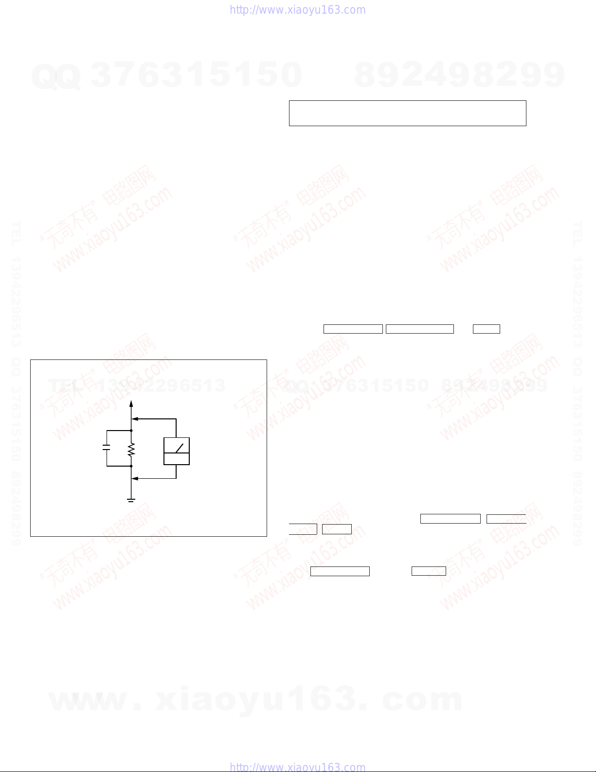
LEAKAGE
The AC leakage from any exposed metal part to earth ground and
from all exposed metal parts to any exposed metal part having a return
to chassis, must not exceed 0.5 mA (500 microampers). Leakage
current can be measured by any one of three methods.
TEL 13942296513 QQ 376315150 892498299
1. A commercial leakage tester, such as the Simpson 229 or RCA
WT-540A. Follow the manufacturers’ instructions to use these
instruments.
2. A battery-operated AC milliammeter. The Data Precision 245
digital multimeter is suitable for this job.
3. Measuring the voltage drop across a resistor by means of a V OM
or battery-operated AC voltmeter. The “limit” indication is 0.75
V, so analog meters must have an accurate low-voltage scale.
The Simpson 250 and Sanwa SH-63Trd are examples of a passi ve
VOM that is suitable. Nearly all battery operated digital
multimeters that have a 2V AC range are suitable. (See Fig. A)
TEL
Fig. A. Using an AC voltmeter to check AC leakage.
3
SAFETY CHECK-OUT
To Exposed Metal
13942296513
Parts on Set
0.15µF
6
1.5k
Ω
Earth Ground
3
1
AC
voltmeter
(0.75V)
5
1
5
0
NOTES ON HANDING THE OPTICAL PICK-UP BLOCK
OR BASE UNIT
The laser diode in the optical pick-up block may suffer electrostatic
break-down because of the potential difference generated by the
charged electrostatic load, etc. on clothing and the human body.
During repair, pay attention to electrostatic break-down and also use
the procedure in the printed matter which is included in the repair
parts.
The flexible board is easily damaged and should be handled with
care.
NOTES ON LASER DIODE EMISSION CHECK
The laser beam on this model is concentrated so as to be focused on
the disc reflective surface by the objecti ve lens in the optical pick-up
block. Therefore, when checking the laser diode emission, observe
from more than 30 cm away from the objective lens.
[FL Display Tube, LED All Lit and Key Check mode]
When the TUNER/BAND , DISPLAY/DEMO , and FILE 2 buttons
are pressed simultaneously, the FL display tube and LEDs will all
light up. Press any button to enter the key check mode.
When the key check mode is entered, the FL display tube displays
“K 1 J0 V0”. Each time a button is pressed, the counter increases in
the following order, K 2 n K 3 n K 4.
Q
Q
If buttons already pressed once are pressed again, the counter will
not increase. When the VOLUME knob is rotated in the + direction,
the count increases in the following order.
V1 n V2 n V3.
When rotated in the – direction, it decreases in the following order.
V0 n V9 n V8.
When the AMS dial is rotated in the clockwise direction, the count
increases in the following order.
J1 n J2 n J3.
When rotated in the counterclockwise direction, it decreases in the
following order.
J0 n J9 n J8.
To exit form the test mode, press the TUNER/BAND , DISPLAY/
DEMO , FILE 2 buttons simultaneously again.
3
7
9
8
SERVICING NOTE
1
5
1
3
6
2
5
4
0
9
8
9
8
2
4
2
9
8
9
2
9
9
TEL 13942296513 QQ 376315150 892498299
9
w
w
w
.
xia
[Switching the channel step 9 KHz/10 KHz]
Press ENTER/NEXT button and POWER button simultaneously
to switch the AM channel step 9 kHz and 10 kHz. Be sure not to
change with carelessness.
o
y
u
1
6
— 4 —
3
.
c
o
m
7
Q
Q
TEL 13942296513 QQ 376315150 892498299
TEL
3
Section Title Page
SECTION 1. GENERAL ...................................................... 6
SECTION 2. DISASSEMBLY
2-1. Front Panel Assy and Main Board ......................................... 8
2-2. TC Mechanism Deck ............................................................. 8
2-3. CD Mechanism Deck ............................................................. 9
2-4. BU Bracket Assy.................................................................... 9
2-5. Disc Table ............................................................................ 10
SECTION 3. MECHANICAL ADJUSTMENTS......... 11
SECTION 4. ELECTRICAL ADJUSTMENTS
DECK Section ............................................................................. 11
TUNER Section........................................................................... 14
CD Section................................................................................... 15
SECTION 5. DIAGRAMS
5-1. Circuit boards location ........................................................ 17
5-2. IC Pin Functions .................................................................. 18
• IC501 Graphic Control (ASD0204) .................................. 18
• IC701 Master Control (TMP87CS64YF) .......................... 19
5-3. Block Diagrams
• Main Section...................................................................... 22
13942296513
• Tuner Section
(US, CND, E, AUS, MX, PX, AR Model)......................... 25
• Tuner Section
(AEP, UK, G, IT Model) .................................................... 27
• DECK Section ................................................................... 29
• CD Section......................................................................... 31
5-4. Schematic Diagram — Tuner Section —
(US, CND, E, AUS, MX, PX, AR Model)........................... 34
5-5. Printed Wiring Board — Tuner Section —
(US, CND, E, AUS, MX, PX, AR Model)........................... 36
5-6. Schematic Diagram — Tuner Section —
(AEP, UK, G, IT Model) ..................................................... 38
5-7. Printed Wiring Board — Tuner Section —
(AEP, UK, G, IT Model) ..................................................... 40
5-8. Schematic Diagram — CD Panel Section — ...................... 41
5-9. Printed Wiring Board — CD Panel Section —.................... 42
5-10. Schematic Diagram — CD Section — .............................. 45
5-11. Printed Wiring Board — CD Section —............................ 47
5-12. Printed Wiring Board — Deck Section — ......................... 49
5-13. Schematic Diagram — Deck Section —............................ 51
5-14. Printed Wiring Board — Main Section —......................... 57
5-15. Schematic Diagram — Main Section —............................ 59
5-16. Schematic Diagram — Panel Section — ........................... 64
5-17. Printed Wiring Board — Panel Section — ........................ 69
5-18. Printed Wiring Board — Power Section — ....................... 73
5-19. Schematic Diagram — Power Section —.......................... 77
5-20. Schematic Diagram — CD Motor Section — ................... 80
5-21. Printed Wiring Board — CD Motor Section —................. 81
5-22. IC Block Diagrams — CD Section — ............................... 83
6
TABLE OF CONTEMTS
3
1
5
1
5
0
Q
Q
Section Title Page
SECTION 6. EXPLODED VIEWS
6-1. Case and Back Panel Section ............................................... 85
6-2. Panel Board Section ............................................................. 86
6-3. Front panel Section .............................................................. 87
6-4. Chassis Section .................................................................... 88
6-5. TC Mechanism Section 1 (TCM-220WR2E) ...................... 89
6-6. TC Mechanism Section 2 (TCM-220WR2E) ...................... 90
6-7. TC Mechanism Section 3 (TCM-220WR2E) ...................... 91
6-8. CD Mechanism Section(CDM37-5BD19)........................... 92
6-9. Base Unit Section (BU-5BD19)........................................... 93
SECTION 7. ELECTRICAL PARTS LIST ................... 94
• Abbreviation
7
3
2
9
8
G : German model
IT : Italian model
MX : Mexican model
AUS: Australian model
AR : Argentine model
5
1
5
1
3
6
4
0
9
8
9
8
2
4
2
9
8
9
2
9
9
TEL 13942296513 QQ 376315150 892498299
9
w
w
w
.
xia
o
y
u
1
6
— 5 —
3
.
c
o
m
SECTION 1
GENERAL
7
Q
Q
TEL 13942296513 QQ 376315150 892498299
3
*1
6
3
1
5
1
5
*3
0
*3
This section is extracted from
instruction manual.
2
9
8
FM 75Ω COAXIAL terminal
4
9
*5
8
*1
2
9
9
TEL 13942296513 QQ 376315150 892498299
TEL
13942296513
DOLBY NR button
*6
9
9
2
8
9
4
2
9
8
0
5
1
5
1
3
6
7
3
Q
Q
*4
Note:
*1 : AEP, UK, German, Italian models.
*2 : Except US, Canadian models.
*3 : E, Australian, Mexican, PX,
Argentine models
*4 : US, Canadian, AEP, UK,
German, Italian models.
*5 : Except AEP, UK, German,
Italian models.
*6 : E, PX, Argentine models.
*2
KARAOKE PON/MPX button
w
w
w
.
*2
*3
xia
o
y
u
1
6
— 6 —
3
.
c
o
m
7
Q
Q
TEL 13942296513 QQ 376315150 892498299
3
6
3
1
5
1
5
0
8
9
2
4
9
8
2
9
9
TEL 13942296513 QQ 376315150 892498299
TEL
13942296513
*3
DOLBY NR B indication
*4
Q
Q
3
7
6
3
1
5
1
5
0
8
9
2
4
9
8
2
9
9
w
w
w
.
xia
o
y
u
1
6
— 7 —
3
.
c
o
m
SECTION 2
DISASSEMBLY
Note: Follow the disassembly procedure in the numerical order given.
Q
Q
2-1. FRONT PANEL ASSY AND MAIN BOARD
1
Remove the connectors.
• Main board (six connectors)
• Main power amplifier board (one connector)
3
3
7
6
2
Screw (BVTP3 X 8)
Two earth wire
3
1
5
CN1301
1
5
0
9
8
6
Screw (BVTP 3x8)
2
4
9
8
2
9
9
TEL 13942296513 QQ 376315150 892498299
CN402
Power amp board
CN401
CN701
Q
CN203
3
7
5
Front panel assy
TEL
2-2. TC MECHANISM DECK
13942296513
4
Three screws
(BVTP 3X8)
6
Button (eject-L)
Q
3
Three screws
(BVTP 2.6X8)
CN201
3
6
CN250
5
1
8
Main board
0
5
1
4
Four screws
(BVTP 2.6X8)
7
Two scrws
(BVTP 3X8)
9
8
2
4
9
8
2
9
TEL 13942296513 QQ 376315150 892498299
9
w
w
2
Remove the two cassette lids
direction of arrow.
w
.
xia
o
y
u
1
6
— 8 —
5
6
Button (eject-R)
3
.
c
1
Push the eject button.
TC mechanism deck
o
m
Q
TEL 13942296513 QQ 376315150 892498299
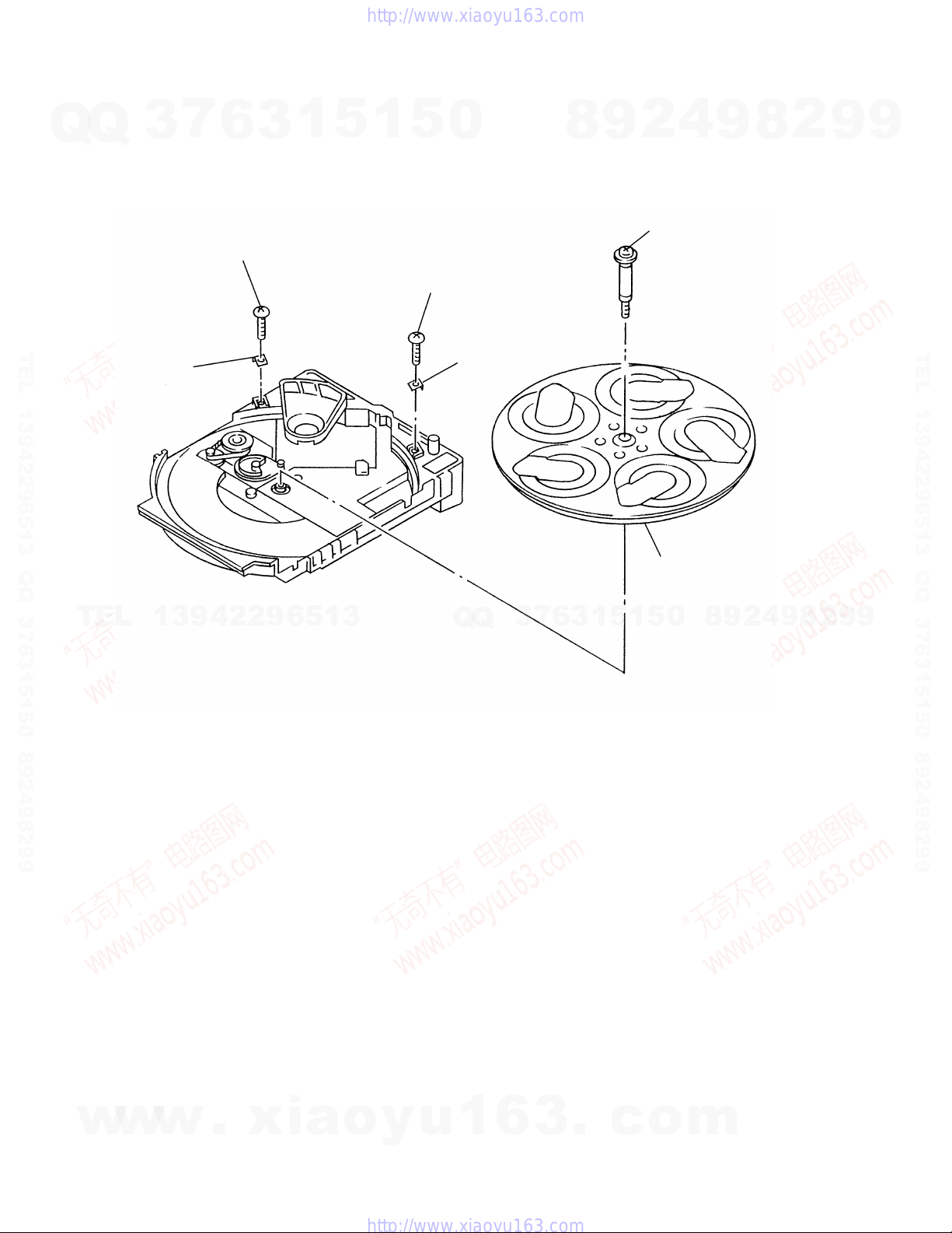
2-3. CD MECHANISM DECK
Q
3
7
6
1
3
2
Two screws
(BVTP 3X8)
5
1
5
1
0
Screw (BVTP 3X8)
9
8
3
Two screws
(BVTP 3X8)
4
2
4
CD mechanism deck
9
8
2
9
9
TEL 13942296513 QQ 376315150 892498299
TEL
13942296513
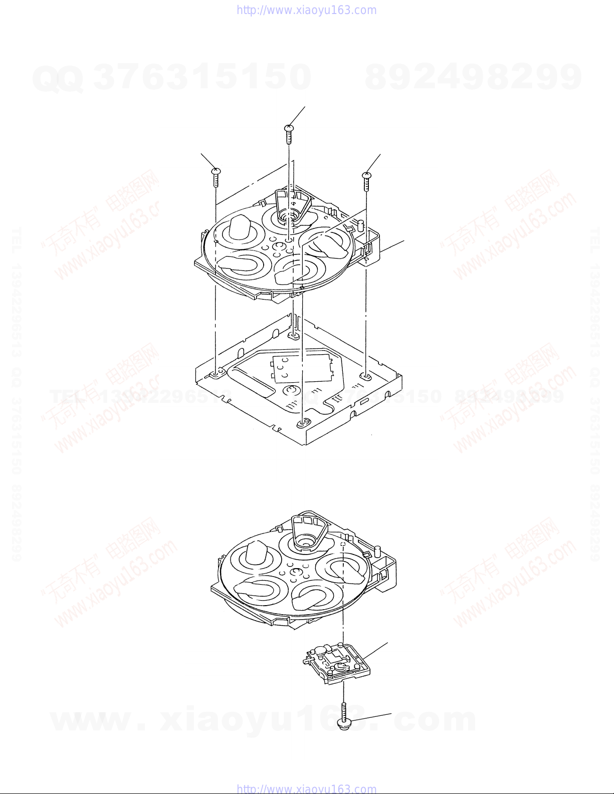
2-4. BU BRACKET ASSY
Q
Q
3
7
6
3
1
5
1
5
2
BU bracket assy
0
8
9
2
4
9
8
2
9
9
w
w
w
.
xia
o
y
u
1
6
— 9 —
3
.
1
Yoke bracket
c
o
m
7
Q
Q
2-5. DISC TABLE
TEL 13942296513 QQ 376315150 892498299
3
2
Bracket (BU)
6
1
Screw (BVTP 3X8)
3
1
5
1
5
3
Screw (BVTP 3X8)
0
4
Bracket (BU)
8
9
2
5
Step screw
6
4
Disc table
9
8
2
9
9
TEL 13942296513 QQ 376315150 892498299
TEL
13942296513
Q
Q
3
7
6
3
1
5
1
5
0
8
9
2
4
9
8
2
9
9
w
w
w
.
xia
o
y
u
1
6
— 10 —
3
.
c
o
m

SECTION 3
MECHANICAL ADJUSTMENTS
7
Q
Q
TEL 13942296513 QQ 376315150 892498299
TEL
3
1. Clean the following parts with a denatured alcohol-moistened
swab :
record/playback heads pinch rollers
erase head rubber belts
capstan idlers
2. Demagnetize the record/playback head with a head demagnetizer .
3. Do not use a magnetized screwdriver for the adjustments.
4. The adjustments should be performed with the rated power supply
voltage unless otherwise noted.
Torque Measurement
Torque
FWD
FWD
back tension
REV
REV
back tension
FF/REW
FWD tension
REV tension
13942296513
6
1
3
PRECAUTION
Torque meter
CQ-102C
CQ-102C
CQ-102RC
CQ-102RC
CQ-201B
CQ-403A
CQ-403R
5
1
5
0
Meter reading
36 to 61g • cm
(0.5–0.84 oz • inch)
2 to 6g • cm
(0.02–0.08 oz • inch)
36 to 61g • cm
(0.5–0.84 oz • inch)
2 to 6g • cm
(0.02–0.08 oz • inch)
61 to 143g • cm
(0.85–1.99 oz • inch)
100g or more
(3.53 oz or more)
100g or more
(3.53 oz or more)
Q
Q
DECK SECTION 0 dB=0.775V
1. Demagnetize the record/playback head with a head damagnetizer .
2. Do not use a magnetized screwdriver for the adjustments.
3. After the adjustments, apply suitable locking compound to the
4. The adjustmetns should be performed with the rated power supply
5. The adjustments should be performed in the order given in this
6. The adjustments should be performed for both L-CH and R-ch.
7. Switches and controls should be set as follows unless otherwise
Record/Playback Head Azimuth Adjustment
DECK A DECK B
Note : Perform this adjustments for both decks.
7
3
Procedure :
1. Mode : Playback (FWD)
SECTION 4
ELECTRICAL ADJUSTMENTS
4
2
9
8
parts adjusted.
voltage unless otherwise noted.
service manual. (As a general rule, playback circuit adjustment
should be completed before performing recording circuit
adjustment.)
specified.
DOLBY NR switch : OFF (US, CND, AEP, UK, G, IT model)
Tape
P-4-A100
WS-48B
P-4-L300
0
5
1
5
1
3
6
9
Signal
10 kHz, –10 dB
3 kHz, 0 dB
315 Hz, 0 dB
9
8
2
2
8
Tape Speed Adjustment
9
4
9
Used for
Azimuth Adjustment
Level Adjustment
2
8
9
9
9
TEL 13942296513 QQ 376315150 892498299
w
w
w
.
xia
o
y
u
1
test tape
P-4-A100
(10kHz, –10dB)
• Abbreviation
CND : Canadian model.
G : German model.
IT : Italian model.
6
3
.
c
set
o
main board
CN403
3
(L-CH)
Pin
Pin 1 (R-CH)
main board
CN403
Pin
2
m
level meter
— 11 —
7
Q
Q
2. Turn the adjustment screw and check output peaks. If the peaks
do not match for L-CH and R-CH, turn the adjustment screw so
that outputs match within 1 dB of peak.
L-CH
peak
TEL 13942296513 QQ 376315150 892498299
screw
position
3. Mode : Playback (FWD)
test tape
P-4-A100
(10kHz, –10dB)
TEL
3
output
level
R-CH
peak
13942296513
6
within
1dB
L-CH
peak
main board
CN403
Pin
L
set
R
3
3
Pin
1
2
R-CH
peak
5
1
within 1dB
oscilloscope
screw
position
5
0
Tape Speed Adjustment DECK A
NOTE : Start the tape speed adjustment as bellow after setting the
test mode.The tape speed can be changed with the HIGH
SPEED DUBBING button during the test mode.
Method :
1. Turn the power switch on.
2. Press the DISPLAY/DEMO button, MENU 1 button and TUNER/
BAND button simulateously.
Procedure :
Mode : Playback (FWD)
test tape
WS-48B
(3kHz, 0dB)
1. Insert tha WS-48B into the deck A to playback.
2. Press the HIGH SPEED DUBBING button. Then at HIGH
SPEED mode.
3. Adjust RV652 on the MD board so that the frequency counter
reading becomes 6,000 ± 30 Hz.
4. Press the HIGH SPEED DUBBING button again to be set the
NORMAL SPEED mode.
Q
Q
5. Set to the playback mode.
6. Adjust RV651 on the MD board so that the frequency counter
reading becomes 3,000 ± 15 Hz.
3
7
6
9
8
set
main board
CN403 (Pin 3 : L-CH)
5
1
3
2
(Pin 1 : R-CH)
0
5
1
4
9
frequency counter
9
8
8
2
4
2
9
8
9
2
9
9
TEL 13942296513 QQ 376315150 892498299
9
Pin
1
Waveform of oscilloscope
in phase
4. Repeat steps 1 to 3 in playback (REV) mode.
5. After the adjustments, apply suitable locking compound to the
parts adjusted.
Adjustment Location : Record/Playback Head (Deck A and B)
FWD side
w
w
w
45
°
90
good
REV side
Adjustment screw
.
xia
°
135
°
180
°
wrong
o
y
Frequency difference between deck A and deck B the beginning of
the tape should be within ± 1.5%.
Adjustment Location : MD board
Playback Level Adjustment DECK A DECK B
Procedure :
Mode : Playback (FWD)
test tape
P-4-L300
(315Hz, 0dB)
set
main board
CN403 (Pin
(Pin 1 : R-CH)
Deck A is RV311 (L-CH) and RV411 (R-CH), deck B is RV301 (LCH) and RV401 (R-CH) so that adjustment within the following
adjustment level.
Adjustment level :
CN403 PB level : 301.5 to 338.3 mV (–8.2 to –7.2 dB)
level difference between the channels : within ± 0.5 dB
Adjustment Location : MD board
u
1
6
3
.
c
o
3
: L-CH)
m
level meter
— 12 —
7
Q
Q
TEL 13942296513 QQ 376315150 892498299
TEL
3
Record Bias Current Adjustment DECK B
Procedure :
1. Mode : record
AF OSC
2. Mode : Playback
Confirm playback the signal recorded in step 1 become adjustment
level as follows.
If these levels do not adjustment level, adjust the RV341 (L-CH) and
13942296513
RV441 (R-CH) on the MD board to repeat step 1 and 2.
6
attenuator
recorded
position
set
3
600
CN 403 (Pin
1
VIDEO IN
1) 315Hz
2) 10kHz
Ω
5
1
50mV (–23.8dB)
set
3
: L-CH)
(Pin 1 : R-CH)
5
blank tape
CS-123
level meter
0
Q
Q
2. Mode : Playback
Confirm playback the signal recorded in step 1 become adjustment
level as follows.
If these levels do not adjustment level, adjust the RV301 (L-CH) and
RV351 (R-CH) on the main board to repeat steps 1 and 2.
Adjustment level: CN 403 PB level: 47.2 to 53.0 mV
Adjustment Location : main board
Adjustment Location
[MAIN BOARD] (Component Side)
7
3
6
8
3
9
recorded
position
5
1
4
2
set
main board
CN403 (Pin
(–24.3 to –23.3 dB)
1
3
CN403
8
0
5
1
2
8
9
level meter
3
: L-CH)
(Pin 1 : R-CH)
RV351 REC LEVEL (R-CH)
2
8
9
4
2
9
RV301 REC LEVEL
(L-CH)
9
9
9
TEL 13942296513 QQ 376315150 892498299
9
Adjustment level : The playback output of 10 kHz level difference
against 315Hz reference should be ± 0.5 dB
Adjustment Location : MD board
Record Level Adjustment DECK B
Procedure :
1. Mode : record
VIDEO IN
315Hz, 50mV (–23.8dB)
AF OSC
attenuator
600
Ω
set
blank tape
CS-123
[MD BOARD] (Conductor Side)
RECORD
BIAS
¬
RV301
RV401¬R
PB LEVEL
– DECK B –
R
L
RV441
L
RV341
TAPE SPEED
(NORMAL)
RV651
¬
PB
LEVEL
– DECK A –
L
R
(HIGH)
RV652
¬
¬
¬
w
w
w
.
xia
o
y
u
1
6
— 13 —
3
.
c
o
m
7
Q
Q
TUNER SECTION 0dB=1µV
Note : As a front-end (FE1) is difficult to repair if faulty, replace it
with new one.
AM Tuned Level Adjustment
Note : FM Tuned Level adjustment should be performed after this
AM Tuned Level adjustment.
Setting :
Band : AM or MW
TEL 13942296513 QQ 376315150 892498299
Carrier frequency : 999kHz (at 9kHz step)
Procedure :
1. Set the output of SGG so that the input level of the set becomes 55
dB.
2. Tune the set to 999 kHz or 1050 kHz .
3. Adjust RV41 (AEP, UK, IT, G models), RV42 (other models) to
the point (moment) when the TUNED indicator will change from
TEL
going off to going on.
3
AM RF SSG
30% amplitude
modulation by
400 Hz signal
1050kHz (at 10 kHz step)
13942296513
6
3
1
5
1
loop antenna
5
0
60 cm
Field strength dB (
• Abbreviation
G : German model
IT : Italian model
loop antenna
(Supplied accessories)
µ
Adjustment Location
AEP, UK, G, IT model
[TCB BOARD] (Component Side)
7
3
Q
Q
4
2
9
8
AM antenna
terminal (TM1)
V/m)=SGG output level dB (µV/m)–26dB.
6
3
1
IC41
5
AM T uned Level
5
1
0
9
RV41
8
9
8
2
4
2
9
8
9
2
9
9
TEL 13942296513 QQ 376315150 892498299
9
Adjustment Location : TCB board
FM Tuned Level Adjustment
Note : This adjustment should be performed after the AM Tuned
Level Adjustement.
Setting :
Band : FM
FM RF stereo signal
generator
75
Ω
coaxial
set
Carrier frequency : 98MHz
Modulation : AUDIO 1kHz, 75kHz
Output level : 25dB (at 75
Procedure :
1. Supply a 25dB 98 MHz signal from the ANTENNA terminal.
2. Tune the set to 98 MHz.
3. Adjust RV42 (AEP, UK, IT, G models), RV41 (other models) to
the point (moment) when the TUNED indicator will change from
going off to going on.
w
Adjustment Location : TCB board
deviation (100%)
w
w
Ω
open)
.
FM ANTENNA terminal
(TM1) (75
Ω
)
xia
o
y
RV42
FM T uned Level
Other model
[TCB BOARD] (Component Side)
RV41
FM T uned Lev el
u
1
6
3
.
c
FE1
IC2
o
FE1
TM1
RV42
AM T uned
Level
TM1
m
— 14 —
7
3
Q
TEL 13942296513 QQ 376315150 892498299
CD SECTION
Q
Note :
1. CD Block is basically designed to operate without adjustment.
Therefore, check each item in order given.
2. Use YEDS-18 disc (3-702-101-01) unless otherwise indicated.
3. Use an oscilloscope with more than 10MΩ impedance.
4. Clean the object lens by an applicatior with neutral detergent when
the signal level is low than specified value with the following
checks.
5. Adjust the focus bias adjustment when optical block is replaced.
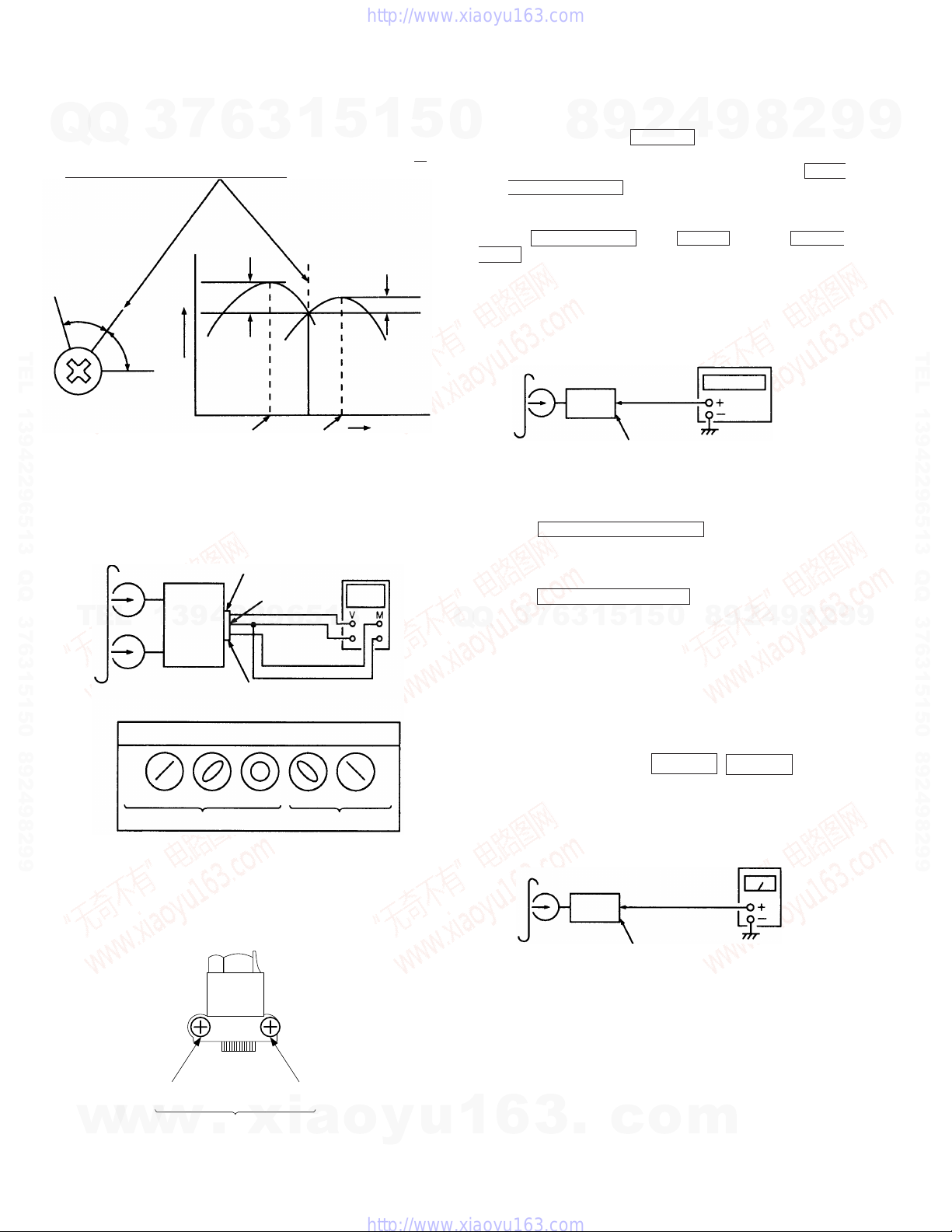
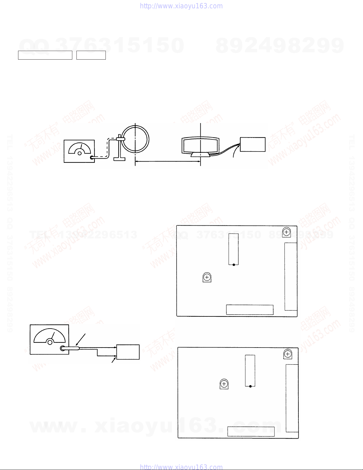
Focus Bias Adjustment
Procedure :
1. Connect oscilloscope to test point TP (RF).
(Ground terminal : VC)
2. Turned Power switch on.
3. Put disc (YEDS-18) in and playback.
4. Adjust RV101 so that the waveform is clear.
(Clear RF signal waveform means that the shape “◊ ” can be clearly
TEL
distinguished at the center of the waveform.)
13942296513
5. After adjustment, check the RF signal level.
• RF signal
VOLT/DIV : 200 mV
TIME/DIV : 500 nS
6
BD board
TP(RF)
TP(VC)
3
1
oscilloscope
(DC range)
5
1
5
0
Q
Q
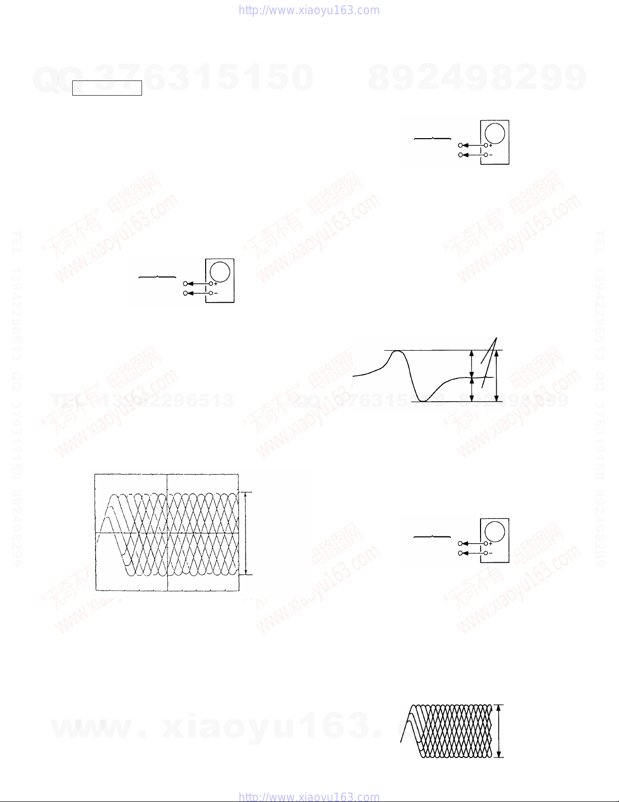
S Curve Check
Procedure :
1. Connect oscilloscope to test point TP (FEO).
2. Connect between test point TP (FOK) and Ground by lead wire.
3. Turn Power switch on.
4. Put disc (YEDS-18) in and turned Power switch on again and
5. Check the oscilloscope waveform (S-curve) is symmetrical
S-curve waveform
7
3
6. After check, remove the lead wire connected in step 2.
Note : • Try to measure several times to make sure than the ratio of
4
2
9
8
BD board
TP(FE)
TP(VC)
actuate the focus search. (actuate the focus search when disc table
is moving in and out.)
between A and B. And conf irm peak to peak lev el within 2.4 ± 0.7
Vp-p.
0
5
1
5
1
3
6
A : B or B :A is more than 10 :7.
• Take sweep time as long as possible and light up the
brightness to obtain best waveform.
9
8
9
oscilloscope
Symmetry
2
8
within 2.4
4
2
9
8
9
±
0.7 Vp-p
9
2
9
9
TEL 13942296513 QQ 376315150 892498299
w
w
w
.
xia
o
level
1.3 ± 0.3 Vp-p
y
u
1
RF Level Check
oscilloscope
BD board
TP(RF)
TP(VC)
Procedure :
1. Connect oscilloscope to test point TP (RF) on BD board.
2. Turned Power switch on.
3. Put disc (YEDS-18) in and playback.
4. Confirm that osilloscope waveform is clear and check RF signal
level is correct or not.
Note :
Clear RF signal waveform means that the shape “◊” can be clearly
distinguished at the center of the waveform.
RF signal waveform
VOLT/DIV : 200mV
TIME/DIV : 500nS
6
3
.
c
o
m
level : 1.3
±
0.3 Vp-p
— 15 —
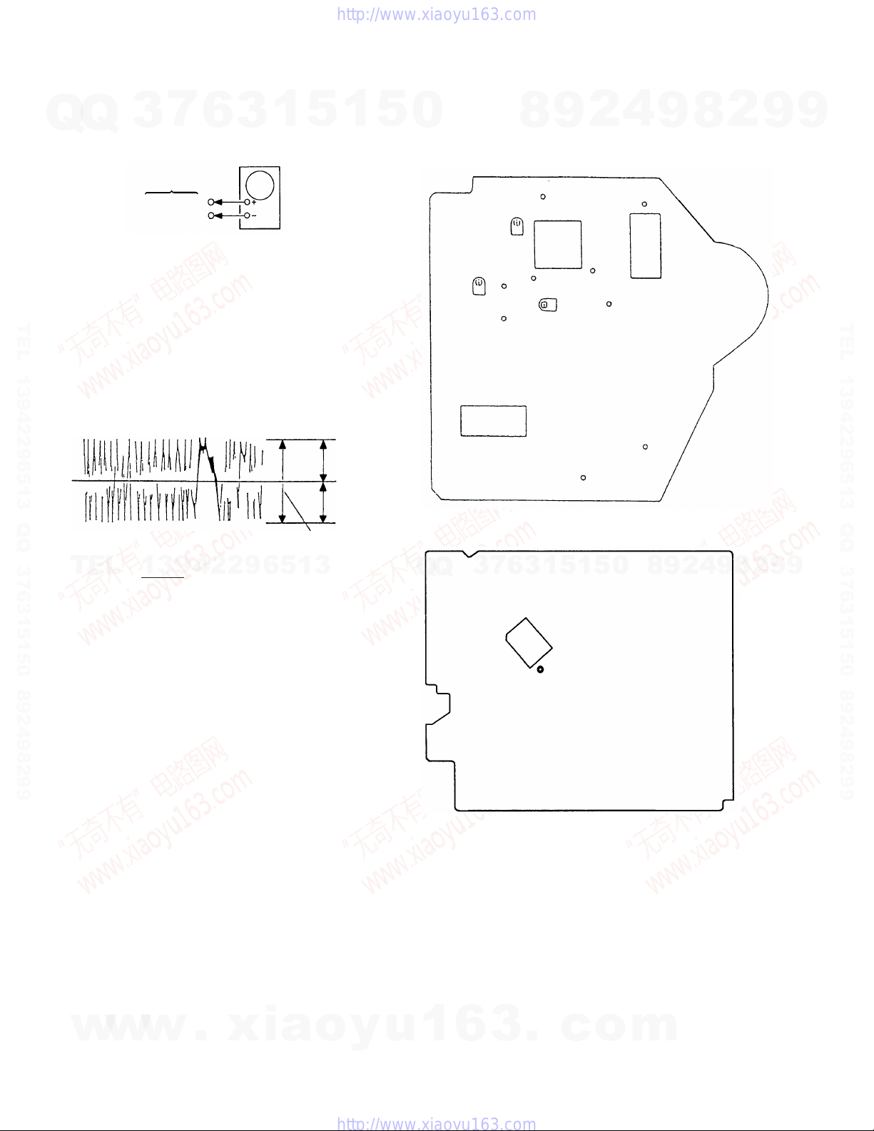
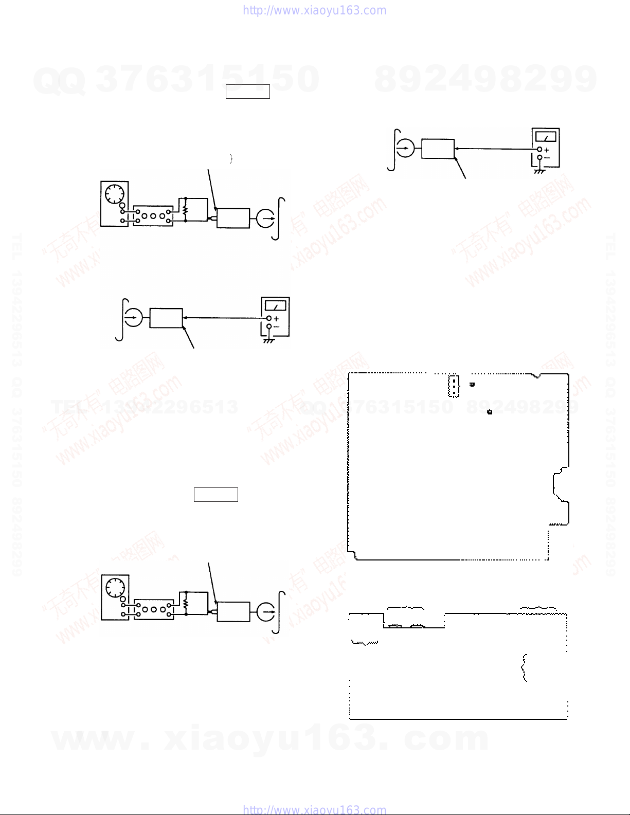
E-F Balance Check
Q
Q
Procedure :
1. Connect test point TP (ADJ) on Main board to Ground with a lead
wire.
2. Connect oscilloscope to test point TP (TEO).
TEL 13942296513 QQ 376315150 892498299
3. Turned Power switch on.
4. Put disc (YEDS-18) in and playback.
5. Confirm that the oscilloscope waveform is symmetrical on the
top and bottom in relation to 0Vdc, and check this level.
Traverse waveform
0V
3
BD board
TP (TEO)
7
TP (VC)
6
1
3
oscilloscope
level : 300 ± 100 mVp-p
5
A
B
1
5
Adjustment Location :
0
[BD BOARD] (Conductor Side)
RV103
IC104
[MAIN BOARD] (Conductor Side)
TEO
VC
8
RV101
9
RF
IC101
FEO
RV102
GND
2
TEI
FEI
4
FOK
PCK
9
IC102
8
2
9
9
TEL 13942296513 QQ 376315150 892498299
TEL
Specified level : • X 100=less than ± 7%
6. Remove the lead wire connected in step 1.
Focus/Tracking Gain Adjustment (RV102, RV103)
This gain has a margin, so even if it is slightly off.
There is no problem.
Therfore, do not perform this adjustment.
Please note that it should be fixed to mechanical center position when
you moved and do not know original position.
13942296513
A-B
2(A+B)
• A+B=300 ± 100 mVp-p
Q
Q
3
7
6
IC701
3
TP701
(ADJ)
1
5
1
5
0
8
9
2
4
9
8
2
9
9
w
w
w
.
xia
o
y
u
1
6
— 16 —
3
.
c
o
m
Q
7
Q
3
5-1. CIRCUIT BOARDS LOCATION
• Abbreviation
MX: Mexican model
AUS: Australian model
AR: Argentine model
6
3
1
SECTION 5
DIAGRAMS
5
1
5
0
TRANS board
PANEL board
8
2
9
S. WOOFER board
4
9
8
2
9
9
HP board
TEL 13942296513 QQ 376315150 892498299
MIC board
(E,AUS,MX,PX,AR)
CD LED board
CD (L) board
TC CONTROL board
TEL
13942296513
Note: rA is including in MD board.
DOOR SW board
r
A MOTOR board
Q
Q
7
3
CD JOG board
1
3
6
CD (R) board
MD board (including rA)
5
MAIN board
5
1
TCB board
POWER AMP board
9
8
0
2
4
9
8
2
9
TEL 13942296513 QQ 376315150 892498299
9
w
w
w
LEAF SWITCH board
TABLE SENSOR board
.
xia
o
y
u
1
6
CD MOTOR board
— 17 —
3
.
LED board
c
o
BD board
m
5-2. IC PIN FUNCTIONS
Q
Q
• IC501 GRAPHIC CONTROL (ASD0204)
Pin No.
1
VDD
2
LED8
3, 4
5-9
10
11
12
TEL 13942296513 QQ 376315150 892498299
13
14
15
16
17, 18
19
20
21
22
23
24
25
26-29
30-33
34
35
36
37
38
39
40
41
42
43-45
46
47, 48
49, 50
51-53
54-78
79
80-86
87-100
TEL
LDE7, 6
LED5–1
RESET
X2
X1
IC (Vpp)
XT2
JOG B
VDD
LED10, 9
KEY SEL
VOL B
REQ. GM
CLK MG
DATA GM
DATA MG
AVSS
SPEANA 4–1
KEY 4–1
AVDD
AVREF
VOL A
JOG A
RDY MG
SIRCS
VSS
DOR SW
LED SELECT
LED13–11
VDD
LEDS7, 6
LEDS5, 4
LEDS3–1
SEG32–8
V, LOAD
SEG7–1
GR14–1
7
3
6
13942296513
3
1
I/OPin Name
+5V
–
LED drive signal output.
O
LED drive signal output.
O
LED drive signal output.
O
Reset signal input.
I
O
X’ tal (4 MHz).
I
GND
–
Not used.
I
AMS encoder signal input.
I
+5V
–
LED drive signal output.
O
Key select control.
O
Volume encoder signal input.
I
Request signal from/to master control.
O
Serial clock input.
I
Serial data output.
O
Serial data input.
I
GND
–
Spectram analizer signal input.
I
Key matrix input.
I
–
+5V
–
Volume encoder signal input.
I
AMS encoder signal input.
I
Ready signal from master control.
I
SIRCS signal input.
I
GND
–
CD door open detection input.
I
LED select signal output.
O
LED drive signal output.
O
+5V
–
Not used.
O
Not used. (Pull down)
O
LED drive signal output.
O
FL segment signal output.
O
–25V for FL
–
FL segment signal output.
O
FL grid signal output.
O
5
1
5
0
Q
Q
3
7
8
Function
3
6
9
1
5
1
2
5
4
0
9
8
9
8
2
4
2
9
8
9
2
9
9
TEL 13942296513 QQ 376315150 892498299
9
• Abbreviation
FL: Fluorescent Indicator Tube
GND: Ground
w
w
w
.
xia
o
y
u
1
6
— 18 —
3
.
c
o
m
Q
TEL 13942296513 QQ 376315150 892498299
• IC701 MASTER CONTROL (TMP87CS64YF)
Q
Pin No.
TEL
7
3
1
2
3
4
5
6
7
8
9
10
11
12
13
14
15
16
17
18
19
20
21
22
23
24
25
26
13942296513
27
28
29
30
31
32
33
34
35
36
37
38
39
40
6
Pin Name
VSS
XOUT
XIN
RESET
XOUT
XIN
GND (test)
AC CUT
SUPER WOOFER ON
ST-MUTE ON
180-A-PLAY
180-B-PLAY
180-B-REC
V. DET
BD-UP (5CD)
TRAY CLOSE (1CD)
ENCODER-1
ENCODER-2
ENCODER-3
OUT SW OPEN
LOAD IN
LOAD OUT
TBL-L
TBL-R
SCOR
TBL-SENS
RDS INT
RDS DATA
DF LAT
SENS
XRST
MG-RDY
ADJ
GM-REQ
MG-CLK
GM-DATA
MG-DATA
CD-CLK
ADJ-2
CD-DATA
3
1
5
I/O
–
O
I
I
O
I
–
I
O
O
I
I
I
I
I
I
I
I
I
I
O
O
O
O
I
I
I
I
O
I
O
O
I
I
O
I
O
O
I
O
1
5
0
GND
X’ tal (10 MHz).
Reset signal input.
X’ tal for clock (32.768 kHz)
GND
Back up signal input.
Super woofer ON/OFF control.
Mute signal output for tuner.
Tape detection sigal input. (Connected to GND)
Voltage detection (Not used).
Disc table up detect.
Connected to GND
Input selector control signal output. (Pull up)
Out switch signal input. (Pull up)
Loading motor control signal output. (Not used)
Table motor control signal output.
Sub-code sync signal input.
CD Table sensor signal input.
RDS data start input.
RDS data output.
Latch signal for digital filter.
Table sence signal input.
Reset signal output for CD.
Ready signal to graphic control.
Test mode input.
Request signal from graphic control.
Clock signal to graphic control.
Data input from graphic control.
Data output to graphic control.
Clock output. Serial bus line.
Test mode input.
Data output. Serial bus line.
Q
Q
3
7
6
8
3
9
Function
5
1
1
2
5
4
0
9
8
9
8
2
4
2
9
8
9
2
9
9
TEL 13942296513 QQ 376315150 892498299
9
• Abbreviation
FL : Fluorescent Indicator Tube
GND : Ground
w
w
w
.
xia
o
y
u
1
6
— 19 —
3
.
c
o
m
7
Q
Q
Pin No.
41
42
43
44
45
46
47
48
49
50
TEL 13942296513 QQ 376315150 892498299
51
52
53
54
55
56
57
58
59
60
61
62
63
64
65
66
67
68
TEL
69
70
71
72
73
74
75
76
77
78
79
80
3
AUB IN
AUB OUT
FOCUS SW
SQ-CLK
SQ-DATA
X-LAT
TEST
VAREF
SS
AV
VSS
VDD
SPEC
DESTINATION
DISC SENS
TC RELAY
A-SHUT
B-SHUT
B-HALF
A-HALF
220-A-PLAY
220-B-PLAY
62427 LAT
K-CON-LAT
VOL LAT (AV)
FRONT SP RELAY B
REAR SP RELAY C
POWER ON
CD POWER
13942296513
RPOLOG LAT
MUTE
COM CLK
COM DIN
COM DATA
K CON ON
LIDDED LED
MD/VIDEO
DBFB-HIGH
PWM-OUT
PRO-LOGIC
TC A
6
3
I/OPin Name
1
5
1
5
0
I
Audio bus in/output. (Not used)
O
Focus switching signal output.
O
Subcode Q data read clock output.
O
Subcode Q data input.
I
Latch signal digital signal processor.
O
Test land.
I
Analog reference voltage input.
I
–
GND
–
+5V
–
I
Destination detection input.
I
Not used.
I
REC/PB select signal output.
O
I
I
I
Control signal input form deck.
I
I
I
PLL latch output.
O
Not used.
O
Latch signal for electrical volume. (Not used)
O
Not used.
O
Rear speaker relay control output.
O
Power on signal output
O
CD power control signal output.
O
Not used.
O
Mute signal for AMP.
O
PLL clock output. (PLL, Function, Graphic Equalizer)
O
PLL data input. (PLL, Function, Graphic Equalizer)
I
PLL data output. (PLL, Function, Graphic Equalizer)
O
Not used.
O
Disc No. LED drive signal output.
O
MD/VIDEO select output.
O
DBFB switching signal output.
O
Not used.
I
Dolby pro-logic control ourput.
O
Deck A, B select output.
O
Q
Q
3
7
8
Function
3
6
9
1
5
1
2
5
4
0
9
8
9
8
2
4
2
9
8
9
2
9
9
TEL 13942296513 QQ 376315150 892498299
9
w
w
w
.
xia
o
y
u
1
6
— 20 —
3
.
c
o
m
7
Q
Q
TEL 13942296513 QQ 376315150 892498299
3
Pin No.
81
82
83
84
85
86
87
88
89
90
91
92
93
94
95
96
97
98
99
100
6
NORM
BIAS OFF
REC MUTE
NR OFF
PB
P ASS. AMP/DOLBY
LINE MUTE ON
CAP. M-HIGH
A-TRG
B-TRG
TRG LOW
CAP M ON
STEREO
TUNED
ST-CE
DELAY SEL MIC
DELAY ON
DELAY LEVEL A
DELAY LEVEL B
V
DD
3
1
5
I/OPin Name
O
O
O
O
O
O
O
O
O
O
O
O
I
I
O
O
O
O
O
–
1
5
0
NORMAL/HIGH control signal output.
Bias oscillation output.
Mute output.
Dolby ON/OFF signal output.
REC/PB control signal output.
Dolby switching signal output.
Mute signal output for deck.
Capstan motor control signal output.
Trigger motor control signal output.
Trigger motor high/low control signal output.
Capstan motor ON/OFF control signal output.
Stereo detection signal from tuner.
Tuned detection signal from tuner.
Latch signal output for tuner.
Not used.
ECHO delay ON/OFF control signal output (Not used)
ECHO delay level control signal output (Not used)
+5V
8
9
Function
2
4
9
8
2
9
9
TEL 13942296513 QQ 376315150 892498299
TEL
13942296513
Q
Q
3
7
6
3
1
5
1
5
0
8
9
2
4
9
8
2
9
9
w
w
w
.
xia
o
y
u
1
6
— 21 —
3
.
c
o
m
Q
TEL 13942296513 QQ 376315150 892498299
Q
3
7
6
3
1
5
1
5
0
8
9
2
4
9
8
2
9
9
TEL 13942296513 QQ 376315150 892498299
T
E
L
1
3
9
4
2
2
9
6
5
1
3
Q
Q
3
7
6
3
1
5
1
5
0
8
9
2
4
9
8
2
9
9
w
w
w
.
x
i
a
o
y
u
1
6
3
.
c
o
m
Q
TEL 13942296513 QQ 376315150 892498299
Q
3
7
6
3
1
5
1
5
0
8
9
2
4
9
8
2
9
9
TEL 13942296513 QQ 376315150 892498299
T
E
L
1
3
9
4
2
2
9
6
5
1
3
Q
Q
3
7
6
3
1
5
1
5
0
8
9
2
4
9
8
2
9
9
w
w
w
.
x
i
a
o
y
u
1
6
3
.
c
o
m
Q
TEL 13942296513 QQ 376315150 892498299
Q
3
7
6
3
1
5
1
5
0
8
9
2
4
9
8
2
9
9
TEL 13942296513 QQ 376315150 892498299
T
E
L
1
3
9
4
2
2
9
6
5
1
3
Q
Q
3
7
6
3
1
5
1
5
0
8
9
2
4
9
8
2
9
9
w
w
w
.
x
i
a
o
y
u
1
6
3
.
c
o
m
 Loading...