

■ Overview
The DN8690 is a 4-circuit non-inverting type driver array
composed of PNP transistors and 1.5A NPN Darlington transistors.
■ Features
• 4 circuits
• High breakdown voltage : V
CE(SUS)
= 60V (min)
• Large output current : IO = 1.5A (max)
• Built-in output clamp diode : VR = 60V(min)
IF = 1.5A(max)
• Low active input
• Directly connectable to the 5V TTL/CMOS
■ Applications
• Driving of the printer motors, etc.
• Driving of the LEDs, lamps, and various relays
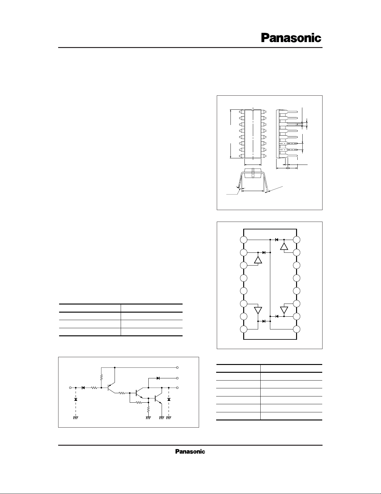
■ Block Diagram
1
Others
DN8690
4-circuit Darlington Driver Array (High Breakdown Voltage : 60V, Large
Drive Current : 1.5A)
1
2
3
4
5
6
7
8
16
15
14
13
12
11
10
9
19.2±0.3
1.22±0.25
3 ∼15˚
Unit : mm
6.2±0.3
0.5±0.1
2.54
5.2±0.25
16-pin DIL Plastic Package (DIP016-P-0300D)
3.05±0.25
7.62±0.25
0.3
+
0.1
– 0.05
1.1±0.25
■ Schematic Circuit (1 Circuit)
1 16
2 15
3 14
4 13
5 12
6 11
7 10
8
Common
Q
1
I
1
GND
GND
I
2
N. C.
Q
2
Q
4
I
4
V
CC
GND
GND
I
3
Q
3
Common
9
■ Function Table
Input (In) Output (Qn)
L
H
OPEN
Q
R
1
1
8kΩ
I
L
H
H
■ Pin Descriptions
V
Q
20kΩ
R
2
Q
2
R
3
1.2kΩ
R
5kΩ
Q
4
5
3
Q
4
1kΩ
R
5
CC
Common
Q
Symbol Pin name
Common
to Q
Q
1
I1 to I
GND
V
CC
NC
4
4
Clamp diode pin
Output pin
Input pin
Ground pin
Power pin
No connection

2
Others
DN8690
V
CC
V
CE (sus)
I
O
V
I
V
R
I
F
P
D
T
opr
T
stg
Supply voltage
Output breakdown
Output current
Input voltage
Clamp diode breakdown
Clamp diode forward current
Power dissipation
Operating ambient temperature
Storage temperature
V
V
A
V
V
A
W
˚C
˚C
7.0
60
1.5
0 to 30
60
1.5
2.0
– 20 to + 75
– 55 to + 150
Parameter Symbol Rating Unit
■ Absolute Maximum Ratings (Ta =25˚C)
Input voltage
V
IH
30 V
V
CC
= 3.5 to 7V
V
IL
V
V
CC
= 3.5 to 7V
V
CE (sat)
1 1.2 V
V
I
= 0V, IO = 0.5A
Output saturation voltage
V
CE (sat)
2V
V
I
= 0V, IO = 1A
V
CE (sat)
3V
V
I
= 0V, IO = 1.5A
mA
V
CC
= 7V, VI = 0V
Input current
I
I
V
I
O
= 100µA
Output breakdown
V
CE (sus)
µA
V
CC
= 7V, Total VI = 7V
Supply current
I
CCH
mAI
CCL
V
V
CC
= 7V, VI = 0V (1 circuit)
Clamp diode forward voltage
V
F
µA
I
F
= 1.5A
30
3.0
50
8.0
1.5
V
CC
– 2.6
2.0
1.0
V
CC
– 0.3
0
60
Clamp diode reverse current
I
R
VR = 60V, VO = 0V
µs0.2
V
M
= 60V, RI = 50Ω
Propagation delay time
t
PHL
µs5.0t
PLH
V
CC
= 5V, CI = 15pF
Parameter Symbol Condition min typ max Unit
■ Electrical Characteristics (VCC= 5V, Ta= 25˚C)
 Loading...