

Panasonic DN8667NS Datasheet
1
Others
■ Overview
The DN8667NS is a semiconductor integrated circuit
which incorporates a 8-bit shift register, a latch driver and
a constant current driver to satisfy the demand for equalization of LED panel brightness. It also incorporates the
serial-in and serial-out/parallel-out functions. It employs
the Bi-CMOS process : The 8-step shift register block
and latch block consist of CMOS while the 8-step parallel
driver block is bipolar.
■ Features
•
Serial-in, serial-out/parallel-out
•
Cascade connection possible
•
Constant current output (0 to 100 mA able to be set by
one external resistor)
•
Output-forced ON/OFF terminal attached (EN)
•
Input/Output CMOS compatible
■ Application
•
LED panel drive
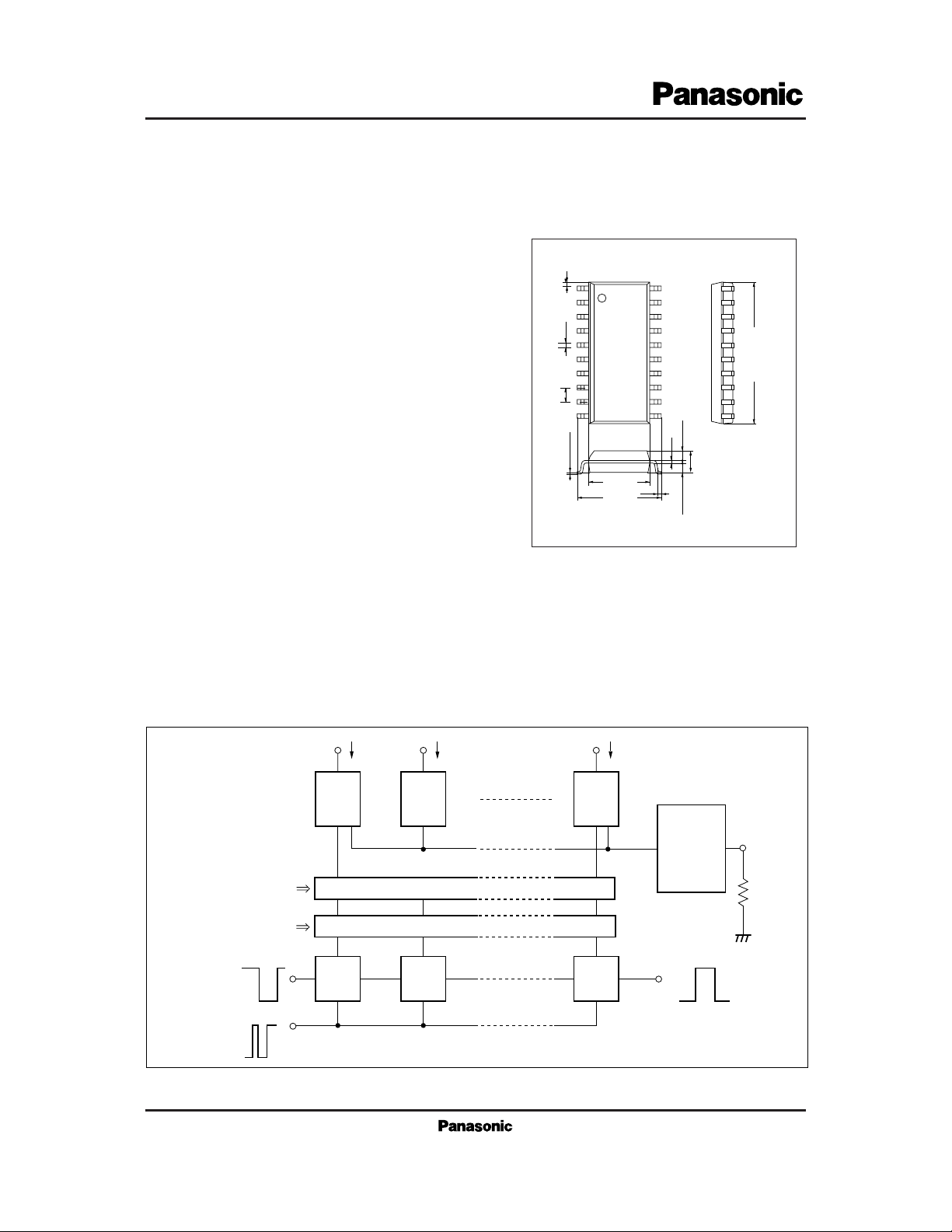
DN8667NS
8-Bit Shift Register Latch Constant Current Driver IC
1
2
3
4
5
6
7
8
9
10
20
19
18
17
16
15
14
13
12
11
5.5±0.3
7.6±0.3
(0.4)
1.27
0.9±0.25
2.05±0.2
0.9±0.25
0.2
– 0.05
+ 0.1
0.4±0.25 (0.4)
12.63±0.3
Unit : mm
0.1±0.1
20-pin SOP Package (SOP020-P-0300A)
■ Block Diagram
Gate Control Sig.
Latch Control Sig.
Data Input
Clock Input
12 8
Constant
Current
Output
Constant
Current
Output
Constant
Current
Output
Gate
Latch
Shift
Register
Shift
Register
Shift
Register
Current Set.
Data Output
Resistor
External
2
OthersDN8667NS
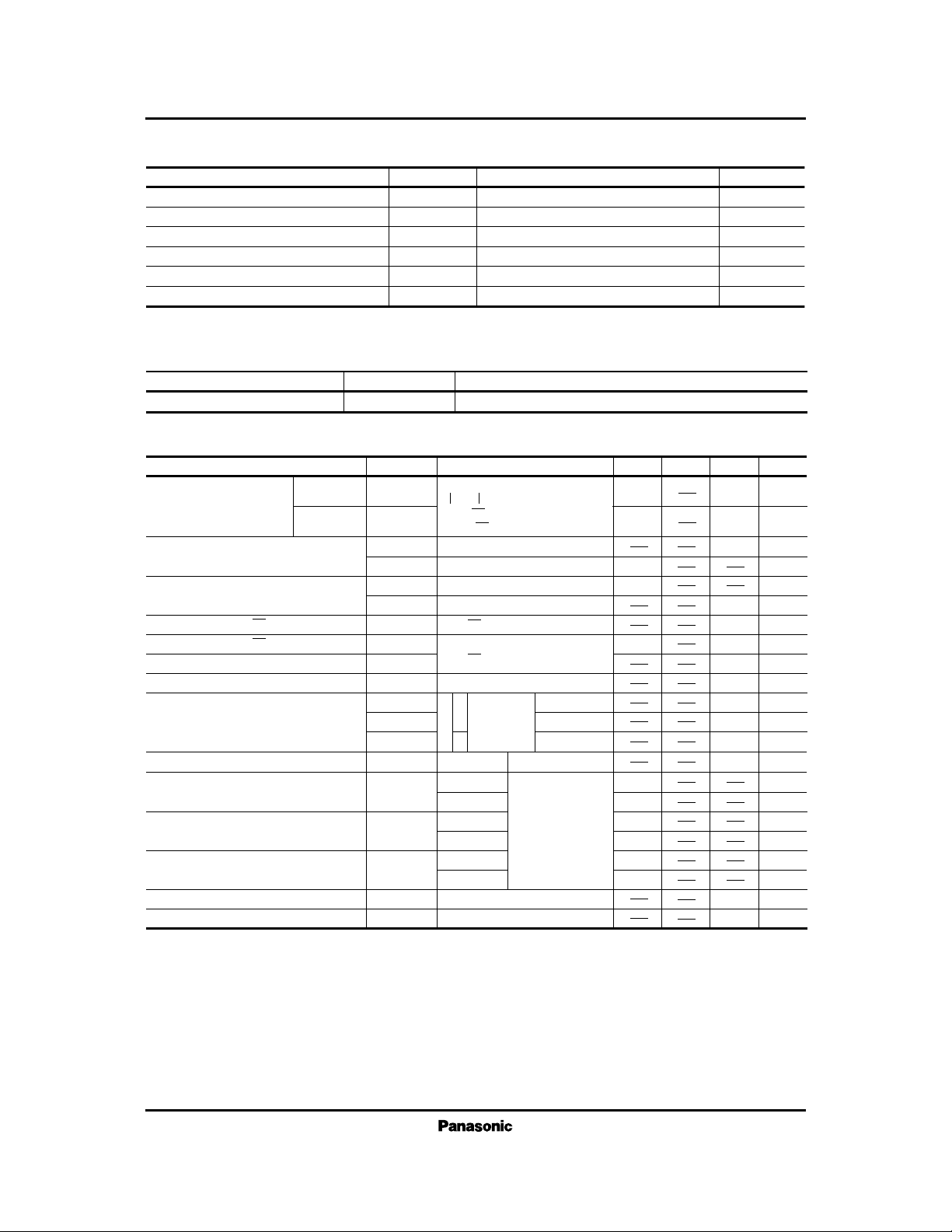
Parameter Symbol Rating Unit
■ Absolute Maximum Rating (Ta = 25˚C)
*
For printed board SM, it decreases with rate of 10.24 mW/˚C from Ta = 25 ˚C.
Supply voltage
Output voltage
Output current
Power dissipation
*
Operating ambient temperature
Storage temperature
V
CC
V
O
I
O
P
D
T
opr
T
stg
0 to + 7.0
0 to + 14
150
1.28
–20 to + 85
–55 to + 150
V
V
mA
W
˚C
˚C
■ Recommended Operation Range (Ta=25 ˚C)
V
CC
Operating supply voltage
Parameter Symbol Range
4.5V to 5.5V
Note) VCC= 5V unless otherwise specified.
CLK
CLK
STB
SIN
STB
SIN
STB
Parameter Symbol Condition min typ max Unit
■ Electrical Characteristics (VCC=5V,Ta=25 ± 2˚C)
Input voltage
Positive direction
Negative direction
0.35V
CC
V
T+
0.7V
CC
V
V
SOUT
= 0.1, V
CC
– 0.1V
I
SOUT
= 20µA
Input current
0.2V
CC
4.0
83
20
20
20
15
20
10
V
T–
0.55V
CC
V
V
1H
= 5.0VI
IH
– 25
25
µA
mA
mA
mA
V
1L
= 0VI
IL
µA
µA
25
VO= 14V (Output OFF)I
OLK
2
mA
20
mA
MH
Z
ns
30
20
Output voltage (SOUT)
Output current 1 (Qn)
Output current 2 (Qn)
Output current error between bits
Output leak current
I
OH
= – 0.4mA
VCC=5.5V
V
OH
0.5
I
OL
= 1.6mAV
OL
I
ref
= 0mAI
CC1
I
ref
= –2.5mA
Input Duty 40 to 60%
I
CC2
I
ref
= –2.5mAI
CC3
f
CLK
t
w
t
su
t
h
t
r
t
f
100
117
V
O
(Qn) = 0.5V
I
OI
I
OI
±6
V
CC
= 5.0V, I
ref
= –12mA
V
O
(Qn) = 1.0V
DI
O
V
V
%
{
I
O
(Qn) = –10µA, 90mA
V
O
(Qn) =
0.6V I
ref
= –
2.5mA
{
Total Driver Output
OFF ON
Supply current
Input pulse width
Clock frequency
Setting-up time
Holding time
Clock pulse rise time
Clock pulse fall time
500
500
ns
ns
ns
ns
ns
ns
ns
V
CC
=5.0V
R
L
=50Ω
C
L
=15pF
 Loading...