

Panasonic DN8648FBP Datasheet
1
Others
■ Overview
The DN8648FBP is an IC which incorporates a 32-bit shift
register and a latch driver to meet high-speed operation low
power consumption and high-density printout of the thermal
printers for the work processors, and so on. It employs the BiCMOS process in which the serial-in and serial-out/parallel-out
functions are incorporated, the 32-step shift register block and
latch block are composed of CMOS, and the 32-step parallel
driver block is bipolar.
■ Features
• Serial-in and serial-out/parallel-out
• Cascade connection allowed
• Built-in output malfunctioning preventive circuit
• Low current consumption at standby I
CC
≤ 100µA
• High-breakdown, large current drive type output steps
Breakdown voltage : 30V
Output current : 120mA (per pin)
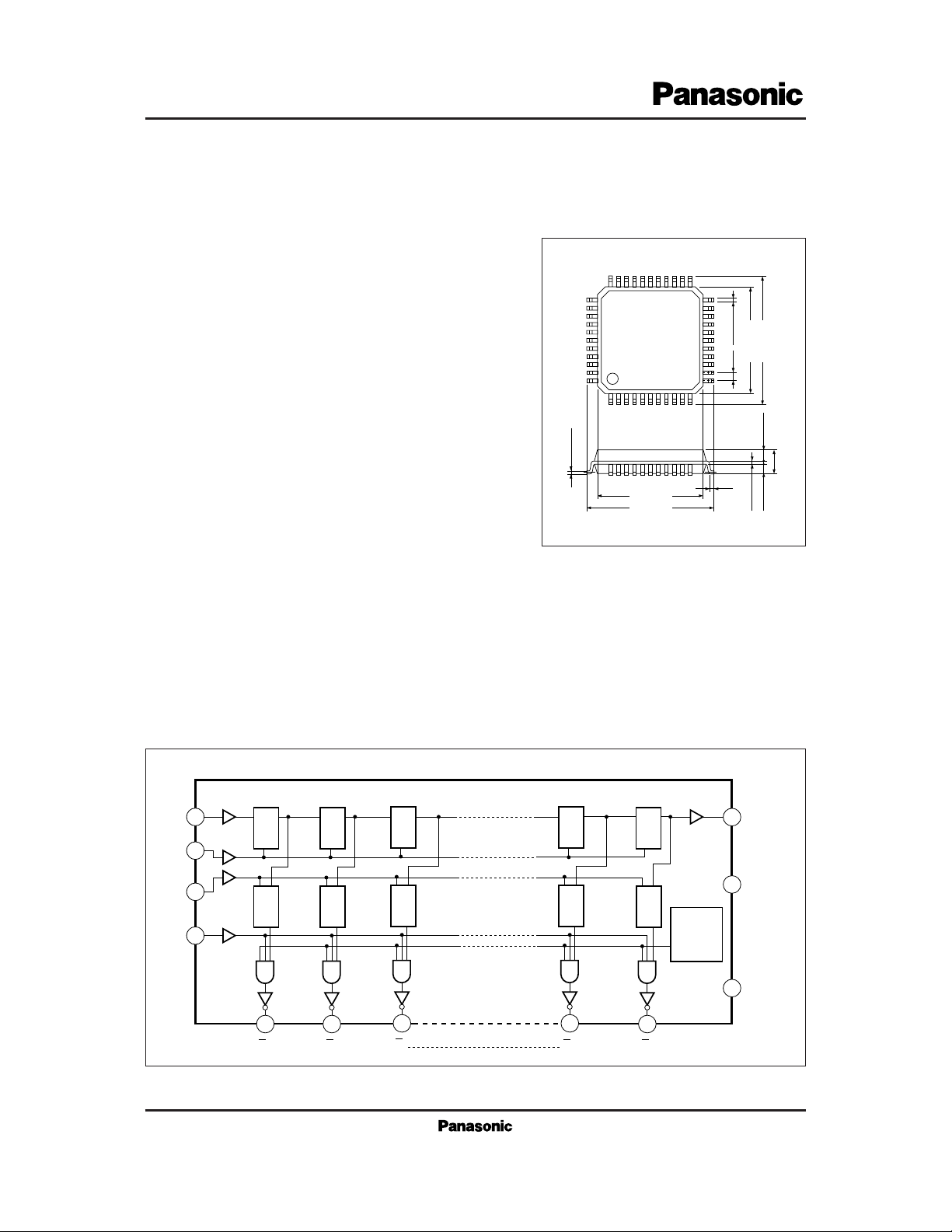
• Surface mountable 44-pin flat package (pin pitch : 0.8mm)
■ Applications
• Driving of the thermal heads
• Driving of the relays, LEDs, solenoids, etc.
DN8648FBP
32-bit Shift Register Latch Driver IC
111
33 23
12
22
34
44
0.35±0.10.8
Unit : mm
10.0±0.3
2.85±0.2
1.3±0.11.3±0.1
0.2
0.6
+ 0.1
– 0.05
12.2±0.3
0.1±0.1
10.0±0.3
12.2±0.3
44-pin QUADFLAT Package (QFH044-P-1010 )
■ Block Diagram
SIN
CLK
STB
EN
38
35
36
37
DCPQ
LQD
DCPQ
LQD
DCPQ
LD
Q
DCPQ
LD
Q
DCPQ
LD
Q
Output
malfunction
protector
39
34
SOUT
V
CC
GND
6, 7, 27, 28
31
Q
3
33 32
Q
1
Q
2
43
Q
31
42
Q
32
2
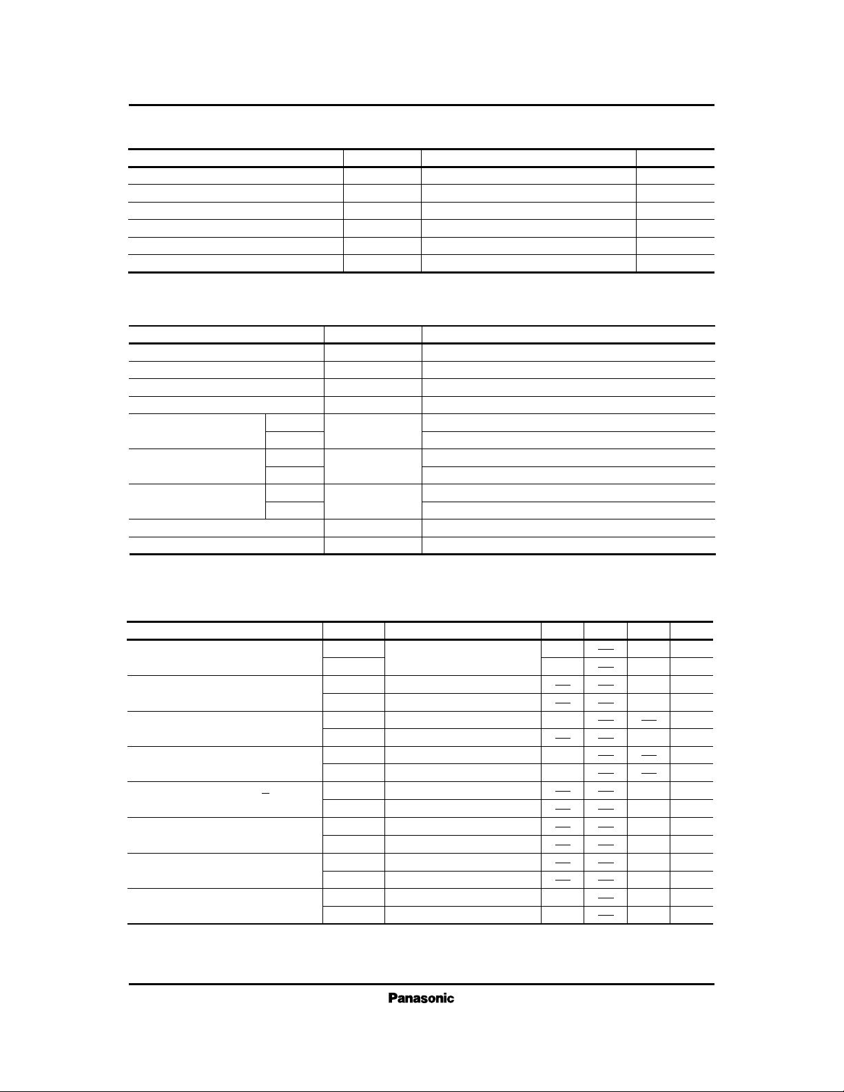
Others
DN8648FBP
V
CC
V
O
I
O
P
D
T
opr
T
stg
Supply voltage
Output voltage
Output current
Power dissipation
Operating ambient temperature
Storage temperature
V
V
mA
W
˚C
˚C
0 to 7
0 to 30
120 (Per one circuit)
1.8
*
– 20 to + 75
– 55 to + 125
*
When mounting onto the PCB, power dissipation is reduced at a rate of 15mW/˚C from Ta= 25˚C.
Parameter Symbol Rating Unit
■ Absolute Maximum Ratings (Ta = 25˚C)
Operating supply voltage
Output voltage
Output current
Clock frequency
Input pulse width
Setup time
Hold time
CLK
STB
over 40ns
over 40ns
SIN
STB
SIN
STB
over 30ns
over 40ns
over 20ns
over 0ns
Clock pulse rise time
Clock pulse fall time
*
1
An allowable value changes depends on the number of simultaneously turned-on circuits and the duty. Use with power dissipation taken into full account.
*
2 Input duty : 40 to 60%
V
CC
V
O
I
O
f
CLK
t
w
t
su
t
h
t
r
t
f
4 to 6V
below 30V
below 100mA
*
1
below 10MHz
*
2
below 500ns
below 500ns
Parameter Symbol Range
■ Recommended Operating Range (Ta=25˚C)
Input voltage
0.7V
CC
V
IH
V
CC
V
VCC= 4 to 6V
0V
IL
0.3V
CC
V
Input current
I
IH
25 µA
V
IH
= 5V
I
IL
– 25 µA
V
IL
= 0V
I
OL
=100mA
IOL= 80mA
VO= 30V (output OFF)
Output saturation voltage (Qn)
V
CE (sat) 1
0.4 V
V
CE (sat) 2
0.35 V
Output leakage current
I
OLK1
50 µA
*
VCC=5V unless otherwise specified
I
OLK2
µA
V
O
=15V (output OFF)
Supply current
I
CC1
100 µA
Total driver output OFF
25
I
CC2
5mA
Driver output 1 circuit ON
Output voltage (SOUT)
V
OH
V
I
O
= –1µA
V
OL
0.1 V
I
O
=1µA
4.9
Output current (SOUT)
I
OH
mA
V
OH
= 4.5V
I
OL
mA
V
OL
= 0.4V
– 4
4
Output malfunctioning preventive
Circuit operating voltage
2.9V
CCT
+
3.9 V
*
2.6V
CCT
–
3.6 V
*
Parameter Symbol Condition min typ max Unit
■ Electrical Characteristics (Ta=25˚C)
 Loading...