

Panasonic DN8643S Datasheet
■ Overview
The DN8643S is an IC which incorporates a 24-bit shift register and a latch driver to meet high-speed operation, low
power consumption and high-density printout of the thermal
printers for the work processors, and so on. It employs the BiCMOS process in which the serial-in and serial-out/parallel-out
functions are incorporated, the 24-step shift register block and
latch block are composed of CMOS, and the 24-step parallel
driver block is bipolar.
■ Features
•
Serial-in and serial-out/parallel-out
•
Cascade connection allowed
•
Built-in output malfunctioning preventive circuit
•
Low current at stanby ICC=≤100µA
•
High-breakdown, large current drive type output steps
Breakdown : 30V
Output current : 120mA
•
Surface mountable USONF-36D package (pin pitch :
0.8mm)
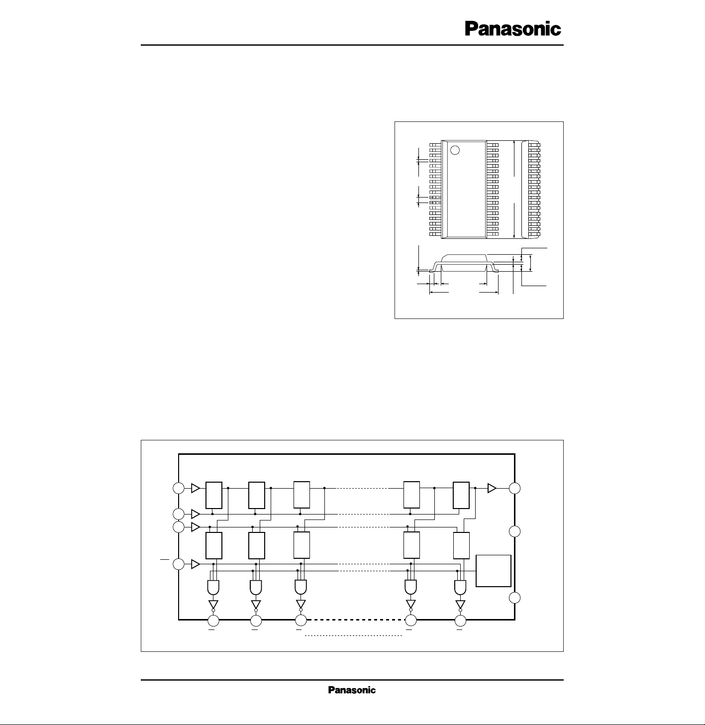
DN8643S
24-bit Shift Register Latch Driver IC
15.2±0.3
11.93±0.3
8.4±0.3
0.5
2.85±0.2
0.2
+0.1
– 0.05
1.3±0.25
1.3±0.25
0.35±0.25
0.8
36-pin PANAFLAT Plastic Package (SSOP036-P-0450)
Unit : mm
0.1±0.1
1
18
36
19
■ Block Diagram
SIN
CLK
STB
EN
17
18
19
1
DCPQ
LQD
DCPQ
LQD
DCPQ
LD
Q
DCPQ
LD
Q
DCPQ
LD
Q
Output
Malfunction
Protector
20
SOUT
36
V
CC
GND
8, 9, 10
27, 28, 29
16 15
Q
1
14
Q
2
Q
3
22
Q
23
21
Q
24
V
CC
V
O
I
O
P
D
T
opr
T
stg
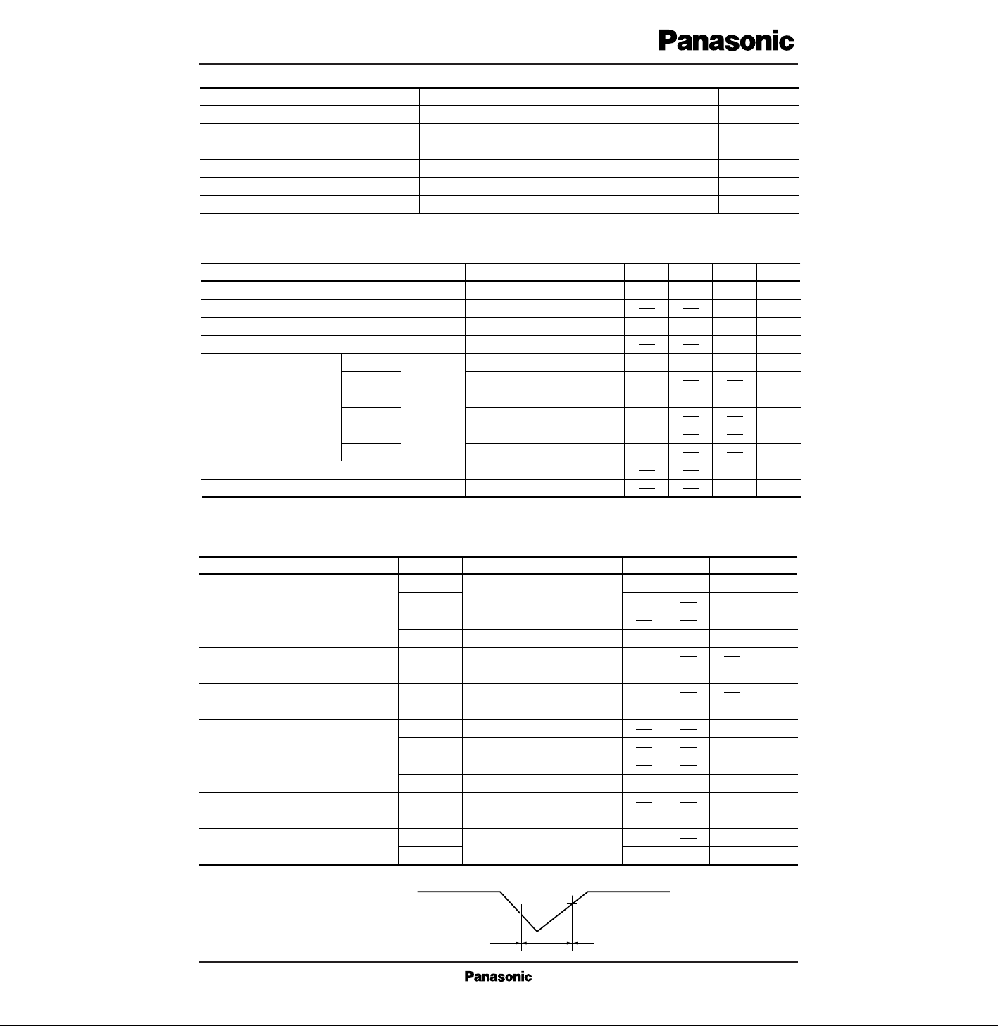
Supply voltage
Output voltage
Output current
Power dissipation
Operating ambient temperature
Storage temperature
V
V
mA
W
˚C
˚C
0 to 7
0 to 30
120
1.3
*
–20 to + 75
–55 to + 125
*
When mounting onto the PCB, power dissipation is reduced at a rate of 10.4mW/˚C from Ta=25˚C
Parameter Symbol Rating Unit
■ Absolute Maximum Ratings (Ta=25˚C)
Parameter Symbol Condition mim typ max
■ Recommended Operating Range (Ta=25˚C)
Supply voltage
V
CC
6 V5
Output voltage
V
O
V
Output current
*
I
O
100 mA
30
4
Clock frequency
f
CLK
10 MHz
Input Duty 40 to 60%
Input pulse width
t
w
ns40
ns40
Setup time
t
su
ns30
ns40
Hold time
t
h
ns20
CLK
STB
SIN
STB
SIN
STB ns0
Clock pulse rise time
t
r
500 ns
Clock pulse fall time
t
f
500 ns
Unit
*
An allowable value changes depends on the number of simultaneously turned-on circuits and the duty. Use with power dissipation
taken into full account.
Input voltage
0.7V
CC
V
IH
V
CC
V
VCC=4 to 6V
0V
IL
0.3V
CC
V
Input current
I
IH
25 µA
V
IH
=5V
I
IL
–25 µA
V
IL
=0V
I
OL
=100mA
IOL=80mA
VO=30V (output OFF)
Output saturation voltage
V
CE (sat) 1
0.4 V
V
CE (sat) 2
0.35 V
Output leakage current
I
OLK1
50 µA
*
Output malfunctioning preventive circuit operating voltage timing chart
I
OLK2
µA
V
O
=15V (output Off)
Supply current
I
CC1
100 µA
Total driver output OFF
25
I
CC2
5 mA
Driver output 1 circuit ON
Output voltage
V
OH
V
I
O
= –1µA
V
OL
0.1 V
I
O
=1µA
4.9
Output current
I
OH
mA
V
OH
=4.5V
I
OL
mA
V
OL
=0.4V
–4
4
Output malfunctioning preventive
circuit operating voltage
*
2.9V
CCT
+
3.9 V
2.6V
CCT
–
3.6 V
OFF
Driver output
V
CCT
+
V
CCT
–
V
CC
Enable Enable
Parameter Symbol Condition min typ max Unit
■ Electrical Characteristics (Ta=25˚C)
 Loading...