


Panasonic CQRDP-102-N, CQRDP-112-N, CQRDP-142-N, CQRDP-152-N, CQRDP-162-N Service manual
ORDER No. ACED020483C8
AUTOMOTIVE CONSUMER ELECTRONICS
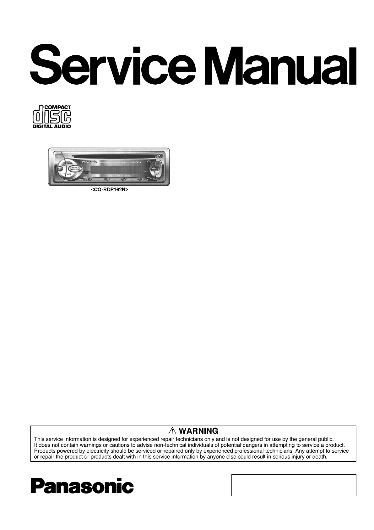
CQ-RDP162N
CQ-RDP112N
CQ-RDP152N
CQ-RDP142N
CQ-RDP102N
CD Player / Receiver with CD Changer
Control
Specification*
General
Power Supply DC 12V (11V - 16V),
Test Voltage 14.4V
Negative Ground
Tone Controls Bass ; ±12dB at 100Hz
Treble ; ±12dB at 10kHz
Current Consumption Less than 2.5A (CD play mode,
0.5W×4ch)
Maximum Power Output 45W×4ch (at 4Ω)
Power Output 20W×4 (DIN45 324, at 4Ω)
Speaker Impedance 4-8Ω
Pre-Amp Output Voltage 2V (CD mode)
Pre-Amp Output Impedance 600Ω
FM Stereo Radio
Frequency Range 87.5 - 108MHz
Usable Sensitivity 6dB/µV (S/N 30dB)
LW Radio
Frequency Range 153 - 279kHz
Usable Sensitivity 32dB/µV (S/N 20dB)
MW Radio
Frequency Range 531 - 1,602kHz
Usable Sensitivity 28dB/µV (S/N 20dB)
CD Player
Sampling Frequency 8 times oversampling
Pick-Up Type Astigma 3-beam
Light Source Semiconductor Laser
Wavelength 780nm
Frequency Response 20Hz to 20,000Hz (±1dB)
Signal to Noise Ratio 96dB
Dimensions** 178×50×150mm
Weight** 1.4kg
* Specifications and the design are subject to possible modification
without notice due to improvements.
** Dimensions and Weight shown are approximate.
© 2002 Matsushita Communication Industrial Co.,
Ltd. All rights reserved. Unauthorized copying and
distribution is a violation of law.
CQ-RDP162N / CQ-RDP112N / CQ-RDP152N / CQ-RDP142N / CQ-RDP102N
CONTENTS
Page Page
1 FEATUERS 2
2 LASER PRODUCTS
3 REPLACEING THE FUSE
4 MAINTENANCE
5 NOTES
6 DIMENSIONS
7 WIRING CONNECTION
8 BLOCK DIAGRAM
9 TERMINALS DESCRIPTION
10 PACKAGE AND IC BLOCK DIAGRAM 7
2
11 REPLACEM ENT PARTS LIST
2
12 EXPLODED VIEW (Unit)
13 CD PLAYER MECHANICAL PARTS LIST
2
2
14 EXPLODED VIEW (CD Deck)
2
15 WIRING DIAGRAM
16 SCHEMAT IC DIAGRAM -1
3
4
17 SCHEMAT IC DIAGRAM -2
5
10
15
16
17
18
22
23
1 FEATUERS
∙
PLL (Phase Locked Loop) synthesized tuning.
∙
18-FM, 6-AM presets with preset scan
∙
RDS (Radio Data System) reception.
∙
Digital servo for reliable CD playback.
∙
Removable face plate.
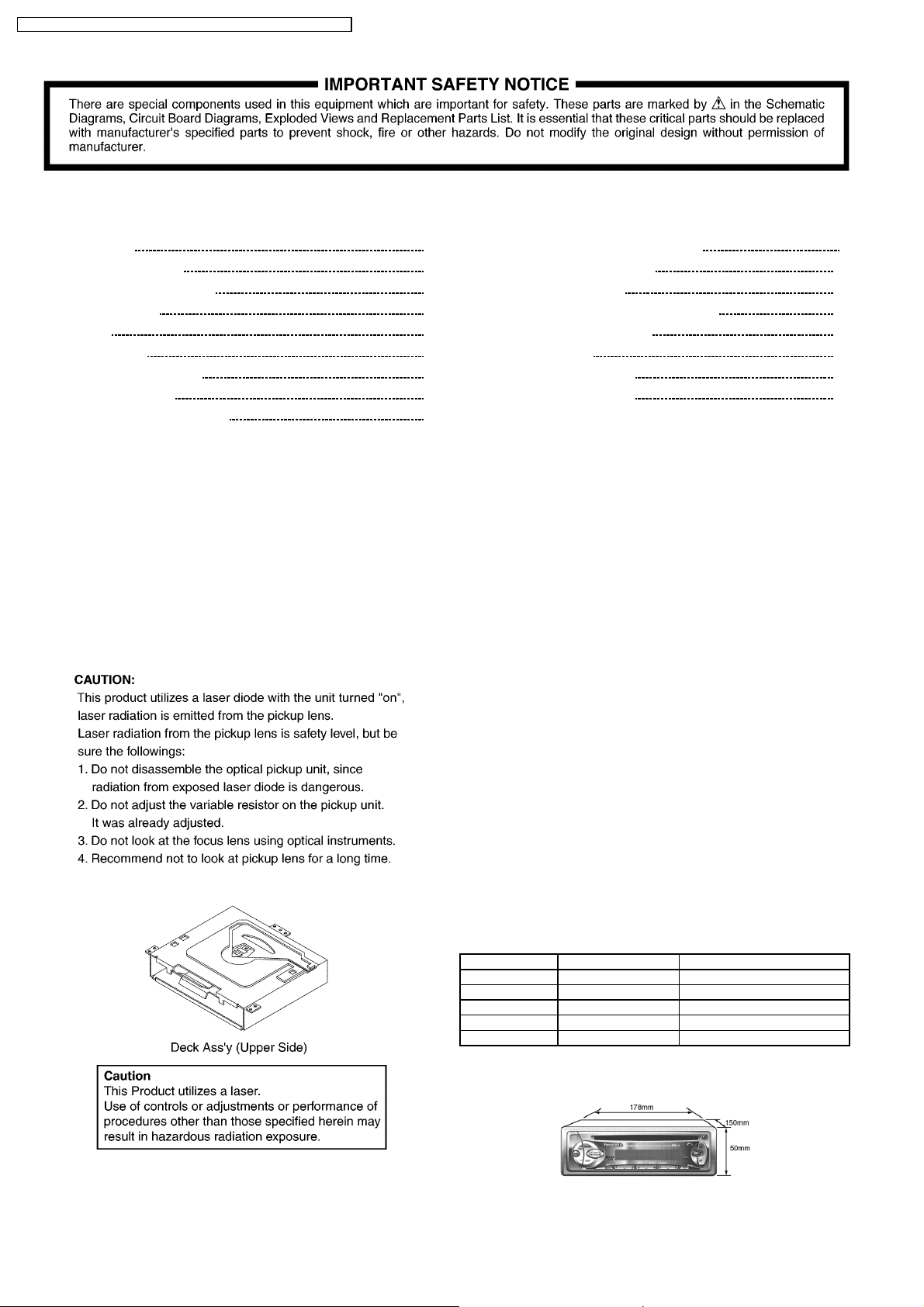
2 LASER PRODUCTS
3 REPLACEING THE FUSE
Use fuses of the same specified rating (15A). Using different
substitutes or fuses with higher ratings, or connecting the
product directly without a fuse, could cause fire or damage to
the stereo unit.
4 MAINTENANCE
Your products is designed and manufactured to ensure a
minimum of maintenance. Use a dry, a soft cloth for routine
exterior cleaning. Never use benzine, thinner or other solvents.
5 NOTES
[RADIO BLOCK]
Do not align the AM/FM package block. When the package
block is necessary, it will be supplied already aligned at the
factory.
[CD DECK BLOCK]
This model has no servo alignment points because
microcomputer controls the servo circuit.
[OTHER]
This operating instruction manual applies to the five models
below. All illustrations represent model CQ-RDP162N unless
otherwise specified.
Changer Control Illumination Color
CQ-RDP162N Yes Amber
CQ-RDP112N Yes Green
CQ-RDP152N None Amber
CQ-RDP142N None Red
CQ-RDP102N None Green
6 DIMENSIONS
2
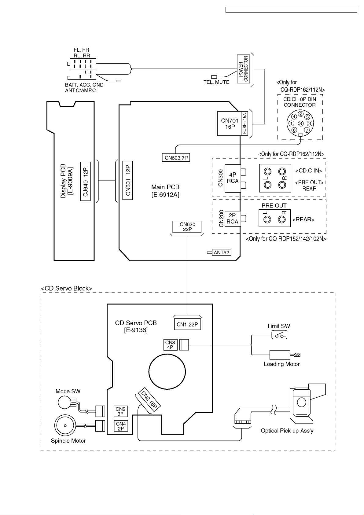
7 WIRING CONNECTION
CQ-RDP162N / CQ-RDP112N / CQ-RDP152N / CQ-RDP142N / CQ-RDP102N
3
CQ-RDP162N / CQ-RDP112N / CQ-RDP152N / CQ-RDP142N / CQ-RDP102N
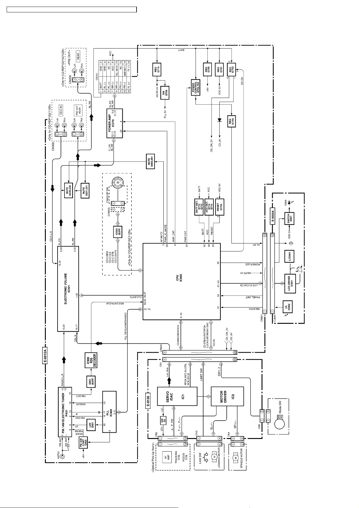
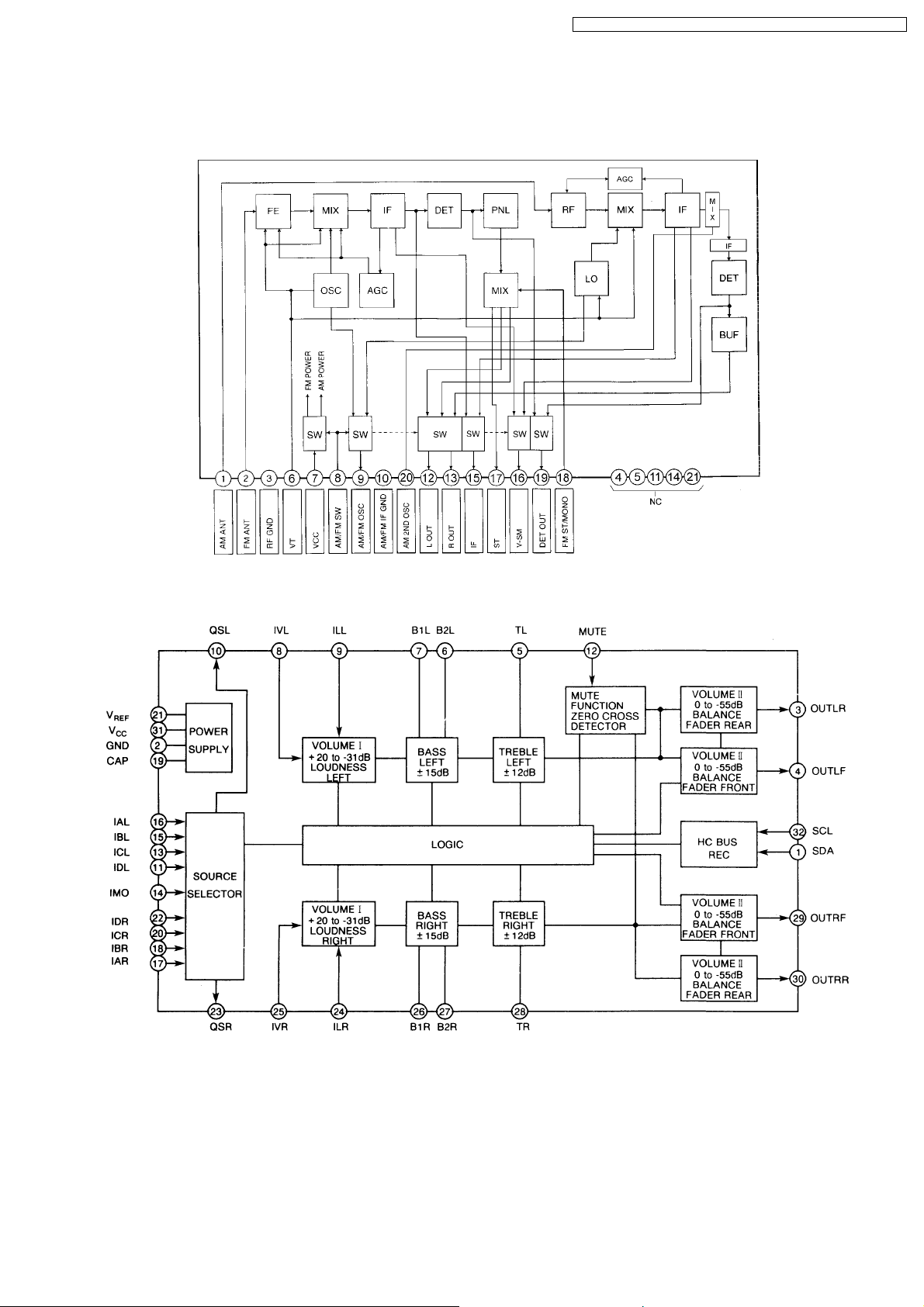
8 BLOCK DIAGRAM
4
9 TERMINALS DESCRIPTION
CQ-RDP162N / CQ-RDP112N / CQ-RDP152N / CQ-RDP142N / CQ-RDP102N
9.1. Main Block
IC600 : C2CBHF000217
Pin
No.
Port Descriptions I/O
1 NC (Connecting to ground) - 0 0 0
2 NC (Connecting to ground) - 0 0 0
3 NC (Connecting to ground) - 0 0 0
4 AVSS Analog ground - 0 0 0
5 AF MUTE AF mute O 5.1 5.1 5.2
6 AMP-CNT Power Amp. stand-by O 5.1 5.1 5.2
7 AVREF Reference voltage - 5.1 5.1 5.2
8 CD-MISO CD data I 0 0 0
9 CD-MOSI CD data O 0 0 2.4
10 CD-SCK CD clock O 0 0 5.1
11 CD.C DATA CD.CH data I 0 0 0
12 NC No connection - - - 13 CD.C CLK CD.CH data shift clock I 0 0 0
14 REM OUT CD.CH remote cont. O 5.0 5.0 5.0
15 BZOUT Beep output O 0 0 0
16 PLL-MISO Data from PLL I 5.1 5.1 5.1
17 PLL-MOSI Data for PLL O 0 0 0
18 PLL-CLK Clock for PLL O 5.1 5.1 5.2
19 PLL-CE PLL chip enable O 0 0 0
20 NC No connection - - - 21 NC No connection - - - 22 NC No connection - - - 23 NC No connection - - - 24 CD-STB CD strobe O 0 0 5.1
25 CD-A0 CD address 0 O 0 0 4.4
26 CD-RST CD reset O 0 0 5.1
27 CD-RFOK CD RFOK signal I 0 0 5.0
28 CD-LOCK CD lock signal I 0 0 5.0
29 CD-LIMIT CD limit sw I 0 0 5.1
30 CD-SW2 CD SW2 I 5.1 5.1 0
31 NC No connection - - - 32 NC No connection - - - 33 Vss Ground - 0 0 0
34 S.LED Not used - - - 35 ST-IND FM stereo detection I 5.0 5.1 5.1
36 IC2-CLK Electronic volume clock O 5.1 5.1 5.2
37 IC2-DATA Electronic volume data I/O 5.1 0 5.2
38 NC No connection - - - 39 NC No connection - - - 40 NC No connection - - - 41 LCD-MOSI LCD data output O 0 0 0
42 LCD-MISO LCD data input I 5.0 5.0 5.0
43 LCD-CLK LCD clock O 0 0 0
44 LCD-CE LCD chip enable o utput O 0 0 0
45 POWER LED Pilot lamp on O 0 0 0
46 ANT.CONT Motor antenna control O 5.1 5.1 0
47 NC No connection - - - 48 NC No connection - - - 49 REM-IN_SUB Remote control sig.
50 NC No connection - - - 51 NC No connection - - - 52 NC No connection - - - 53 NC No connection - - - 54 TEL-MUTE Not used - - - 55 PANEL-DET Panel detect I 0 4.8 4.9
56 CD-ON CD power control O 0 0 5.1
57 PWR CNT Power control O 5.0 5.0 5.0
58 ACC-DET ACC detection I 5.1 5.1 5.1
59 RDS DATA RDS data I 2.5 0 0
60 /RESET Reset input I 5.1 5.1 5.1
61 REM Remocon data input I 4.4 4.4 4.4
62 BATT Battery detection I 5.1 5.1 5.1
63 RDS CLK RDS clock I 2.5 0 0
64 CD.C.STB CD.CH data strobe I 0 0 0
65 PWR-IC-MUTE Mute control O 5.1 5.1 5.1
66 CD-INSW1 CD insert detection SW I 0 0 0
sampling
(V)FM(V)AM(V)CD(V)
I 0 4.4 4.4
Pin
No.
67 VSS Ground - 0 0 0
68 VDD +5V power supply - 5.1 5.1 5.1
69 X2 Crystal oscillator - 3.1 3.1 3.1
70 X1 Crystal oscillator - 2.2 2.2 2.2
71 Vpp (Ground pull-down) - 0 0 0
72 SUB-X2 Crystal oscillator - 3.1 3.1 3.1
73 SUB-X1 Crystal oscillator - 2.5 2.5 2.5
74 AVDD +5V power supply - 5.1 5.1 5.1
75 AVREF (Connecting to VDD) - 5.1 5.1 5.1
76 VSM_DET S-meter detection I 0 0 0
77 INIT A Initial value A I 5.1 5.1 5.1
78 INIT B Initial value B I 5.1 5.1 5.1
79 INIT C Initial value C (Note2)I (#1) (#1) (#1)
80 INIT D Initial value D I 0 0 0
Port Descriptions I/O
(V)FM(V)AM(V)CD(V)
Note 1 :
Voltage measuerments are with respect to ground, with a
voltmeter (internal resistance : 10M ohms).
Note 2 : (#1)
5.5V <CQ-RDP162/112N>
0V <CQ-RDP152/142/102N>
9.2. Display Block
IC901 : YEAMLC75854T
Pin No. Port Descriptions I/O
1-8 SEG1-8 LCD segment O 2.5
9-35 SEG9-35 LCD segment O 2.5
36-39 NC No connection - 40-43 COM1-4 LCD common O 2.5
44-49 KS1-6 Key data output O 0.9
50-54 KI1-5 Key data input I 0
55 TEST (Connecting to ground) - 0
56 VDD +5V power supply - 5.1
57 VDD1 Ground through capacitor - 3.3
58 VDD2 Ground through capacitor - 1.7
59 Vss Ground - 0
60 OSC CR oscillator - 3.9
61 DO Key data output O 4.4
62 CE Chip enable I 0
63 CLK LCD clock I 0
64 DI LCD data input I 0
(V)
(V)
5
CQ-RDP162N / CQ-RDP112N / CQ-RDP152N / CQ-RDP142N / CQ-RDP102N
9.3. CD Servo Block
IC1 : C1BB00000665
Pin
No.
Port Descriptions I/O Vol.
1 D.GND Digital logic Ground - 0
2 RFOK RFOK output signal O 5.0
3 /RST System reset I 5.1
4 A0 Command/Parameter specification I 4.5
5 /STB Serial data strobe I 5.1
6 /SCK Data shift clock I 5.1
7 SO Serial data O 0
8 SI Serial data I 2.4
9 XTALEN (Connecting to ground) - 0
10 D.VDD Digital logic power supply - 5.0
11 DA.VDD DAC power supply - 4.8
12 R_OUT Audio R ch O 2.4
13 DA.GND DAC ground - 0
14 REGC Bypass capacitor for SCF
15 DA.GND DAC ground - 0
16 L_OUT Audio L ch O 2.4
17 DA.VDD DAC power supply - 4.8
18 R+ Not used - 19 R- Not used - 20 L- Not used - 21 L+ Not used - 22 X.VDD Crystal OSC power supply - 5.0
23 /XTAL Crystal OSC terminal - 2.4
24 XTAL Crystal OSC terminal - 2.2
25 X.GND Crystal OSC ground - 0
26 D.VDD Digital logic power supply - 5.0
27 EMPH Not used - 28 FLAG Not used - 29 DIN DAC serial data I 2.6
30 DOUT DAC serial data O 2.6
31 SCKIN DAC shift clock I 2.7
32 SCKO DAC shift clock O 2.7
33 LRCKIN DAC LRCK signal I 2.5
34 LRCK DAC LRCK signal O 2.5
35 HOLD/WDCK Not used - 36 TX Not used - 37 D.GND Digital logic Ground - 0
38 C16M Not used - 39 LIMIT (Connecting to VDD) - 5.0
40 D.VDD Digital logic power supply - 5.0
41 LOCK EFM SYNC detection O 5.0
42 RFCK Not used - 43 MIRR/WFCK Not used - 44 PLCK Not used - 45 D.GND Digital logic Ground - 0
46 C1D1 Not used - 47 C1D2 Not used - 48 C2D1 Not used - 49 C2D2 Not used - 50 C2D3 Not used - 51 D.VDD Digital logic power supply - 5.0
52 PACK Not used - 53 TSO Not used - 54 TSI (Connecting to ground) - 0
55 /TSCK (Connecting to ground) - 0
56 TSTB (Connecting to ground) - 0
57 D.GND Digital logic Ground - 0
58 TEST0 (Connecting to ground) - 0
59 TEST1 (Connecting to ground) - 0
60 ATEST Not used - 2.1
61 A.GND Analog logic Ground - 0
62 FD Focus drive O 2.6
63 TD Traking drive O 2.5
64 SD Sled drive O 2.5
65 MD Spindle drive O 2.6
66 DAC0 Not used - 67 DAC1 Not used - -
regurator
- 2.5
(V)
Pin
No.
100 A.VDD Analog logic power supply - 5.0
Port Descriptions I/O Vol.
68 DAC2 Not used - 69 DAC3 Not used - 70 A.VDD Analog logic power supply - 5.0
71 EFM EFM signal O 2.7
72 ASY Reference voltage for EFM comp. I 2.5
73 C3T Capacitor terminal for 3T
74 RFI RF for EFM data generation I 2.5
75 AGCO RF signal output (after gain
76 AGCI RF-AGC amp input I 2.5
77 RFO RF summing amp output O 2.8
78 EQ2 C/R terminal for RF amp equalizer - 2.6
79 EQ1 C/R terminal for RF amp equalizer - 0.5
80 RF- RF summing amp inverted input I 2.4
81 A.GND Analog logic Ground - 0
82 A Photo detector A input I 2.7
83 C Photo detector C input I 2.5
84 B Photo detector B input I 2.7
85 D Photo detector D input I 2.5
86 F Photo detector F input I 3.0
87 E Photo detector E input I 3.0
88 A.VDD Analog logic power supply - 5.0
89 REFOUT Reference voltage output O 2.5
90 FE- Focus error amp input I 2.5
91 FE0 Focus error amp output O 2.5
92 TE- Tracking error amp input I 2.5
93 TE0 Tracking error amp output O 2.5
94 TE2 Tracking error amp output O 2.6
95 TEC Tracking comparator input I 2.5
96 A.GND Analog logic Ground - 0
97 PD PD detection I 0
98 LD LD control O 3.6
99 PN (Connecting to ground) - 0
detection
adjustment)
(V)
- 2.7
O 2.5
6
CQ-RDP162N / CQ-RDP112N / CQ-RDP152N / CQ-RDP142N / CQ-RDP102N
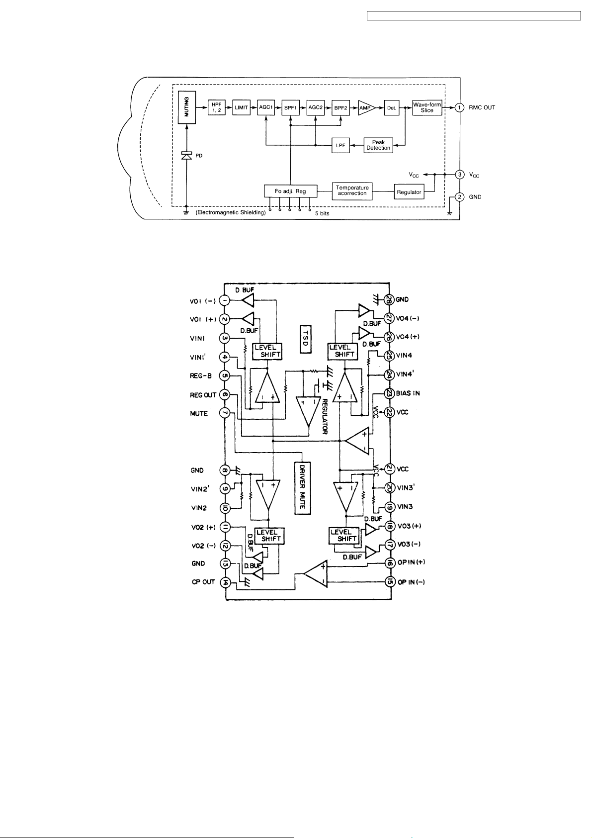
10 PACKAGE AND IC BLOCK DIAGRAM
10.1. Main Block
PA51 : C5BA00000103
IC201 : YEAMEA6320TT
7
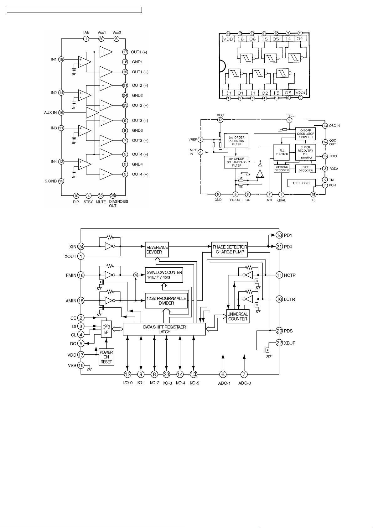
CQ-RDP162N / CQ-RDP112N / CQ-RDP152N / CQ-RDP142N / CQ-RDP102N
IC650 : C0JBAZ000904
IC270 : C1EA00000026
IC900 : YEAMDA7479D
IC400 : C1BB00000541
8
10.2. Display Block
10.3. CD Servo Block
CQ-RDP162N / CQ-RDP112N / CQ-RDP152N / CQ-RDP142N / CQ-RDP102N
IC902 : YEAMSBX8035F
IC2 : C0GBY0000020
9