

Panasonic CQ-DT6930ZE Service Manual
ORDER NO. 3001
AUTOMOTIVE ELECTRONICS
HINO
CQ-DT6930ZE
AM/FM MPX Electronic Tuning Radio
with Cassette Player
HINO PART No. : 86120-37160
VEHICLE : DUTRO
ID CODE : 57270
DESTINATION : ----PRODUCED AFTER : Oct., 2000
Specification
General
Power Supply DC 24V (21.6V - 32V),
Test Voltage 26.4V
Negative Ground
Current Consumption Less than 3.0A
Power Output 15W×4ch
AM Radio
Frequency Range 530 - 1,602kHz
Usable Sensitivity 25dB(µV) (S/N 20dB)
FM Stereo Radio
Frequency Range 88.0 - 108.0MHz
Usable Sensitivity 6dB/µV (S/N 30dB)
Cassette Player
Reproduction System 4-Track, 2-Program Stereo
Tape Speed 4.76cm/sec.
Wow and Flutter Less than 0.1% (WRMS)
Signal to Noise Ratio 53dB (IHF-A)
Dimensions** 178×50×165mm
Weight** 1.3kg
* Specifications and the design are subject to possible modification
without notice due to improvements.
** Dimensions and Weight shown are approximate.
Doldy noise reduction manufactured under license from Dolby
Laboratories Licensing Corporation.
“Dolby” and the double-D symbol
Laboratories Licensing Corporation.
are trade marks of Dolby
© 2001 Matsushita Communication Industrial Co.,
Ltd. All rights reserved. Unauthorized copying and
distribution is a violation of law.
CQ-DT6930ZE
CONTENTS
Page Page
1 FEATUERS 2
2 REAR VIEW AND CONNECTORS
3 FRONT VIEW AND FUNCTIONS
4 WIRING CONNECTION
5 BLOCK DIAGRAM
6 TERMINALS DESCRIPTION
7 PACKAGE AND IC BLOCK DIAGRAM
8 ALIGNMENT INSTRUCTIONS
9 ALIGNMENT POINTS 9
2
10 REPLACEM ENT PARTS LIST
11 EXPLODED VIEW (Unit)
3
3
12 TAPE PLAYER PARTS
4
13 EXPLODED VIEW (Tape Deck)
14 WIRING DIAGRAM
5
6
15 SCHEMAT IC DIAGRAM (1)
9
16 SCHEMAT IC DIAGRAM (2)
1 FEATUERS
10
14
15
17
18
22
23
∙
PLL (Phase Locked Loop) synthesized tuning.
∙
18-station preset (6-AM, 12-FM).
∙
Electronic volume control.
∙
Full logic control tape deck.
∙
Dolby B NR function.
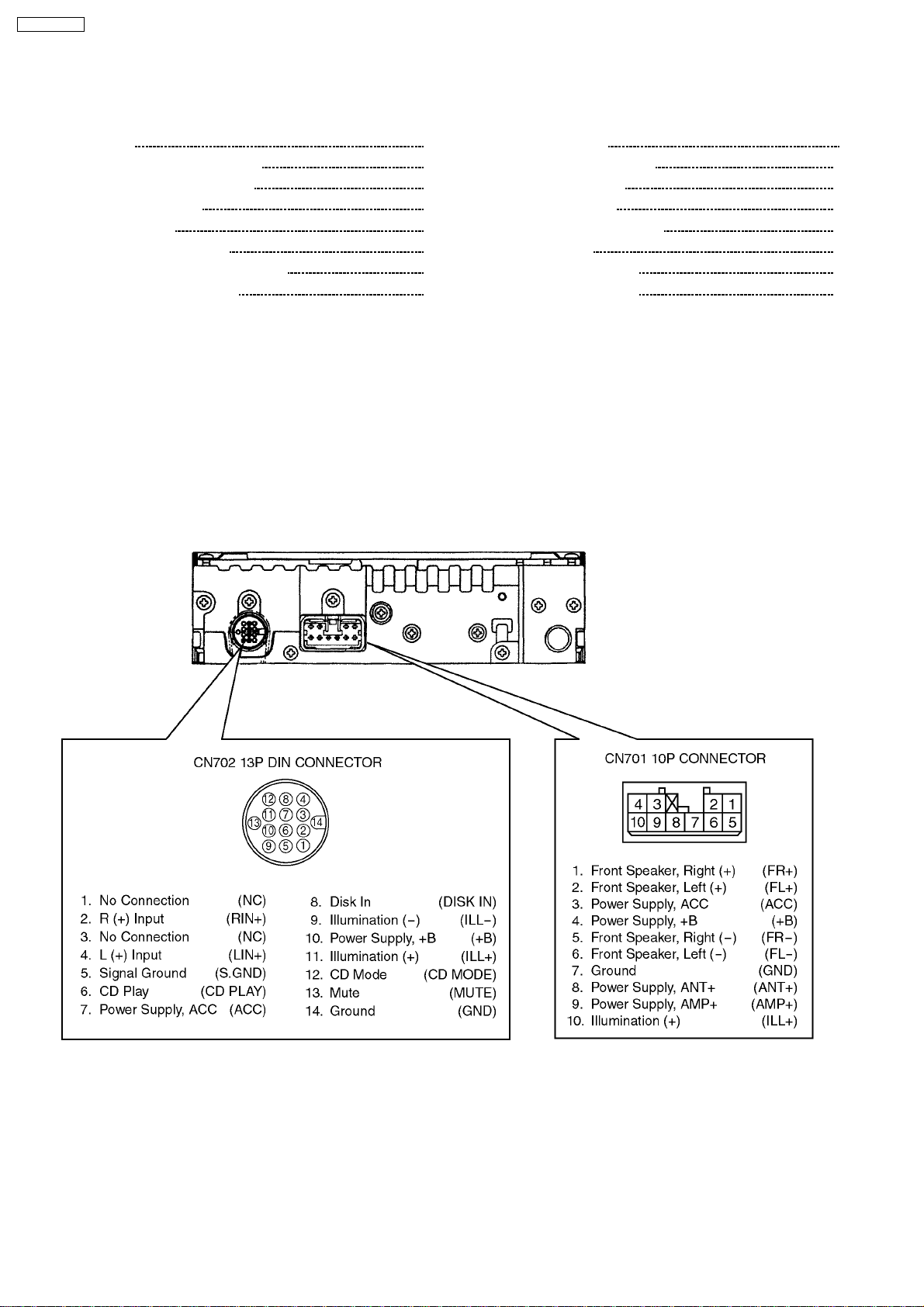
2 REAR VIEW AND CONNECTORS
2
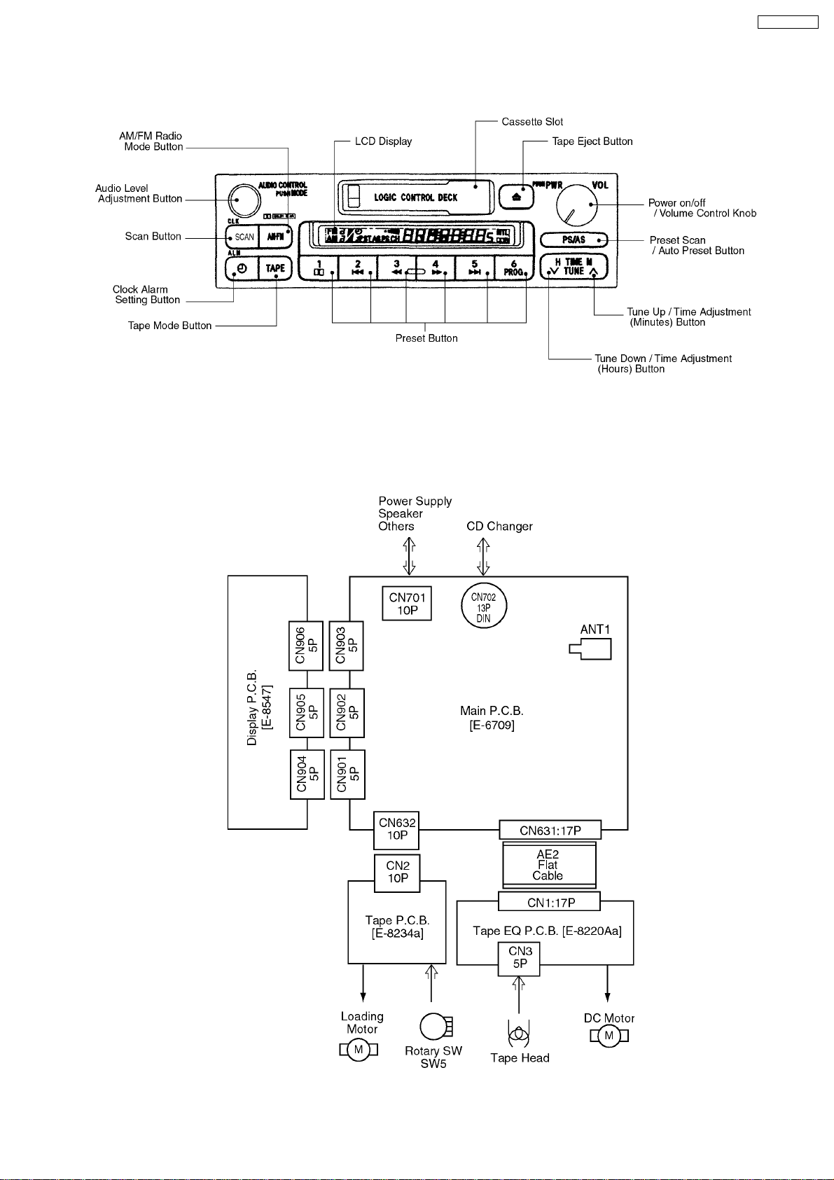
3 FRONT VIEW AND FUNCTIONS
CQ-DT6930ZE
4 WIRING CONNECTION
3
CQ-DT6930ZE
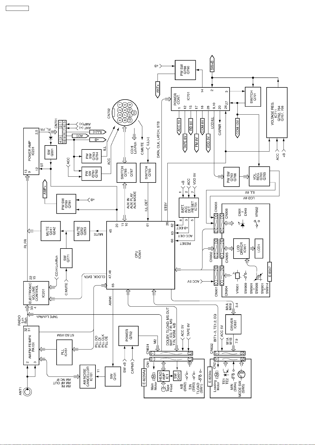
5 BLOCK DIAGRAM
4
6 TERMINALS DESCRIPTION
CQ-DT6930ZE
6.1. Main Block
IC601 : C2BBGE000295
Pin
No.
1 LCD-CL Clock for LCD data O 0
2 LCD-DI LCD data O 0
3 NC No connection - 4 GND Ground - 0
5 NC No connection - 6 NC No connection - 7 VDD +5V power supply - 5.0
8 NC No connection - -
9 AUX IN CD disc detection I 0
10 CD STOP CD stop O 0
11 CD ON CD power on O 0
12 NC No connection - 13 M1-B Tape main motor control O 0
14 M1-A Tape main motor control O 0
15,16- (Connecting tp ground) - 0
17 SEEK UP Not used - 18 SEEK DWN not used - 19 NC No connection - 20 AMP ON Ext. amp control O 3.8
21 LATH Data latch O 5.0
22 A/B Tape FF/REW switch I 0
23 /MTL Metal tape mode O 5.0
24 DATA Data for system power IC O 0
25 CLK Clock for system power IC O 0
26 STBY System power IC stand-by O 5.0
27 /MS TPS no sound detection I 0
28 MS PL/FF MS mode selection O 0
29 T.LOAD Tape loading detection I 0
30 /DOLBY Dolby control O 0
31 CAM-A/B Tape side detection I 5.0
32 /T.IN Tape insert detection I 0
33 GND Ground - 0
34 TE2 Tape end detection I 1.8
35 TE1 Tape end detection I 2.2
36,37DIV1,2 Not used - -
38 /M2F Tape solenoid control O 0.5
39 NC No connection - 40 MSM MS gain control O 0
41 /EQ Metal tape detection I 0
42 BIT3 Tape moe SW I 0
43 BIT2 Tape mode SW I 4.9
44 BIT1 Tape mode SW I 4.9
45 MUTE Mute O 0
46 BEEP Beep output O 0
47 VOL DAT Data for electronic vol. O 0
48 VOL CLK Clock for electronic vol. O 0
49 NC No connection - 50 TEST (+5V pull-up) - 4.2
51 DIV SW Not used - 52 PLL.DO PLL data I 4.9
53 PLL.CLK PLL clock O 0
54 PLL.DI PLL data O 0
55 PLL.CE PLL chip enabling O 0
56,57NC No connection - -
Port Description I/O (V)
62 +B-DET Battery level detection I 4.5
63 ACC-DET ACC level detection I 4.5
64 /T.EJECT Tape eject I 3.4
65 AN NK AM noise cancellation O 3.4
66 MODE B Encoder data input I 0
67 MODE A Encoder data input I 0
68 VDD +5V power supply - 4.9
69 X1 Crystal oscillatorv terminal - 2.4
70 X2 Crystal oscillatorv terminal - 0.6
71 GND Ground - 0
72 XT2 Crystal oscillatorv terminal - 2.6
73 XT1+ Crystal oscillatorv terminal - 2.3
74 AVDD +5V power supply - 5.0
75 ACC 5V +5V power supply - 5.0
76 VSM Radio signal level detection I 0
77 MAIN-VOL Main volume level I 0
78 AMSMTA AM radio signal level detection I 0
79 LCD-DO LCD data I 4.9
80 LCD-CE LCD driver enabling O 0
6.2. Display Block
IC601 : YEAMLC75853
Pin
No.
1-20 SEG1-20 LCD segment data O 2.6
21-33 - Not used - 34-40 SEG34-40 LCD segment data O 2.6
41-43 COM1-3 LCD common output O 2.6
44 S41 Not used - -
45-49 KS1-6 Key scan signal O 5.2
50 KI1 Not used - -
51-54 KI2-5 Key data input I 0
55 TEST (Connecting to ground) - 0
56 VDD +5V power supply - 5.2
57 VDD1 Ground through capacitor - 3.5
58 VDD2 Ground through capacitor - 1.8
59 VSS Ground - 0
60 OSC CR oscillator - 4.1
61 DO key data output O 5.2
62 CE Chip enable I 0
63 CLK LCD clock I 0
64 DI LCD data input I 0
Port Description I/O (V)
58 ST FM stereo detection I 0
59 SD B/S detection I 0
60 /RESET System reset I 4.5
61 /ILL-DET illumi. on detection I 3.5
5
CQ-DT6930ZE
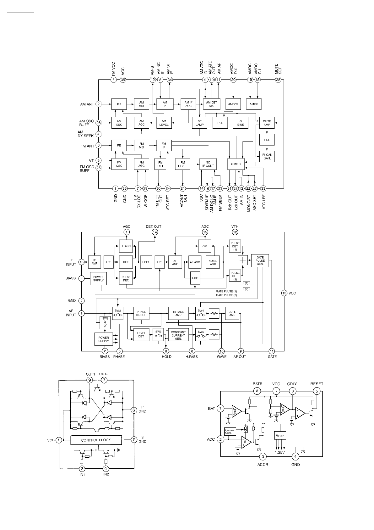
7 PACKAGE AND IC BLOCK DIAGRAM
7.1. Main Block
PA101 : YEP0PTA512B0
IC101 : YEAMHA12181F
IC631 : YEAMLB1930MT IC751 : AN8065SE1
6
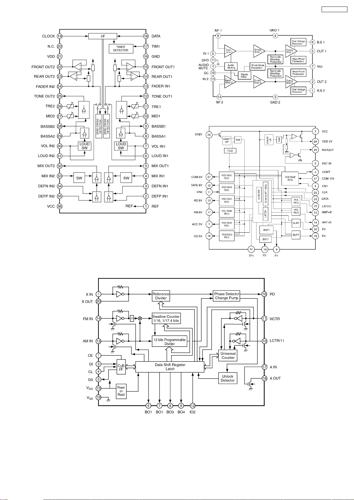
IC231 : YEAMLA4450
CQ-DT6930ZE
IC201 : YEAMM62435FA
IC701 : C0DBZHZ00005
IC451 : YEAMLC72135C
7
 Loading...