

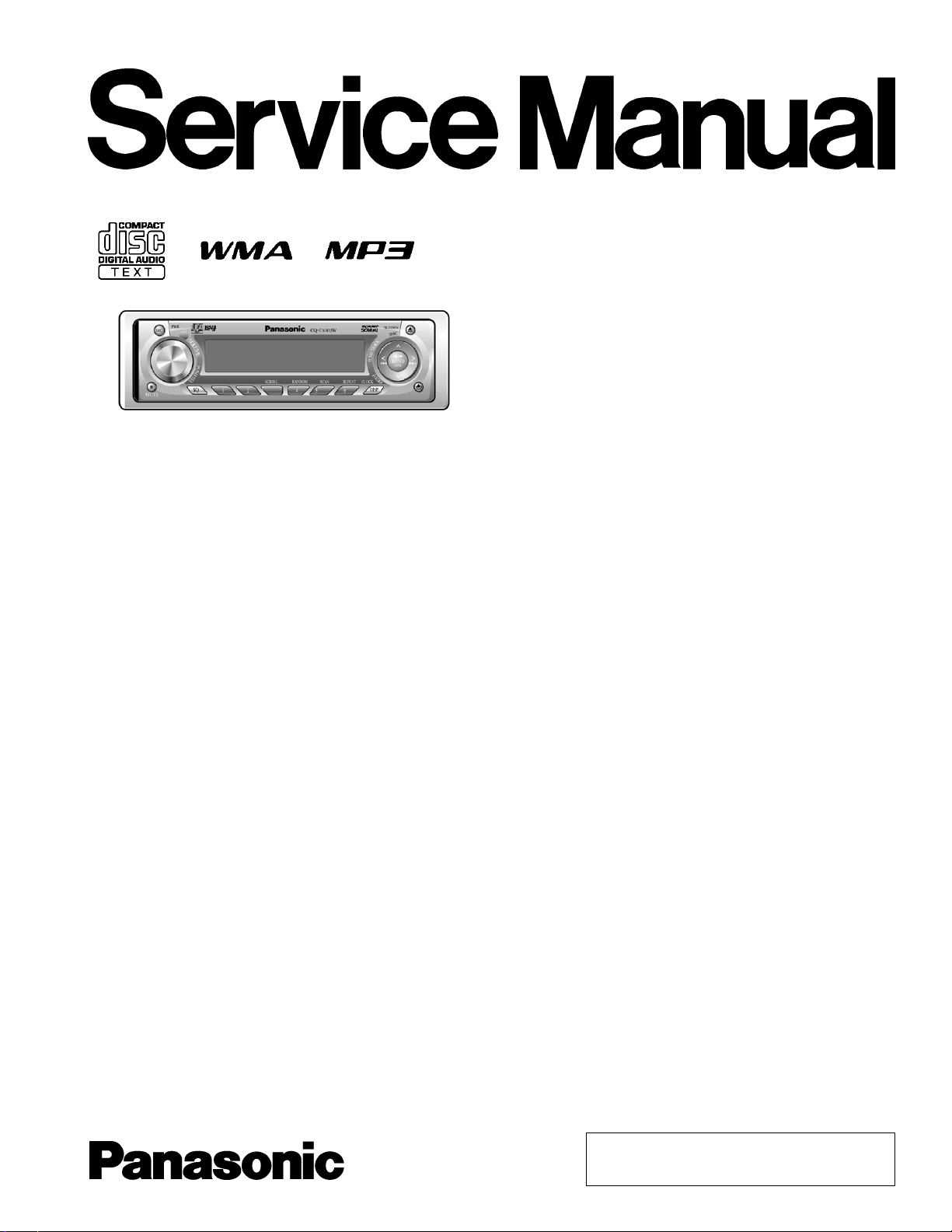
Panasonic CQC-5302-W Service manual
Specifications*
ORDER NO. ACED060610C3
AUTOMOTIVE AFTERMARKET
CQ-C5302W
WMA MP3 CD Player/Receiver with CD
Changer Control
General
Power Supply DC 12V (11V - 16V),
Test Voltage 14.4V
Negative Ground
Current Consumption Less than 2.2A (CD mode ; 0.5W
4-channels)
Maximum Power Output 50W×4 (at 1kHz)
Tone/SQ Adjustment Range SQ Low/Bass ; ±12dB
(at 60Hz, 80Hz, 100Hz, 200Hz)
SQ Mid ; ±12dB
(at 500Hz, 1kHz, 2kHz, 3kHz)
SQ High/Treble ; ±12dB
(at 10kHz, 12kHz, 15kHz, 18kHz)
Speaker Impedance 4-8Ω
Pre-Amp Output Voltage 2.5V (CD mode; 1kHz, 0dB)
Pre-Amp Output Impedance 200Ω
Subwoofer Output Voltage 2.5V
Subwoofer Output Impedance 200Ω
FM Stereo Radio
Frequency Range 87.5MHz - 108.0MHz
Usable Sensitivity 6dB/µV. (S/N 30dB)
Frequency Response 30Hz-15kHz (±3dB)
Alternate Channel Selectivity 75dB
Stereo Separation 35dB (1kHz)
Image Rejection Ratio 70dB
IF Rejection Ratio 100dB
Signal to Noise Ratio 62dB
AM Radio
Frequency Range 531kHz - 1,602kHz
Usable Sensitivity 28dB/µV (S/N 20dB)
CD Player
Sampling Frequency 8 Times Oversampling
DA Converter 1bit DAC System
Pick-Up Type Astigma 3-beam
Light Source Semiconductor Laser
Wave Length 790nm
Frequency Response 20Hz to 20kHz (±1dB)
Signal to Noise Ratio 96dB
Total Harmonic Distortion 0.01% (1kHz)
Wow and Flutter Below measurable limits
Channel Separation 75dB
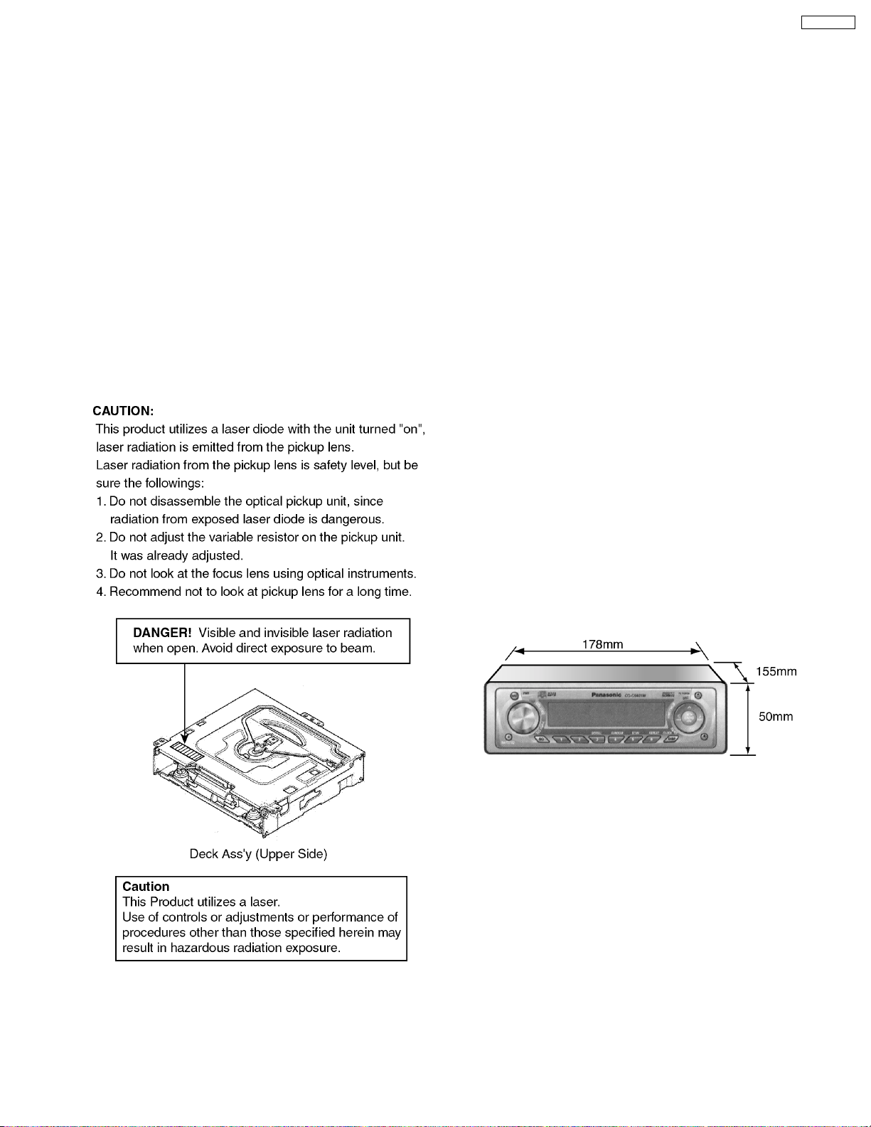
Dimensions** (W×H×D) 178×50×155mm
Weight** 1.6kg
* Specifications and the design are subject to possible modification
without notice due to improvements.
** Dimensions and Weight shown are approximate.
•
• Above specifications comply with EIA standards.
• •
© 2006 Matsushita Electric Industrial Co., Ltd. All
rights reserved. Unauthorized copying and
distribution is a violation of law.
CQ-C5302 W
CONTENTS
Page Page
1 ABOUT LEAD FREE SOLDER (PbF) 3
2 LASER PRODUCTS
3 FEATUERS
4 REPLACING THE FUSE
5 MAINTENANCE
6 NOTES
7 DIMENSIONS
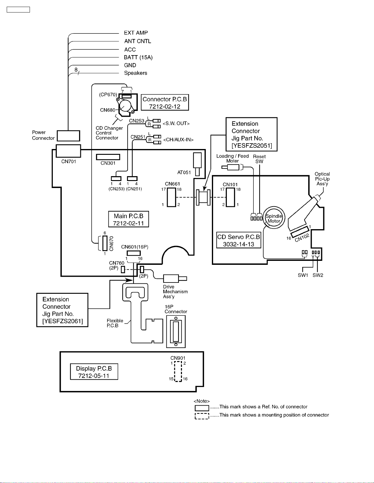
8 WIRING CONNECTION
9 DISASSEMBLY INSTRUCTIONS
10 TERMINALS DESCRIPTION
11 PACKAGE AND IC BLOCK DIAGRAM
3
3
12 REPLACEMENT PARTS LIST
3
13 EXPLODED VIEW (Unit)
14 CD PLAYER PARTS LIST
3
3
15 EXPLODED VIEW (CD Deck)
3
16 WIRING DIAGRAM
17 SCHEMATIC DIAGRAM
4
5
18 BLOCK DIAGRAM
8
11
14
19
20
23
24
29
33
2
CQ-C5302 W
1 ABOUT LEAD FREE
SOLDER (PbF)
Distinction of PbF PCB:
PCBs (manufactured) using lead free solder will have a PbF
stamp on the PCB.
Caution :
•
•
Pb free solder has a higher melting point than standard
• •
solder; Typically the melting point is 50 - 70°F (30 40°C) higher. Please use a soldering iron with
temperature control and adjust it to 700 ± 20°F (370 ±
10°C). In case of using high temperature soldering iron,
please be careful not to heat too long.
•
•
Pb free solder will tend to splash when heated too high
• •
(about 1100°F/600°C)
•
•
This lead free solder will be used for the products after
• •
serial No. 1,000,001.
2 LASER PRODUCTS
3 FEATUERS
•
•
Digital servo for reliable playback.
• •
•
•
PLL (Phase Locked Loop) synthesized tuning.
• •
•
•
18-FM, 6-AM presets with preset scan.
• •
•
•
Removable face plate.
• •
•
•
MP3/WMA Playback from CD-R/RW.
• •
•
•
CD Changer Control.
• •
4 REPLACING THE FUSE
Use fuses of the same specified rating (15amps). Using
different substitutes or fuses with higher ratings, or connecting
the product directly without a fuse, could cause fire or damage
to the stereo unit.
5 MAINTENANCE
Your product is designed and manufactured to ensure a
minimum of maintenance. Use a dry, a soft cloth for routine
exterior cleanin g. Never use benzine, thinner or other solvents.
6 NOTES
[RADIO BLOCK]
Do not align the AM/FM package block. When the package
block is necessary, it will be supplie d already aligned at the
factory.
[CD DECK BLOCK]
This model has no servo alignment points because
microcomputer controls the servo circuit.
7 DIMENSIONS
3
CQ-C5302 W
8 WIRING CONNECTION
4
9 DISASSEMBLY INSTRUCTIONS
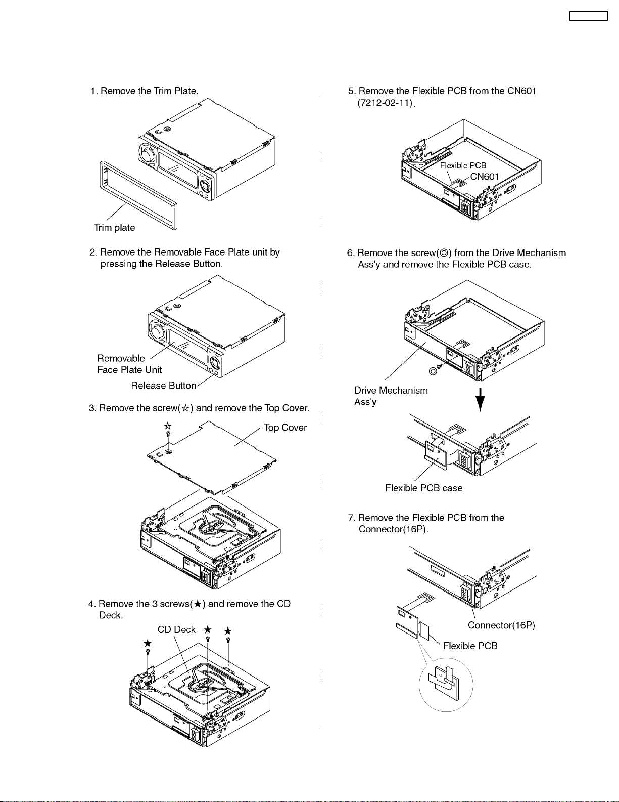
9.1. How to remove the Flexible PCB
CQ-C5302 W
5
CQ-C5302 W
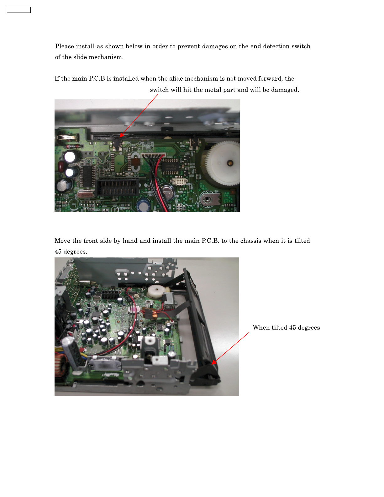
9.2. How to install the Main P.C.B of the Electric Slide Display
6
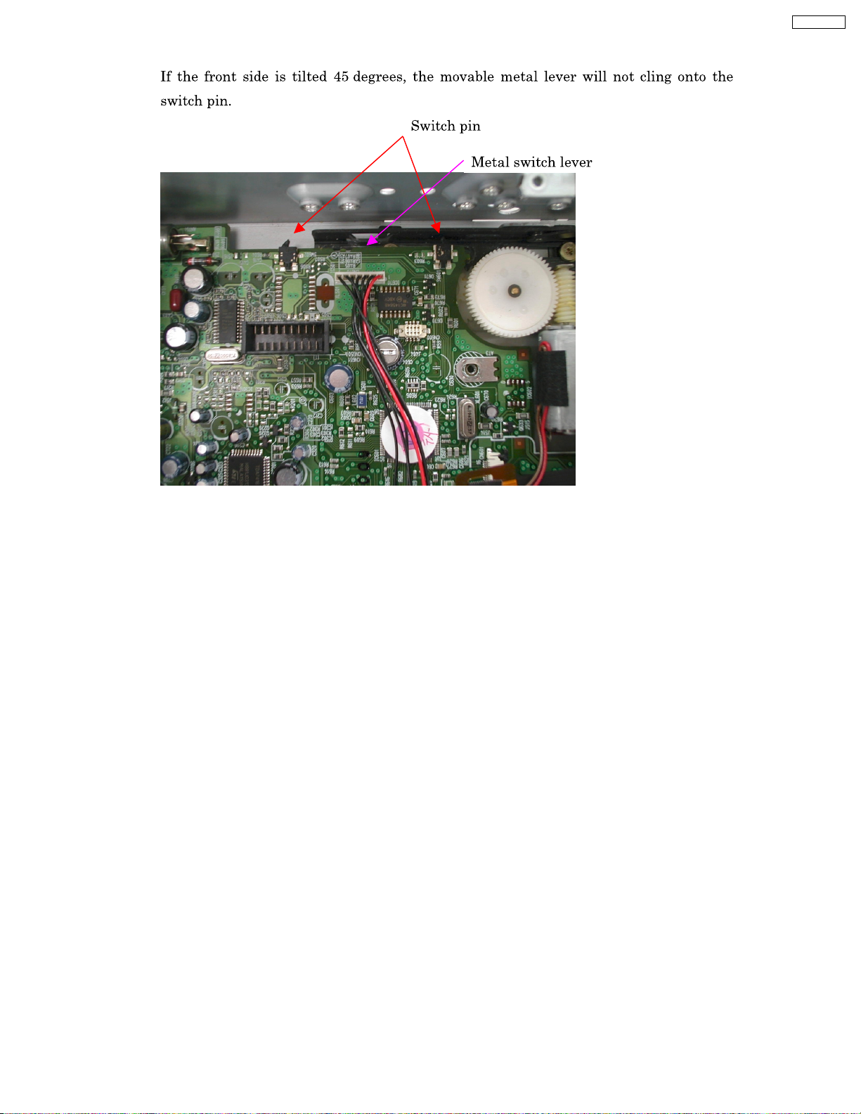
CQ-C5302 W
7
CQ-C5302 W
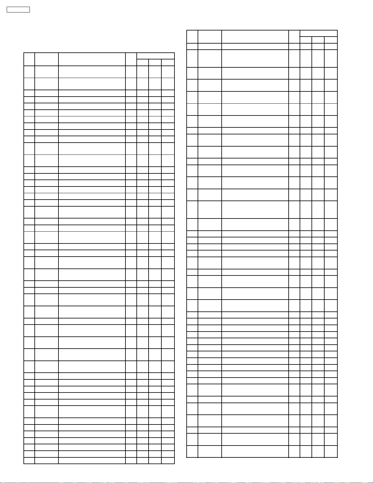
10 TERMINALS DESCRIPTION
10.1. Main Block
IC601 : YESAM288
Pin
Port Description I/O Volt (V)
No.
1 PANEL
OPEN
2 PANEL
CLOSE
3 LCD DI LCD data O 4.7 4.7 4.7
4 BATT BATT detection I 5.1 5.1 5.1
5 ACC ACC detection I 5.1 5 5.1
6 SDA Electronic VOL data I/O 5 5 5
7 SCK Electronic VOL clock O 5 0 5
8 LCD DO LCD data I 4.9 4.9 4.9
9 Vss GND - 0 0 0
10 ST FM ST detection I 5.1 5.1 5.1
11 PLL DI
(MO)
12 PLL DO
(MI)
13 PLL CLK PLL clock output O 5 5 5
14 PLL CE PLL chip enable output O 0 0 5
15 CD RST CD deck reset output O 5 5 0
16 XM RX XM tuner RX data O 4.8 4.8 4.8
17 LCD CLK LCD clock O 4.9 4.9 4.9
18 XM TX XM tuner TX data I 0 0 0
19 CD SO
(MI)
20 CD SCK CD clock transmit O 4.9 4.9 4.9
21 Vdd Power supply I 5 5 5
22 CD SI
(MO)
23 NC No Connection - - - 24 CDC CLK CD Changer clock I 0 0 0
25 CONDEN
SOR
26 CDC
DATA
27 CDC STB Changer storobe signal input I 0 0 0
28 CD IN DISC In detection I 4.9 4.9 0.4
29 DECK V
CONT
30 CD STB Strobe signal for CD
31 NC No Connection - - - 32 Avdd Power supply of D/A
33 AVREF Reference voltage for D/A
34 AVGND Reference GND for D/A
35 AVSS GND for A/D and D/A
36 SD FM/AM signal strength I 0.3 0 0.3
37 INIT A Initializ A I 0 0 0
38 INIT B Initializ B I 0 0 0
39 AIN SPE.ANA A.IN I 0 0 0
40 Vss GND I 0 0 0
41 CD A0 Signal output according to
42 NC No Connection - - - 43 NC No Connection - - - 44 NC No Connection - - - 45 CD SW1 CD mechanism switch I 0 0 0
46 CD SW2 CD mechanism switch I 5 5 0
47 MOD0 Operating mode input 0 I 5.2 5.2 5.2
48 MOD1 Operating mode input 1 I 5.1 5.1 5.1
PANEL OPEN detection I 5.2 5.2 5.2
PANEL CLOSE detection I 0 0 0
PLL data output O 0 0 0
PLL data input I 5.2 5.2 5.2
CD Data I 1.4 1.4 1.4
CD Data O 0 0 0
Capacitor for power supply - 3.2 3.2 3.2
CD Changer data I 0 0 0
DECK power supply control
output
communication
converter
converter
converter
converter
command employmen t
FM AM CD
O 5 5 5
O 3.3 3.3 3.3
I 5.1 5.1 5.1
I 5.1 5.1 5.1
I 0 0 0
I 0 0 0
O 0 0 5.1
Pin
Port Description I/O Volt (V)
No.
49 MOD2 Operating mode input 2 I 0 0 0
50 H
STANDB
Y
51 DC DC
CNT (NC)
52 FP
MOTOR1
53 FP
MOTOR2
54 V CNT1 Panel driving voltage control1O 0 0 0
55 V CNT2
(NC)
56 SA CLK Spectrum analizer clock O 5 4.9 4.9
57 EXT
MUTE
58 AMP
CONT
59 BZ-OUT Buzzer output O 0 0 0
60 ANT
CONT
61 DIM1
(NC)
62 DIM2
(NC)
63 CDC
REM
OUT
64 CDC
SENS
65 CDC 1/2 CDC 1/2 change output O 0 0 0
66 NC - - - - 67 REMO IN Main wake-up request I 4.9 4.9 4.9
68 NC - - - - 69 RDS CLK
(NC)
70 NC - - - - 71 RD DATA
(NC)
72 MAIN
CONT
73 INV
CONT
74 AF MUTE AF MUTE control O 5.1 5.1 5.1
75 RESET Reset input I 5.1 5.1 5.1
76 NC No Connection - - - 77 NC No Connection - - - 78 NC - I 0 0 0
79 Vss GND I 0 0 0
80 X1 Crystal oscillator input I 2.1 2.1 2.1
81 X2 Crystal oscillator output O 2.5 2.5 2.5
82 Vdd Power supply I 5.1 5.1 5.1
83 P00 Pldaun port for writing I 0 0 0
84 P01 Pull-up port for writing I 5.1 5.1 5.1
85 OFFSET
DET
86 STBY PWR-IC STBY control output O 5.1 5.1 5.1
87 AMP
MUTE
88 ILL SENS
(NC)
89 NC - - - - 90 EP DO
(MI) (NC)
91 EP D0
(M0) (NC)
External standby input I 5.1 5.1 5.1
- - - - -
Front open/close control 1 O 5 5 5
Front open/close control 2 O 5 5 5
- - - - -
TEL/NAVI MUTE input I 5.4 5.4 5.4
External AMP control O 5 5 5
Motor antenna control O 5 5 0
- - - - -
- - - - -
Remote control data for CD
Changer
CDC 1/2 detection I 5.1 5.1 5.1
- - - - -
- - - - -
MAIN power supply control O 5 4.9 4.9
INV power supply control O 5.1 5 5
PWR-IC offset detection I 0 0 0
PWR-IC MUTE control output O 0 0 0
- - - - -
- - - - -
- - - - -
FM AM CD
O 5 5 5
8
Pin
Port Description I/O Volt (V)
No.
92 EP SK
(NC)
93 SUB W U
REQ/
LCD CE
94 DISPM
CNT
95 EJE ILL
(NC)
96 Rotary 1 Rotary Encoder 1 I 4.9 5 5
97 Rotary 2 Rotary Encoder 2 I 4.9 4.9 5
98 S LED Security LED control output O 0 0 0
99 PANELINPANEL detect I 5.3 5.3 5.3
100 EP CS
(NC)
Sub Wake-up request O 0 0 0
Power supply control for
display
- - - - -
- - - - -
- - - - -
FM AM CD
O 0 0 0
10.2. Display Block
IC901 : YESAM168
Pin No. Port Description I/O (V)
1-35 SEG3-37 LCD segment data O 2.5
36-51 SEG40-55 LCD segment data O 2.5
52-55 COM1-4 LCD common O 2.5
56,57 SEG39,38 Not used - 58-61 KS3-6 Key scan O 5.0
62-66 Kl1-5 Key data I 0
67 VDD +5V power supply - 5.0
68 VLCD VLCD terminal - 4.8
69 VLCD1 VLCD1 terminal - 3.3
70 VLCD2 VLCD2 terminal - 1.7
71 VSS Ground - 0
72 TEST (Connecting to ground) - 0
73 OSC Oscillator terminal - 3.9
74 RESET Reset I 4.8
75 DO Key data output O 5.0
76 CE LCD driver chip enable I 0
77 CLK LCD clock I 4.9
78 DI LCD data I 4.9
79,80 SEG1,2 LCD segment data O 2.5
10.3. CD Servo Block
IC401 : YESAM348
Pin
No.
Port Descriptions I/O (V)
1 CVSS1 GND - 0
2 - - - 3 CVSS2 GND - 0
4 DVDD1 I/O system (3.3V) power supply - 3.3
5 A10 Address bus of FLASH ROM O 0
6 - - - 7 A11 Address bus of FLASH ROM O 3.3
8 A12 O 3.3
9 A13 O 3.3
10 A14 O 3.3
11 A15 O 3.3
12 /CVDD1 CORE CPU system (1.6V) power
supply
13 - - - 14 DVSS1 GND - 0
15 CVSS3 GND - 0
16 /CVDD2 I/O system (3.3V) power supply - 1.6
17 - - - 18 - - - 19 READY - - 3.3
20 /PS FLASH ROM selection signal O 3.3
21 - - - 22 - - - 23 R/W Lead/light signal to FLASH ROM O 3.3
24 /MSTRB Memory access signal O 3.3
25 - - - 26 /MSC - - 3.3
27 MUTE Mute signal output (H:Mute on) O 0
28 - - - 29 - - - 30 /HOLD - - 3.3
31 BIO SUBO input I 0
32 MP/MC Operation mode setting (external pull-
up)
33 DVDD2 I/O system (3.3V) power supply - 3.3
34 CVSS4 GND - 0
35 BD R1 GND I 0
36 - - - 37 CVSS5 GND - 0
38 - - - 39 - - - 40 DVSS2 GND - 0
41 CLK C M AUDIO bit clock input I 1.6
42 SCK Clock input I 3.3
43 LRCK CMAUDIO L/R identifying signal input I 1.6
- 1.6
I 3.3
CQ-C5302 W
44 CDFS Serial frame sink signal input I 2.6
45 DATACMAUDIO serial data input I 1.6
46 - - - 47 SI Serial data input I 0
48 CLK M C AUDIO bit clock output O 1.6
49 SCK Clock input I 3.3
50 CVSS6 GND - 0
51 - - - 52 CVDD3 CORE CPU system (1.6V) power
supply
53 LRCK MCAUDIO L/R identifying signal output O 1.6
54 CDFS Serial frame sink signal input I 2.4
55 - - - 56 DVDD3 I/O system (3.3V) power supply - 3.3
57 DVSS3 GND - 0
9
- 1.6
CQ-C5302 W
Pin
Port Descriptions I/O (V)
No.
58 RESTSWMechanics deck REST SW input I 3.3
59 DATA MCAUDIO serial data output O 1.6
60 SO Serial data output O 1.2
61 - - - 62 - - - 63 /NMI - - 3.3
64 /INT0 - - 3.3
65 /INT1 - - 3.3
66 BLKCK Subcode block clock pulse input I 0
67 /INT3 - - 3.3
68 CV DD4 CORE CPU system (1.6V) power
- 1.6
supply
69 SW1 Mechanics deck SW1 input I 0
70 CVSS7 GND - 0
71 MCLK Clock output (To Servo DSP) O 3.3
72 DVSS4 GND - 0
73 MLD Command load signal output (To
I 3.3
Servo DSP)
74 MDATA Command data output (To Servo
O 3.3
DSP)
75 DVDD4 I/O system (3.3V) power supply - 3.3
76 DVSS5 GND - 0
77 CLK MD1 Clock mode setting (L fixation) I 0
78 CLK MD2 Clock mode setting (H fixation) I 3.3
79 CLK MD3 Clock mode setting (L fixation) I 80 - - - 81 SW2 Mechanics deck SW2 input I 0
82 - - - 83 EMU0 - - 0
84 EMU/OF
- - 3.3
F
85 TDO - - 3.3
86 TDI - - 0
87 /TRST - - 3.3
88 TCK - - 0
89 TMS - - 3.3
90 CVSS8 GND - 3.3
91 CVDD5 CORE CPU system (1.6V) power
- 0
supply
92 HPIENA GND I 1.6
93 DVSS6 GND - 0
94 - - - 95 CLKENA Oscillation output Cainabl signal O 3.3
96 X1 Crystal Connection O 0
97 X2/CLKIN Crystal Connection I 0
98 RS Reset signal input I 1
99 D0 Data base of FLASH ROM I/O 3.4
100 D1 I/O 0
101 D2 I/O 0
102 D3 I/O 0
103 D4 I/O 0
104 D5 I/O 0
105 A16 Address bus of FLASH ROM O 0
106 DVSS7 GND - 0
107 A17 Address bus of FLASH ROM O 3.3
108 A18 O 0
109 A19 Address bus of FLASH ROM O 0
110 A20 O 0
111 CVSS9 GND - 0
112 DVDD5 I/O system (3.3V) power supply - 3.3
113 D6 Data bus of FLASH ROM I/O 0
114 D7 I/O 0
115 D8 I/O 0
116 D9 I/O 0
117 D10 I/O 0
Pin
Port Descriptions I/O (V)
No.
118 D11 Data bus of FLASH ROM I/O 0
119 D12 I/O 0
120 STAT Status signal input I 0.4
121 D13 Data path of FLASH ROM I/O 0
122 D14 I/O 0
123 D15 I/O 0
124 - - - 125 CVDD6 CORE CPU system (1.6V) power
- 1.6
supply
126 CVSS10 GND - 0
127 - - - 128 DVSS8 I/O system (3.3V) power supply - 0
129 - - - 130 DVDD6 I/O system (3.3V) power supply - 3.3
131 A0 Address bus of FLASH ROM O 0
132 A1 O 0
133 A2 O 3.3
134 A3 O 3.3
135 /RST Reset signal output (To Servo DSP) O 3.3
136 A4 Address bus of FLASH ROM O 3.3
137 A5 O 0
138 A6 O 3.3
139 A7 O 3.3
140 A8 O 0
141 A9 O 3.3
142 CVDD7 CORE CPU system (1.6V) power
- 1.6
supply
143 - - - 144 DVSS9 GND - 0
10
11 PACKAGE AND IC BLOCK DIAGRAM
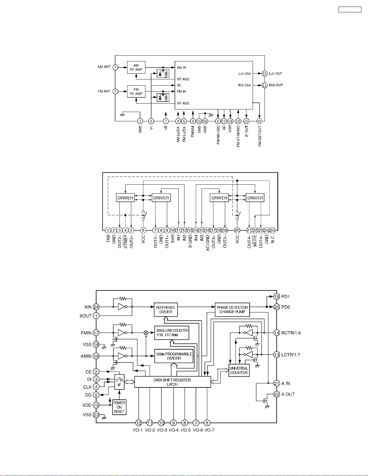
11.1. Main Block
PA051 : YESAP413
CQ-C5302W
IC271 : YESAM274
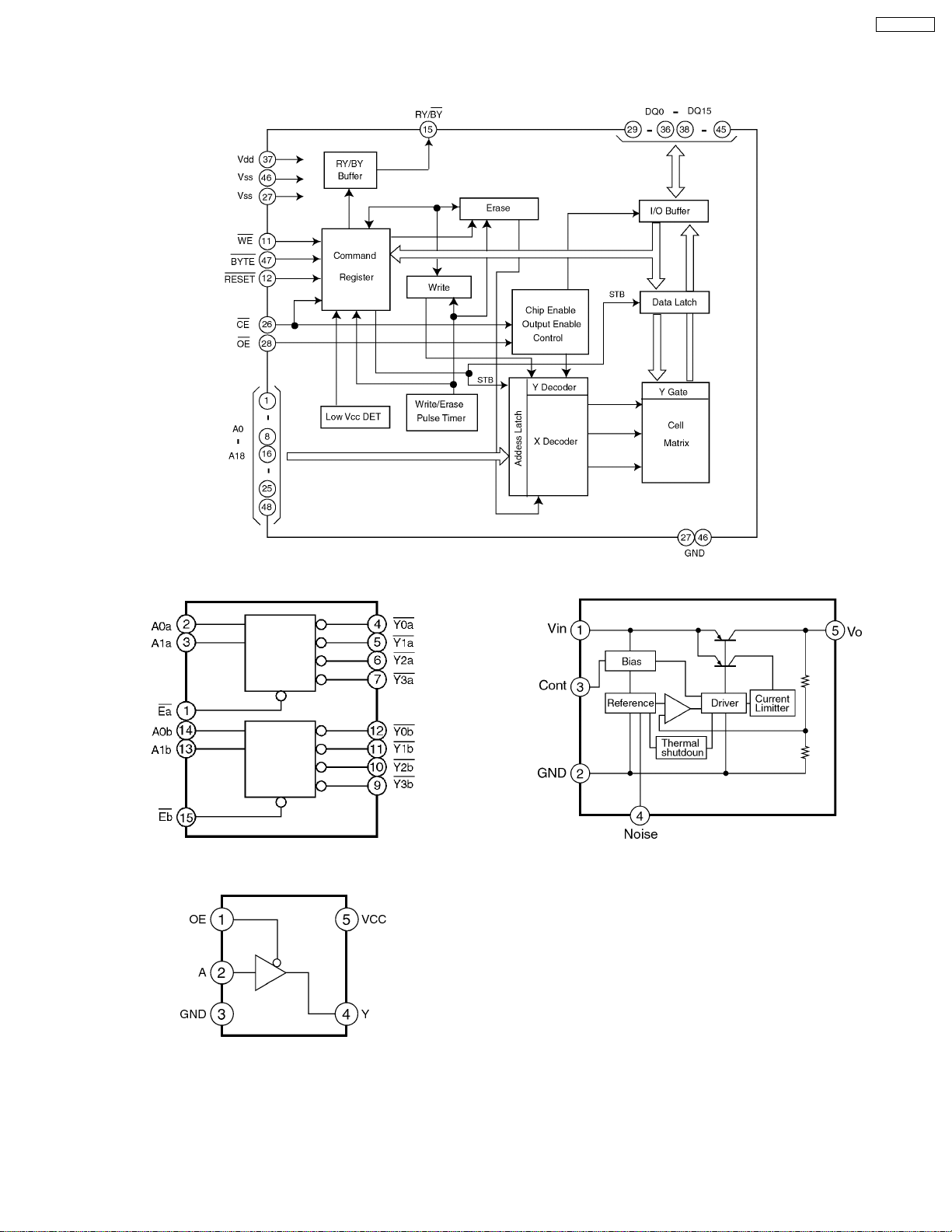
IC401 : YESAM284
11
CQ-C5302W
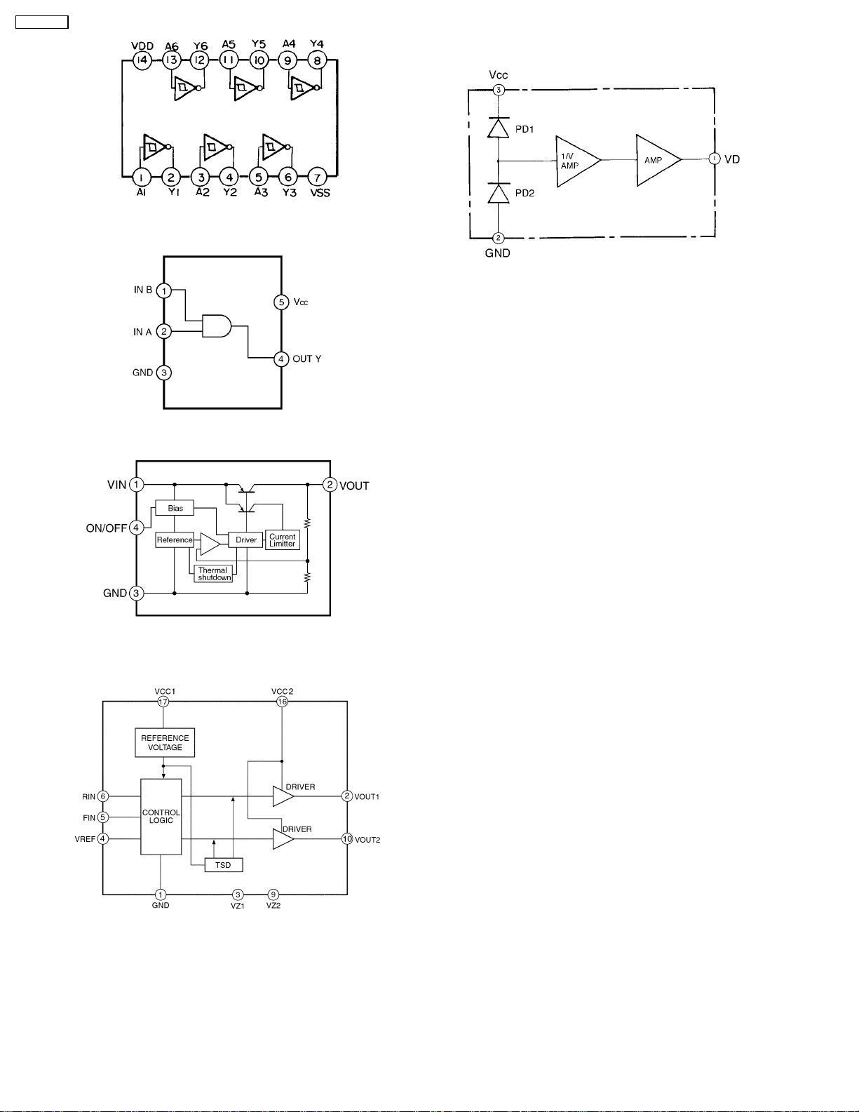
11.2. Display Block
IC650 : YESAM265
IC902 : YESAM264
IC681 : YESAM273
IC750 : YESAM267
IC760 : YESAM287
12
11.3. CD Servo Block
CQ-C5302 W
IC403 : YESAM171
IC402 : YESAM353
IC404 : YESAM178
IC405 : YESAM270
13
 Loading...