

Panasonic CQ-C3405U Service Manual
ORDER NO. ACED061222C7
AUTOMOTIVE AFTERMARKET
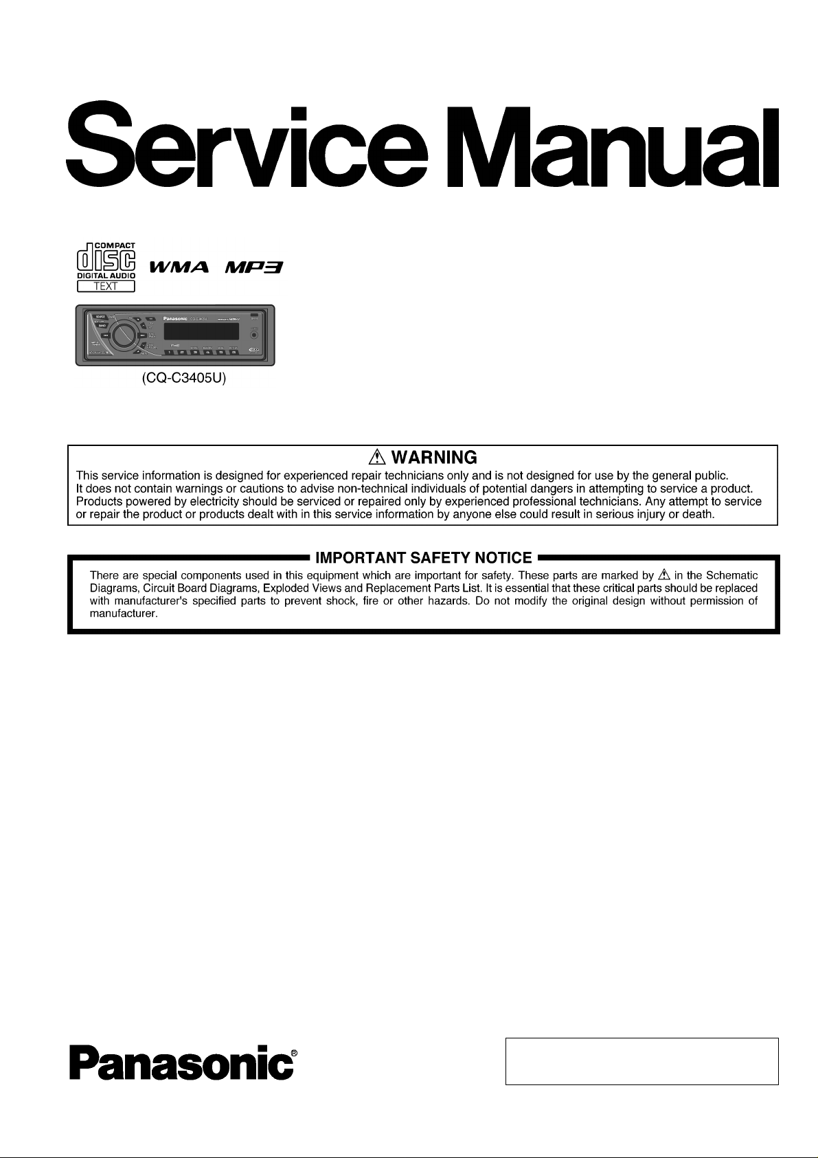
CQ-C3405U
CQ-C3305U
WMA MP3 CD Player/Receiver
C4
TABLE OF CONTENTS
PAGE P AGE
1 Service Navigation ----------------------------------------------- 2
2 Specifications ----------------------------------------------------- 3
3 Features ------------------------------------------------------------- 4
4 T ec hnic al Desc ri ptions----------------------------------------- 5
5 Block Diagram----------------------------------------------------- 8
6 Wiring Connection Diagram---------------------------------11
7 Schematic Diagram---------------------------------------------12
8 Schematic Diagram-2------------------------------------------15
9 Printed Circuit Board-------------------------------------------17
10 Exploded View and Replacement Parts List -----------21
11 Schematic Diagram for Printing with Letter Size-----37
© 2006 Matsushita Electric Industrial Co., Ltd. All
rights reserved. Unauthorized copying and distribution is a violation of law.
1 Service Navigation
1.1. About Lead Free Solder (PbF)
Distinction of PbF PCB :
• PCBs (manufactured) using lead free solder will have a Pb F
stamp on the PCB.
Caution :
• Pb free solder has a higher melting point than standard solder; Typically the melting point is 50 - 70°F (30 - 40°C)
higher. Please use a soldering iron with temperature control
and adjust it to 700 ± 20°F (370 ± 10°C). In case of using
high temperature soldering iron, please be careful not to
heat too long.
• Pb free solder will tend to splash when heated too high
(about 1100°F/600°C)
• This lead free solder will be used for the products after serial
No. 1,000,001.
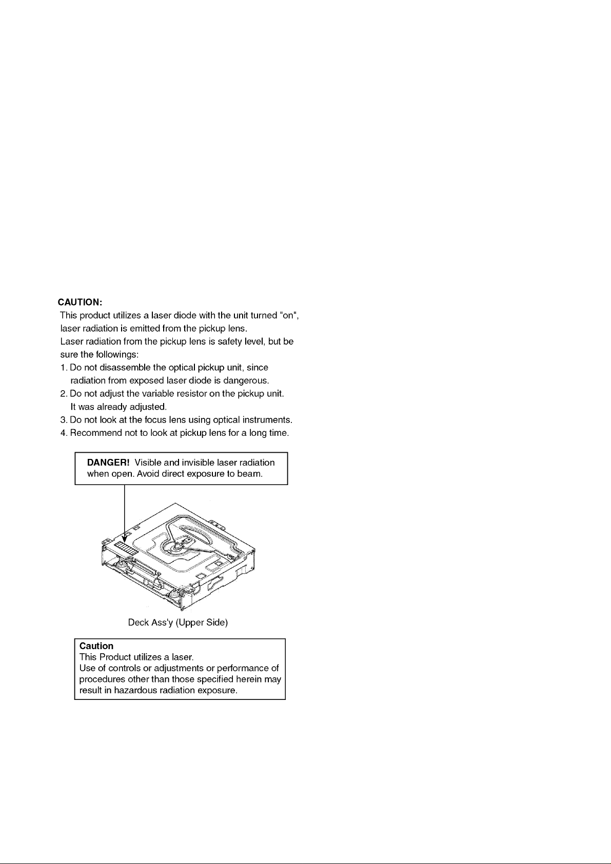
1.2. Laser Products
1.4. Maintenance
Your product is designed and manufactured to ensure a minimum of maintenance. Use a dry, a soft cloth for routine exterior
cleaning. Never use benzine, thinner or other solvents.
1.5. Notes
[RADIO BLOCK]
Do not align the AM/FM package block. When the package
block is necessary, it will be supplied alrea dy alig ned at the factory.
[CD DECK BLOCK]
This model has no servo alignment points because microcomputer controls the servo circuit.
1.3. Replacing the Fuse
Use fuses of the same s pe cif ied rati ng 15 a mps. Using different
substitutes or fuses with higher ratings, or connecting the unit
directly without a fu se, could cause fire or damage to th e st ere o
unit.
2
2 Specifications
2.1. Specifications*
General
Power Supply DC 12V (11V - 16V)
Current Consumption Less than 2.1A (CD mode, 0.5W 4-
Maximum Power Output 50W × 4 (at 1kHz), volume control maxi-
Tone Adjustable Range Bass:±12dB (at 100 Hz),
Speaker Impedance 4 - 8 Ω
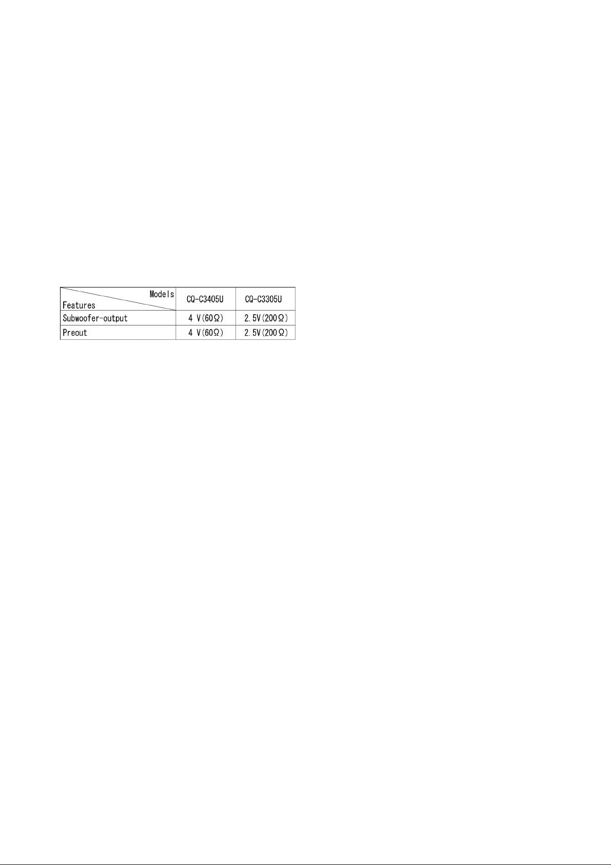
Pre-amp Output Voltage 4 V (CQ-C3405U), 2.5 V (CQ-C3305U)
Subwoofer output Voltage
Pre-amp Output Voltage 60 Ω (CQ-C3405U), 200 Ω (CQ-C3305U)
Subwoofer output Voltage
Front AUX Input
Input Impedance
Allowable External
Input
Connector
Test Voltage 14.4V
Negative Ground
Speaker)
mum
Treble: ±12 dB (at 10kHz)
(CD mode: 1 kHz, 0 dB)
4 V (CQ-C3405U), 2.5 V (CQ-C3305U)
(CD mode: 1 kHz, 0 dB)
60 Ω (CQ-C3405U), 200 Ω (CQ-C3305U)
10 kΩ
2.0 V
3.5 mm Stereo mini-pin
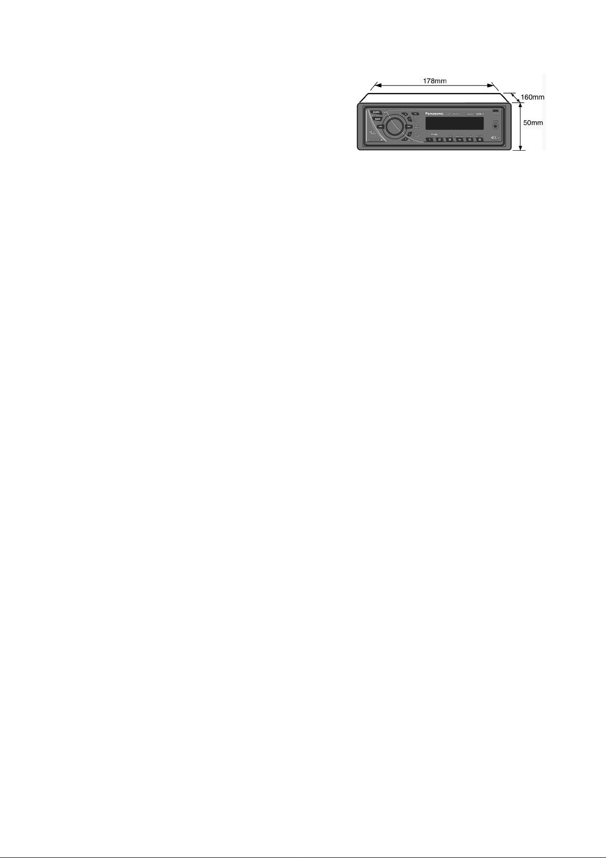
2.2. Dimensions
Dimensions (W×H×D)** 178×50×160mm (7”×1-5/16"×6-5/16")
Weight** 1.3 kg (2 lbs. 14 oz)
CD Player
Sampling Frequency 8 times oversampling
DA Converter 1 bit DAC System
Pick-Up Type Astigma 3-beam
Light Source Semiconductor Laser
Wave Length 790 nm
Frequency Response 20 Hz - 20 kHz (±1 dB)
Signal to Noise Ratio 96 dB
Total Harmonic Distortion
Wow and Flutter Below Measurable Limits
Channel Separation 75 dB
Stereo Radio
FM
Frequency Range 87.9 MHz - 107.9 MHz
Usable Sensitivity 10.2 dBf (0.9 µV, 75 Ω)
50 dB Quieting Sensitivity
Frequency Response 30 Hz - 15 kHz (±3 dB)
Alternate Channel Selectivity
Stereo Separation 35 dB (at 1 kHz)
Image Rejection Ratio 55 dB
IF Rejection Ratio 100 dB
Signal to Noise Ratio 62 dB
AM
Frequency Range 530 kHz - 1710 kHz
Usable Sensitivity 27 dB/µV (22µV, S/N 20 dB)
0.01 % (1 kHz)
15.2 dBf (1.6 µV, 75Ω)
75 dB
* Specifications and the design are subject to possible modification
without notice due to improvements.
** Dimensions and Weight shown are approximate.
** Above specifications comply with EIA standards.
3
3 Features
• Hands Free Phone System. (The optional Bluetooth handsfree kit: CY-BT100U)
• Expansion Module (The optional Hub unit: CY-EM100U).
• The optional adapter allows you to connect the optional
Panasonic CD changer unit (CX-DP880 U ).
• The optional adapter allows you to connect the optional
iPod® series.
• XM Satellite Radio. (The optional XM receiver: XMD1000)
• Sirius Satellite Radio. (The optional Sirius Satellite receiver:
SIR-PAN1)
• SQ (Sound Quality).
• The AUX Input terminal is equipped on the front panel.
• MP3/WMA Playback from CD-R/RW.
• Anti-Theft System.
• This manual is for 2 models CQ-C3405U and CQ-C3305U.
The following table describes the differences between 2
models.
4
4 Technical Descriptions
4.1. Terminals Description
4.1.1. Main Block
IC601 : YESAM389
Pin NoPort Description I/O Vol [V]
FM AM CD
1 DBGP0 Not connected - - - 2 DBGP1 Not connected - - - 3 DBGP2 Not connected - - - 4 RDS CLK Not connected - - - 5 RM DATA Remote control data I 4.8 4.8 4.8
6 CDC STB/
SYSID4
7 EVENT Hub event detection I 0 0 0
8 RESET System reset I 4.8 4.8 4.8
9 XT1 Crystal oscillator 1
10 XT2 Crystal oscillator 2
11 VSS Ground - 0 0 0
12 CF1 Ceramic oscillator 1
13 CF2 Ceramic oscillator 2
14 VDD +5V power supply - 5.0 5.0 5.0
15 INT A Pulled up for CQ-C3405U;
16 VSM Signal meter intensity
17 INT B Pulled down to GND - 0 0 0
18 LEVEL Audio level detection from
19 INT C Not connected - - - 20 ACC ACC level detection I 5.0 5.0 5.0
21 SYSID1 Hub connection device
22 SYSID2 Hub connection device
23 N.C. Not connected - - - 24 CDC DATA Serial data from CD
25 CDC CLK/
SYSID3
26 CD DI (CD
SI)
27 CD DO (CD
SO)
28 CD CLK Serial clock for CD O 4.7 4.7 4.7
29 CD CE (FS) CD chip enable O 0 0 1.6
30 CD MUTE CD mute I 0.2 0.2 5.0
31 CD RESET CD reset O 4.8 4.8 4.8
32 POWER
CNT
33 SUB
READY
34 REG
READY
35 CD SW1 CD detection switch 1 I 0 0 0
36 CD SW2 CD detection switch 2 I 0 0 0
37 CD MUTE Mute for Pick-up driver O 0 0 5.0
38 CD S/L Sleding/Loading mode
39 VSS Ground - 0 0 0
CD changer Strobe; or
Hub connection device
identification 4
(32.768kHz)
(32.768kHz)
(13.5MHz)
(13.5MHz)
Pulled down for CQC3305U
(Tuner)
Audio signal processor
identification 1
identification 2
changer
Serial clock for CD
changer; or Hub connection device identification 3
Serial data from CD I 0 0 4.8
Serial data to CD O 5.0 5.0 3.5
System power supply control
Sub ready from CD servo I 5.0 5.0 4.7
Reg. ready from CD servo I 5. 0 5.0 0
switch
I000
I 1.0 1.0 1.0
O 1.4 1.4 1.4
I 1.4 1.4 1.4
O 1.3 1.3 1.3
I 5.0 5.0 5.0
I 0.2 0 0.2
I000.3
I 4.9 4.9 4.9
I 4.9 4.9 4.9
I000
I000
O 5.0 5.0 5.0
O 5.0 5.0 5.0
Pin NoPort Description I/O Vol [V]
FM AM CD
40 VDD +5V power supply - 5.0 5.0 5.0
41 CD ERROR CD error status I 0 0 0
42 CD LIMIT SWCD limit detection switch I 5.0 5.0 5.0
43 CD EM Ejecting mode for Sled
44 CD LM Loading mode for Sled
45 HUB ACC
CNT
46 HUB CNT Hub connection check
47 INV CNT Not connected - - - 48 USB CNT Not connected - - - 49 LCD DI Serial data to LCD O 4.8 4.8 4.8
50 LCD DO Serial data from LCD I 4.8 4.8 4.8
51 LCD CLK Serial clock for LCD O 5.0 5.0 5. 0
52 LCD CE Chip enable for LCD CPU O 0 0 0
53 E-VOL I2C
DATA
54 E-VOL I2C
CLK
55 VDD +5V power supply - 5.0 5.0 5.0
56 VSS Ground - 0 0 0
57 E-VOL LV
CLK
58 E-VOL LV
DATA
59 STBY Standby mode for Power
60 SRS MODE 1Not connected - - - -
61 SRS MODE 2Not connected - - - -
62 SRS MODE 3Not connected - - - -
63 SRS
FOCUS
ELVL
64 EJ ILL Ejection key illumination
65 PANEL IN F ront panel detection I 0 0 0
66 LCD 5V
CNT
67 N.C. Not connected - - - 68 EJECT Ejection switch I 5.0 5.0 5.0
69 BATT Batt ery level detection I 5.0 5.0 5.0
70 EXT MUTE Telephone mute I 5.0 5.0 5.0
71 OP/CL Open/Close detection for
72 MODE B
(ROTARY
2)
73 MODE A
(ROTARY
1)
74 CDC REM
OUT
75 HUB-TX Transmission data to Hub O 0 0 0
76 HUB-RX Reception data from Hub I 0 0 0
77 USB TX Not connected - - - 78 USB RX Not connected - - - 79 FM MODE Power supply control for
80 AM MODE Power supply control for
81 MONO Not connected - 0 0 0
82 ST FM stereo indication I 5. 0 5.0 5.0
motor
motor
Power supply control for
Hub (CD changer)
request
Serial data for Audio signal processor (volume)
Serial data for Audio signal processor
Serial clock to Audio signal processor (Audio level)
Serial data from Audio signal processor (Audio level)
amplifier
Not connected - - - -
control
+5V power supply control
for LCD circuit
Front panel
Rotary encoder detection
B for volume
Rotary encoder detection
A for volume
Remote control for CD
changer
FM mode
AM mode
O0 0 0
O0 0 0
O0 0 0
O5.05.05.0
O5.05.05.0
O5.05.05.0
O0 0 0
I000
O5.05.05.0
O5.05.05.0
O0 0 0
I4.84.84.8
I000
I5.05.05.0
O0 0 0
O5.0 0 5.0
O05.00
5
Pin NoPort Description I/O Vol [V]
FM AM CD
83 EEP-ROM
DI/DO
84 EEP-ROM CSChip select for EEPROM O 0 0 0
Serial data for EEPROM I/O 0 0 0
85 EEP-ROM
CLOCK
86 ANT CNT Not connected - 5.0 5.0 0
87 VREG Connected to capacitor - 3.0 3.0 3.0
88 VSS Ground - 0 0 0
89 VDD (PLL) +5V power supply - 5.0 5.0 5.0
90 OSC FM/AMFM/AM local oscillation
91 N.C. Ground - 0 0 0
92 FM/AM IFC FM/AM center frequency
93 N.C. Ground - 0 0 0
94 EO FM/AM phase detection
95 SUBPD Not connected - 0 0 0
96 RDS DATA Not connected - 0 0 0
97 SSC SD sensitivity control O 0 0 0
98 AMP CNT Power supply control for
99 AF MUTE Audio signal mute O 5.0 5.0 5.0
100 AMP MUTE Mute for Power amplifier O 5.0 5.0 5.0
Serial clock for EEPROM O 0 0 0
I1.31.30
frequency
I000
input
O2.22.2 0
error output
O 4.8 4.8 4.8
External amplifier
4.1.2. Display Block
IC901 : C0HBA0000195
Pin No. Port Description I/O (V)
1 SEG1/P1 Not connected - 2 SEG2/P2 LED ON/OFF signal O 4.7
3-39 SEG3-39 LCD segment data O 2.4
40-43 COM1-4 LCD common O 2.4
44,45 SEG40,41 LCD segment data O 2.4
46-49 KS3-6 Key scan O 4.7
50-54 Kl1-5 Key data I 0
55 TEST (Connecting to ground) - 0
56 VDD +5V power supply - 4.7
57 VDD1 VDD1 filter terminal - 3.1
58 VDD2 VDD2 filter terminal - 1.6
59 VSS Ground - 0
60 OSC Oscillator terminal - 3.7
61 DO Key data output O 4.7
62 CE LCD driver chip enable I 0
63 CLK LCD clock I 4.7
64 DI LCD data I 4.7
6
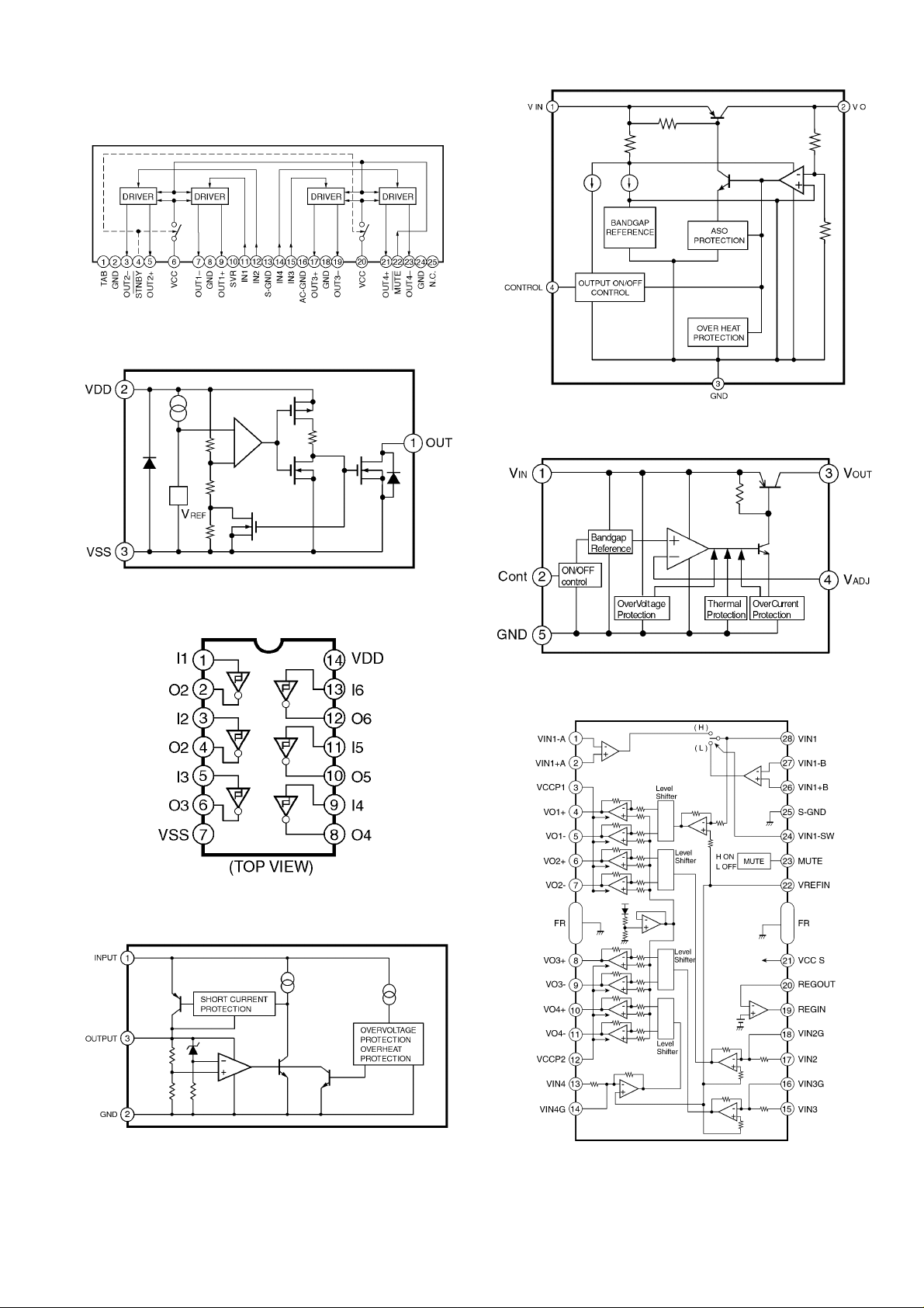
4.2. IC Block Diagram
4.2.1. Main Block
IC271 : YESAM274
IC750 : YESAM267
IC602 : YESAM390
IC650 : YESAM391
IC791 : YESAM344
IC740 : YESAM299
IC802 : YESAM352
7
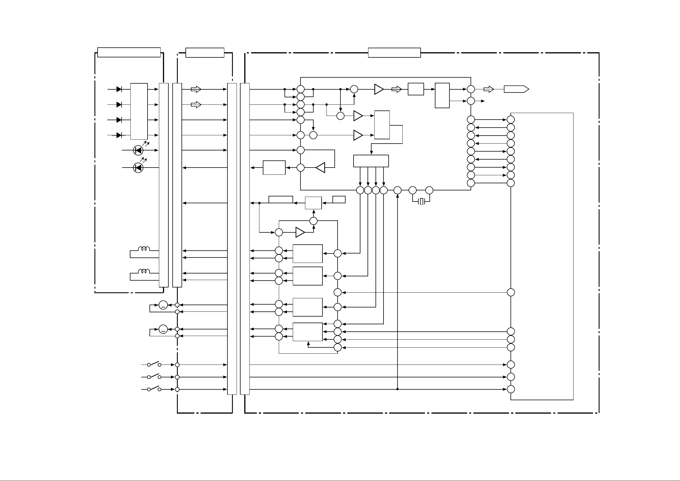
5 Block Diagram
5.1. Main-1 Block
7228-02-11(1/3)
AT51
TU+B
FM / AM TUNER
AM ANT
1
2 FM ANT
FM VT
Q401
Q52,602
Q55,601
PA51
L-CH
R-CH
AM VT
VSM
FM / AM IFC
FM / AM OSC
POW
SW
POW
SW
16
17
22212011146
SD / ST IND
IC681
EEPROM
FM VCC
AM VCC
AUX L
HUB L
R-CH
DO
DI
SK
CS
IC201
AUDIO SIGNAL PROCESSOR
7
5
INPUT
1
3
SEL
SDA
SPECTRUM
ANALIZER
SCLK
CD L
58
54
53
IC601(1/3)
SYSTEM CONTROL
82
ST
16
VSM
92
FM/AM IFC
90
FM/AM OSC
94
EO
6
5
4
3
83
DI / DO
85
SK
84
CS
79
FM MODE
80
AM MODE
AMP MUTE
LOUDNESS
VOLUME
EQALIZER
57
SDA
53
54SCLK
58DATA
57CLK
XT2
10
12CF1
13CF2
99AF MUTE
59STBY
100
70EXT MUTE
XL602
32.8KHz
9XT1
XL601
13.5MHz
SUB
WOOFER
SW
FADER
RL
FL
26242217182930
CQ-C3405U
IC381
LINE AMP
SIGNAL
3
LIFT
R-CH
7
R-CH
IC231
LINE AMP
SIGNAL
3
LIFT
FRONT REAR
CQ-C3305U
CN250
PREOUT
CN251
SUB.W
LR LR LR
R-CH
12
Q364
11
Q261
Q345,346
12
Q251
Q363
MUTE
MUTE
SW
MUTE
R-CH
POWER AMP
12
14
99
IC271
STBY
59
21
23
MUTE
224
100
BATT
ACC
AMP CNT
R-CH
FL+
5
FL-
3
RL+
RL-
R-CH
TEL MUTE
70
CN701
FR+
FR-
RR+
RR-
21
43
65
87
10 9
1211
1413
1615
CQ-C3405U/C3305U MAIN(1/3)
8

5.2. Main-2/Display/Connector Block
7228-02-11(2/3)7221-03-117228-05-11
LD901
KEY-IN
MATRIX
LCD DRIVE
SEG
1–39
3–39
44,45
COM
1–4
KS
3–6
KI
1–5
50–54 46–49 40–43
IC901
RED
2
Q930
LED
DRIVE
DI
DO
CL
CE
64
61
63
62
D901
IC905
IR
RECEIVE
SW901
IC601(2/3)
SYSTEM CONTROL
CN971CN991 CN990CN901
11
11
12
10
5
3
3
5
6
12
2
8
9
LCD5V
OP/CL
RM DATA
ROT1
ROT2
SW990
2
10
1
6
14
13
99
1111
88
1212
1515
66
77
1414
1313
11
Q972
PWR
SW
BATT
MODE A
MODE B
ACC
VDD5V2
LCD5V CNT
Q701,702
BATT
CHECK
SW971
R702,703
ACC
CHECK
49
LCD DI
50
LCD DO
51
LCD CLK
52
LCD CE
66
71
OP/CL
69
BATT
65
PANEL IN
5
RM DATA
73
ROTARY1
72
ROTARY2
68
EJECT
20
ACC
HUB TX
HUB RX
CDC DATA
CDC REMO
CDC CLK
CDC STB
HUB CNT
EVENT
HUB ACC
RESET
AMP CNT
POWER CNT
CNT
75
76
24
74
25
6
46
7
21
22
45
8
98
32
BATT
12
BATT
IC602
RESET
BATT
HUB L
R-CH
IC650
6
3
8
12
11
2
1
Q704,752
IC750
5
4
9
INV
13
10
1
IC791
15V
LIMIT
2
PWR
SW
4
12
REG
3
VDD5V2
L-CH
R-CH
DATA
REMO
SCLK
STRB
HCNT
EVENT
SYS ID1
SYS ID2
ACC
AMP CNT
REG
Q770
TU+B
CN650
3
456
78910
11 12
2131
AUX
CN902
ILL9V
R-CH
Q971
22
4
4
9
13
1010
55
9V
9
LED
DRIVE
AUX L
64
EJ ILL
BATT
CQ-C3405U/C3305U MAIN(2/3)/DISPLAY/CONNECTOR
IC740
13
REG
Q750
PWR
SW
Q740
PWR
SW
9V
SW5V
VDD5V
VDD5V2
5.3. Main-3/CD Interface Block
Optical Pic-Up Ass'y
A
B
E
F
PD
LD
I-V
AMP
3032-14-50
CN2CN2 CN1
A
B
E
F
LPD
LD3.3V
CN801
9
7
3
5
13
21
22
Q871
LD
DRIVE
CD3.3V
IC802
PICK-UP DRIVE
14
13
19
18
7228-02-11(3/3)
IC801
RF AMP,SERVO,DSP
L-CH
DAC
R-CH
DO
DI
CL
CE
CD MUTE
RESB
CD ERROR
SUB READY
REG READY
76
78
46
45
44
43
50
47
51
49
48
R-CH
CD L
IC601(3/3)
SYSTEM CONTROL
27 CD DO
CD DI
26
28 CD CLK
29 CD CE
30 CD MUTE
31 CD RESET
41 CD ERROR
33 SUB READY
REG READY
34
PU IN
EFM
DEM
X IN
72
733224252322
XL801
16.93MHz
X OUT
5
6
7
8
-
Q851
REG
19
9V
+
-
FE
TE
SERVO
CTL
FDO
TDO
ADC
SLDO
SPDO
FOCUS
COIL
TRACKING
COIL
SPINDLE
MOTOR
SLED
MOTOR
20
F+
F-
T+
T-
M
M
CD LIMIT SW
SP+
SP-
SL+
SL-
CD SW1
CD SW2
14
16
18
20
10
19
17
15
8
9
10
11
8
4
6
6
7
4
5
FOCUS
COIL
DRIVE
TRACKING
COIL
DRIVE
SPINDLE
MOTOR
DRIVE
SLED
MOTOR
DRIVE
MUTE
16
14
23
18
26
27
24
37 CD DMUTE
1
43 CD EM
44 CD LM
38 CD S/L
35 CD SW1
36 CD SW2
42 CD LIMIT SW
10
CQ-C3405U/C3305U MAIN(3/3)
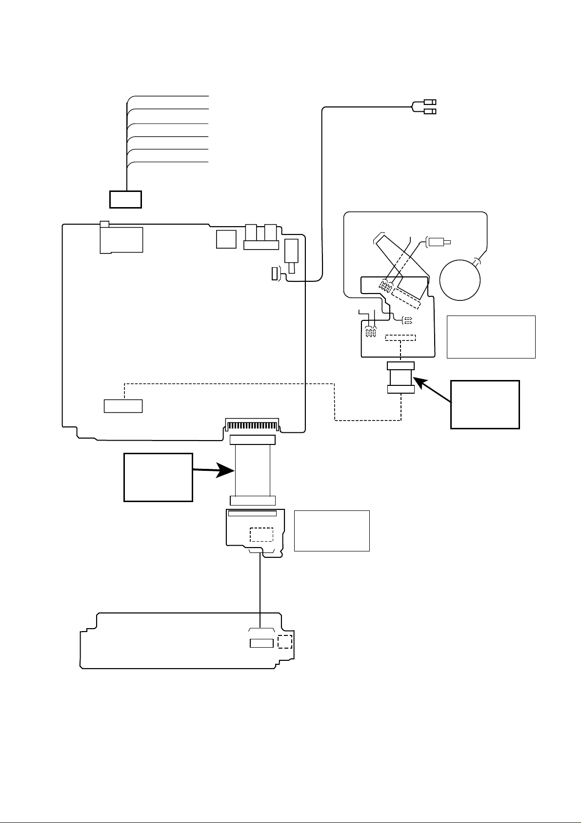
6 Wiring Connection Diagram
4
Power
Connector
/
4
/
2
13 1
CN701
Main P.C.B
[7228-02-11]
Rear Speakers
Front Speakers
External Amplifier Control
Battery(15A)
Ground
Power (ACC or IGN)
Preamp Out
System
(Front) (Rear)
up
10
7
11
12
CN650
31
2
CN250
64
5
4
1
CN251
AT051
Optical
Pic-Up
Ass'y
SW2
SW1
L
<S.W-OUT>
R
Loading/Feed
Limit
SW
1
22
21
Motor
Spindle
Motor
CN2
16
2
1
CN1
CD Interface P.C.B
[3032-14-50]
(Bottom View)
22
21
CN801
Extension
Connector
Jig Part No.
[YESFZS2067]
2
1
Display P.C.B
[7228-05-11]
(Bottom View)
1
1
CN991
CN901
CN971
CN990
1
14
7
8
Extension
Connector
17
Connector P.C.B
17
7
8
1
14
[7221-03-11]
(Bottom View)
CN902
3
12
AUX
Jig Part No.
[YESFZS2076]
11
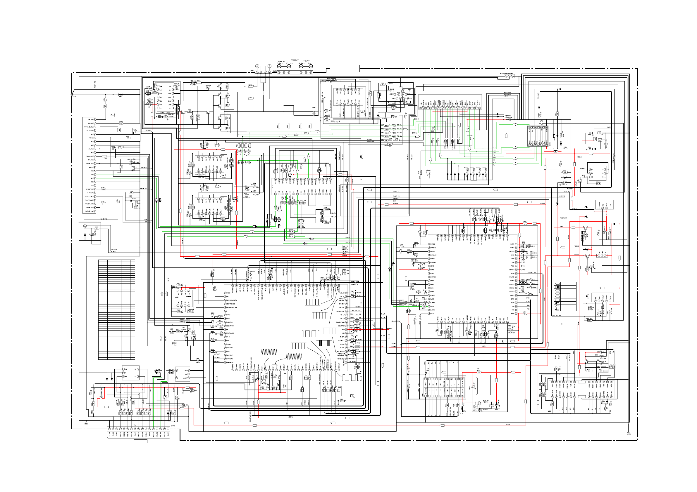
7 Schematic Diagram
7.1. Main Block[CQ-C3405U]
IC231
YESAM338
6.6
1.5
6.6
6.6
6.6
8.8
8.1
9V
R
D251,D351
YESAD174
D351
IC231
L
L
YESAN088
8.5
9.1
D770
YESAD123
PA051
YESAP387
8.4(8.4)
Q770
Q770
9.1
FM(AM)
0(0)
0(0)
Q055
YESAN117
0(0)
8.4
1.3(2.0)
0(0)
0(0)
0(8.3)
0(0)
0(0)
300
8.0(0)
8.4(8.4)
1.3(2.0)
Q052
YESAN117
0(0)
3.6(3.6)
3.6(3.6)
0(0)
0(0)
0.2(0)
5.0(5.0)
0(0)
IC601
CD
AM
FM
1
0
0
0
2
0
0
0
3
0
0
0
4
0
0
0
5
4.8
4.8
4.8
6
0
0
0
7
0
0
0
8
4.8
4.8
4.8
9
1.0
1.0
1.0
10
1.4
1.4
1.4
11
0
0
0
12
1.4
1.4
1.4
13
1.3
1.3
1.3
14
5.0
5.0
5.0
15
5.0
5.0
5.0
16
0.2
0
0.2
17
0
0
0
18
0.3
0
0
19
-
-
-
20
5.0
5.0
5.0
21
4.9
4.9
4.9
22
4.9
4.9
4.9
23
-
-
-
24
0
0
0
25
0
0
0
26
4.8
0
0
27
3.5
5.0
5.0
28
4.7
4.7
4.7
29
1.6
0
0
30
5.0
0.2
0.2
31
4.8
4.8
4.8
32
5.0
5.0
5.0
33
4.7
5.0
5.0
34
0
5.0
5.0
35
0
0
0
36
0
0
0
37
5.0
0
0
38
5.0
5.0
5.0
39
0
0
0
40
5.0
5.0
5.0
41
0
0
0
42
5.0
5.0
5.0
43
0
0
0
44
0
0
0
45
0
0
0
46
5.0
5.0
5.0
47
-
-
-
48
-
-
-
49
4.8
4.8
4.8
50
4.8
4.8
4.8
D976,D978
YESAD133
D978
D976
0
5.0
5.0
Q972
YESAN118
5V
Q061
0
YESAN122
8.4
8.4
0
0
Q062
YESAN122
3.3
Q062
7.8
0
5.0
8.4
0
D053
D053
YESAD119
CD
AM
FM
5.0
5.0
5.0
51
0
0
0
52
5.0
5.0
5.0
53
5.0
5.0
5.0
54
5.0
5.0
5.0
55
0
0
0
56
0
0
0
57
0
0
0
58
5.0
5.0
5.0
59
-
-
-
60
-
-
-
61
-
-
-
62
-
-
-
63
5.0
5.0
5.0
64
0
0
0
65
0
0
0
66
-
-
-
67
5.0
5.0
5.0
68
5.0
5.0
5.0
69
5.0
5.0
5.0
70
4.8
4.8
4.8
71
0
0
0
72
5.0
5.0
5.0
73
0
0
0
74
0
0
0
75
0
0
0
76
-
-
-
77
-
-
-
78
5.0
0
5.0
79
0
5.0
0
80
0
0
0
81
5.0
5.0
5.0
82
0
0
0
83
0
0
0
84
0
0
0
85
0
5.0
5.0
86
3.0
3.0
3.0
87
0
0
0
88
5.0
5.0
5.0
89
0
1.3
1.3
90
0
0
0
91
0
0
0
92
0
0
0
93
0
2.2
2.2
94
0
0
0
95
0
0
0
96
0
0
0
97
4.8
4.8
4.8
98
5.0
5.0
5.0
99
5.0
5.0
5.0
100
D977
YESAD150
9V
7228-02-11
Q346
Q345
YESAN118
YESAN121
YESAN118
6.6
IC381
4.7
6.6
4.7
Q345
0
0
Q261
0
0
6.6
6.6
0
6.6
6.6
6.6
IC281
YESAM338
0
6.6
5V
-0.2
Q263
0
Q364
6.6
6.6
6.6
6.604.7
YESAN121
-0.2
Q363
0
Q264
0
8.8
0
8.8
0
0
0
0
0
0
0
0
0
0
0
0
9V
8.1
4.7
8.1
5V
9V
565656
R
4.7
4.7
100p
0.01
4.7
4.7
4.7
4.7
RL
RR
FL
FR
56
RR
RL
FR
FL
4.4
4.4
4.4
4.4
5.0
5.0
4.4
4.4
IC601
1V / DIV, 0.1µs / DIV
4.4
8.8
8.8
IC201
YESAM384
4.4
4.4
4.3
2V / DIV, 10ms / DIV
4.4
4.3
4.3
L
2V / DIV, 50ms / DIV
2V / DIV, 20ms / DIV
4.4
R
2V / DIV, 10ms / DIV
2V / DIV, 5ms / DIV
4.4
0
4.4
4.4
0.027
2V / DIV, 20µs / DIV
D601
D601
YESAD143
5V
0.027
R
YESAM389
L
L
0.6
4.4
9V
5V5V
2V / DIV, 50ms / DIV
5.004.9
0
4.9
9V
000
4.4
5V5V
0
5.0
IC650
YESAM391
0
5.0
4.3
2V / DIV, 20ms / DIV
5V
0
4.9
YESAD144
5V
5V
5V
D651
YESAD119
D651
RR
D650
5V
5V
R
L
5V
5V
5V
5V
0
7.1
4.6
7.1
RL
FL
FR
100k
3.2
1.3
1.6
1.6
0
1.5
0
3.2
3.3V
0
1.5
1.6
3.2
3.2
1.6
1.6
1.6
0
1.6
3.3V
3.3V
5V
3.3V
0
0
14.8
RL
0.47/50V
D270–D277
YESAD146
1.6
IC271
YESAM274
7.007.1
8.8
3.8
3.803.8
3.8
3.8
7.107.1
10/16V
RR
D270
0
2.2
1.6
1.6
9V9V
14.8
D278,279
YESAD146
0
0
7.1
4.8
7.1
FR
FL
D271
D272
D273
D274
D275
D276
4.7
5.000
000
3.2
IC801
YESAM393
1.7
1.7
1.7
1.7
2.7
1.6
1.602.0
Q871
YESAN113
1.8
0
To CD
3.1
2.5
D277
4.9
2.0
Interface
D278
D279
9V9V
1.5
3.4
4.7
3.5
1.6
2.5
3.2
1.6
3.3V
CN1
3032-14-50
FL
FR
RR
RL
5V5V
3.3V
0
3.2
0
3.2
1.5
0
3.2
0
3.2
0
5.0
3.2
1.1
1.2
1.2
0
1.7
1.6
1.7
1.6
3.2
0
0
3.3V
5V
3.3V3.3V
D704
YESAD143
NCNCNC
CNT
AMP.ANT
5V
5V
3.3V3.3V
5V
3.3V
9V
8V
YESAD146
YESAD139
D701
D703
YESAD119
D795
YESAD144
5V
5V
The following symbols
are shown on the
schematic diagram.
+B
Acc
9V
9V
8V
8V
5V
5V
3.3V
3.3V
RADIO (L,R)
AUDIO (L,R)
CD(L,R)
3.3V
9V
1.5
1.6
1.6
1.6
8.3
3.8
D705
D701
D763
YESAD144
1SS133T77
9V
4.9
4.901.5
3.8
4.1
YESAN129
YESAN126
9V
5V
D741
1.6
3.4
Q702
Q701
Q704
YESAN123
0
4.8
0
YESAM352
D761
YESAD140
YESAD146
D760
Q750
5.0 5.0
D741
5.0
8V8V
Q740,Q750
YESAN079
D791
YESAD146
8.4
3.3
IC802
D760
Q740
5.5
5.6
D791
YESAN148
8.3
5.0
Q702
0
5.0
0
0
Q701
0.9
D702
YESAD153
Q752
YESAN115
14.8
14.8
14.8
14.8
5.1
14.8
IC750
YESAM267
9.105.0
14.4
D750
YESAD141
IC740
YESAM299
5.0
5.0
Q851
7.8
3.6
14.5
0
IC791
YESAM344
000
0
14.8
1.6
1.6
7.7
1.2
8.3
1.6
1.6
4.0
3.9
3.8
Q251
YESAN119
5.0
5.0
5V
5V
5.0
IC681
0
2.2
Q401
IC602
9V
D991
0
0
0
0
0
1.3
0
5V
Q971
YESAN120
0
5.0
4.8
56
Q263,264,363,364
6.6
YESAM338
8.1
6.6
8.1
5V
8.1
4.6
0
6.6
0
4.6
R
YESAM392
Q401
B1CBGF000005
YESAM390
D251
5.0
5.0
Q971
0
D991
YESAD155
To Connector 7221-03-11 CN990
CQ-C3405U MAIN
12
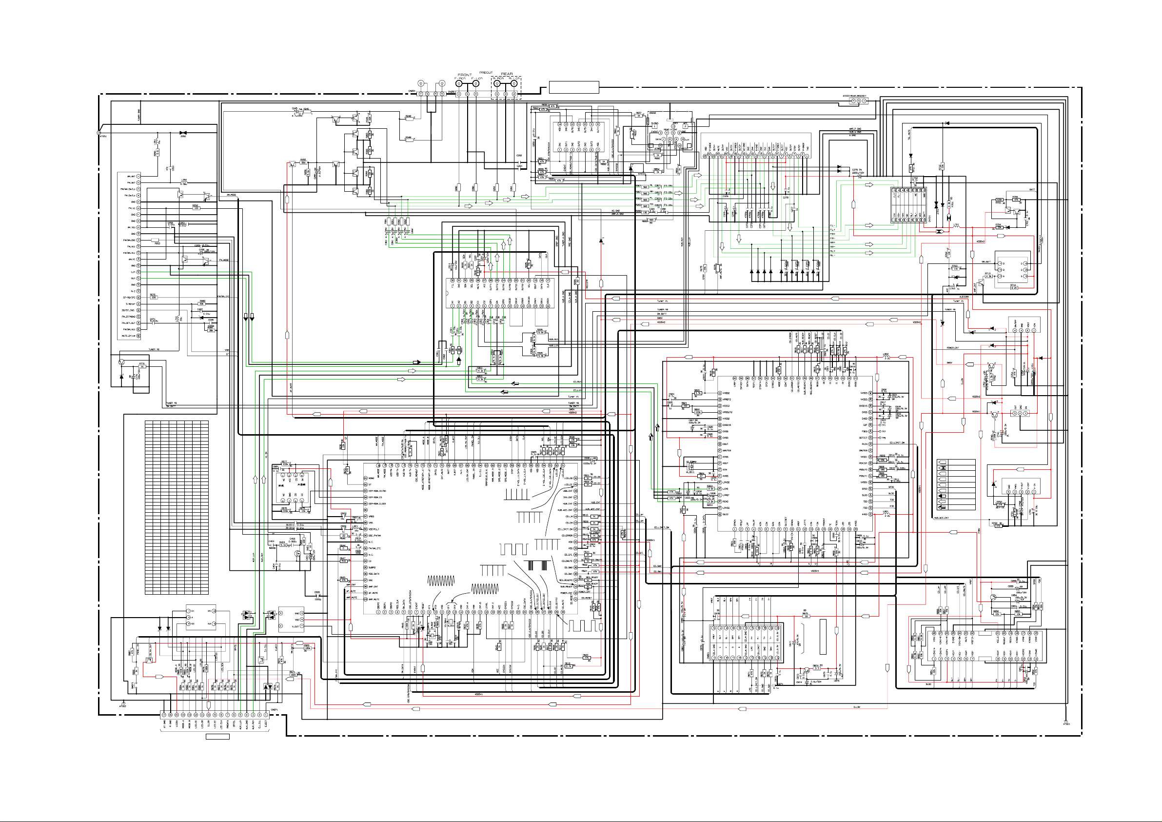
7.2. Main Block[CQ-C3305U]
PA051
YESAP387
FM(AM)
0(0)
YESAN088
8.5
9.1
D770
YESAD123
Q770
8.4(8.4)
Q770
9.1
0(0)
Q055
YESAN117
0(0)
8.4
1.3(2.0)
0(0)
0(0)
0(8.3)
0(0)
0(0)
300
8.0(0)
8.4(8.4)
1.3(2.0)
Q052
YESAN117
0(0)
3.6(3.6)
3.6(3.6)
0(0)
0(0)
0.2(0)
5.0(5.0)
0(0)
IC601
CD
AM
FM
1
0
0
0
2
0
0
0
3
0
0
0
4
0
0
0
5
4.8
4.8
4.8
6
0
0
0
7
0
0
0
8
4.8
4.8
4.8
9
1.0
1.0
1.0
10
1.4
1.4
1.4
11
0
0
0
12
1.4
1.4
1.4
13
1.3
1.3
1.3
14
5.0
5.0
5.0
15
5.0
5.0
5.0
16
0.2
0
0.2
17
0
0
0
18
0.3
0
0
19
-
-
-
20
5.0
5.0
5.0
21
4.9
4.9
4.9
22
4.9
4.9
4.9
23
-
-
-
24
0
0
0
25
0
0
0
26
4.8
0
0
27
3.5
5.0
5.0
28
4.7
4.7
4.7
29
1.6
0
0
30
5.0
0.2
0.2
31
4.8
4.8
4.8
32
5.0
5.0
5.0
33
4.7
5.0
5.0
34
0
5.0
5.0
35
0
0
0
36
0
0
0
37
5.0
0
0
38
5.0
5.0
5.0
39
0
0
0
40
5.0
5.0
5.0
41
0
0
0
42
5.0
5.0
5.0
43
0
0
0
44
0
0
0
45
0
0
0
46
5.0
5.0
5.0
47
-
-
-
48
-
-
-
49
4.8
4.8
4.8
50
4.8
4.8
4.8
D976,D978
YESAD133
D978
D976
0
5.0
5.0
Q972
YESAN118
5V
Q061
0
YESAN122
8.4
8.4
0
0
Q062
YESAN122
3.3
Q062
7.8
0
5.0
8.4
0
D053
D053
YESAD119
CD
AM
FM
5.0
5.0
5.0
51
0
0
0
52
5.0
5.0
5.0
53
5.0
5.0
5.0
54
5.0
5.0
5.0
55
0
0
0
56
0
0
0
57
0
0
0
58
5.0
5.0
5.0
59
-
-
-
60
-
-
-
61
-
-
-
62
-
-
-
63
5.0
5.0
5.0
64
0
0
0
65
0
0
0
66
-
-
-
67
5.0
5.0
5.0
68
5.0
5.0
5.0
69
5.0
5.0
5.0
70
4.8
4.8
4.8
71
0
0
0
72
5.0
5.0
5.0
73
0
0
0
74
0
0
0
75
0
0
0
76
-
-
-
77
-
-
-
78
5.0
0
5.0
79
0
5.0
0
80
0
0
0
81
5.0
5.0
5.0
82
0
0
0
83
0
0
0
84
0
0
0
85
0
5.0
5.0
86
3.0
3.0
3.0
87
0
0
0
88
5.0
5.0
5.0
89
0
1.3
1.3
90
0
0
0
91
0
0
0
92
0
0
0
93
0
2.2
2.2
94
0
0
0
95
0
0
0
96
0
0
0
97
4.8
4.8
4.8
98
5.0
5.0
5.0
99
5.0
5.0
5.0
100
D977
YESAD150
9V
R
D251,D351
YESAD174
D351
L
L
R
D251
5.0
5.0
Q971
0
D991
Q251
YESAN119
5.0
5.0
5V
5V
5.0
IC681
YESAM392
0
Q401
2.2
Q401
B1CBGF000005
IC602
YESAM390
9V
D991
YESAD155
7228-02-11
Q346
0
Q345
YESAN121
YESAN118
0
YESAN121
0
-0.2
-0.2
0
0
0
Q263
0
0
0
Q363
0
Q261
0
0
Q264
0
0
0
0
0
0
Q364
0
5V
5V
18
18
100p
0.01
18
18
18
18
RL
RR
FL
FR
180
180
180
180
RR
RL
FR
FL
4.4
5.0
5.0
4.4
4.4
IC601
1V / DIV, 0.1µs / DIV
4.4
8.8
8.8
YESAM384
4.4
4.4
4.3
2V / DIV, 10ms / DIV
IC201
4.3
4.4
0
4.4
4.4
0.027
2V / DIV, 20µs / DIV
D601
D601
YESAD143
5V
0.027
R
YESAM389
L
L
R
4.4
4.4
4.4
4.4
4.3
L
2V / DIV, 50ms / DIV
2V / DIV, 10ms / DIV
2V / DIV, 20ms / DIV
0.6
4.4
R
2V / DIV, 5ms / DIV
000
4.4
4.4
5V5V
2V / DIV, 50ms / DIV
5V5V
5.004.9
4.9
9V
180
YESAN118
Q263,264,363,364
0
5V 5V
0
0
0
0
1.3
0
0
5.0
4.8
5V
Q971
YESAN120
5.0
IC650
YESAM391
0
0
5.0
2V / DIV, 20ms / DIV
5V
0
0
4.9
YESAD144
5V
5V
5V
D651
YESAD119
D651
RR
D650
5V
R
L
5V
5V
5V
5V
0
7.1
4.6
7.1
RL
FL
FR
100k
3.2
1.3
1.6
1.6
0
1.5
0
3.2
3.3V
3.3V
3.3V
0
1.5
1.6
3.2
3.2
1.6
1.6
1.6
0
1.6
3.3V
5V
0
0
4.3
14.8
RL
0.47/50V
D270–D277
YESAD146
1.6
IC271
YESAM274
14.8
7.007.1
8.8
3.8
3.803.8
3.8
3.8
7.107.1
0
7.1
4.8
7.1
FR
10/16V
FL
RR
D270
D271
D272
D273
D274
D275
D276
4.7
5.000
000
0
3.2
IC801
YESAM393
2.2
1.7
1.6
1.6
1.7
1.7
1.7
2.7
1.6
1.602.0
Q871
YESAN113
1.8
9V9V
D277
0
4.9
2.0
To CD
3.1
2.5
D278
D279
9V9V
3.4
4.7
3.5
1.6
3.2
1.6
3.3V
CN1
Interface
3032-14-50
FL
FR
RR
RL
5V5V
0
1.5
2.5
0
3.3V
3.2
0
3.2
1.5
0
3.2
0
3.2
0
5.0
3.2
1.1
1.2
1.2
0
1.7
1.6
1.7
1.6
3.2
0
3.3V
5V
3.3V3.3V
9V
D278,279
YESAD146
0
D704
YESAD143
NCNCNC
CNT
AMP.ANT
5V
5V
3.3V3.3V
5V
3.3V
8V
YESAD146
YESAD139
D701
D703
YESAD119
D795
YESAD144
5V
5V
The following symbols
are shown on the
schematic diagram.
+B
Acc
9V
9V
8V
8V
5V
5V
3.3V
3.3V
RADIO (L,R)
AUDIO (L,R)
CD(L,R)
3.3V
9V
1.5
1.6
1.6
1.6
8.3
3.8
D705
D701
YESAD144
D763
4.901.5
3.8
YESAN129
YESAN126
9V
5V
D741
1SS133T77
9V
1.6
4.9
4.1
3.4
Q702
Q701
Q704
YESAN123
0
4.8
0
YESAM352
D761
YESAD140
YESAD146
D760
Q750
5.0 5.0
D741
5.0
5.5
8V8V
Q740,Q750
YESAN079
D791
YESAD146
8.4
3.3
IC802
D760
5.6
Q740
D791
5.0
5.0
Q701
14.8
14.8
5.1
5.0
Q851
YESAN148
7.8
1.2
8.3
3.6
YESAD153
Q752
YESAN115
5.0
7.7
4.0
3.9
Q702
0
0
0.9
D702
14.8
14.8
14.8
YESAM267
IC740
YESAM299
1.6
3.8
0
IC750
0
000
8.3
9.105.0
14.5
IC791
YESAM344
0
14.8
1.6
1.6
14.4
D750
YESAD141
1.6
To Connector 7221-03-11 CN990
CQ-C3305U MAIN
13
 Loading...