

ORDER NO. ACED070207C8
AUTOMOTIVE AFTERMARKET
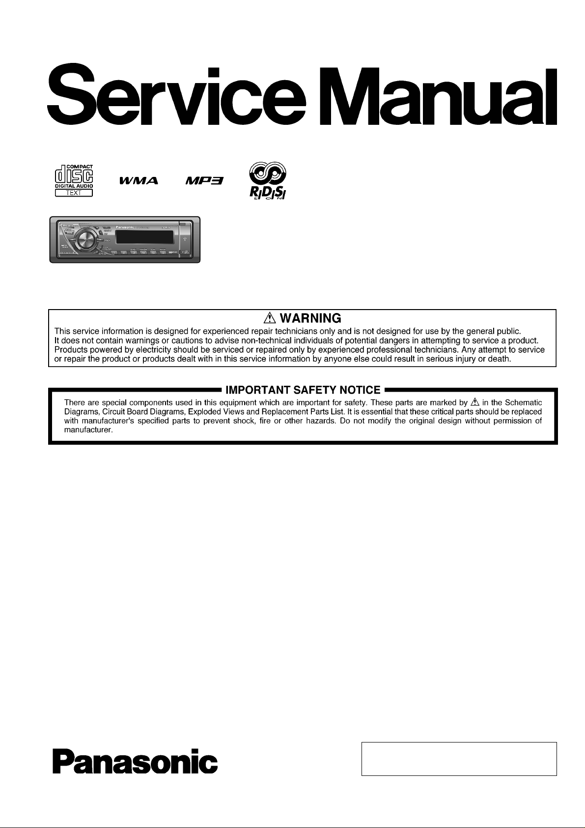
CQ-C3355N
WMA MP3 CD Player/Receiver
TABLE OF CONTENTS
PAGE P AGE
1 Service Navigation ----------------------------------------------- 2
2 Specifications ----------------------------------------------------- 3
3 Features ------------------------------------------------------------- 4
4 T ec hnic al Desc ri ptions----------------------------------------- 5
5 Block Diagram----------------------------------------------------- 8
6 Wiring Connection Diagram---------------------------------11
7 Schematic Diagram---------------------------------------------12
8 Schematic Diagram-2------------------------------------------15
9 Printed Circuit Board-------------------------------------------17
10 Exploded View and Replacement Parts List -----------22
11 Schematic Diagram for Printing with A4 Size----------32
© 2007 Matsushita Electric Industrial Co., Ltd. All
rights reserved. Unauthorized copying and distribution is a violation of law.
1 Service Navigation
1.1. About Lead Free Solder (PbF)
Distinction of PbF PCB :
• PCBs (manufactured) using lead free solder will have a Pb F
stamp on the PCB.
Caution :
• Pb free solder has a higher melting point than standard solder; Typically the melting point is 50 - 70°F (30 - 40°C)
higher. Please use a soldering iron with temperature control
and adjust it to 700 ± 20°F (370 ± 10°C). In case of using
high temperature soldering iron, please be careful not to
heat too long.
• Pb free solder will tend to splash when heated too high
(about 1100°F/600°C)
• This lead free solder will be used for the products after serial
No. 1,000,001.
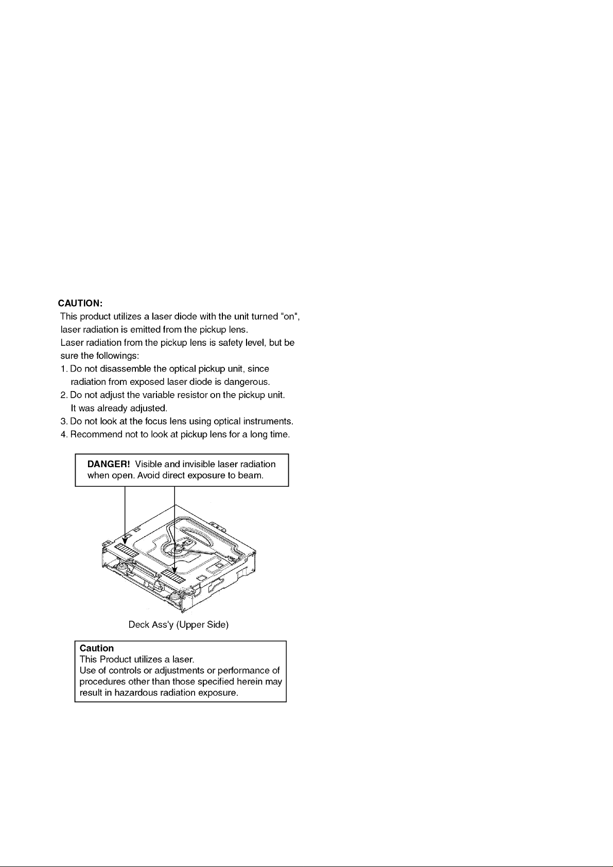
1.2. Laser Products
1.4. Maintenance
Your product is designed and manufactured to ensure a minimum of maintenance. Use a dry, a soft cloth for routine exterior
cleaning. Never use benzine, thinner or other solvents.
1.5. Notes
[RADIO BLOCK]
Do not align the AM/FM package block. When the package
block is necessary, it will be supplied alrea dy alig ned at the factory.
[CD DECK BLOCK]
This model has no servo alignment points because microcomputer controls the servo circuit.
1.3. Replacing the Fuse
Use fuses of the same s pe cif ied rati ng 15 a mps. Using different
substitutes or fuses with higher ratings, or connecting the unit
directly without a fu se, could cause fire or damage to th e st ere o
unit.
2
2 Specifications
2.1. Specifications*
General
Power Supply DC 12V (11V - 16V)
Current Consumption Less than 2.1A (CD mode, 0.5W 4-
Maximum Power Output 50W × 4 (at 1kHz), volume control maxi-
Power Output 22 W x 4 (DIN 45 324, at 4 Ω)
Tone Adjustable Range Bass:±12dB (at 100 Hz),
Speaker Impedance 4 - 8 Ω
Pre-amp Output Voltage 2.5 V (CD mode: 1 kHz, 0 dB)
Pre-amp Output Impedance
USB Connector
USB Standard Compatibility
File System
Maximum Supply Current
Playable Audio Format
Recommended Capacity
AUX input
input impedance
Allowable External
Input
Test Voltage 14.4V
Negative Ground
Speaker)
mum
Treble: ±12 dB (at 10kHz)
200 Ω
1.1/2.0 Full Speed
FAT 12/16/32
500 mA
MP3/WMA
Less than 4 GB (1 partition)
10 kΩ
2.0 V
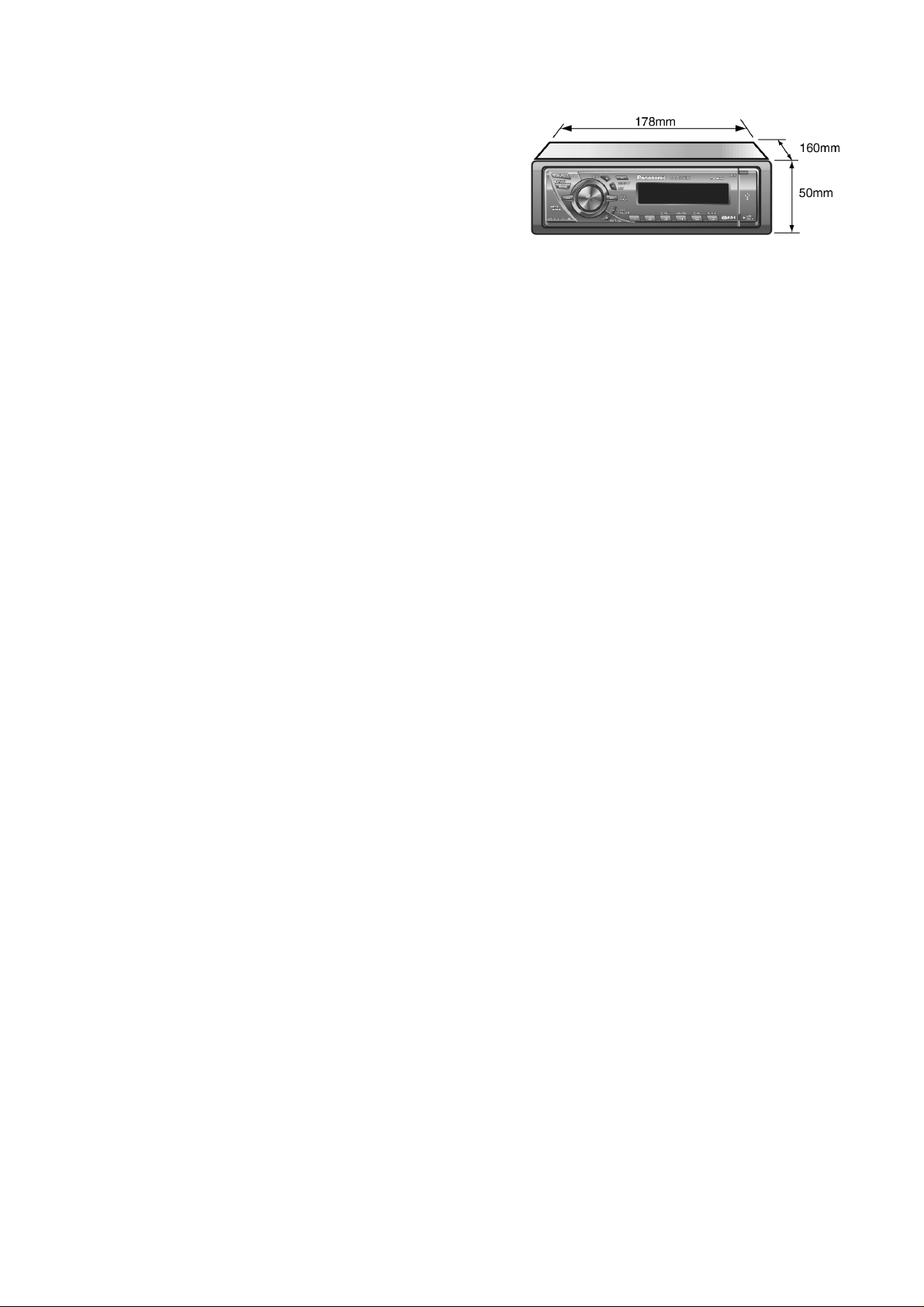
2.2. Dimensions
Dimensions (W×H×D)** 178×50×160mm
Weight** 1.3 kg
CD Player
Sampling Frequency 8 times oversampling
DA Converter 1 bit DAC System
Pick-Up Type Astigma 3-beam
Light Source Semiconductor Laser
Wave Length 790 nm
Frequency Response 20 Hz - 20 kHz (±1 dB)
Signal to Noise Ratio 96 dB
Total Harmonic Distortion
Wow and Flutter Below Measurable Limits
Channel Separation 75 dB
FM Stereo Radio
Frequency Range 87.5 MHz - 108.0 MHz
Usable Sensitivity 6 dB/µV (S/N 30 dB)
Stereo Separation 35 dB (at 1 kHz)
AM (MW) Radio
Frequency Range 531 kHz - 1602 kHz
Usable Sensitivity 27 dB/µV (S/N 20 dB)
AM (LW) Radio
Frequency Range 153 kHz - 279 kHz
Usable Sensitivity 32 dB/µV (S/N 20 dB)
0.01 % (1 kHz)
* Specifications and the design are subject to possible modification
without notice due to improvements.
** Dimensions and Weight shown are approximate.
** Above specifications comply with EIA standards.
3

3 Features
• Hands Free Phone System. (The optional Bluetooth handsfree kit: CY-BT100N)
• Expansion Module (The optional Hub unit: CY-EM100N).
• The optional adapter allows you to connect the optional
Panasonic CD changer unit (CX-DP880 N ).
• The optional adapter allows you to connect the optional
iPod® series.
• SQ (Sound Quality).
• USB Connector.
• MP3/WMA Playback from CD-R/RW.
• Anti-Theft System.
4
4 Technical Descriptions
4.1. Terminals Description
4.1.1. Main Block
IC601 : YESAM402
Pin
No
1 DBGP0 Not used - 0
2 DBGP1 Not used - 0
3 DBGP2 Not used - 0
4 RDS CLK RDS (Radio Data System) clock I 2.4
5 RM DATA Remote control data I 4.7
6 CDC STB/
7 EVENT Hub event detection I 0
8 RESET System reset I 4.8
9 XT1 Crystal oscillator 1 (32.768kHz) I 1.0
10 XT2 Crystal oscillator 2 (32.768kHz) O 1.4
11 VSS Ground - 0
12 CF1 Ceramic oscillator 1 (13.5MHz) I 1.4
13 CF2 Ceramic oscillator 2 (13.5MHz) O 1.3
14 VDD +5V power supply - 4.8
15 INT A Pulled down - 0
16 VSM Signal meter intensity (Tuner) I 0
17 USB FLG USB power switch I 4.8
18 LEVEL Not connected - 19 USB RESET USB reset O 3.3
20 ACC ACC level detection I 4.9
21 SYSID1 Hub connection device identifica-
22 SYSID2 Hub connection device identifica-
23 USB MUTE USB mute O 0
24 CDC DATA Serial data from CD changer I 0
25 CDC CLK/
26 CD DI (CD SI) Serial data to CD and USB O 0
27 CD DO (CD SO) Serial data from CD and USB I 3.3
28 CD CLK Serial clock for CD and USB O 0
29 CD CE (FS) Chip enable for CD and USB O 0
30 CD MUTE CD mute I 0.2
31 CD RESET CD reset O 4.8
32 POWER CNT System power supply control O 4.8
33 SUB READY Sub ready from CD servo I 4.8
34 REG READY Reg. ready from CD servo I 4.8
35 CD SW1 CD detection switch 1 I 0.1
36 CD SW2 CD detection switch 2 I 0.1
37 CD DMUTE Mute for Pick-up driver O 0
38 CD S/L Sleding/Loading mode switch O 4.8
39 VSS Ground - 0
40 VDD +5V power supply - 4.9
41 CD ERROR CD error status I 0.1
42 CD LIMIT SW CD limit detection switch I 4.8
43 CD EM Ejecting mode for Sled motor O 0
44 CD LM Loading mode for Sled motor O 0
45 HUB ACC CNT Power supply control for Hub
46 HUB CNT Hub connection check request O 4.8
47 INV CNT Not connected - 48 USB SLP USB sleep O 0
49 LCD DI Serial data to LCD O 4.7
50 LCD DO Serial data from LCD I 4.8
51 LCD CLK Serial clock for LCD O 4.8
52 LCD CE Chip enable for LCD CPU O 0
53 E-VOL I2C
Port Description I/O Vol
SYSID4
SYSID3
DATA
CD changer Strobe; or Hub connection device identification 4
tion 1
tion 2
Serial clock for CD changer; or Hub
connection device identification 3
(External device)
Serial data for Audio signal processor (volume)
I0
I4.8
I4.8
I0
O0
O4.8
[V]
Pin
No
54 E-VOL I2C CLK Serial clock for Audio signal pro-
55 VDD +5V power supply - 4.8
56 VSS Ground - 0
57 E-VOL LV CLK Serial clock to Audio signal proces-
58 E-VOL LV DATA Serial data from Audio signal pro-
59 STBY Standby mode for Power amplifier O 4.8
60 SRS MODE 1 Not connected - 61 SRS MODE 2 Not connected - 62 SRS MODE 3 Not connected - 63 SRS FOCUS
64 EJ ILL Ejection key illumination control O 4.8
65 PANEL IN Front panel detection I 0.1
66 LCD 5V CNT +5V power supply control for LCD
67 USB IN USB-in detection I 0
68 EJECT Ejection switch I 4.8
69 BATT Battery level detection I 4.9
70 EXT MUTE Telephone mute I 4.8
71 OP/CL Open/Close detection for Front
72 MODE B
73 MODE A
74 CDC REM OUT Remote control for CD changer O 75 HUB-TX Transmission data to Hub O 76 HUB-RX Reception data from Hub I 0
77 UTX2 Serial data to USB O 0
78 URX2 Serial data from USB I 0
79 FM MODE Power supply control for FM mode O 4.8
80 USB ENBL USB enable O 4.8
81 MONO Monaural control O 0
82 ST FM stereo indication I 4.9
83 EEP-ROM DI/DO Not connected - 84 EEP-ROM CS Not connected - 85 EEP-ROM SK Not connected - 86 ANT CNT Not connected - 87 VREG Connected to capacitor - 3.0
88 VSS Ground - 0
89 VDD (PLL) +5V power supply - 4.8
90 OSC FM/AM FM/AM local oscillation frequency I 1.4
91 N.C. Ground - 0
92 FM/AM IFC FM/AM center frequency input I 0
93 N.C. Ground - 0
94 EO FM/AM phase detection error out-
95 SUBPD Not connected - 96 RDS DATA RDS (Radio Data System) data I 2.8
97 SSC SD sensitivity control O 0
98 AMP CNT Power supply control for External
99 AF MUTE Audio signal mute O 4.8
100 AMP MUTE Mute for Power amplifier O 4.8
Port Description I/O Vol
cessor
sor (Audio level)
cessor (Audio level)
ELVL
(ROTARY 2)
(ROTARY 1)
Not connected - -
circuit
panel
Rotary encoder detection B for volume
Rotary encoder detection A for volume
put
amplifier
[V]
O4.8
O0
I0
O0
I4.8
I4.8
I4.8
O2.3
O4.7
5
4.2. IC Block Diagram
4.2.1. Main Block
IC201 : YESAM384
IC602 : YESAM390
IC271 : C1EA00000041
IC501 : YESAM283
IC650 : YESAM391
IC740 : YESAM269
IC750 : YESAM267
6
IC791 : YESAM344
IC802 : YESAM352
PA051 : YESAP413
7
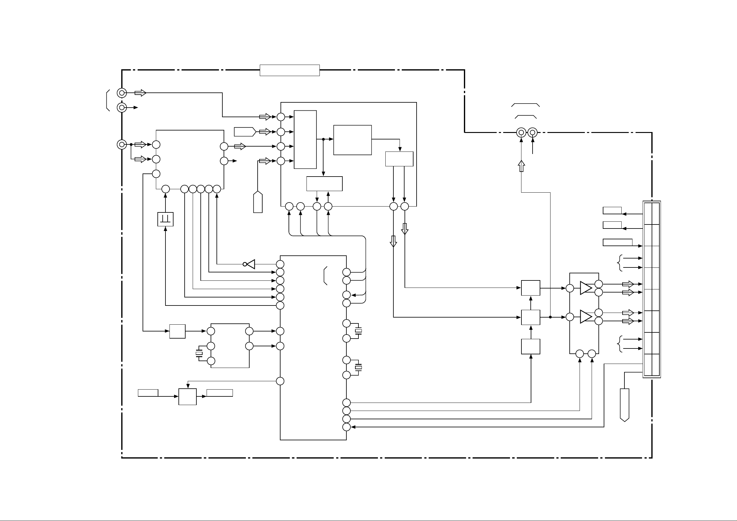
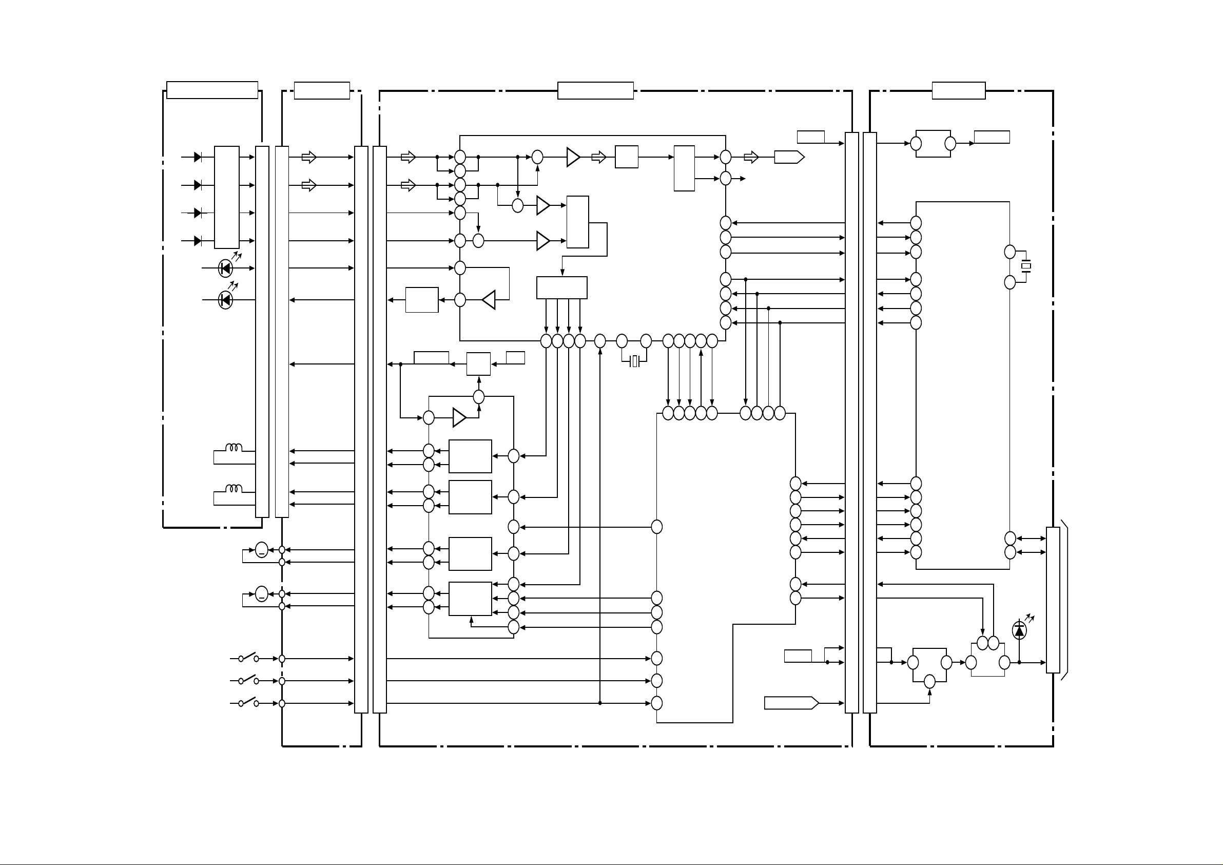
5 Block Diagram
C
5.1. Main-1 Block
7230-02-11(1/3)
58
IC201
LOUDNESS
VOLUME
EQUALIZER
57
DATA
53
54CLK
58DATA
57CLK
XT2
10
12CF1
13CF2
99AF MUTE
59STBY
100
70EXT MUTE
CN250
PREOUT
REAR
LR
FADER
R-CH
RL
FL
262417182930
IC271
POWER AMP
Q363
MUTE
Q364
9XT1
XL602
32.8KHz
XL601
13.5MHz
MUTE
Q251
Q261
MUTE
CONT
12
14
STBY
21
23
MUTE
224
BATT
ACC
AMP CNT
R-CH
FL+
5
FL-
3
RL+
RL-
R-CH
TEL MUTE
CN701
FR+
FR-
RR+
RR-
REMO IN
21
43
65
87
10 9
1211
1413
1615
R
AT051
L
R-CH
7
5
1
3
81
82
16
92
90
94
83
85
79
1
2 FM ANT
19
FM DET
Q401
TU+B
PA051
FM / AM TUNER
AM ANT
VT
FM / AM OSC
Q066
AMP
XL501
4.332MHz
Q055,602
POW
SW
12
L-CH
13
R-CH
17 18161596
VSM
SD / ST IND
FM / AM IFC
RDS DEM
MPX
OSC IN
14
OSC OUT
FM VCC
HUB L
R-CH
CD L
Q054
IC501
24
1613
AUDIO SIGNAL PROCESSOR
INPUT
SEL
SPECTRUM
ANALIZER
SDA
SCLK
54
53
IC601(1/3)
SYSTEM CONTROL
MONO
ST
VSM
FM/AM IFC
OSC FM/AM
EO
RDS DATA
RDS CLK
FM MODE
EVOL
AMP MUTE
N251
AUX
CQ-C3355N MAIN(1/3)
8
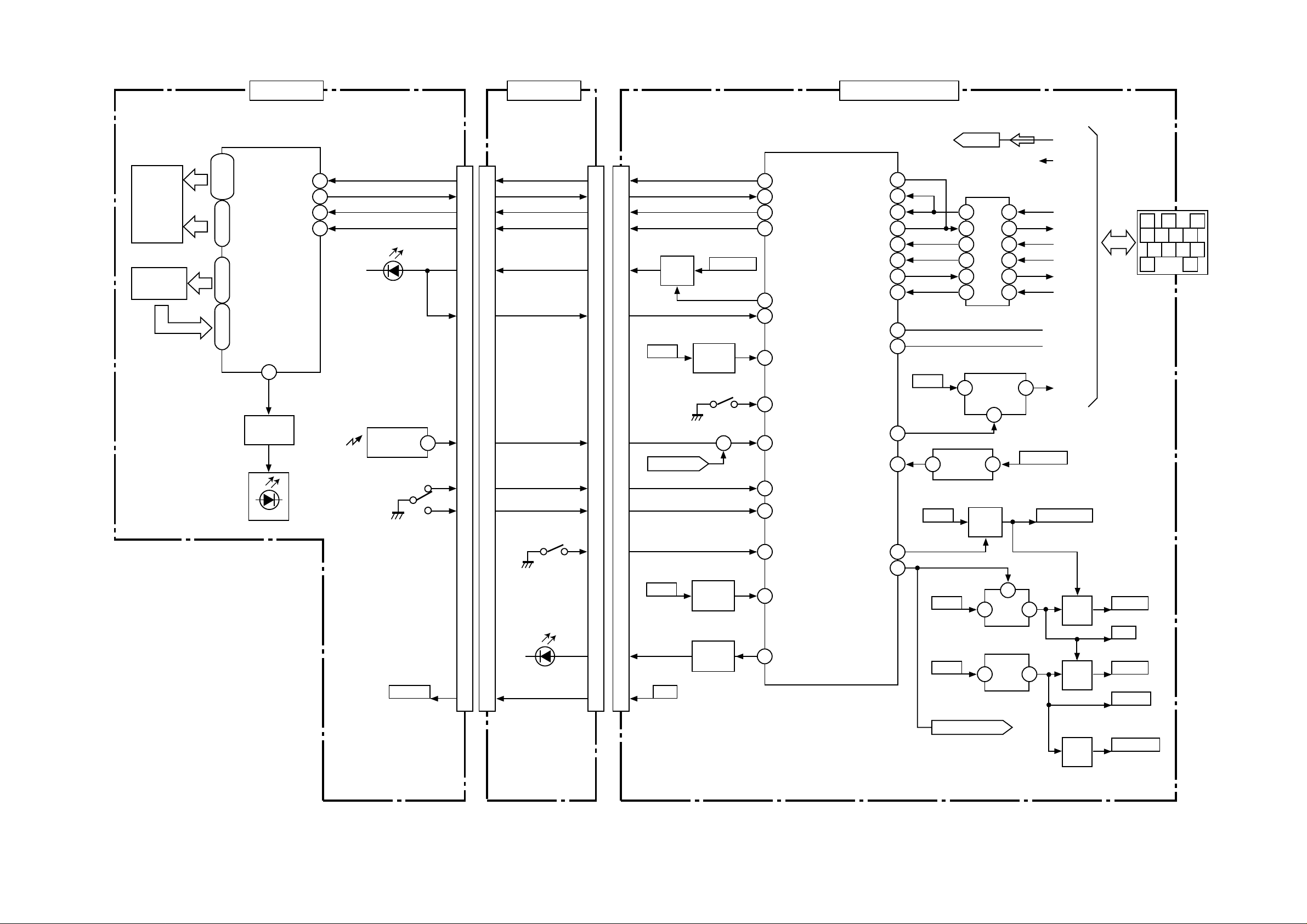
5.2. Main-2/Display/Connector Block
0
7230-02-11(2/3)7230-03-117230-05-12
LD901
KEY-IN
MATRIX
LCD DRIVE
SEG
1–39
3–39
44,45
COM
1–4
KS
3–6
KI
1–5
50–54 46–49 40–43
IC901
RED
2
Q930
LED
DRIVE
DI
DO
CL
CE
64
61
63
62
D901
IC905
IR
RECEIVE
SW901
IC601(2/3)
SYSTEM CONTROL
CN971CN991 CN990CN901
11
11
12
10
5
3
3
5
6
12
2
8
9
LCD5V
OP/CL
RM DATA
ROT1
ROT2
SW990
2
10
1
6
14
13
66
88
55
99
1212
33
44
1111
1010
11
Q972
PWR
SW
BATT
REMO IN
MODE A
MODE B
ACC
VDD5V
LCD5V CNT
Q701,702
BATT
CHECK
SW971
+
R702,703
ACC
CHECK
49
LCD DI
50
LCD DO
51
LCD CLK
52
LCD CE
66
71
OP/CL
69
BATT
65
PANEL IN
5
RM DATA
73
ROTARY1
72
ROTARY2
68
EJECT
20
ACC
HUB TX
HUB RX
CDC DATA
CDC REMO
CDC CLK
CDC STB
HUB CNT
EVENT
HUB ACC
RESET
AMP CNT
POWER CNT
CNT
75
76
24
74
25
6
46
7
21
22
45
8
98
32
BATT
12
BATT
IC602
RESET
BATT
HUB L
R-CH
IC650
6
3
8
12
11
2
1
Q704,752
IC750
5
4
9
INV
13
10
1
IC791
15V
LIMIT
2
PWR
SW
4
12
REG
3
VDD5V2
L-CH
R-CH
DATA
REMO
SCLK
STRB
HCNT
EVENT
SYS ID1
SYS ID2
ACC
AMP CNT
REG
Q770
TU+B
CN65
3
456
78910
11 12
2131
ILL9V
Q971
22
4
4
77
9V
9
LED
DRIVE
64
EJ ILL
BATT
POWER CNT
CQ-C3355N MAIN(2/3)/DISPLAY/CONNECTOR
IC740
13
REG
Q750
PWR
SW
Q740
PWR
SW
9V
SW5V
VDD5V
VDD5V2
5.3. Main-3/CD Interface Block
B
Optical Pick-Up Ass'y
A
B
E
F
PD
LD
I-V
AMP
3032-14-50
CN2CN2 CN1
AA
B
E
F
LPD
LD3.3V
CN801
9
7
3
5
13
21
22
5
6
7
8
14
13
19
Q871
LD
DRIVE
CD3.3V
PICK-UP DRIVE
20
18
IC802
C
B
D
F
-
LDS
LDO
Q851
REG
19
9V
RF AMP,SERVO,DSP
+
-
FE
TE
SERVO
FDO
7230-02-11(3/3)
IC801
EFM
DEM
ADC
CTL
PU IN
733224252322
TDO
SLDO
SPDO
16.93MHz
X IN
XL801
X OUT
72
48
34
DAC
49
33
51
41
L-CH
R-CH
DO
DI
CL
DO
DI
CL
CE
50
47
30
31
76
78
46
45
44
46
45
44
43
R-CH
31
41
7230-06-11
CN885
SW 5V USB 3.3V
CD L
IC601(3/3)
SYSTEM
CONTROL
33
34
8
22
24
21
19
20
18
17
CN101
8
22
24
21
19
20
18
17
IC104
54
REG
USB CONTROL
31
ST DATA
33
ST CK
46
ST REQ
10
CD DATA
9
CD CMD
11
CD CLK
15
CE CD DSP
IC101
CF1
CF2
XL101
6
7
FOCUS
COIL
TRACKING
COIL
SPINDLE
MOTOR
SLED
MOTOR
F+
F-
T+
T-
M
M
CD LIMIT SW
SP+
SP-
SL+
SL-
CD SW1
CD SW2
14
16
18
20
10
19
17
15
8
9
10
11
8
4
6
6
7
4
5
FOCUS
COIL
DRIVE
TRACKING
COIL
DRIVE
MUTE
SPINDLE
MOTOR
DRIVE
SLED
MOTOR
DRIVE
16
14
23
18
1
26
27
24
CD MUTE
CD RESET
CD ERROR
SUB READY
REG READY
37 CD DMUTE
CD EM
43 80
44 CD LM
38 CD S/L
35 CD SW1
36 CD SW2
42 CD LIMIT SW
CD DI
CD DO
CD CLK
POWER CNT
CD CE
78
77
19
23
67
48
17
BATT
USB TXD
USB RXD
14
16
11
15
12
13
3
7
3
4
5
14
16
11
15
12
13
3
7
3
4
5
45
TXD
44
RXD
2
RESET
USB MUTE REQ
16
USB IN
48
47
SLEEP 37
IC103
3
SW
REG
2
4
4
POW
IC102
UHD+
UHD-
31
SW
CN102
D+
38
5
D-
VDD
3
2
US
1
10
CQ-C3355N MAIN(3/3)
6 Wiring Connection Diagram
External Mute
External Remote Control
Power (ACC or IGN)
Ground
Motor Antenna Relay Control
Battery(15A)
L
R
<AUX-Input>
Power
Connector
CN701
Main P.C.B
[7230-02-11]
222
21
1
CN801
Extension
Connector
Jig Part No.
[YESFZS2077]
Speaker
Not Used
System
up
10
12
CN650
1
11
CN971
7
RL-
31
CN250
14
FL-
FR-
RR-
2
64
CN885
ACC
Motor
ANT
4
1
RL+
FL+
FR+
RR+
Preamp Out
(Rear)
GND
BATT
5
CN251
2
1
23
24
AT051
Optical
Pic-Up
Ass'y
SW2
SW1
1
22
21
Limit
SW
16
2
1
Loading/Feed
Motor
CN2
CN1
Spindle
Motor
CD Interface P.C.B
[3032-14-50]
(Bottom View)
Extension
Connector
Jig Part No.
2
1
CN101
23
24
[YESFZS2076]
USB P.C.B
CN102
1
4
[7230-06-11]
(Bottom View)
1
CN990
CN991
1
14
7
8
CN901
14
Connector P.C.B
7
8
1
14
[7230-03-11]
(Bottom View)
Display P.C.B
[7230-05-12]
(Bottom View)
11
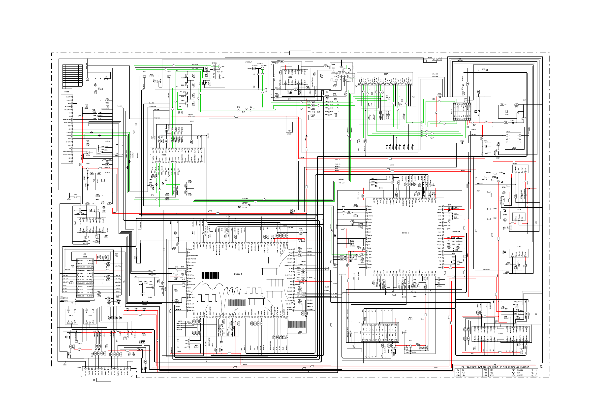
7 Schematic Diagram
7.1. Main Block
7230-02-11
FM
0
1
0
2
0
3
4
5
1.2
6
7.8
7
7.8
8
0
9
0
10
0
11
YESAP413
AM
-
-
1.3
7.8
0.5
YESAD150
0
0
0
-
-
0
0
0
12
13
14
15
16
17
18
19
20
21
4.8
YEAS08042
AM
FM
3.5
3.5
3.5
3.5
0
0
0
0
0
0
4.8
4.9
0
0
0
0
-
-
-
-
7.8
7.9
YESAN117
8V
7.9
(C)
5V
7230-06-11
0
4.9
YESAN118
0
0
YESAN122
YESAN087
8.5
YESAD143
0
0
YESAD150
0
L
0
9.1
YESAD156
4.8
CN101
YESAN132
2.3
2.2
5V
R
L
YESAN119
4.7
0
4.6
YESAN122
0
0
4.8
L
R
R
YESAD119
L
9V
R
L
1.9
1.3
4.7
2.3
2.9
YESAM283
YESAN118
0
0
0
L
0
4.8
8.6
4.8
8.7
4.3
4.3
4.3
R
L
R
4.3
YESAM384
4.3
4.3
4.3
4.2
4.3
R
L
R
L
R
4.3
4.2
YESAN121
YESAN121
YESAN121
YESAN121
L
R
4.3
4.2
0
0
0
0
0
0
0
0
0
0
0
0
4.3
0.6
1/4W
YESAD155
R
L
L
L
9V
0
0
9V
5V
R
R
R
R
L
R
L
2.5
2.4
5V
YESAD133
YESAD133
YESAD155
YESAD133
5V
YESAD133
4.6
YESAN120
YESAD183
0
YESAD183 YESAD183
4.5
9V
YESAD133
5V
2.3
B1CBGF000005
YESAD149
2V/DIV,20ms/DIV
YESAM402
1.3
0
5V
0
4.8
4.8
YESAM390
0.5V/DIV,10us/DIV
2V/DIV,0.2ms/DIV
1V/DIV,10us/DIV
YESAD143
5V
2V/DIV,20ms/DIV
0.2V/DIV,10us/DIV
2V/DIV,50ms/DIV
2V/DIV,20ms/DIV
2V/DIV,20ms/DIV
2V/DIV,0.5ms/DIV
2V/DIV,20ms/DIV
0
0
4.8
YESAM391
4.8
0.4
2V/DIV,0.5s/DIV
0
4.8
0
4.2
0
YESAD119
L
L
R
R
YESAD144
5V
5V
5V
L
R
L
0
6.2
4.5
L
R
L
3.3
3.3
3.2
3.3
0
1.5
3.3V
0
0
0
5V
5V
R
3.3V
3032-14-50
CN1
0
1.6
C1EA00000041
0
0
0
0
6.2
3.3
6.2
3.3
6.2
6.2
13.3
L
16V10
3.3
8.0
3.3
3.3
R
L
R
16V47
YESAD146
YESAD146
YESAD146
9V
9V
5V
5V
YESAD181
YESAD181
YESAD181
3.3V
0
0
0
0
3.3
3.3
3.3
3.1
1.6
1.6
1.6
1.9
1.6
1.9
1.6
1.9
1.6
1.6
3.3V
0
6.2
6.2
4.8
6.3
13.3
L
R
L
R
YESAD146
YESAD146
YESAD146
YESAD146
YESAD146
4.8
0
4.8
0
0
3.3
4.8
YESAM393
0.4
0
1.6
1.6
2.6
1.6
1.6
5V
1/4W
YESAN113
3.2
0.1
1/4W
3.2
L
L
R
R
R
R
L
L
1/4W
0
0
0
0
3.3
3.2
3.3
0
3.3
1.5
0
3.3
3.3
0
0
4.8
3.3
3.2
0
2.5
0
1.7
1.7
1.8
1.8
3.2
3.2
1.6
0.3
3.3V
3.3V
3.3V
0
0
5V
YESAD143
YESAD167
YESAD144
3.3V
3.3V
3.3V
9V
1/4W
4.8
4.8
0
4.8
5V
YESAD146
YESAN129
YESAD139
YESAD119
5V
5V
8V
1.3
0
0.9
1.0
4.8
1.3
1.2
1.3
1.6
8.4
1/4W
4.9
4.9
YESAN126
0
4.7
0
YESAN123
9V
YESAD140
YESAD167
9V
YESAD146
YESAN079
4.9
5V
5.5
5V
YEAD1SS133T
YESAN079
4.8
5V
5.4
9V
8V
3.3V
8.4
3.3
YESAN148
0
1.6
YESAM352
1.3
1.3
8V
4.9
4.9
7.8
8.4
1.3
0
YESAD153
13.3
13.3
4.5
9V
5V
YESAD146
1.2
1.3
5V
0
0
YESAN115
13.3
13.3
13.3
4.8
YESAM269
4.9
YESAM344
0
1.7
7.8
1.3
0
0.8
YESAM267
0
9.1
13.0
YESAD141
0
13.0
0
0
13.3
1.7
1.7
1.7
1.7
1.7
8.4
1.3
7230-03-11
CN990
YESAD165
5V
5V
9V
CQ-C3355N MAIN
12

7.2. Display Block
7230-05-12
1.1
0
YESAD166
YESAD165
YESAD165
YESAD165
0.7
YESAN146
YESAD165
YESAD165
YESAD165
YESAD133
YESAD143
YESAD165
YESAD165
7230-03-11
CN991
To
YESAD165
YESAD165YESAD165
YESAD165YESAD165
YESAD165
K0H1BA000445
YESAM264
YESAS123
4.804.8
9V
5V
5V
9V
K0H1BA000445
K0H1BA000445
K0H1BA000445
K0H1BA000445
K0H1BA000445
K0H1BA000445
K0H1BA000445 K0H1BA000445
K0H1BA000445 K0H1BA000445 K0H1BA000445
K0H1BA000445
K0H1BA000445
K0H1BA000445
YESAD147
YESAD150
9V
5V
2.4
2.4
4.8
4.8
2.4
2.4
2V / DIV, 2ms / DIV
1V / DIV, 2ms / DIV
2.4
2.4
2.4
C0HBA0000195
4.8
4.8
0
0
0
0
0
2V / DIV, 10µs / DIV
0
5V
4.8
3.1
1.6
0
3.8
4.8
0
5.0
4.8
2V / DIV, 5ms / DIV
4.7
2.4
2.4
2.4
2.4
2V / DIV, 2ms / DIV
2.4
2.4
2.4
2.4
2.4
2.4
1V / DIV, 2ms / DIV
2.4
2.4
2V / DIV, 2ms / DIV
2.4
2.4
2.4
2.4
2.4
2.4
2.4
2.4
2.4
2.4
2.4
2.4
2.4
2.4
2.4
2.4
2.4
2.4
2.4
2.4
2.4
2.4
2.4
2.4
2V / DIV, 5ms / DIV
5V
YESAD180
YESAD150
9V
1/4W
YESAD143
YESAD119
9V
5V
YESXDCM040
CQ-C3355N DISP
13

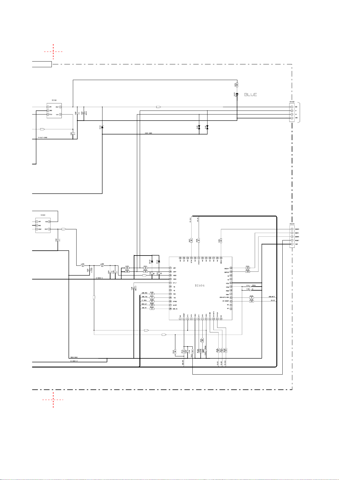
7.3. USB Block
7230-06-11
7230-02-11
CN885
YESAD182
YESAM400
YESAD143
3.3V
YESAM401
5V
YESAD141
1/4W
3.3V
5V
YESAM347
3.3V
YESAD133
3.3V
YESAD166
To
USB
MEMORY
(
)
YESAD181
YESAD181
3.3V
YESAM399
3.3V
3.3V
3.3V
CQ-C3355N USB
14

8 Schematic Diagram-2
8.1. Connector Block
7230-05-12
CN901
7230-03-11
YESAD155
5V
9V
K0H1BA000445
5V
CN971
9V
7230-02-11
YESAD165
CQ-C3355N CN
15

8.2. CD Interface Block
3.3V
3.3V
The following symbol is
shown on the schematic
diagram.
CD INTERFACE
CQ-C3355N
3.3V
3.3V
7230-02-11
16

9 Printed Circuit Board
9.1. Main/Connector Block (Top View)
17

9.2. Main/Connector Block (Bottom View)
18

9.3. Dis p lay Block
19

9.4. USB Block
20

9.5. CD Interface Block
21

10 Exploded View and Replacement Parts List
A
B
C
D
E
A
B
C
D
E
1234
1234
CQ-C3355N
2
8
< Installation Parts
Mounting Collar >
A
A
20
Main P.C.B
[7230-02-11]
AT051
CN801
AT001
AT002
PA051
CN971
21
23
12
13
11
22
10
USB P.C.B
[7230-06-11]
GC001
45
46
47
48
49
54 55
53
105
105
101
102
1
6
101
104
107
4
101
103
7
30
108
38
36
37
39
40
32
35
34
33
106
106
26
27
28
25
106
100
100
92
93
50
51
52
59
57
56
< Installation Parts
Trim Plate >
58
Display P.C.B
[7230-05-12]
31
Connector P.C.B
[7230-03-11]
CD Deck
Ass'y
29
10.1. Exploded View
22

10.2. Replacement Parts List
Notes :
1. Be sure to make you r orde rs of repl acem ent p arts acco rding to this list.
2. Important safety notice: Components, identified by
mark have special characteristics important for safety.
When replacing any of these components, use only manufacturer's specified parts.
3. Location keys in the remarks column indicates the general location of the parts shown in the exploded drawing,
as in a road map.
4. The marking (RTL) indicates that Retention Time is limited for this item. After the discontinuation of assembly in
production, the item will continue to be available for a
specific pe ri od of time . Th e re tent ion p er iod of avai lab ili ty
is dependent on the type of assembly, and in accordance
with the laws governing part and product retention. After
the end of this period, the assembly will no longer be
available.
• Order intak e period is basi cally s ix month s after t he fir st
shipment.
Ref. No. Part No. Part Name & Description Remarks
[7230-02-11] Main Block
IC's and TRANSISTORs
IC201 YESAM384 IC
IC271 C1EA00000041 IC
IC501 YESAM283 IC
IC601 YESAM402 IC
IC602 YESAM390 IC
IC650 YESAM391 IC
IC740 YESAM269 IC
IC750 YESAM267 IC
IC791 YESAM344 IC
IC801 YESAM393 IC
IC802 YESAM352 IC
PA051 YESAP413 Tuner Pack
Q054 YESAN122 Transistor
Q055 YESAN117 Transistor
Q066 YESAN132 Transistor
Q251 YESAN119 Transistor
Q261 YESAN118 Transistor
Q263 YESAN121 Transistor
Q264 YESAN121 Transistor
Q363 YESAN121 Transistor
Q364 YESAN121 Transistor
Q401 B1CBGF000005 FET
Q602 YESAN122 Transistor
Q701 YESAN126 Transistor
Q702 YESAN129 Transistor
Q704 YESAN123 Transistor
Q740 YESAN079 Transistor
Q750 YESAN079 Transistor
Q752 YESAN115 FET
Q770 YESAN087 Transistor
Q851 YESAN148 Transistor
Q871 YESAN113 Transistor
Q971 YESAN120 Transistor
Q972 YESAN118 Transistor
DIODEs
D053 YESAD119 Zener Diode
D251 YESAD155 Diode
D270 YESAD146 Diode
D271 YESAD146 Diode
D272 YESAD146 Diode
D273 YESAD146 Diode
D274 YESAD146 Diode
Ref. No. Part No. Part Name & Description Remarks
D275 YESAD146 Diode
D276 YESAD146 Diode
D277 YESAD146 Diode
D601 YESAD143 Diode
D650 YESAD144 Diode
D651 YESAD119 Zener Diode
D701 YESAD139 Diode
D702 YESAD153 Zener Diode
D703 YESAD119 Zener Diode
D704 YESAD143 Diode
D705 YESAD146 Diode
D721 YESAD167 Diode
D741 YEAD1SS133T Diode
D750 YESAD141 Diode
D760 YESAD146 Diode
D761 YESAD140 Diode
D762 YESAD167 Diode
D770 YESAD143 Diode
D771 YESAD156 Zener Diode
D791 YESAD146 Diode
D795 YESAD144 Diode
D801 YESAD181 Zener Diode
D802 YESAD181 Zener Diode
D803 YESAD181 Zener Diode
D881 YESAD183 Diode
D882 YESAD183 Diode
D883 YESAD183 Diode
D884 YESRG339 Chip, 0Ω
D885 YESAD133 Zener Diode
D886 YESAD155 Diode
D971 YESAD165 LED
D974 YESAD133 Zener Diode
D975 YESAD150 Zener Diode
D976 YESAD133 Zener Diode
D977 YESAD150 Zener Diode
D978 YESAD133 Zener Diode
D979 YESAD133 Zener Diode
D981 YESAD149 Diode
CAPACITORs
C051 YESCC478 Ceramic, 47pF 50WV
C053 YESCC482 Ceramic, 0.01µF 50WV
C055 YESCC482 Ceramic, 0.01µF 50WV
C061 YESCC447 Ceramic, 0.022µF 25WV
C062 YESCC447 Ceramic, 0.022µF 25WV
C065 YESCC481 Ceramic, 0.001µF 50WV
C066 YESCC479 Ceramic, 470pF 50WV
C067 YESCC482 Ceramic, 0.01µF 50WV
C201 YESCC556 Ceramic, 0.33µF 16WV
C202 YESCC550 Electrolytic, 3.3µF 50WV
C203 YESCC590 Electrolytic, 1µF 50WV
C204 YESCC590 Electrolytic, 1µF 50WV
C210 YESCC590 Electrolytic, 1µF 50WV
C211 YESCC546 Electrolytic, 10µF 16WV
C220 YESCC523 Ceramic, 0.1µF 16WV
C221 YESCC365 Electrolytic, 120µF 10WV
C255 YESCC549 Electrolytic, 2.2µF 50WV
C261 YESCC372 Electrolytic, 4.7µF 25WV
C262 YESCC372 Electrolytic, 4.7µF 25WV
C263 ECQV1H224JL2 Plastic Film, 0.22µF 50WV
C267 ECQV1H224JL2 Plastic Film, 0.22µF 50WV
C271 YESCC486 Ceramic, 0.0047µF 50WV
C272 YESCC486 Ceramic, 0.0047µF 50WV
C276 YESCC595 Electrolytic, 47µF 16WV
C277 YESCC452 Ceramic, 1µF 16WV
C278 YESCC593 Ceramic, 0.1µF 16WV
C279 YESCC368 Electrolytic, 2200µF 16WV
C292 YESCC482 Ceramic, 0.01µF 50WV
C301 YESCC556 Ceramic, 0.33µF 16WV
C302 YESCC550 Electrolytic, 3.3µF 50WV
C303 YESCC590 Electrolytic, 1µF 50WV
C304 YESCC590 Electrolytic, 1µF 50WV
C326 YESCC620 Electrolytic, 220µF 10WV
23
Ref. No. Part No. Part Name & Description Remarks
C361 YESCC372 Electroly tic, 4.7µF 25WV
C362 YESCC372 Electroly tic, 4.7µF 25WV
C363 ECQV1H224JL2 Plastic Film, 0.22µF 50WV
C367 ECQV1H224JL2 Plastic Film, 0.22µF 50WV
C371 YESCC486 Ceramic, 0.0047µF 50WV
C372 YESCC486 Ceramic, 0.0047µF 50WV
C375 YESCC597 Electroly tic, 10µF 16WV
C378 YESCC593 Ceramic, 0.1µF 16WV
C390 YESCC563 Ceramic, 2.2µF 10WV
C391 YESCC563 Ceramic, 2.2µF 10WV
C401 YESCC621 Electroly tic, 330µF 10WV
C402 ECQV1H683JL2 Plastic, 0.068µF 50WV
C403 YESCC562 Ceramic, 0.0068µF 50WV
C404 YESCC482 Ceramic, 0.01µF 50WV
C430 YESCC599 Electroly tic, 220µF 10WV
C501 YESCC600 Ceramic, 27pF 50WV
C502 YESCC605 Ceramic, 10pF 50WV
C505 YESCC523 Ceramic, 0.1µF 16WV
C506 YESCC442 Ceramic, 0.01µF 50WV
C507 YESCC433 Ceramic, 270pF 50WV
C508 YESCC546 Electroly tic, 10µF 16WV
C509 YESCC545 Electroly tic, 22µF 10WV
C601 YESCC571 Ceramic, 22pF 50WV
C602 YESCC602 Ceramic, 27pF 50WV
C603 YESCC480 Ceramic, 10µF 6.3WV
C604 YESCC523 Ceramic, 0.1µF 16WV
C605 YESCC523 Ceramic, 0.1µF 16WV
C606 YESCC603 Electroly tic, 1000µF 6.3WV
C607 YESCC523 Ceramic, 0.1µF 16WV
C608 YESCC430 Ceramic, 100pF 50WV
C609 YESCC452 Ceramic, 1µF 16WV
C610 YESCC442 Ceramic, 0.01µF 50WV
C611 YESCC442 Ceramic, 0.01µF 50WV
C612 YESCC442 Ceramic, 0.01µF 50WV
C613 YESCC605 Ceramic, 10pF 50WV
C614 YESCC475 Ceramic, 12pF 50WV
C615 YESCC593 Ceramic, 0.1µF 16WV
C642 YESCC452 Ceramic, 1µF 16WV
C650 YESCC442 Ceramic, 0.01µF 50WV
C701 YESCC523 Ceramic, 0.1µF 16WV
C702 YESCC523 Ceramic, 0.1
C703 YESCC452 Ceramic, 1µF 16WV
C741 YESCC379 Electroly tic, 150µF 6.3WV
C751 YESCC368 Electroly tic, 2200µF 16WV
C752 YESCC365 Electroly tic, 120µF 10WV
C753 YESCC622 Electroly tic, 47µF 6.3WV
C770 YESCC547 Electroly tic, 100µF 16WV
C791 YESCC556 Ceramic, 0.33µF 16WV
C792 YESCC548 Electroly tic, 47µF 16WV
C801 YESCC525 Ceramic, 0.0047µF 50WV
C802 YESCC442 Ceramic, 0.01µF 50WV
C803 YESCC523 Ceramic, 0.1µF 16WV
C804 YESCC523 Ceramic, 0.1µF 16WV
C805 YESCC442 Ceramic, 0.01µF 50WV
C806 YESCC441 Ceramic, 1000pF 50WV
C807 YESCC523 Ceramic, 0.1µF 16WV
C808 YESCC442 Ceramic, 0.01µF 50WV
C809 YESCC523 Ceramic, 0.1µF 16WV
C810 YESCC608 Electroly tic, 100µF 6.3WV
C811 YESCC609 Ceramic, 0.22µF 16WV
C812 YESCC527 Ceramic, 0.022µF 25WV
C813 YESCC593 Ceramic, 0.1µF 16WV
C814 YESCC523 Ceramic, 0.1µF 16WV
C815 YESCC523 Ceramic, 0.1µF 16WV
C816 YESCC544 Electroly tic, 100µF 6.3WV
C817 YESCC523 Ceramic, 0.1µF 16WV
C818 YESCC544 Electroly tic, 100µF 6.3WV
C819 YESCC523 Ceramic, 0.1µF 16WV
C820 YESCC520 Ceramic, 68pF 50WV
C821 YESCC610 Ceramic, 68pF 50WV
C822 YESCC523 Ceramic, 0.1µF 16WV
C823 YESCC523 Ceramic, 0.1µF 16WV
C824 YESCC523 Ceramic, 0.1µF 16WV
C825 YESCC452 Ceramic, 1µF 16WV
µF 16WV
Ref. No. Part No. Part Name & Description Remarks
C826 YESCC523 Ceramic, 0.1µF 16WV
C827 YESCC608 Electrolytic, 100µF 6.3WV
C828 YESCC523 Ceramic, 0.1µF 16WV
C829 YESCC523 Ceramic, 0.1µF 16WV
C830 YESCC523 Ceramic, 0.1µF 16WV
C831 YESCC544 Electrolytic, 100µF 6.3WV
C832 YESCC523 Ceramic, 0.1µF 16WV
C833 YESCC611 Electrolytic, 330µF 6.3WV
C834 YESCC523 Ceramic, 0.1µF 16WV
C835 YESCC560 Ceramic, 0.047µF 50WV
C836 YESCC608 Electrolytic, 100µF 6.3WV
C851 YESCC482 Ceramic, 0.01µF 50WV
C852 YESCC547 Electrolytic, 100µF 16WV
C853 YESCC482 Ceramic, 0.01µF 50WV
C854 YESCC538 Electrolytic, 150µF 6.3WV
C855 YESCC547 Electrolytic, 100µF 16WV
C856 YESCC523 Ceramic, 0.1µF 16WV
C859 YESCC593 Ceramic, 0.1µF 16WV
C871 YESCC593 Ceramic, 0.1µF 16WV
C872 YESCC593 Ceramic, 0.1µF 16WV
C873 YESCC482 Ceramic, 0.01µF 50WV
C874 YESCC558 Electrolytic, 5.6µF 50WV
C875 YESCC593 Ceramic, 0.1µF 16WV
C876 YESCC538 Electrolytic, 150µF 6.3WV
C877 YESCC604 Electrolytic, 47µF 6.3WV
C878 YESCC523 Ceramic, 0.1µF 16WV
C879 YESCC593 Ceramic, 0.1µF 16WV
C880 YESCC544 Electrolytic, 100µF 6.3WV
C881 YESCC544 Electrolytic, 100µF 6.3WV
C882 YESCC623 Electrolytic, 220µF 16WV
C883 YESCC623 Electrolytic, 220µF 16WV
C891 YESCC441 Ceramic, 1000pF 50WV
C895 YESCC523 Ceramic, 0.1µF 16WV
C896 YESCC430 Ceramic, 100pF 50WV
RESISTORs
J200 YESRG324 Chip, 0Ω 1/4W
J201 ERJ8GX0R00V Chip, 0Ω 1/4W
J502 YESRG339 Chip, 0Ω
J503 YESRG339 Chip, 0Ω
J602 YESRG339 Chip, 0Ω
L291 YESRG196 Chip, 0Ω 1/8W
R030 YESRG241 Chip, 0Ω 1/8W
R050 YESRG399 Chip, 5.6Ω 1/8W
R052 YESRG359 Chip, 100Ω 1/8W
R053 YESRG241 Chip, 0Ω 1/8W
R058 YESRG404 Chip, 8.2kΩ 1/8W
R060 YESRG385 Chip, 33kΩ 1/8W
R065 YESRG387 Chip, 39kΩ 1/8W
R066 YESRG442 Chip, 330kΩ 1/8W
R067 YESRG320 Chip, 2.2kΩ 1/8W
R068 YESRG319 Chip, 1kΩ 1/8W
R068 YESRG319 Chip, 1kΩ 1/8W
R070 YESRG375 Chip, 220Ω 1/8W
R101 YESRG196 Chip, 0Ω 1/8W
R102 YESRG196 Chip, 0Ω 1/8W
R201 YESRG454 Chip, 18kΩ 1/10W
R202 YESRG391 Chip, 47kΩ 1/8W
R203 YESRG320 Chip, 2.2kΩ 1/8W
R204 YESRG468 Chip, 9.1kΩ 1/10W
R205 YESRG397 Chip, 5.6kΩ 1/8W
R206 YESRG406 Chip, 9.1kΩ 1/8W
R207 YESRG241 Chip, 0Ω 1/8W
R220 YESRG319 Chip, 1kΩ 1/8W
R220 YESRG319 Chip, 1kΩ 1/8W
R221 YESRG319 Chip, 1kΩ 1/8W
R221 YESRG319 Chip, 1kΩ 1/8W
R224 YESRG241 Chip, 0Ω 1/8W
R225 YESRG231 Chip, 33kΩ 1/10W
R230 ERJ8GX0R00V Chip, 0Ω 1/4W
R240 YESRG233 Chip, 47kΩ 1/10W
R253 YESRG461 Chip, 4.3kΩ
R255 YESRG396 Chip, 560Ω 1/8W
1/10W
24
Ref. No. Part No. Part Name & Description Remarks
R256 YESRG397 Chip, 5.6kΩ 1/8W
R261 YESRG371 Chip, 180Ω 1/8W
R262 YESRG371 Chip, 180Ω 1/8W
R263 YESRG396 Chip, 560Ω 1/8W
R265 YESRG223 Chip, 10kΩ 1/10W
R266 YESRG223 Chip, 10kΩ 1/10W
R267 YESRG396 Chip, 560Ω 1/8W
R275 YESRG376 Chip, 22kΩ 1/8W
R280 YESRG365 Chip, 130Ω 1/8W
R291 YESRG241 Chip, 0Ω 1/8W
R298 YESRG391 Chip, 47kΩ 1/8W
R301 YESRG454 Chip, 18kΩ 1/10W
R302 YESRG391 Chip, 47kΩ 1/8W
R303 YESRG320 Chip, 2.2kΩ 1/8W
R304 YESRG468 Chip, 9.1kΩ 1/10W
R305 YESRG397 Chip, 5.6kΩ 1/8W
R306 YESRG406 Chip, 9.1kΩ 1/8W
R307 YESRG241 Chip, 0Ω 1/8W
R353 YESRG461 Chip, 4.3kΩ 1/10W
R361 YESRG371 Chip, 180Ω 1/8W
R362 YESRG371 Chip, 180Ω 1/8W
R363 YESRG396 Chip, 560Ω 1/8W
R365 YESRG223 Chip, 10kΩ 1/10W
R366 YESRG223 Chip, 10kΩ 1/10W
R367 YESRG396 Chip, 560Ω 1/8W
R375 YESRG527 Chip, 12kΩ 1/10W
R391 YESRG241 Chip, 0Ω 1/8W
R398 YESRG391 Chip, 47kΩ 1/8W
R399 YESRG533 Chip, 470Ω 1/4W
R401 YESRG334 Chip, 10Ω 1/8W
R402 YESRG384 Chip, 330Ω 1/8W
R403 YESRG394 Chip, 5.1kΩ 1/8W
R501 YESRG441 Chip, 2.2MΩ 1/8W
R506 YESRG223 Chip, 10kΩ
R507 YESRG223 Chip, 10kΩ 1/10W
R521 YESRG241 Chip, 0Ω 1/8W
R522 YESCC482 Ceramic, 0.01µF 50WV
R600 YESRG227 Chip, 2.2kΩ 1/10W
R601 YESRG222 Chip, 1kΩ 1/10W
R602 YESRG222 Chip, 1kΩ 1/10W
R603 YESRG222 Chip, 1kΩ 1/10W
R604 YESRG222 Chip, 1kΩ 1/10W
R605 YESRG221 Chip, 100Ω 1/10W
R606 YESRG227 Chip, 2.2kΩ 1/10W
R607 YESRG227 Chip, 2.2kΩ 1/10W
R608 YESRG227 Chip, 2.2kΩ 1/10W
R609 YESRG222 Chip, 1kΩ 1/10W
R610 YESRG222 Chip, 1kΩ 1/10W
R611 YESRG222 Chip, 1kΩ 1/10W
R612 YESRG222 Chip, 1kΩ 1/10W
R613 YESRG222 Chip, 1kΩ 1/10W
R614 YESRG222 Chip, 1kΩ 1/10W
R615 YESRG222 Chip, 1kΩ 1/10W
R617 YESRG222 Chip, 1kΩ 1/10W
R619 YESRG233 Chip, 47kΩ 1/10W
R620 YESRG233 Chip, 47kΩ 1/10W
R621 YESRG233 Chip, 47kΩ 1/10W
R622 YESRG233 Chip, 47kΩ 1/10W
R623 YESRG233 Chip, 47kΩ 1/10W
R624 YESRG222 Chip, 1kΩ 1/10W
R625 YESRG233 Chip, 47kΩ 1/10W
R626 YESRG222 Chip, 1kΩ 1/10W
R627 YESRG222 Chip, 1kΩ 1/10W
R628 YESRG360 Chip, 10kΩ 1/8W
R629 YESRG360 Chip, 10kΩ 1/8W
R630 YESRG233 Chip, 47kΩ 1/10W
R631 YESRG227 Chip, 2.2kΩ 1/10W
R633 YESRG222 Chip, 1k
R634 YESRG233 Chip, 47kΩ 1/10W
R635 YESRG221 Chip, 100Ω 1/10W
R637 YESRG391 Chip, 47kΩ 1/8W
R639 YESRG223 Chip, 10kΩ 1/10W
R641 YESRG233 Chip, 47kΩ 1/10W
R642 YESRG360 Chip, 10kΩ 1/8W
1/10W
Ω 1/10W
Ref. No. Part No. Part Name & Description Remarks
R643 YESRG222 Chip, 1kΩ 1/10W
R644 ERJ3GEY0R00V Chip, 0Ω 1/16W
R646 YESRG226 Chip, 220Ω 1/10W
R647 YESRG494 Chip, 510Ω 1/10W
R648 YESRG222 Chip, 1kΩ 1/10W
R649 YESRG463 Chip, 560kΩ 1/10W
R650 YESRG319 Chip, 1kΩ 1/8W
R650 YESRG319 Chip, 1kΩ 1/8W
R651 YESRG233 Chip, 47kΩ 1/10W
R652 YESRG396 Chip, 560Ω 1/8W
R653 YESRG222 Chip, 1kΩ 1/10W
R654 YESRG319 Chip, 1kΩ 1/8W
R654 YESRG319 Chip, 1kΩ 1/8W
R655 YESRG233 Chip, 47kΩ 1/10W
R656 ERJ3GEY0R00V Chip, 0Ω 1/16W
R657 YESRG319 Chip, 1kΩ 1/8W
R657 YESRG319 Chip, 1kΩ 1/8W
R658 YESRG391 Chip, 47kΩ 1/8W
R659 ERJ3GEY0R00V Chip, 0Ω 1/16W
R660 YESRG319 Chip, 1kΩ 1/8W
R660 YESRG319 Chip, 1kΩ 1/8W
R661 YESRG319 Chip, 1kΩ 1/8W
R661 YESRG319 Chip, 1kΩ 1/8W
R662 YESRG233 Chip, 47kΩ 1/10W
R663 YESRG319 Chip, 1kΩ 1/8W
R663 YESRG319 Chip, 1kΩ 1/8W
R664 YESRG319 Chip, 1kΩ 1/8W
R664 YESRG319 Chip, 1kΩ 1/8W
R665 YESRG391 Chip, 47kΩ 1/8W
R666 YESRG391 Chip, 47kΩ 1/8W
R667 YESRG319 Chip, 1kΩ 1/8W
R668 YESRG319 Chip, 1kΩ 1/8W
R668 YESRG319 Chip, 1kΩ 1/8W
R669 ERJ3GEY0R00V Chip, 0Ω
R671 YESRG319 Chip, 1kΩ 1/8W
R671 YESRG319 Chip, 1kΩ 1/8W
R672 YESRG319 Chip, 1kΩ 1/8W
R672 YESRG319 Chip, 1kΩ 1/8W
R673 YESRG358 Chip, 470Ω 1/10W
R674 YESRG222 Chip, 1kΩ 1/10W
R675 YESRG222 Chip, 1kΩ 1/10W
R676 YESRG221 Chip, 100Ω 1/10W
R690 YESRG319 Chip, 1kΩ 1/8W
R690 YESRG319 Chip, 1kΩ 1/8W
R691 YESRG359 Chip, 100Ω 1/8W
R692 YESRG359 Chip, 100Ω 1/8W
R693 YESRG359 Chip, 100Ω 1/8W
R694 YESRG359 Chip, 100Ω 1/8W
R695 YESRG361 Chip, 100kΩ 1/8W
R696 YESRG361 Chip, 100kΩ 1/8W
R697 YESRG361 Chip, 100kΩ 1/8W
R698 YESRG241 Chip, 0Ω 1/8W
R702 YESRG366 Chip, 13kΩ 1/8W
R703 YESRG362 Chip, 11kΩ 1/8W
R704 YESRG231 Chip, 33kΩ 1/10W
R705 YESRG224 Chip, 100kΩ 1/10W
R710 YESRG222 Chip, 1kΩ 1/10W
R711 YESRG358 Chip, 470Ω 1/10W
R712 YESRG376 Chip, 22kΩ 1/8W
R713 YESRG388 Chip, 4.3kΩ 1/8W
R714 YESRG404 Chip, 8.2kΩ 1/8W
R740 YESRG361 Chip, 100kΩ 1/8W
R751 YESRG391 Chip, 47kΩ 1/8W
R752 YESRG367 Chip, 1.5kΩ 1/8W
R753 YESRG241 Chip, 0Ω 1/8W
R764 YESRG324 Chip, 0Ω 1/4W
R770 YESRG396 Chip, 560Ω 1/8W
R771 YESRG196 Chip, 0
R772 YESRG196 Chip, 0Ω 1/8W
R773 YESRG396 Chip, 560Ω 1/8W
R791 YESRG500 Chip, 2.4kΩ 1/10W
R792 YESRG501 Chip, 27kΩ 1/10W
R800 ERJ8GX0R00V Chip, 0Ω 1/4W
R801 YESRG229 Chip, 330Ω 1/10W
1/16W
Ω 1/8W
25

Ref. No. Part No. Part Name & Description Remarks
R802 ERJ3GEY0R00V Chip, 0Ω 1/16W
R803 ERJ3GEY0R00V Chip, 0Ω 1/16W
R804 YESRG232 Chip, 4.7kΩ 1/10W
R805 YESRG232 Chip, 4.7kΩ 1/10W
R806 YESRG503 Chip, 680Ω 1/10W
R807 YESRG534 Chip, 3.3MΩ 1/10W
R808 YESRG503 Chip, 680Ω 1/10W
R809 YESRG504 Chip, 68kΩ 1/10W
R810 YESRG223 Chip, 10kΩ 1/10W
R811 YESRG221 Chip, 100Ω 1/10W
R812 YESRG317 Chip, 3.9kΩ 1/10W
R813 YESRG317 Chip, 3.9kΩ 1/10W
R814 YESRG484 Chip, 3.9kΩ 1/8W
R815 YESRG222 Chip, 1kΩ 1/10W
R816 YESRG506 Chip, 27kΩ 1/10W
R817 YESRG319 Chip, 1kΩ 1/8W
R817 YESRG319 Chip, 1kΩ 1/8W
R818 YESRG319 Chip, 1kΩ 1/8W
R818 YESRG319 Chip, 1kΩ 1/8W
R819 YESRG431 Chip, 22Ω 1/8W
R820 YESRG230 Chip, 3.3kΩ 1/10W
R821 YESRG330 Chip, 150Ω 1/10W
R822 YESRG224 Chip, 100kΩ 1/10W
R823 ERJ3GEY0R00V Chip, 0Ω 1/16W
R824 YESRG507 Chip, 47Ω 1/10W
R825 YESRG448 Chip, 10Ω 1/10W
R826 ERJ3GEY0R00V Chip, 0Ω 1/16W
R827 ERJ3GEY0R00V Chip, 0Ω 1/16W
R828 YESRG223 Chip, 10kΩ 1/10W
R829 YESRG319 Chip, 1kΩ 1/8W
R829 YESRG319 Chip, 1kΩ 1/8W
R830 YESRG436 Chip, 68kΩ 1/8W
R832 YESRG376 Chip, 22kΩ 1/8W
R833 ERJ3GEY0R00V Chip, 0Ω
R834 ERJ3GEY0R00V Chip, 0Ω 1/16W
R835 YESRG492 Chip, 2.7kΩ 1/4W
R836 YESRG359 Chip, 100Ω 1/8W
R837 YESRG196 Chip, 0Ω 1/8W
R851 YESRG499 Chip, 22kΩ 1/4W
R852 YESRG391 Chip, 47kΩ 1/8W
R853 YESRG376 Chip, 22kΩ 1/8W
R854 YESRG368 Chip, 15kΩ 1/8W
R855 YESRG360 Chip, 10kΩ 1/8W
R856 YESRG428 Chip, 16kΩ 1/8W
R857 YESRG385 Chip, 33kΩ 1/8W
R858 YESRG385 Chip, 33kΩ 1/8W
R859 YESRG435 Chip, 6.2kΩ 1/8W
R860 YESRG401 Chip, 6.8kΩ 1/8W
R861 YESRG435 Chip, 6.2kΩ 1/8W
R862 YESRG505 Chip, 10kΩ 1/4W
R871 YESRG389 Chip, 470Ω 1/8W
R872 YESRG319 Chip, 1kΩ 1/8W
R872 YESRG319 Chip, 1kΩ 1/8W
R873 YESRG319 Chip, 1kΩ 1/8W
R873 YESRG319 Chip, 1kΩ 1/8W
R874 YESRG512 Chip, 3.3Ω 1/4W
R875 YESRG513 Chip, 33Ω 1/4W
R880 YESRG361 Chip, 100kΩ 1/8W
R881 YESRG391 Chip, 47kΩ 1/8W
R882 YESRG319 Chip, 1kΩ 1/8W
R882 YESRG319 Chip, 1kΩ 1/8W
R883 YESRG359 Chip, 100Ω 1/8W
R884 YESRG359 Chip, 100Ω 1/8W
R885 YESRG241 Chip, 0Ω 1/8W
R886 YESRG241 Chip, 0Ω 1/8W
R887 YESRG241 Chip, 0Ω 1/8W
R889 YESRG484 Chip, 3.9kΩ 1/8W
R890 YESRG391 Chip, 47k
R891 YESRG391 Chip, 47kΩ 1/8W
R892 YESRG391 Chip, 47kΩ 1/8W
R893 YESRG372 Chip, 1.8kΩ 1/8W
R894 YESRG319 Chip, 1kΩ 1/8W
R894 YESRG319 Chip, 1kΩ 1/8W
R895 YESRG241 Chip, 0Ω 1/8W
1/16W
Ω 1/8W
Ref. No. Part No. Part Name & Description Remarks
R896 YESRG241 Chip, 0Ω 1/8W
R897 YESRG359 Chip, 100Ω 1/8W
R898 YESRG241 Chip, 0Ω 1/8W
R899 YESRG241 Chip, 0Ω 1/8W
R900 YESRG359 Chip, 100Ω 1/8W
R901 YESRG359 Chip, 100Ω 1/8W
R971 YESRG315 Chip, 180kΩ 1/10W
R972 YESRG319 Chip, 1kΩ 1/8W
R972 YESRG319 Chip, 1kΩ 1/8W
R974 YESRG222 Chip, 1kΩ 1/10W
R975 YESRG319 Chip, 1kΩ 1/8W
R975 YESRG319 Chip, 1kΩ 1/8W
R976 YESRG222 Chip, 1kΩ 1/10W
R977 YESRG222 Chip, 1kΩ 1/10W
R978 YESRG222 Chip, 1kΩ 1/10W
R979 YESRG373 Chip, 180kΩ 1/8W
R981 YESRG222 Chip, 1kΩ 1/10W
R982 YESRG319 Chip, 1kΩ 1/8W
R983 YESRG361 Chip, 100kΩ 1/8W
R984 YESRG222 Chip, 1kΩ 1/10W
R985 YESRG224 Chip, 100kΩ 1/10W
R986 YESRG399 Chip, 5.6Ω 1/8W
R989 YESRG315 Chip, 180kΩ 1/10W
R990 YESRG222 Chip, 1kΩ 1/10W
OCNNECTORs
CN250 YESAE441 RCA Jack, 2P
CN251 YESAJ07031 RCA Wire (AUX1-IN)
CN650 YESAE411 Connector, 13P
CN701 YESAE351 Connector, 16P
CN801 YESAE443 Connector, 22P
CN971 YESAE446 Connector, 14P
COILs
L050 YESLQ028 Inductor
L051 YESLQ035 Inductor
L201 YESLQ027 Inductor
L501 YESLQ044 Inductor
L601 YESLQ044 Inductor
L701 YESLT030 Inductor
L710 YESLQ012 Inductor
L801 YESLQ048 Inductor
L802 YESLQ048 Inductor
L881 YESLQ059 Inductor
L971 YESLQ027 Inductor
CRYSTALs
XL501 YESXL039 Crystal
XL601 YESXL041 Crystal
XL602 YESXL042 Crystal
XL801 YESXL038 Crystal
POSISTOR
PH701 YESRTD011 Posistor
SERGE PROTECTOR / VARI STOR
Z050 YESRTD014 Serge Protector
Z701 YESRTD012 Varistor
SWITCH
SW971 YEAS08042 Switch
[7230-06-11] USB Block
IC's
IC101 YESAM399 IC
IC102 YESAM400 IC
26

Ref. No. Part No. Part Name & Description Remarks
IC103 YESAM401 IC
IC104 YESAM347 IC
DIODEs
D111 YESAD181 Zener Diode
D1 12 YESAD181 Zener Diode
D141 YESAD182 Zener Diode
D142 YESAD143 Diode
D143 YESAD141 Diode
D161 YESAD133 Zener Diode
D170 YESAD166 LED
Ref. No. Part No. Part Name & Description Remarks
R162 YESRG233 Chip, 47kΩ 1/10W
R143 YESRG063 Chip, 24kΩ 1/10W
R144 YESRG466 Chip, 8.2kΩ 1/10W
R145 YESRG530 Chip, 180Ω 1/4W
R146 YESRG531 Chip, 56kΩ 1/10W
R147 YESRG532 Chip, 10kΩ 1/10W
R161 YESRG196 Chip, 0Ω 1/8W
R168 YESRG196 Chip, 0Ω 1/8W
R170 YESRG378 Chip, 240Ω 1/8W
R171 YESRG241 Chip, 0Ω 1/8W
R172 YESRG241 Chip, 0Ω 1/8W
R173 YESRG241 Chip, 0Ω 1/8W
CAPACITORs
C101 YESCC616 Ceramic, 5pF 50WV
C102 YESCC616 Ceramic, 5pF 50WV
C148 YESCC616 Ceramic, 5pF 50WV
C103 YESCC617 Electroly tic, 22µF 6.3WV
C104 YESCC563 Ceramic, 2.2µF 10WV
C105 YESCC523 Ceramic, 0.1µF 16WV
C143 YESCC523 Ceramic, 0.1µF 16WV
C145 YESCC523 Ceramic, 0.1µF 16WV
C153 YESCC523 Ceramic, 0.1µF 16WV
C154 YESCC523 Ceramic, 0.1µF 16WV
C161 YESCC523 Ceramic, 0.1µF 16WV
C162 YESCC523 Ceramic, 0.1µF 16WV
C106 YESCC618 Electroly tic, 2.2µF 35WV
C108 YESCC480 Ceramic, 10µF 6.3WV
C150 YESCC480 Ceramic, 10µF 6.3WV
C109 YESCC609 Ceramic, 0.22µF 16WV
C110 YESCC443 Ceramic, 1500pF 50WV
C111 YESCC443 Ceramic, 1500pF 50WV
C141 YESCC619 Electroly tic, 22µF 16WV
C142 YESCC452 Ceramic, 1µF 16WV
C146 YESCC520 Ceramic, 68pF 50WV
C147 YESCC430 Ceramic, 100pF 50WV
C152 YESCC522 Ceramic, 1µF 16WV
C163 YESCC460 Electroly tic, 10µF 16WV
RESITORs
L105 YESRG324 Chip, 0Ω 1/4W
R148 YESRG324 Chip, 0Ω 1/4W
R152 YESRG324 Chip, 0Ω 1/4W
R101 YESRG458 Chip, 33Ω 1/10W
R102 YESRG458 Chip, 33Ω 1/10W
R103 YESRG356 Chip, 15kΩ 1/10W
R104 YESRG356 Chip, 15kΩ 1/10W
R105 ERJ3GEY0R00V Chip, 0Ω 1/16W
R106 YESRG221 Chip, 100Ω 1/10W
R109 YESRG221 Chip, 100Ω 1/10W
R114 YESRG221 Chip, 100Ω 1/10W
R116 YESRG221 Chip, 100Ω
R117 YESRG221 Chip, 100Ω 1/10W
R118 YESRG221 Chip, 100Ω 1/10W
R119 YESRG221 Chip, 100Ω 1/10W
R121 YESRG221 Chip, 100Ω 1/10W
R123 YESRG221 Chip, 100Ω 1/10W
R124 YESRG221 Chip, 100Ω 1/10W
R125 YESRG221 Chip, 100Ω 1/10W
R107 YESRG222 Chip, 1kΩ 1/10W
R110 YESRG222 Chip, 1kΩ 1/10W
R120 YESRG222 Chip, 1kΩ 1/10W
R166 YESRG222 Chip, 1kΩ 1/10W
R108 YESRG316 Chip, 22Ω 1/10W
R111 ERJ8GX0R00V Chip, 0Ω 1/4W
R112 ERJ8GX0R00V Chip, 0Ω 1/4W
R113 YESRG223 Chip, 10kΩ 1/10W
R115 YESRG229 Chip, 330Ω 1/10W
R126 YESRG431 Chip, 22Ω 1/8W
R127 YESRG431 Chip, 22Ω 1/8W
R141 YESRG355 Chip, 1MΩ 1/10W
R142 YESRG233 Chip, 47kΩ 1/10W
1/10W
CONNECTORs
CN101 YESAE401 Connector, 24P
CN102 YESAE445 USB Jack
COILs
L101 YESLQ057 Inductor
L102 YESLQ057 Inductor
L104 YESLQ058 Inductor
CRYSTAL
XL101 YESXL043 Crystal
VARISTORs
Z115 YESRTD015 Varistor
Z116 YESRTD015 Varistor
[7230-05-12] Display Block
IC's and TRANSISTORs
IC901 C0HBA0000195 IC
IC905 YESAM264 IC
Q930 YESAN146 Transistor
DIODEs
D901 YESAD166 LED
D902 YESAD143 Diode
D970 YESAD143 Diode
D911 YESAD150 Zener Diode
D913 YESAD150 Zener Diode
D912 YESAD147 Zener Diode
D915 YESAD133 Zener Diode
D921 YESAD165 LED
D922 YESAD165 LED
D923 YESAD165 LED
D924 YESAD165 LED
D925 YESAD165 LED
D926 YESAD165 LED
D927 YESAD165 LED
D928 YESAD165 LED
D929 YESAD165 LED
D930 YESAD165 LED
D931 YESAD165 LED
D932 YESAD165 LED
D933 YESAD165 LED
D934 YESAD165 LED
D935 YESAD180 LED
D972 YESAD119 Zener Diode
CAPACITORs
C907 YESCC441 Ceramic, 1000pF 50WV
C908 YESCC523 Ceramic, 0.1µF 16WV
C911 YESCC523 Ceramic, 0.1µF 16WV
C912 YESCC523 Ceramic, 0.1µF 16WV
C913 YESCC521 Ceramic, 680pF 50WV
27
Ref. No. Part No. Part Name & Description Remarks
C914 YESCC568 Ceramic, 1µF 25WV
Ref. No. Part No. Part Name & Description Remarks
CN991 YESAE377 Connector, 14P
RESISTORs
R901 YESRG449 Chip, 1.1kΩ 1/10W
R902 YESRG526 Chip, 620Ω 1/8W
R903 YESRG358 Chip, 470Ω 1/10W
R904 YESRG222 Chip, 1kΩ 1/10W
R905 YESRG222 Chip, 1kΩ 1/10W
R906 YESRG222 Chip, 1kΩ 1/10W
R909 YESRG222 Chip, 1kΩ 1/10W
R908 YESRG241 Chip, 0Ω 1/8W
R910 YESRG227 Chip, 2.2kΩ 1/10W
R951 YESRG227 Chip, 2.2kΩ 1/10W
R911 YESRG234 Chip, 4.7Ω 1/10W
R912 YESRG233 Chip, 47kΩ 1/10W
R915 YESRG223 Chip, 10kΩ 1/10W
R916 YESRG429 Chip, 1Ω 1/8W
R921 YESRG389 Chip, 470Ω 1/8W
R970 YESRG389 Chip, 470Ω 1/8W
R922 YESRG386 Chip, 360Ω 1/8W
R924 YESRG386 Chip, 360Ω 1/8W
R925 YESRG386 Chip, 360Ω 1/8W
R923 YESRG393 Chip, 510Ω 1/8W
R935 YESRG488 Chip, 220Ω 1/4W
R952 YESRG232 Chip, 4.7kΩ 1/10W
R971 YESRG396 Chip, 560Ω 1/8W
CONNECTOR
CN901 YESAE376 Connector, 14P
SWITCHes
SW901 YESAS123 Switch
SW902 K0H1BA000445 Switch
SW903 K0H1BA000445 Switch
SW904 K0H1BA000445 Switch
SW905 K0H1BA000445 Switch
SW906 K0H1BA000445 Switch
SW907 K0H1BA000445 Switch
SW908 K0H1BA000445 Switch
SW909 K0H1BA000445 Switch
SW910 K0H1BA000445 Switch
SW911 K0H1BA000445 Switch
SW912 K0H1BA000445 Switch
SW913 K0H1BA000445 Switch
SW914 K0H1BA000445 Switch
SW915 K0H1BA000445 Switch
SW916 K0H1BA000445 Switch
LCD
LD901 YESXDCM040 LCD
[7230-03-11] Connector Block
DIODEs
D991 YESAD165 LED
D995 YESAD155 Diode
RESISTORs
J991 YESRG324 Chip, 0Ω 1/4W
J992 YESRG324 Chip, 0Ω 1/4W
J993 YESRG324 Chip, 0Ω
J994 YESRG324 Chip, 0Ω 1/4W
J995 YESRG324 Chip, 0Ω 1/4W
R991 YESRG222 Chip, 1kΩ 1/10W
CONNECTORs
CN990 YESAE447 Connector, 14P
1/4W
SWITCH
SW990 K0H1BA000445 Switch
Accessories
PRINTINGS
INSTALLATION PARTS
MECHANICAL PARTS
MISCELLANEOUS
AT001 YESAT01031 Earth Terminal
AT002 YESAT01031 Earth Terminal
AT051 YM104C700ZA Antenna Receptacle
GC001 YESFX005176 Ground Contactor (Bottom)
1 YESFA01073 Main Chassis
2 YESFX005155 Ground Contactor
4 YESFF01087 Heat Sink
6 YESFR01019 RCA Cap
7 YESFA05037 Bottom Cover
8 YESFX005173 Ground Contactor
10 YESAP550 USB PCB w/Components (w/Bracket,
11 YESFX021152 USB Bracket
12 YESFA13024 USB Shield Plate
13 YESFX999095 USB Holder
20 YESAP548 Main PCB w/Components RTL
21 YESFA08058 Rear Plate
22 YESFX007027 RCA Bush
23 YESFX021140 Regulator Bracket
25 YESFC02274 Escutcheon
26 YESFE13220 Button (Eject)
27 YESFS01092 Dust Felt
28 YESFX999066 Bracket Arm Ass'y
29 YESFX001042 CD Indicator
30 YESFX999096 Hook Bracket Ass'y
31 YESAP551 Connector PCB w/Components RTL
32 YESFE13221 Button, Detect
33 YESFX999065 Guide, Detect Button
34 YESFX005157 Spring, Return
35 YESFX005158 Spring, Guide
36 YEFX999097 USB Front Cover
37 YESFC04030 USB Panel
38 YESFX005174 USB Panel Spring
39 YESFE13306 Button (OPEN)
40 YESFX005175 Spring, Open Button
45 YESSDF0206 Removable Face Plate Unit RTL
46 YESFE13287 Button (SRC)
47 YESFE13288 Button (BAND T DOWN)
48 YESFE13289 Button (SQ UP)
49 YESFE13290 Button (DISP)
50 YESFE13291 Button (TUNE UP)
51 YESFE13292 Button (MUTE DOWN)
52 YESFE13293 Button (PRESET)
53 YESFA13025 Rear Cover
YEFM285925 Operating Instructions
YEFM262785 System Upgrade Guidebook
YEFM294293 Installation Instructions (English, Ger-
YEFM294294 Installation Instructions (Swedish, Ital-
YEFM294295 Installation Instructions (Polish, Czech,
YEAJ02874 Power Connector
YEP0FZ5699 Installation kit (Lock Cancel Plate,
YEFX0217263A Mounting Collar
YEFC051011 Trim Plate
YEFA134246 Removable Face Plate Case
man, French, Dutch)
ian, Spanish, Danish)
Hungarian, Russian)
Mounting Bolt, ISO Antenna Adapter)
Shield Plate, Holder)
RTL
28

Ref. No. Part No. Part Name & Description Remarks
54 YESFX999068 Shaft Collar
55 YESFX005135 Spring
56 YESFE02031 VOL Knob
57 YESFX005138 Knob Spring
58 YESAP549 Display PCB w/Components RTL
59 YESFC02271 Detachable Face Ass'y
92 YESFM01087 Laser Seal A
93 YESFM01088 Laser Seal B
100 Y ESJS 0 1189 Screw, 2.6*4.0
101 YESJS01188 Bind S Tite, 2.6*5.0
102 YESJT03074 Bind Tapping, 2.6*8
103 Y ESJS 0 1190 Screw, 2.6 * 6.0
104 YESJS01187 Bind Screw, 2.6 * 10
105 YESJT03075 Tapping Screw, 2.0*8.0
106 YESJT03076 Tapping Screw, 2*6
107 YESJS01203 Bind Screw, 2.6*6
108 Y ESJS 0 120 5 Cup Scew 2x5
29

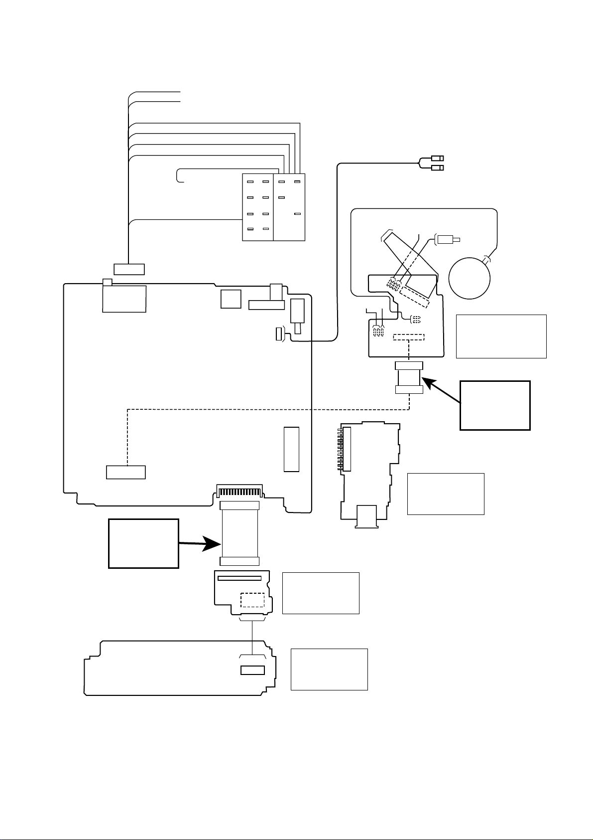
10.3. Exploded View [CD Deck]
30
10.4. CD PLAYER PARTS LIST
Notes :
1. Be sure to make you r orde rs of repl acem ent p arts acco rding to this list.
2. Important safety notice: Components, identified by
mark have special characteristics important for safety.
When replacing any of these components, use only manufacturer's specified parts.
3. Location keys in the remarks column indicates the general location of the parts shown in the exploded drawing,
as in a road map.
4. The marking (RTL) indicates that Retention Time is limited for this item. After the discontinuation of assembly in
production, the item will continue to be available for a
specific pe ri od of time . Th e re tent ion p er iod of avai lab ili ty
is dependent on the type of assembly, and in accordance
with the laws governing part and product retention. After
the end of this period, the assembly will no longer be
available.
• Order intak e period is basi cally s ix month s after t he fir st
shipment.
Ref. No. Part No. Part Name & Description Remarks
[3032-14-50] CD Interface Block
CAPACITOR
C1 YESCC439 Ceramic, 0.1µF 25WV
RESISTOR
R1 YESRG222 Chip, 1kΩ 1/10W
CONNECTORs
CN1 YESAE439 Connector, 22P
CN2 YESAE415 Connector, 16P
MECHANICAL PARTS
MISCELLANEOUS
1 YESFX046136 Frame
2 YESFX046137 Top Cover
3 YERFS04003 Damper F
4 YERFS04004 Damper R
11 YESFA01075 Chassis Rivet Ass'y
12 YER FX04 600 1 Change Plate Rivet Ass'y
13 YERFX007001 Clamper Ass'y
14 YESAK01051 Spindle Motor Ass'y
15 YERFX046002 Clamper Arm
16 YERFX005001 Change Gear Spring
17 YERFX03001 Change Gear 2
18 YERFX03002 Feed Gear
19 YERFX03003 Feed Rack
20 YERFX046003 Changer Lock Lever
21 YERFW04001 Feed Switch Holder
22 YERFW04002 Pick-up Shaft Holder
23 YERFX005002 Clamper Sub Spring
24 YERFW04003 FD Sub Holder
25 YESF X 046 13 9 Top Plate
26 YER FX04 600 4 Select Lock Arm
27 YERFX046006 Slide Hook
28 YERFW01001 Pick-up Shaft
29 YERFX005003 Clamper Arm Spring
30 YERFX005004 Select Lock Arm Spring
31 YERFX005013 Suspension Spring
32 YESF X046 140 Select Arm R
33 YER FX03 004 Link Plate
34 YESF X005137 Link Plate Spring
35 YERFS01001 Cushion F
Ref. No. Part No. Part Name & Description Remarks
36 YERFS01002 Cushion R
37 YERFX005014 Feed Spring Plate
38 YERFX046005 Trigger Arm
43 YERFX046008 Select Plate L
44 YERFX046009 Select Plate R
45 YERFX046010 Select Piece L
46 YERFX046011 Select Piece R
61 YESSZ1093 Optical Pick-up Ass'y
62 YERAS0001 Detection Switch
71 YESAP531 CD Interface PCB w/Components RTL
72 YESFX046176 Mode Switch
73 YESAJ02017 Loding Motor Wire
73 YESAJ02017 Loding Motor Wire
74 YESAJ07015 Mode Switch Wire
77 YERFX999001 Wire Clamper M
78 YESFX024021 Wire Tube SPM
79 YESFX024022 Wire Tube MSW
81 YERFX03005 Roller Shaft Ass'y
82 YERFX046012 Loading Gear Plate Rivet Ass'y
83 YERFX046013 Loading Plate Ass'y
84 YESFX046173 Lock Arm Rivet Ass'y
85 YESAK01042 LOADING/FEED Motor Ass'y
86 YERFX03006 Loading Gear 1
87 YERFX03007 Loading Gear 2
88 YERFX03008 Loading Gear 3
89 YERFX03009 Loading Gear 4
90 YERFX03010 Loading Gear 5
91 YERFX03011 Loading Gear 6
92 YERFX03012 Loading Gear 7
93 YESFW05023 Roller Guide(N)
94 YERFX005007 Roller Guide Spring
95 YERFX046015 Disc Stopper Arm
96 YERFX005008 Disc Stop Arm Spring
97 YER FX0 46016 LD Gear Bracket
98 YESFX046174 L Slide Plate
99 YERFX005009 Loading Plate Spring
100 YESFX046150 Loading Roller
101 YESJS01175 Collar Screw
111 YERJT01001 Tapping Screw, 2*3
112 YERJT01002 Tapping Screw, 2*4
113 YEJT03117 Tapping Bind Screw, 2*4
114 YERJS01002 Camera Screw, 1.7*1.8
115 YERJS01003 Camera Screw, 2*2
116 YERJS01004 Camera Tapping Screw 1.7*5
118 YESJS01148 Screw, 2*4
121 YERJW01001 P Washer, 3.5*8*0.3
122 YESJW01041 Washer 2.05*4.2*0.2
123 YERJW01003 Lumilar Washer 3.1*6*0.1
124 YEJE01028 E Ring S 1.5
125 YERJW01005 P Washer, 2.1*4*0.13
31

11 Schematic Diagram for Printing with A4 Size
11.1. Main Block (Left Side)
7230-02-11
FM
1
2
3
4
5
6
1.2
7
7.8
8
7.8
9
10
11
YESAP413
AM
FM
AM
12
0
0
3.5
3.5
13
0
0
3.5
3.5
14
0
0
0
0
15
-
-
0
0
16
-
-
0
0
17
1.3
4.9
4.8
18
7.8
0
0
19
0.5
0
0
20
0
0
-
-
21
0
0
-
-
0
0
7.8
7.9
YESAN117
8V
0
0
YESAN122
YESAN087
7.9
8.5
YESAD143
(C)
0
5V
0
L
0
9.1
YESAD156
YESAN132
2.3
YESAN122
0
0
4.8
R
YESAD119
9V
1.9
1.3
4.7
2.3
2.9
YESAM283
YESAN119
4.7
0
4.6
L
R
0
4.3
L
R
4.3
4.3
R
L
L
L
R
R
L
YESAN118
0
0
0
L
4.8
8.6
4.8
8.7
4.3
YESAM384
4.3
4.3
4.3
4.2
4.3
R
L
R
0
0
0
YESAN121
0
0
YESAN121
0
0
0
YESAN121
0
0
0
R
YESAN121
0
L
R
4.3
4.3
4.3
0.6
4.2
4.2
1/4W
YESAD155
R
L
L
L
9V
0
0
9V
5V
R
R
R
R
L
R
L
0
0
4.8
4.8
0
4.8
0
4.8
4.8
YESAM391
4.8
0
4.2
0.4
0
5V
L
L
R
R
YESAD144
5V
5V
2.5
0
2.2
4.8
2.4
YESAD150
7230-06-11
0
4.8
YESAN118
YEAS08042
YESAD133
5V
1V/DIV,10us/DIV
YESAD143
YESAM402
2V/DIV,20ms/DIV
0.2V/DIV,10us/DIV
5V
5V
1.3
2.3
0
YESAD155
B1CBGF000005
CN101
YESAD183
YESAD183 YESAD183
YESAD133
YESAD133
YESAD133
7230-03-11
YESAD133
CN990
5V
4.6
YESAN120
0
YESAD150
4.9
5V
5V
4.5
YESAD149
9V
YESAD165
5V
YESAM390
2V/DIV,20ms/DIV
0.5V/DIV,10us/DIV
2V/DIV,0.2ms/DIV
0
4.8
4.8
2V/DIV,20ms/DIV
2V/DIV,50ms/DIV
2V/DIV,20ms/DIV
2V/DIV,20ms/DIV
2V/DIV,0.5ms/DIV
2V/DIV,0.5s/DIV
5V
9V
32

11.2. Main Block (Right Side)
7230-02-11
5V
5V
YESAD139
YESAD119
YESAD146
5V
5V
5V
9V
4.7
9V
YESAN123
9V
0
0
YESAD140
YESAD167
YESAN079
4.9
5.5
YEAD1SS133T
YESAN079
4.8
8V
4.9
4.9
YESAN126
YESAD146
5.4
4.9
4.9
0
YESAD153
13.3
13.3
4.5
9V
5V
YESAD146
YESAN129
YESAN115
5V
0
0
13.3
13.3
13.3
4.8
YESAM269
4.9
YESAM344
0
0.8
0
0
0
0
YESAM267
9.1
13.0
0
13.0
YESAD141
13.3
0
0
4.8
4.8
0
4.8
4.8
4.8
YESAM391
0
4.8
0
4.2
0.4
0
YESAD119
5V
L
L
R
R
YESAD144
5V
5V
5V
L
R
L
0
6.2
4.5
L
R
L
3.3
3.3
3.2
3.3
0
1.5
3.3V
0
0
0
5V
R
0
1.6
3.3V
C1EA00000041
0
0
0
6.2
YESAD146
1.6
0
6.2
6.2
4.8
6.3
13.3
L
R
L
R
YESAD146
YESAD146
YESAD146
YESAD146
YESAD146
4.8
0
4.8
0
0
3.3
4.8
YESAM393
0.4
0
1.6
1.6
2.6
1.6
L
L
R
R
R
R
L
L
1/4W
0
0
0
0
3.3
1.6
3.3
0
3.3
1.5
0
3.3
3.3
0
0
4.8
3.3
3.2
0
2.5
0
1.7
1.7
1.8
1.8
3.2
3.2
1.6
3.2
0.3
3.3V
0
0
YESAD143
YESAD167
YESAD144
3.3V
3.3V
3.3V
0
0
3.3
3.3
6.2
3.3
16V47
3.3
3.3
YESAD181
YESAD181
YESAD181
3.3V
8.0
L
R
YESAD146
YESAD146
9V
9V
5V
5V
0
0
0
6.2
6.2
13.3
R
L
16V10
3.3
3.3
3.3
3.1
1.6
1.6
1.6
1.9
1.6
1.9
1.6
1.9
1.6
2V/DIV,0.5s/DIV
3.3V
5V
5V
3032-14-50
CN1
5V
9V
1/4W
YESAN113
0.1
3.2
1/4W
3.2
3.3V
3.3V
5V
9V
1.3
0.9
1.0
1/4W
1.2
1.6
8.4
1/4W
3.3V
8.4
7.8
3.3
YESAN148
8V
0
0
4.8
1.6
1.7
1.7
1.2
1.7
8.4
YESAM352
1.3
1.3
1.3
1.3
1.3
8V
1.7
7.8
1.7
1.7
8.4
1.3
1.3
1.3
CQ-C3355N MAIN
33

11.3. Display Block ( Le ft Side)
04
04
04
7230-05-12
1.1
0
YESAD166
YESAD165
YESAD165
YESAD165
0.7
YESAN146
YESAD165
YESAD165
YESAD165
YESAD143
YESAD133
YESAD165
YESAD165
7230-03-11
CN991
To
YESAD165
YESAD165YESAD165
YESAD165YESAD165
YESAD165
K0H1BA000445
YESAM264
YESAS123
4.804.8
9V
5V
5V
9V
K0H1BA000445
K0H1BA000445
K0H1BA000445
K0H1BA000445
K0H1BA000445
K0H1BA000445
K0H1BA000445 K0H1BA00
K0H1BA000445 K0H1BA00
K0H1BA000445
K0H1BA00
5V
YESAD180
YESAD150
9V
1/4W
YESAD143
YESAD119
9V
5V
34

11.4. Display Block (R igh t Side)
K
K
K
K
7230-05-12
0H1BA000445
0H1BA000445
0H1BA000445
0H1BA000445
K0H1BA000445
K0H1BA000445 K0H1BA000445
K0H1BA000445 K0H1BA000445 K0H1BA000445
K0H1BA000445
K0H1BA000445
K0H1BA000445
YESAD147
YESAD150
9V
5V
2.4
2.4
2.4
C0HBA0000195
2V / DIV, 2ms / DIV
2.4
2.4
2.4
2.4
2.4
2.4
1V / DIV, 2ms / DIV
2.4
2.4
2.4
2.4
2.4
4.8
4.8
2.4
2.4
2.4
2V / DIV, 2ms / DIV
1V / DIV, 2ms / DIV
2.4
2.4
4.8
4.8
0
0
0
0
0
2V / DIV, 10µs / DIV
0
5V
4.8
3.1
1.6
0
3.8
4.8
0
5.0
4.8
2V / DIV, 5ms / DIV
4.7
2V / DIV, 2ms / DIV
2.4
2.4
2.4
2.4
2.4
2.4
2.4
2.4
2.4
2.4
2.4
2.4
2.4
2.4
2.4
2.4
2.4
2.4
2.4
2.4
2.4
2.4
2.4
2.4
2V / DIV, 5ms / DIV
35
YESXDCM040
CQ-C3355N DISP

11.5. USB Block (Left Side)
7230-06-11
YESAM400
7230-02-11
CN885
YESAD182
YESAD143
3.3V
YESAM401
5V
YESAD141
1/4W
3.3V
5V
YESAM347
3.3V
36
11.6. USB Block (Right Side)
-06-11
3.3V
YESAM347
YESAM400
YESAD166
3.3V
YESAD133
()
3.3V
To
USB
MEMORY
YESAD181
YESAD181
3.3V
YESAM399
3.3V
3.3V
3.3V
CQ-C3355N USB
37

Printed in Japan 2007.2 (K)
(Recycled Paper)
38
 Loading...