

Panasonic CQC-1101-U Service manual
Specification*
Order No. ACED050109C7
C4
AUTOMOTIVE AFTERMARKET
CQ-C1101U
Removable Front Panel CD Player /
Receiver
General
Power Supply DC 12V (11V - 16V),
Test Voltage 14.4V
Negative Ground
Tone Controls Bass ; ±12dB at 100Hz
Treble ; ±12dB at 10kHz
Current Consumption Less than 2.2A (CD play mode,
0.5W×4ch)
Maximum Power Output 50W×4ch (at 1kHz, Vol. Max.)
Suitable Speaker Impedance 4-8Ω
Pre-Amp Output Voltage 2.5V (CD play mode; 1kHz, 0dB)
Output Impedance 200Ω
FM Stereo Radio
Frequency Range 87.9 - 107.9MHz
Usable Sensitivity 11.0dBf (1.25µV, 75Ω)
AM Radio
Frequency Range 530 - 1,710kHz
Usable Sensitivity 28dB/µV (25µV, S/N 20dB)
CD Player
Sampling Frequency 8 times oversampling
Pick-Up Type Astigma 3-beam
Light Source Semiconductor Laser
Wavelength 780nm
Frequency Response 20Hz to 20,000Hz (±1dB)
Signal to Noise Ratio 96dB
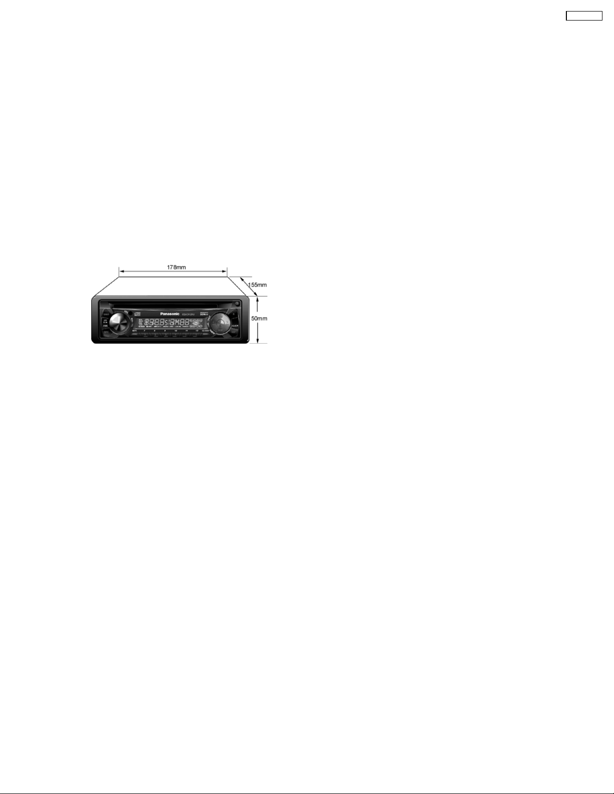
Dimensions** 178×50×155mm
Weight** 1.4kg
* Specifications and the design are subject to possible modification
without notice due to improvements.
** Dimensions and Weight shown are approximate.
© 2004 Matsushita Electric Industrial Co., Ltd. All
rights reserved. Unauthorized copying and
distribution is a violation of law.
CQ-C1101U
CONTENTS
Page Page
1 ABOUT LEAD FREE SOLDER (PbF) 2
2 FEATUERS
3 LASER PRODUCTS
4 REPLACEING THE FUSE
5 MAINTENANCE
6 NOTES
7 DIMENSIONS
8 WIRING CONNECTION
9 BLOCK DIAGRAM
10 TERMINALS DESCRIPTION
11 PACKAGE AND IC BLOCK DIAGRAM 8
2
12 REPLACEM ENT PARTS LIST
13 EXPLODED VIEW (Unit)
2
2
14 CD PLAYER MECHANICAL PARTS LIST
15 EXPLODED VIEW (CD Deck)
3
3
16 PACKING PARTS LIST
3
17 WIRING DIAGRAM
18 SCHEMATIC DIAGRAM-1
4
5
19 SCHEMATIC DIAGRAM-2
20 SCHEMATIC DIAGRAM for printing with Letter size
6
11
16
17
18
19
20
25
27
29
1 ABOUT LEAD FREE
SOLDER (PbF)
Distinction of PbF PCB:
PCBs (manufactured) using lead free solder will have a PbF
stamp on the PCB.
Caution :
· Pb free solder has a higher melting point than standard
solder; Typically the melting point is 50 - 70°F (30 40°C) higher. Please use a soldering iron with
temperature control and adjust it to 700 ± 20°F (370 ±
10°C). In case of using high temperature soldering iron,
please be careful not to heat too long.
· Pb free solder will tend to splash when heated too high
(about 1100°F/600°C)
· This lead free solder will be used for the products after
serial No. 1,000,001.
2 FEATUERS
· Remote Control.
· 18-FM, 6-AM presets with preset scan
· Digital servo for reliable CD playback.
· Removable face plate.
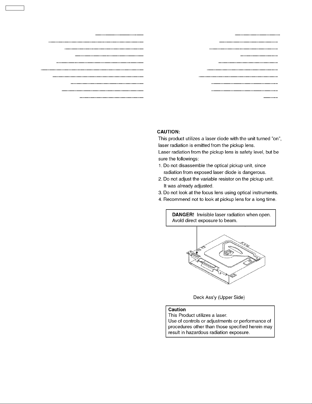
3 LASER PRODUCTS
4 REPLACEING THE FUSE
Use fuses of the same specified rating (15A). Using different
substitutes or fuses with higher ratings, or connecting the
product directly without a fuse, could cause fire or damage to
the stereo unit.
2
5 MAINTENANCE
Your products is designed and manufactured to ensure a
minimum of maintenance. Use a dry, a soft cloth for routine
exterior cleaning. Never use benzine, thinner or other solvents.
6 NOTES
[RADIO BLOCK]
Do not align the AM/FM package block. When the package
block is necessary, it will be supplied already aligned at the
factory.
[CD DECK BLOCK]
This model has no servo alignment points because
microcomputer controls the servo circuit.
7 DIMENSIONS
CQ-C1101U
3
CQ-C1101U
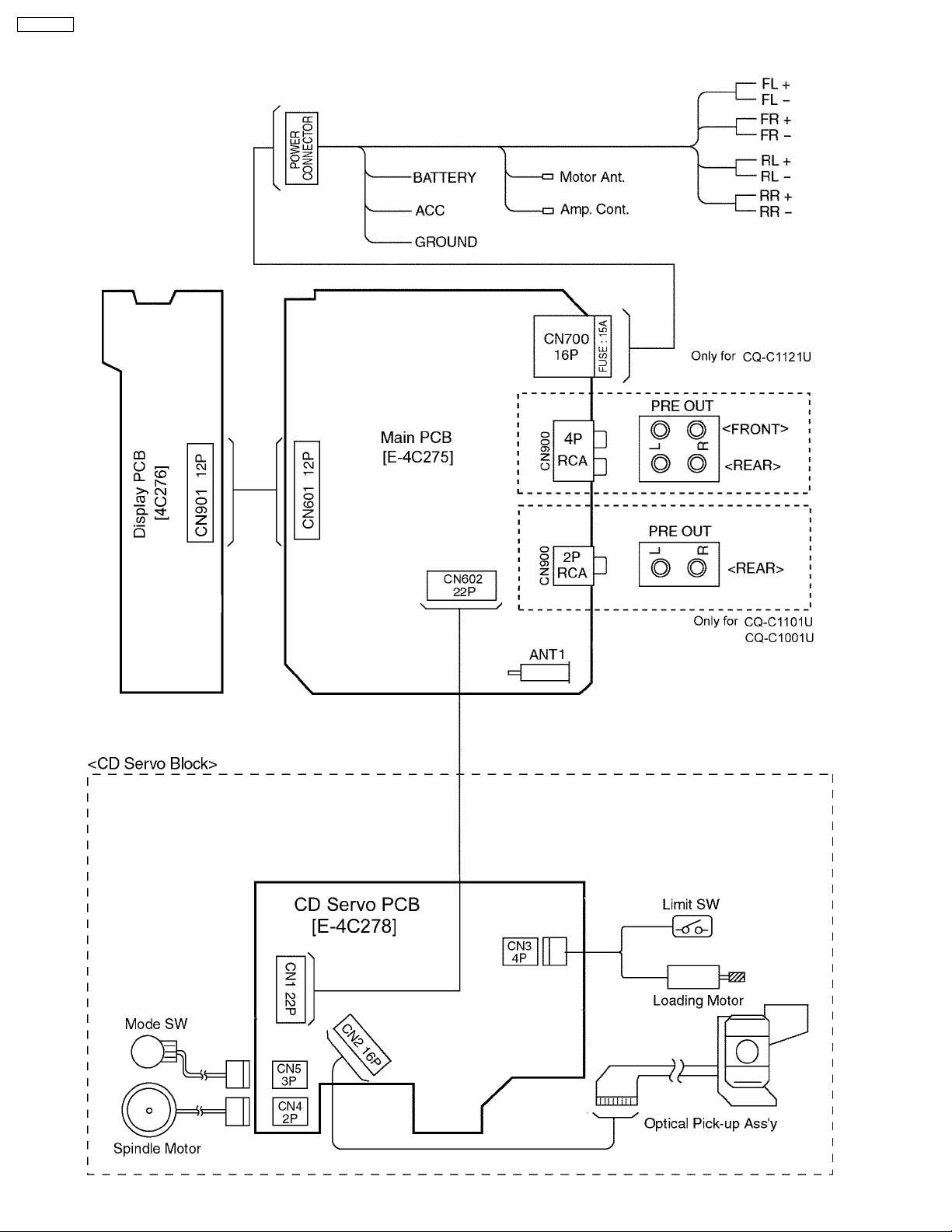
8 WIRING CONNECTION
4
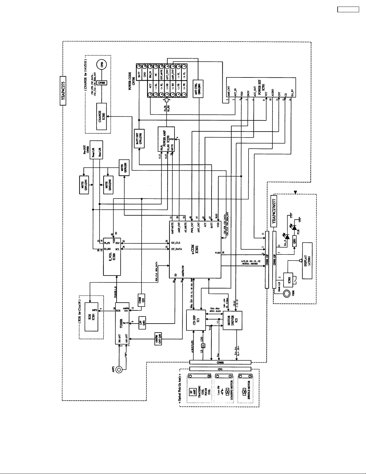
9 BLOCK DIAGRAM
CQ-C1101U
5
CQ-C1101U
10 TERMINALS DESCRIPTION
10.1. Main Block
IC601 : LC7237819C89
Pin
Port Description I/O(V) FM(V) AM(V) CD(V)
No.
1 XIN 4. 5 MHz X’tal and
2 TEST2 GND connection I 0 0 0
3 VREG Bypass condenser
4 VSSCPU GND connection - 0 0 0
5 CDC_DATACD changer data I 0.01 0.01 0.01
6 N.C. None O 0.01 0.01 0
7 CDC_CLK CD changer clock I 0 0.01 0.01
8 CDC_REM
_OUT
9 LCD_DO LCD data output I 5.1 5.17 5.17
10 LCD_DI LCD data input O 4.95 5.01 4.92
11 LCD_CLK LCD clock O 5 5.14 5.12
12 LCD_CE LCD chip enable
13 CD_DO CD data output I 5.3 5.27 4.92
14 CD_DI CD data input O 0.01 0.01 5.12
15 CD_CLK CD clock O 5 5.17 5.1
16 CD_CE CD chip enable O 0.01 0.01 0.4
17 CD_EM CD eject O 0.02 0.02 0.02
18 CD_LM CD loading O 0.01 0.01 5.15
19 CD_S/L CD 24PIN
20 CD_WRQ CD WRQ connection I 5.3 5.29 0.1
21 CD_INSW1CD insert SW input I 0.1 0.1 0.1
22 CD_SW2 CD MECHA SW2 I 5 5.14 5.13
23 CD_LIMI
T_SW
24 CD_DRF CD DRF I 0 0 5.15
25 CD_RST CD reset O 5 5.17 5.14
26 CD_DMUTECD mute O 0 0 0
27 N.C. None O 0 0 0
28 N.C. None O 0 0 5.18
29 PANEL Panel detect I 5.18 5.18 0
30 N.C. GND connection I 0 0 0
31 N.C. GND connection I 0 0 0
32 N.C. GND connection I 0 0 0
33 N.C. None O 0 0 0
34 N.C. None O 0 0 0
35 N.C. None O 0 0 0
36 N.C. None O 0 0 0
37 N.C. None O 0 0 0
38 N.C. None O 0 0 5.14
39 VDDPORT Power supply of
40 VSSPORT GND of PORT - 0 0 0
41 N.C. None O 0 0 0
42 N.C. None O 0 0 0
43 N.C. None O 0 0 0
44 N.C. None O 0 0 0
45 N.C. None O 0 0 0
46 N.C. None O 0 0 0
47 N.C. None O 0 0.02 0.02
48 N.C. None O 0 0 0
49 PWR_CNT Power control O 5 5.15 5.14
50 AMP_CNT Amp stand-by O 5 5.15 5.13
51 AMP_MUTEAmp mute O 5 5.15 5.15
Connection
connected.
CD changer Remote
out
output
connection
CD limit SW I 0 0 5.26
PORT
I 2.4 2.49 2.48
O 2.9 2.99 2.99
O 0.01 0.01 0.01
O 0.1 0.18 0.23
O 0.01 0 0
- 5 5.17 0
Pin
Port Description I/O(V) FM(V) AM(V) CD(V)
No.
56 I2C_CLK Electronic VOL
57 ANT_CNT Motor antena
58 POWER_LEDPower LED O 0.1 0.17 0.17
59 N.C. None O 0.03 0.02 0
60 N.C. (
BZ_OUT
)
61 N.C. None O 0.03 0.02 0
62 N.C. None O 0.03 0.02 0
63 N.C. None O 0.03 0.02 0
64 N.C. None O 0.03 0.02 0
65 N.C. None O 0.03 0.02 0
66 TEL_MUTEExternal MUTE
67 BATT Battery detection I 5.2 5.33 5.33
68 MODE_B ROTARY B input I 0.54 0.62 0.02
69 RDS_CLK RDS clock I 2.65 2.64 2.63
70 REM_IN Remocon data input I 5 5.12 5.11
71 MODE_A ROTARY A input I 0.6 0.59 0.06
72 CDC_STB CD changer strobe
73 NC None O 0.03 0.03 0
74 MONO Compulsion MONO ON O 0.03 0.03 0.03
75 AM_MODE AM change O 8 0.06 8.06
76 FM_MODE FM change O 0.08 8.06 0.08
77 N.C. GND connection I 0.1 0 0
78 INIT_C Initial value C I 0 0 0
79 INIT_B Initial value B I 2.5 5.15 5.14
80 INIT_A Initial value A I 3.23 3.25 3.24
81 VSSADC GND connection - 0 0 0
82 RDS_DATARDS data I 0.3 0.01 2.56
83 ST FM stereo input I 5.3 5.25 0.34
84 SD_FM/AMSignal detection I 3.2 3.51 0.32
85 N.C. GND connection I 0 0 0
86 RESET Reset Input I OFF OFF OFF
87 ACC Power supply I 5.3 5.37 5.42
88 N.C. GND connection I 0 0 0
89 N.C. GND connection I 0 0 0
90 FM/AM_IFCFM/AM IF input I 1.4 1.45 1.45
91 N.C. GND connection I 0.1 0 0
92 SUBPD None O 2 2.09 1.39
93 VDDPLL Power supply of
94 N.C. None I 0 0 0
95 OSC_FM/AMFM/AM osc input I 1.4 1.36 1.43
96 VSSPLL None - 0 0 0
97 N.C. None O 0.3 0.17 0.21
98 EO1 PLL phase
99 TEST1 GND connection I 0 0 0
100 XOUT 4. 5 MHz X’tal and
clock
control
None O 0.03 0.02 0
input
input
PLL
comparison error
output
Connection
O 5 5.17 5.16
O 5 5.17 5.17
I 5.2 5.33 5.33
I 0 0.62 0.06
- 5 5.16 OFF
O 2 2.08 1.38
O 2.5 2.56 2.56
52 N.C. None O 0.03 0.02 0.02
53 SSC Tuner search
54 AF_MUTE AF mute O 5 5.17 5.15
55 I2C_DATAElectronic VOL
sensitivity change
data
O 0.06 0.06 0.06
O 5 5.17 5.16
Note 1 :
Voltage measuerments are with respect to ground, with a
voltmeter (internal resistance : 10M ohms).
6
10.2. Display Block
IC901 : YEAMLC75853NW
Pin No. Port Descriptions I/O
1-35 SEG1-35 LCD segment O 2.5
36-39 NC No connection - 40-43 COM1-4 LCD common O 2.5
44-49 KS1-6 Key data output O 0.9
50-54 KI1-5 Key data input I 0
55 TEST (Connecting to ground) - 0
56 VDD +5V power supply - 5.1
57 VDD1 Ground through capacitor - 3.3
58 VDD2 Ground through capacitor - 1.7
59 Vss Ground - 0
60 OSC CR oscillator - 3.9
61 DO Key data output O 4.4
62 CE Chip enable I 0
63 CLK LCD clock I 0
64 DI LCD data input I 0
(V)
CQ-C1101U
(V)
7
CQ-C1101U
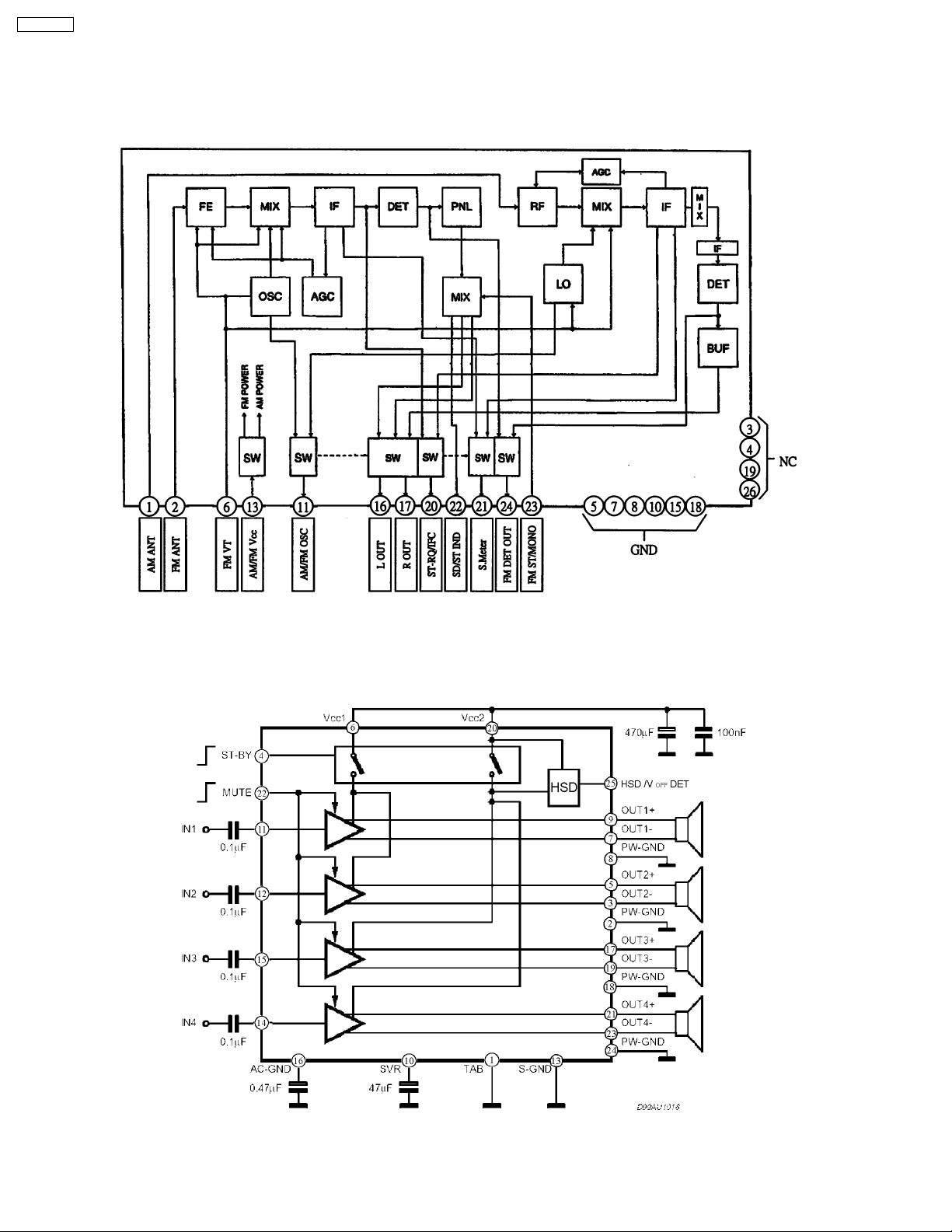
11 PACKAGE AND IC BLOCK DIAGRAM
11.1. Main Block
P50:FAE391-A10
IC270 : C1EA00000041
8
CQ-C1101U
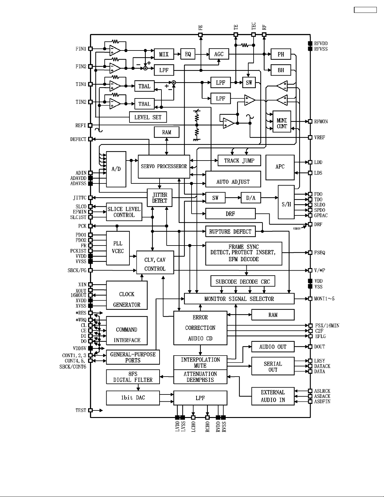
IC1 : LC78646EHUM
9
 Loading...