

Panasonic 2SD1538, 2SD1538A Datasheet
Po wer Transistors
2SD1538, 2SD1538A
Silicon NPN epitaxial planar type
For low-voltage switching
Complementary to 2SB1070 and 2SB1070A
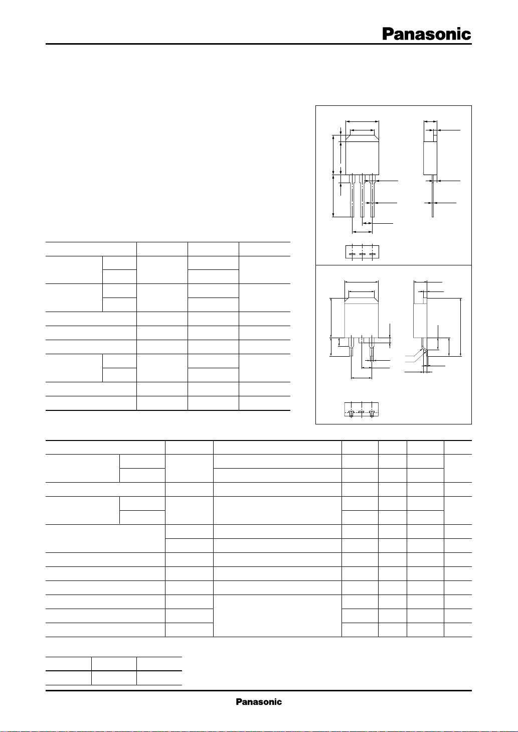
8.5±0.2
6.0±0.5
3.4±0.3
Unit: mm
1.0±0.1
Features
■
●
Low collector to emitter saturation voltage V
●
High-speed switching
●
N type package enabling direct soldering of the radiating fin to
CE(sat)
the printed circuit board, etc. of small electronic equipment.
Absolute Maximum Ratings (T
■
Parameter
Collector to
base voltage
Collector to
emitter voltage
2SD1538
2SD1538A
2SD1538
2SD1538A
Emitter to base voltage
Peak collector current
Collector current
Collector power
dissipation
TC=25°C
Ta=25°C
Junction temperature
Storage temperature
Electrical Characteristics (T
■
Symbol
V
V
V
I
CP
I
C
P
C
T
j
T
stg
Parameter
Collector cutoff
current
2SD1538
2SD1538A
Emitter cutoff current
Collector to emitter
voltage
2SD1538
2SD1538A
Forward current transfer ratio
Collector to emitter saturation voltage
Base to emitter saturation voltage
Transition frequency
Turn-on time
Storage time
Fall time
*
h
Rank classification
FE2
Rank Q P
h
FE2
90 to 180 130 to 260
CBO
CEO
EBO
C
Symbol
I
CBO
I
EBO
V
CEO
h
FE1
*
h
FE2
V
CE(sat)
V
BE(sat)
f
T
t
on
t
stg
t
f
=25˚C)
C
Ratings
40
50
20
40
5
8
4
25
1.3
150
–55 to +150
=25˚C)
VCB = 40V, IE = 0
VCB = 50V, IE = 0
VEB = 5V, IC = 0
IC = 10mA, IB = 0
VCE = 2V, IC = 0.1A
VCE = 2V, IC = 1A
IC = 2A, IB = 0.1A
IC = 2A, IB = 0.1A
VCE = 5V, IC = 0.5A, f = 10MHz
IC = 2A, IB1 = 0.2A, IB2 = – 0.2A,
VCC = 20V
Unit
V
V
V
A
A
W
˚C
˚C
Conditions
10.0±0.310.5min.
10.0±0.3
2.0
4.4±0.5
2.0 1.5±0.1
123
5.08±0.5
213
8.5±0.2
6.0±0.3
5.08±0.5
min
20
40
45
90
1.5max.
0.8±0.1
2.54±0.3
0.8±0.1
2.54±0.3
–0.4
+0
1.5
R0.5
R0.5
1.1 max.
1:Base
2:Collector
3:Emitter
N Type Package (DS)
typ
max
120
0.2
0.5
0.1
1.1max.
0.5max.
1:Base
2:Collector
3:Emitter
N Type Package
Unit: mm
3.4±0.3
1.0±0.1
–0.2
+0.4
3.0
4.4±0.5
0 to 0.4
Unit
50
50
50
µA
µA
V
260
0.5
1.5
V
V
MHz
µs
µs
µs
14.7±0.5
1
Po wer Transistors 2SD1538, 2SD1538A
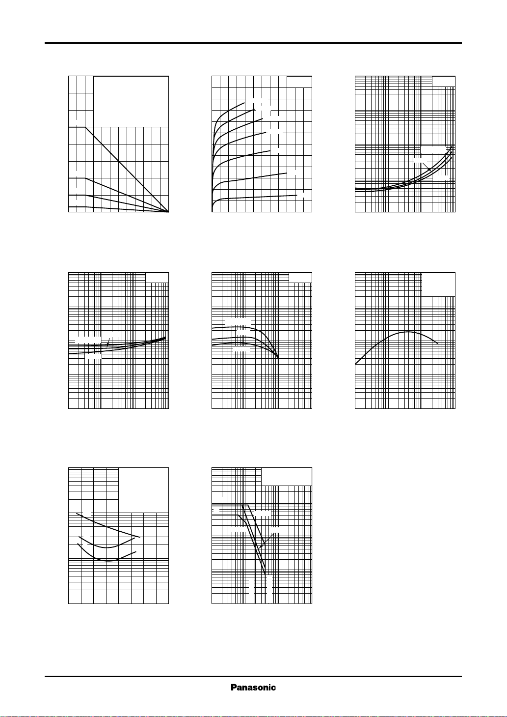
PC—Ta IC—V
40
)
35
W
(
C
30
25
20
15
10
5
Collector power dissipation P
0
0 15012510025 7550
100
)
V
(
30
BE(sat)
10
3
1
0.3
0.1
0.03
Base to emitter saturation voltage V
0.01
0.01 0.1 1 100.03 0.3 3
(1) TC=Ta
(2) With a 100 × 100 × 2mm
Al heat sink
(3) With a 50 × 50 × 2mm
Al heat sink
(4) Without heat sink
(P
(1)
(2)
(3)
(4)
=1.3W)
C
Ambient temperature Ta (˚C
V
BE(sat)—IC
IC/IB=10
TC=–25˚C
25˚C
100˚C
Collector current IC (A
)
CE
6
5
)
A
(
4
C
3
2
IB=60mA
50mA
40mA
30mA
20mA
T
C
10mA
=25˚C
Collector current I
1
0
012108264
)
Collector to emitter voltage VCE (V
hFE—I
10000
3000
FE
1000
TC=100˚C
300
100
30
10
Forward current transfer ratio h
3
1
0.1 1 10 1000.3 3 30
25˚C
–25˚C
Collector current IC (A
5mA
C
VCE=2V
)
)
100
V
(
30
CE(sat)
10
0.3
0.1
0.03
0.01
Collector to emitter saturation voltage V
)
10000
3000
)
MHz
1000
(
T
300
100
30
10
Transition frequency f
V
CE(sat)—IC
3
1
0.01 0.1 1 100.03 0.3 3
TC=100˚C
25˚C
Collector current IC (A
fT—I
C
VCE=5V
f=10MHz
T
C
3
1
0.01 0.1 1 100.03 0.3 3
Collector current IC (A
IC/IB=10
–25˚C
)
=25˚C
)
10
)
3
µs
(
f
,t
1
stg
,t
on
0.3
0.1
Switching time t
0.03
0.01
082647153
Collector current IC (A
2
t
t
t
stg
on
f
ton, t
, tf — I
stg
C
Pulsed tw=1ms
Duty cycle=1%
=10 (IB1=–IB2)
I
C/IB
=20V
V
CC
=25˚C
T
C
Area of safe operation (ASO)
100
30
)
I
CP
10
A
(
I
C
C
3
300ms
1
0.3
0.1
Collector current I
0.03
0.01
1 10 100 10003 30 300
)
Collector to emitter voltage VCE (V
Non repetitive pulse
=25˚C
T
C
t=1ms
10ms
2SD1538
2SD1538A
)
 Loading...