

Panasonic 2SD1535 Datasheet
Po wer Transistors
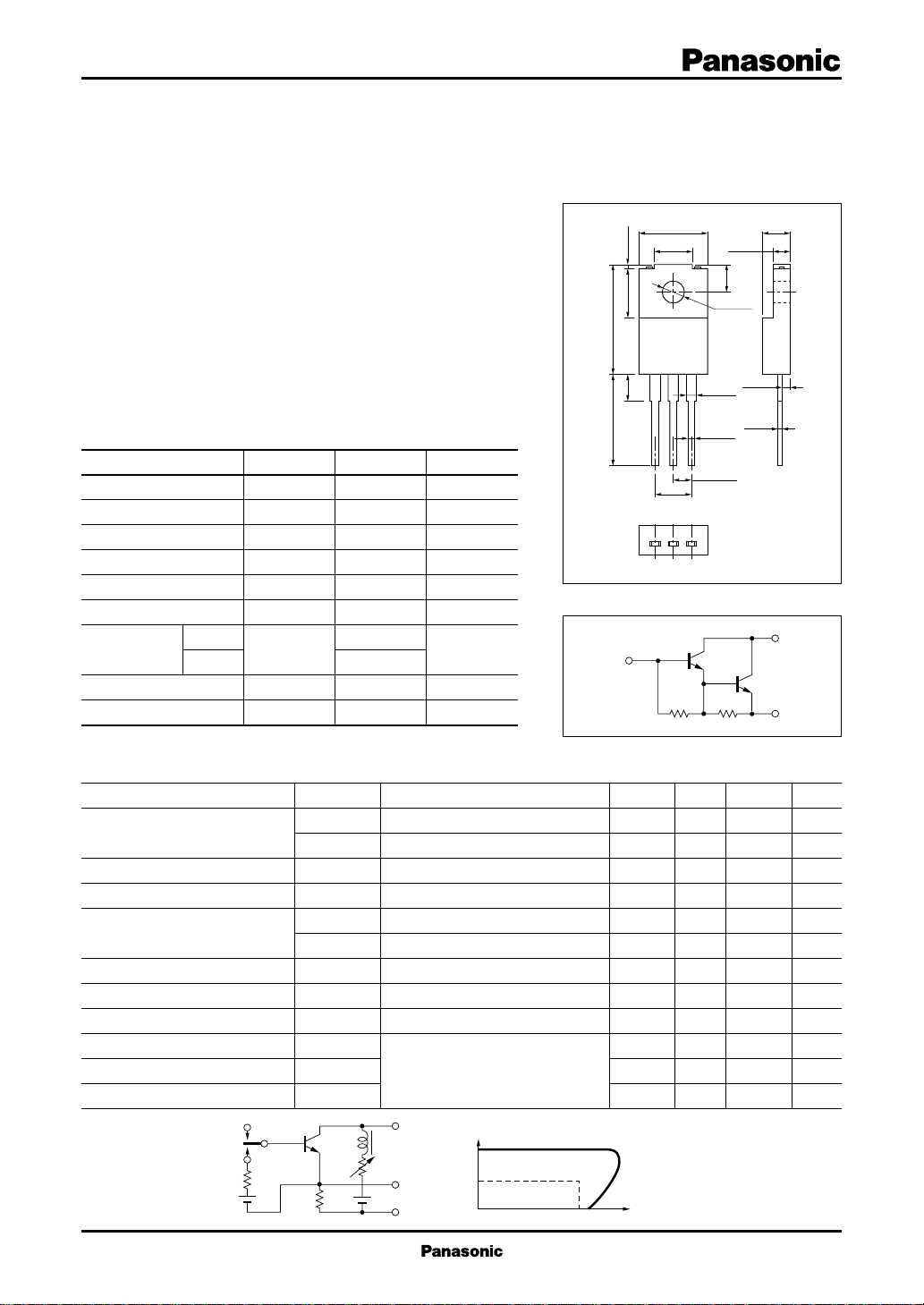
10.0±0.2
5.5±0.2
7.5±0.2
16.7±0.3
0.7±0.1
14.0±0.5
Solder Dip
4.0
0.5
+0.2
–0.1
1.4±0.1
1.3±0.2
0.8±0.1
2.54±0.25
5.08±0.5
213
2.7±0.2
4.2±0.2
4.2±0.2
φ3.1±0.1
2SD1535
Silicon NPN triple diffusion planar type Darlington
For high power amplification
Features
■
●
Extremely satisfactory linearity of the forward current transfer
ratio h
●
●
●
■
Collector to base voltage
Collector to emitter voltage
Emitter to base voltage
Peak collector current
Collector current
Base current
Collector power
dissipation
Junction temperature
Storage temperature
FE
High collector to base voltage V
CBO
Wide area of safe operation (ASO)
Full-pack package which can be installed to the heat sink with
one screw
Absolute Maximum Ratings (T
Parameter
TC=25°C
Ta=25°C
Symbol
V
CBO
V
CEO
V
EBO
I
CP
I
C
I
B
P
C
T
j
T
stg
=25˚C)
C
Ratings
500
400
12
14
7
0.5
50
2
150
–55 to +150
Unit
V
V
V
A
A
A
W
˚C
˚C
Unit: mm
1:Base
2:Collector
3:Emitter
TO–220 Full Pack Package(a)
Internal Connection
C
B
E
Electrical Characteristics (T
■
Parameter
Collector cutoff current
Emitter cutoff current
Collector to emitter voltage
Forward current transfer ratio
Collector to emitter saturation voltage
Base to emitter saturation voltage
Transition frequency
Turn-on time
Storage time
Fall time
*
V
CEO(sus)
T est circuit
60Hz
120Ω
6V
Symbol
I
CBO
I
CEO
I
EBO
V
CEO(sus)
h
FE1
h
FE2
V
CE(sat)
V
BE(sat)
f
T
t
on
t
stg
t
f
1Ω
=25˚C)
C
Conditions
VCB = 500V, IE = 0
VCE = 400V, IB = 0
VEB = 12V, IC = 0
*
IC = 100mA, RBZ = ∞, L = 25mH
VCE = 2V, IC = 2A
VCE = 2V, IC = 6A
IC = 7A, IB = 70mA
IC = 7A, IB = 70mA
VCE = 10V, IC = 0.5A, f = 1MHz
IC = 7A, IB1 = 70mA, IB2 = –70mA,
VCC = 300V
X
L 25mH
15V
IC(A)
0.2
Y
G
0.1
min
400
typ
max
0.1
0.1
100
Unit
mA
mA
mA
mA
500
200
2.0
2.5
20
1.5
5.0
6.5
(V)
V
80
CE
V
V
MHz
µs
µs
µs
1
Po wer Transistors 2SD1535
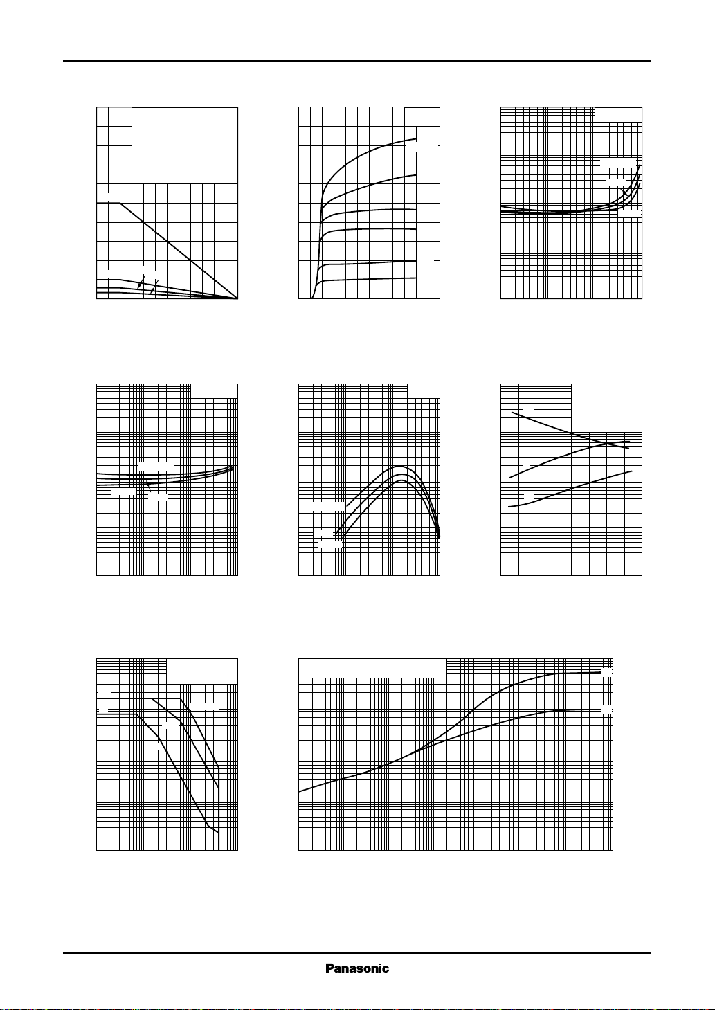
PC—Ta IC—V
100
)
W
(
80
C
60
40
20
Collector power dissipation P
0
0 15012510025 7550
100
)
V
(
30
BE(sat)
10
3
1
0.3
0.1
0.03
Base to emitter saturation voltage V
0.01
0.01 0.1 1 100.03 0.3 3
(1) TC=Ta
(2) With a 100 × 100 × 2mm
Al heat sink
(3) With a 50 × 50 × 2mm
Al heat sink
(4) Without heat sink
(P
=2.0W)
C
(1)
(3)
(2)
(4)
Ambient temperature Ta (˚C
V
BE(sat)—IC
IC/IB=100
TC=–25˚C
100˚C
25˚C
Collector current IC (A
)
CE
10
8
)
A
(
C
6
4
Collector current I
2
0
0654132
)
Collector to emitter voltage VCE (V
hFE—I
100000
30000
FE
10000
3000
1000
300
TC=100˚C
100
25˚C
Forward current transfer ratio h
–25˚C
30
10
0.01 0.1 1 100.03 0.3 3
Collector current IC (A
TC=25˚C
IB=20mA
10mA
5mA
3mA
2mA
1mA
C
VCE=2V
)
)
100
V
(
30
CE(sat)
10
0.3
0.1
0.03
0.01
Collector to emitter saturation voltage V
)
100
30
)
µs
(
10
f
,t
stg
,t
on
0.3
0.1
Switching time t
0.03
0.01
V
CE(sat)—IC
IC/IB=100
TC=100˚C
3
1
0.01 0.1 1 100.03 0.3 3
25˚C
Collector current IC (A
ton, t
, tf—I
t
stg
3
t
f
1
t
on
082647153
stg
C
Pulsed tw=1ms
Duty cycle=1%
I
=100 (IB1=–IB2)
C/IB
=300V
V
CC
T
=25˚C
C
Collector current IC (A
–25˚C
)
)
Area of safe operation (ASO) R
100
30
I
CP
)
I
10
A
C
(
C
3
1
0.3
0.1
Collector current I
0.03
0.01
1 10 100 10003 30 300
Non repetitive pulse
=25˚C
T
C
1ms
DC
t=0.1ms
Collector to emitter voltage VCE (V
)
2
10
(1) Without heat sink
(2) With a 100 × 100 × 2mm Al heat sink
)
˚C/W
(
10
(t)
th
1
–1
10
Thermal resistance R
–2
10
–3
10
–2
10
2
—t
th(t)
(1)
(2)
–1
110
Time t (s
10 10
)
2
10
3
4
10
 Loading...