

Panasonic 2SD1511 Datasheet
Transistor
2SD1511
Silicon NPN epitaxial planer type darlington
For low-frequency output amplification
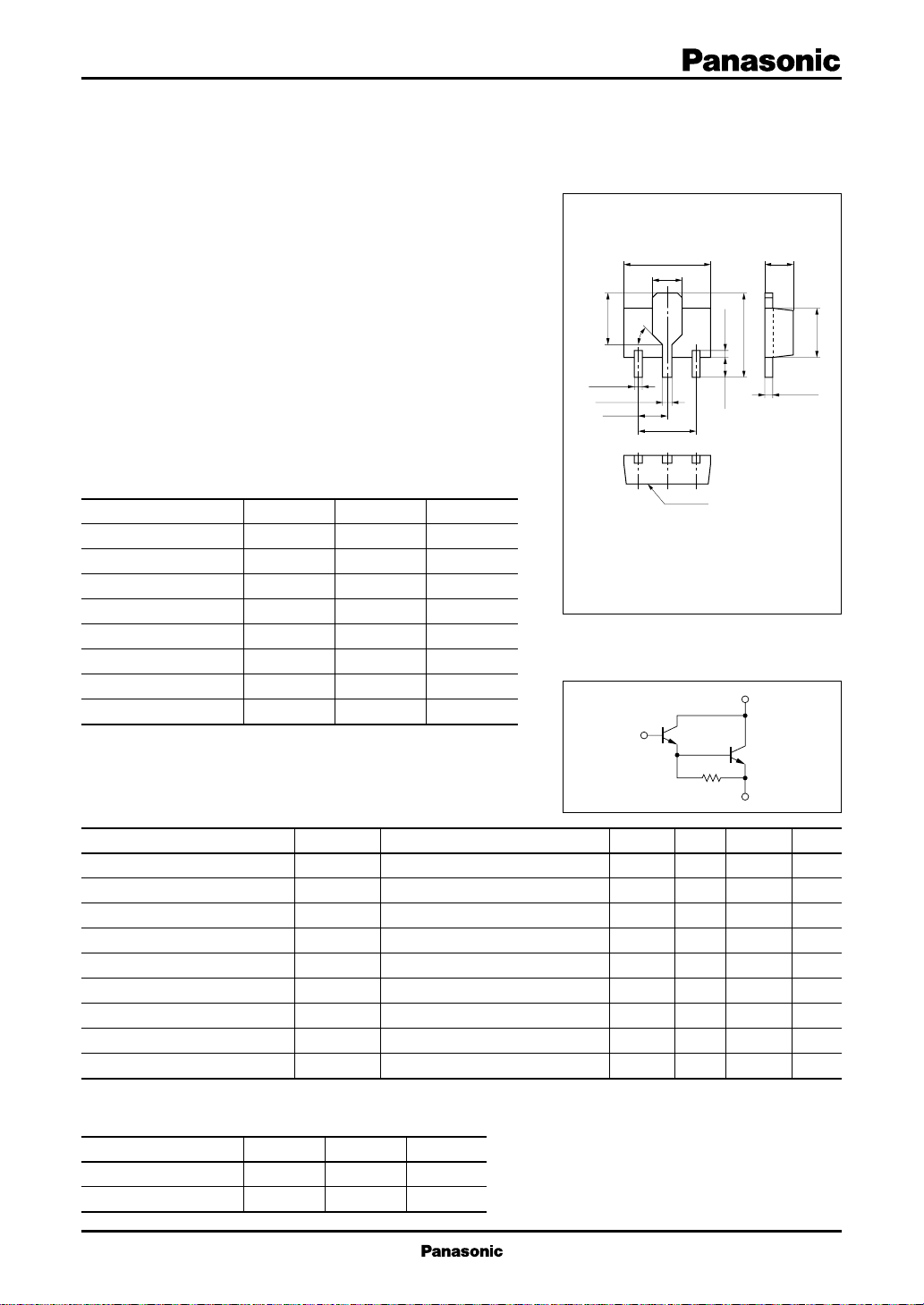
Unit: mm
Features
■
●
Forward current transfer ratio hFE is designed high, which is appropriate to the driver circuit of motors and printer bammer: h
= 4000 to 2000.
●
A shunt resistor is omitted from the driver.
●
Mini Power type package, allowing do wnsizing of the equipment
and automatic insertion through the tape packing and the magazine packing.
Absolute Maximum Ratings (Ta=25˚C)
■
Parameter
Collector to base voltage
Collector to emitter voltage
Emitter to base voltage
Peak collector current
Collector current
Collector power dissipation
Junction temperature
Storage temperature
*
Printed circuit board: Copper foil area of 1cm2 or more, and the board
thickness of 1.7mm for the collector portion
Symbol
V
CBO
V
CEO
V
EBO
I
CP
I
C
*
P
C
T
j
T
stg
Ratings
100
80
5
1.5
1
1
150
–55 ~ +150
Unit
V
V
V
A
A
W
˚C
˚C
4.5±0.1
1.6±0.2
FE
2.6±0.1
45°
0.4±0.08
0.5±0.08
1.5±0.1
3.0±0.15
321
marking
1:Base
2:Collector EIAJ:SC–62
3:Emitter Mini Power Type Package
1.5±0.1
–0.20
+0.25
0.4max.1.0
4.0
–0.2
+0.1
2.5±0.1
0.4±0.04
Marking symbol : P
Internal Connection
C
B
Electrical Characteristics (Ta=25˚C)
■
Parameter
Collector cutoff current
Emitter cutoff current
Collector to base voltage
Collector to emitter voltage
Emitter to base voltage
Forward current transfer ratio
Collector to emitter saturation voltage
Base to emitter saturation voltage
Transition frequency
*1
hFE Rank classification
Symbol
I
CBO
I
EBO
V
CBO
V
CEO
V
EBO
*1
h
FE
V
CE(sat)
V
BE(sat)
f
T
Rank Q R S
h
FE
4000 ~ 10000 8000 ~ 20000 16000 ~ 40000
Marking Symbol PQ PR PS
Conditions
VCB = 25V, IE = 0
VEB = 4V, IC = 0
IC = 100µA, IE = 0
IC = 1mA, IB = 0
IE = 100µA, IC = 0
VCE = 10V, IC = 1A
IC = 1.0A, IB = 1.0mA
IC = 1.0A, IB = 1.0mA
*2
*2
*2
VCB = 10V, IE = –50mA, f = 200MHz
min
100
80
5
4000
E
typ
max
100
100
40000
1.8
2.2
150
*2
Pulse measurement
Unit
nA
nA
V
V
V
V
V
MHz
1
Transistor
2SD1511
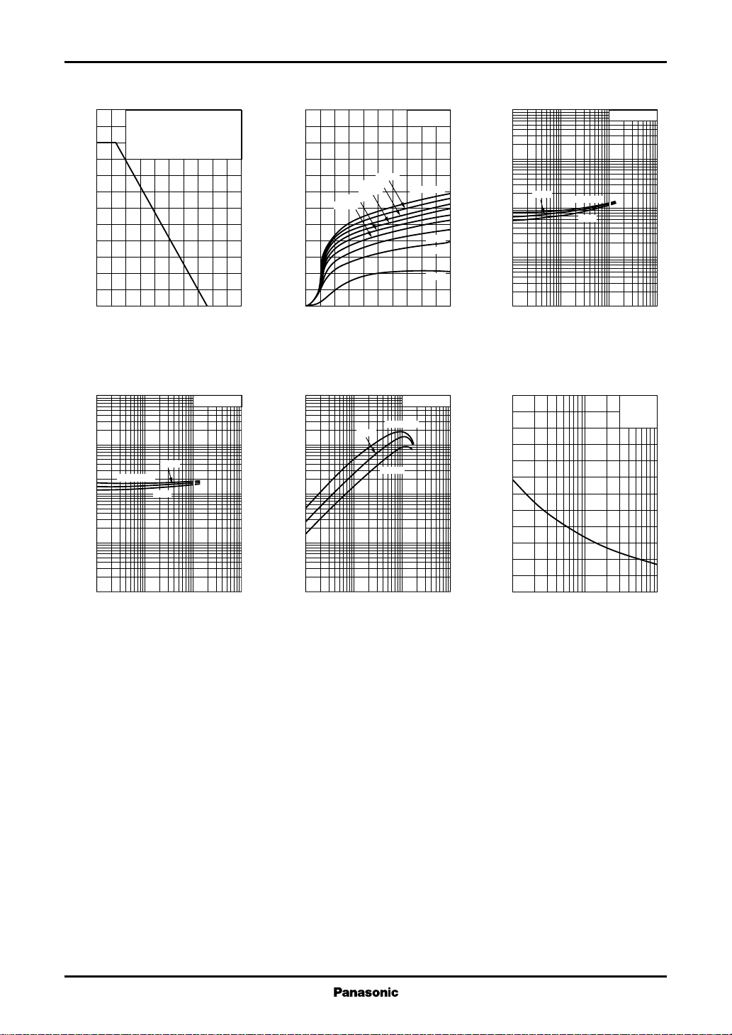
PC — Ta IC — V
1.2
)
W
(
1.0
C
0.8
0.6
0.4
0.2
Collector power dissipation P
100
)
V
(
30
BE(sat)
10
Printed circut board: Copper
foil area of 1cm
the board thickness of 1.7mm
for the collector portion.
0
0 20016040 12080
2
or more, and
Ambient temperature Ta (˚C
V
— I
BE(sat)
3
Ta=–25˚C
1
25˚C
75˚C
C
IC/IB=1000
V
CE
2.4
2.0
)
A
(
1.6
C
1.2
0.8
100µA
120µA
160µA
140µA
Collector current I
0.4
0
0108264
)
Collector to emitter voltage VCE (V
hFE — I
5
10
FE
4
10
3
10
25˚C
Ta=25˚C
180µA
IB=200µA
80µA
60µA
40µA
C
VCE=10V
Ta=75˚C
–25˚C
)
100
V
(
30
CE(sat)
10
3
25˚C
1
0.3
0.1
0.03
0.01
Collector to emitter saturation voltage V
0.01 0.1 1 100.03 0.3 3
)
Collector current IC (A
30
)
pF
(
25
ob
20
15
— I
CE(sat)
Ta=–25˚C
75˚C
Cob — V
CB
C
IC/IB=1000
)
IE=0
f=1MHz
Ta=25˚C
0.3
0.1
0.03
Base to emitter saturation voltage V
0.01
0.01 0.1 1 100.03 0.3 3
Collector current IC (A
)
2
10
Forward current transfer ratio h
10
0.01 0.1 1 100.03 0.3 3
Collector current IC (A
10
5
Collector output capacitance C
0
1 3 10 30 100
)
Collector to base voltage VCB (V
)
2
 Loading...