

ON Semiconductor NCP81246 Datasheet
NCP81246
l
Three-Rail Controller
with Intel Proprietary
Interface for IMVP8 CPU
Applications
The NCP81246 contains a two-phase, and two single-phase buck
regulators optimized for Intel IMVP8 compatible CPUs.
The two-phase controller combines true differential voltage sensing,
differential inductor DCR current sensing, input voltage feed-forward,
and adaptive voltage positioning to provide accurately regulated
power for IMVP8 Rail2.
The two single-phase controllers can be used for Rail1, Rail3 and
Rail4 rails. Both make use of ON Semiconductor’s patented enhanced
RPM operation. RPM control maximizes transient response while
allowing for smooth transitions between discontinuous frequency
scaling operation and continuous mode full power operation. The
single-phase rails have an ultralow offset current monitor amplifier
with programmable offset compensation for ultra high accuracy
current monitoring.
The NCP81246 offers three internal MOSFET drivers with a single
external PWM signal.
Two-Phase Rail Features
• Dual Edge Modulation for Fastest Initial Response to Transient
Loading
• High Performance Operational Error Amplifier
• Digital Soft Start Ramp
• Dynamic Reference Injection
• Accurate Total Summing Current Amplifier(Patent #US6683441)
• Dual High Impedance Differential Voltage and Total Current Sense
Amplifiers
• Phase-to-Phase Dynamic Current Balancing
• True Differential Current Balancing Sense Amplifiers for Each Phase
• Adaptive Voltage Positioning (AVP)
• Switching Frequency Range of 300 kHz – 750 kHz
• Vin range 4.5 V to 25 V
• Start-Up into Pre-Charged Loads While Avoiding False OVP
• UltraSonic Operation
• These Devices are Pb−Free, Halogen Free/BFR Free and are RoHS
Compliant
(Patent #US7057381)
onsemi.com
www.
521
QFN52
MN SUFFIX
CASE 485BE
MARKING DIAGRAM
NCP81246
FAWLYYWW
G
NCP81246 = Specific Device Code
F = Wafer Fab
A = Assembly Site
WL = Lot ID
YY = Year
WW = Work Week
G = Pb-Free Package
ORDERING INFORMATION
Device Package Shipping
NCP81246MNTXG QFN52
(Pb−Free)
†For information on tape and reel specifications,
including part orientation and tape sizes, please
refer to our Tape and Reel Packaging Specification
Brochure, BRD8011/D.
5000 / Tape & Ree
†
Single-Phase Rail Features
• Enhanced RPM Control System
• Ultra Low Offset IOUT Monitor
• Dynamic VID Feed-Forward
• Programmable Droop Gain
• Zero Droop Capable
Semiconductor Components Industries, LLC, 2017
February, 2018 − Rev. 6
• Thermal Monitor
• UltraSonic Operation
• Adjustable Vboot
• Digitally Controlled Operating Frequency
1 Publication Order Number:
NCP81246/D
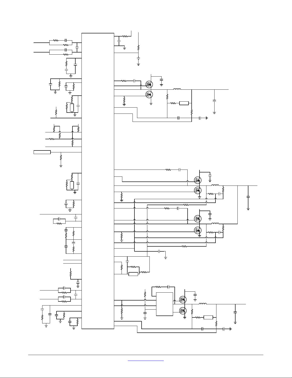
SKT_SNS+
SKT_SNS*
Batt chrgr
NCP81246
+5 V
+5 V
VCC
VSP
VSN
COMP
ILIM
IOUT
TSENSE
V
PU
NTC
V
PU
VRHOT
V
PU
SDIO
ALERT
SCLK
PSYS
GND
PVCC
BST
HG
SW
CSP
CSN
LG
V
IN
VCC_Rail1
NTC
SKT_SNS+
SKT_SNS*
SKT_SNS+
SKT_SNS*
V
TSENSE
BST
HG
NCP81246
NTC
IOUT
VSP
VSN
DIFFOUT
FB
COMP
EN
V
VRRDY
IN
VRMP
VSP
VSN
COMP
IOUT
ILIM
SW
CSP1
BST
HG
SW
CSP2
CSREF
CSSUM
ILIM
CSCOMP
PWM
DRON
CSP
CSN
LG
LG
NTC
VRDV
BST
PWM
HG
SW
EN
VCC
LG
NCP81253
V
IN
IN
VCC_Rail2
V
IN
VCC_Rail3
NTC
Figure 1. Application Schematic
www.onsemi.com
2
NCP81246
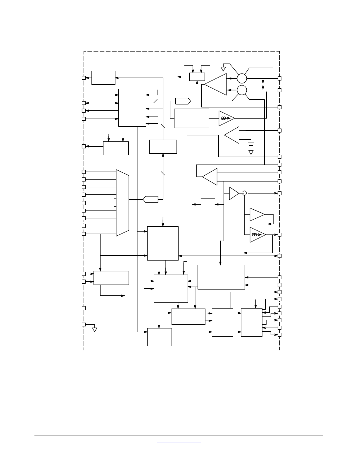
VR_HOT#
SDIO
ALERT#
SCLK
VR_RDY
ROSC
ICCMAX_2PH
ICCMAX_1A
ICCMAX_1B
ADDR_VBOOT
TSENSE_2PH
TSENSE_1A
PSYS/TSENSE_1B
VRAMP
Thermal
Monitor
ENABLE
ENABLE
(VSP−VSN)
IOUT_2ph
IOUT_1a
IOUT_1b
VR Ready
Logic
Intel pro-
prietary
interface
Interface
& Logic
MUX
DRVON
PS#
ADC
OCP
OVP
Data
Registers
ENABLE
PS#
Oscillator
& RAMP
Generators
VRMP
VSP VSN
OVP
OVP
DAC
DAC
Feed-Forward
Current
Sense
OVP
AMP
MAX
OVP
DRVON
DIFF
AMP
−
+
+
−
DAC
Error
AMP
1.3 V
1.3 V
Buffer
IOUT
S
VSP
VSN
S
CSCOMP
−
+
Over-Current
Programming
Over-Current
Comparators
CSREF
VSP_2PH
VSN_2PH
DIFFOUT_2PH
FB_2PH
COMP_2PH
CSCOMP_2PH
CSSUM_2PH
CSREF_2PH
ILIM_2PH
OCP
IOUT_2PH
Current
Monitor
DRVON
VCC
EN
PVCC
GND
UVLO&EN
Comparators
ENABLE
OVP
OCP
PS#
PWM
Generators
PVM2
PS#
Power
State
Gate
COMP
PVM1
Zero Current
Detection
Current Balance
Amplifiers
IPH2
IPH1
ADDR_VBOOT
Config
Figure 2. 2-Phase Rail Block Diagram
PVCC
Gate
Drivers
CSP2_2PH
CSP1_2PH
PWM
HG1
SW1
LG1
HG2
SW2
LG2
www.onsemi.com
3
NCP81246
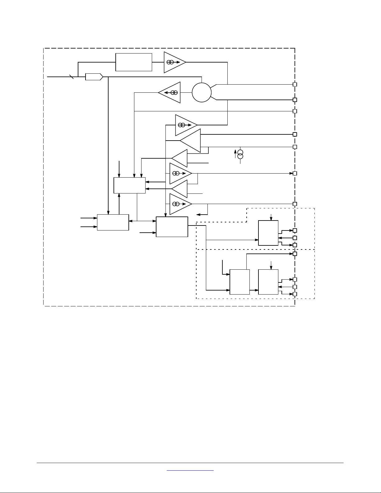
A
B
From Intel
proprietary
interface
Interface
VRMP
FREQ
DAC
DAC
Generator
DRVON
RAMP
DAC
Feed-Forward
COMP
PWM
Generator
RAMP
PWM
PS#
OVP
CURR
OCP
gm
Zero
Current
Detection
DAC Feed-Forward Current
DAC
OVP
OCP
+
AV = 1
OVP REF
OCP REF
IOUT
VSN
+
S
VSP
−
Droop
Current
+
Current
−
Sense AMP
Over-Current Programming
Over-Current
Comparators
Current
Monitor
ADDR_VBOOT
Config
Offset
Adjust
Gate
Driver
PVCC
Gate
Driver
PVCC
VSN_1x
VSP_1x
COMP_1x
CSP_1x
CSN_1x
ILIM_1x
IOUT_1x
HG3
SW3
LG3
PWM
HG2
SW2
LG2
1-Phase
Only
1-Phase
Only
Figure 3. Single-Phase Block Diagram
www.onsemi.com
4
IOUT_2ph
DIFFOUT_2ph/ICCMAX_2ph
FB_2ph
COMP_2ph
ILIM_2ph
CSCOMP_2ph
CSSUM_2ph
CSREF_2ph
CSP2_2ph
CSP1_2ph
TSENSE_2ph
VRMP
VCC
NCP81246
VSN_2ph
VSP_2ph
PSYS
VSP_1b
VSN_1b
COMP_1b
ILIM_1b
CSN_1b
CSP_1b
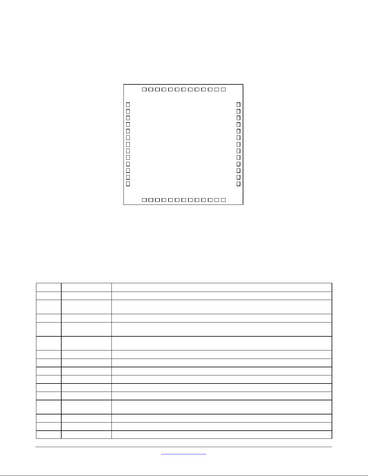
52515049484746454443424140
1
2
3
4
5
6
7
8
9
10
11
12
13
NCP81246
TAB: GROUND
(Not to Scale)
IOUT_1b
VR_RDYENPWM/ADDR_VBOOT
39
DRON
38
SCLK
37
ALERT#
36
SDIO
35
VR_HOT#
34
IOUT_1a
33
CSP_1a
32
CSN_1a
31
ILIM_1a
30
COMP_1a
29
VSN_1a
28
VSP_1a
27
TSENSE_1a
14151617181920212223242526
HG1
BST1
SW1
LG1/ROSC
PVCC
HG2
SW2
BST2
LG2/ICCMAX_1a
LG3/ICCMAX_1b
SW3
HG3
BST3
Figure 4. Pin Configuration
Table 1. NCP81246 PIN DESCRIPTIONS
Pin No.
1 IOUT_2ph A resistor to ground programs IOUT gain for the two-phase regulator.
2 DIFFOUT_2ph/
3 FB_2ph Error amplifier voltage feedback for two-phase regulator.
4 COMP_2ph Output of the error amplifier and the inverting inputs of the PWM comparators for two-phase
5 ILIM_2ph Over-current threshold setting − programmed with a resistor to CSCOMP_2ph for two-phase
6 CSCOMP_2ph Output of total-current-sense amplifier for two-phase regulator.
7 CSSUM_2ph Inverting input of total-current-sense amplifier for two-phase regulator.
8 CSREF_2ph Total-current-sense amplifier reference voltage input for two-phase regulator.
9 CSP2_2ph Non-inverting input to current-balance amplifier for Phase 2 of the two-phase regulator.
10 CSP1_2ph Non-inverting input to current-balance amplifier for Phase 1 of the two-phase regulator.
11 TSENSE_2ph Temperature sense input for the two-phase regulator.
12 VRMP Feed-forward input of Vin for the ramp-slope compensation. The current fed into this pin is used to
13 VCC Power for the internal control circuits. A decoupling capacitor is connected from this pin to ground.
14 BST1 High-side bootstrap supply for Phase 1 of the two-phase regulator.
15 HG1 High-side FET gate driver output for Phase 1 of the two-phase regulator.
Symbol Description
ICCMAX_2ph
Output of the two-phase regulator’s differential remote sense amplifier.
During start-up, the two-phase regulator’s ICCMAX is programmed with a pull-down on this pin.
regulator.
regulator.
control the ramp of the PWM slopes.
www.onsemi.com
5

NCP81246
Table 1. NCP81246 PIN DESCRIPTIONS (continued)
Pin No. DescriptionSymbol
16 SW1 Current return for high-side FET gate driver for Phase 1 of the two-phase regulator.
17 LG1/ROSC Low-side FET gate driver output for Phase 1 of the two-phase regulator.
18 PVCC Power supply for all three internal FET gate drivers.
19 LG2/ICCMAX_1a Low-side FET gate driver output for Phase 2 of the two-phase regulator, or output of single-phase
20 SW2 Current return for high-side FET gate driver for Phase 2 of the two-phase regulator, or for
21 HG2 High-side FET gate driver output for Phase 2 of the two-phase regulator, or for single-phase
22 BST2 High-side bootstrap supply for Phase 2 of the two-phase regulator, or for single-phase regulator 1b.
23 LG3/ICCMAX_1b Low-side FET gate driver output for single-phase regulator 1a.
24 SW3 Current return for high-side FET gate driver for single-phase regulator 1a.
25 HG3 High-side FET gate driver output for single-phase regulator 1a.
26 BST3 High-side bootstrap supply for single-phase regulator 1a.
27 TSENSE_1a Temperature sense input for the single-phase regulators.
28 VSP_1a Differential Output Voltage Sense Positive for single-phase regulator 1a.
29 VSN_1a Differential Output Voltage Sense Negative for single-phase regulator 1a.
30 COMP_1a Compensation for single-phase regulator 1a.
31 ILIM_1a A resistor to ground programs the current-limit for single-phase regulator 1a.
32 CSN_1a Differential current sense negative for single-phase regulator 1a.
33 CSP_1a Differential current sense positive for single-phase regulator 1a.
34 IOUT_1a A resistor to ground programs IOUT gain for single-phase regulator 1a.
35 VR_HOT# Thermal logic output for over temperature.
36 SDIO Serial VID data interface
37 ALERT# Serial VID ALERT#
38 SCLK Serial VID clock
39 DRON Bi-directional FET driver enable
40 PWM/
ADDR_VBOOT
41 EN Enable. High enables all three rails.
42 VR_RDY VR_RDY indicates all three rails are ready to accept Intel proprietary interface commands.
43 IOUT_1b A resistor to ground programs IOUT gain for single-phase regulator 1b.
44 CSP_1b Differential current sense positive for single-phase regulator 1b.
45 CSN_1b Differential current sense negative for single-phase regulator 1b.
46 ILIM_1b A resistor to ground programs the current-limit for single-phase regulator 1b.
47 COMP_1b Compensation for single-phase regulator 1b.
48 VSN_1b Differential Output Voltage Sense Negative for single-phase regulator 1b.
49 VSP_1b Differential Output Voltage Sense Positive for single-phase regulator 1b.
50 PSYS/TSENSE_1b System power signal input. Resistor to ground for scaling /
51 VSP_2ph Differential Output Voltage Sense Positive for the two-phase regulator.
52 VSN−2ph Differential Output Voltage Sense Negative for the two-phase regulator.
During start-up ROSC is programmed with a pull-down resistor on this line.
regulator 1b.
During start-up, regulator 1a’s ICCMAX is programmed with a pull-down on this pin.
single-phase regulator 1b.
regulator 1b.
During start-up, regulator 1b
PWM output for phase 2 of the two-phase regulator or single-phase regulator 1b.
During start-up, a resistor to ground programs Intel proprietary interface address and VBOOT
options for all three rails.
Temperature sense input for the single-phase regulators.
s ICCMAX is programmed with a pull-down on this pin.
www.onsemi.com
6
NCP81246
Table 2. ABSOLUTE MAXIMUM RATINGS
Pin Symbol
COMP_2ph VCC + 0.3 V −0.3 V 2mA 2mA
CSCOMP_2ph VCC + 0.3 V −0.3 V 2mA 2mA
VSN_2ph GND + 0.3 V GND – 0.3 V 1mA 1mA
DIFFOUT_2ph /
IccMax_2ph
VCC 6.5 V −0.3 V 100 mA 100 mA
PVCC 6.5 V −0.3 V 100 mA 100 mA
VRMP 25 V −0.3 V 100 mA 100 mA
SW_x 35 V
BST_x 35 V wrt / GND
40 V ≤ 50 ns wrt / GND
LG_x / ICCMAX_x VCC + 0.3 V −0.3 V
HG_x BST + 0.3 V −0.3 V wrt / SW
All Other Pins VCC + 0.3 V −0.3 V 100 mA 100 mA
Stresses exceeding those listed in the Maximum Ratings table may damage the device. If any of these limits are exceeded, device functionality
should not be assumed, damage may occur and reliability may be affected.
*All signals referenced to GND unless noted otherwise.
V
MAX
V
MIN
I
SOURCE
I
SINK
VCC + 0.3 V −0.3 V 2mA 2mA
−5 V 100 mA 100 mA
40 V ≤ 50 ns
−0.3 V wrt / SW 100 mA 100 mA
6.5 V wrt / SW
100 mA 100 mA
−2 V ≤ 200 ns
100 mA 100 mA
−2 V ≤ 200 ns wrt /SW
Table 3. THERMAL INFORMATION
Description
Thermal Characteristic QFN Package (Note 1)
Operating Junction Temperature Range (Note 2) T
Operating Ambient Temperature Range −40 to +100
Maximum Storage Temperature Range T
Moisture Sensitivity Level QFN Package MSL 1
*The maximum package power dissipation must be observed.
1. JESD 51−5 (1S2P Direct-Attach Method) with 0 LFM
2. JESD 51−7 (1S2P Direct-Attach Method) with 0 LFM
Symbol Value Unit
R
q
JA
J
68
−40 to +125
_C/W
_C
_C
STG
− 40 to +150
_C
Table 4. ELECTRICAL CHARACTERISTICS − GENERAL
(Unless otherwise stated: −40°C<TA< 100°C; 4.75 V < VCC< 5.25 V; C
Parameter
Test Conditions Min Typ Max Unit
BIAS SUPPLY
VCC Voltage Range
VCC Quiescent Current
4.75 − 5.25 V
EN = High − 26 − mA
EN = Low − 20 −
VCC UVLO
VCC Rising − − 4.5 V
VCC Falling 4 − − V
PVCC Voltage Range 4.75 − 5.25 V
PVCC Quiescent Current
EN = Low (Shutdown) − − 1
EN = High, No Switching − − 1.5 mA
VRAMP Voltage Range 5 − 20 V
VRAMP UVLO
VRAMP Rising − − 4.25 V
VRAMP Falling 3 − − V
ENABLE INPUT
Upper Threshold 0.8 − − V
VCC
= 0.1 mF)
mA
mA
www.onsemi.com
7
NCP81246
Table 4. ELECTRICAL CHARACTERISTICS − GENERAL (continued)
(Unless otherwise stated: −40°C<TA< 100°C; 4.75 V < VCC < 5.25 V; C
Parameter UnitMaxTypMinTest Conditions
ENABLE INPUT
Lower Threshold
Enable Delay Time − − 2.5 ms
Enable High Input Leakage Current − − 0.5
PHASE DETECTION
CSP Pin Threshold Voltage
Phase Detect Timer − 1.75 − ms
DAC SLEW RATE
Soft Start Slew Rate
Slew Rate Slow − 15 −
Slew Rate Fast − 30 −
DRVON
Output High Voltage 3 − − V
Output Low Voltage − − 0.1 V
Rise Time
Fall Time − 2.5 − ns
Internal Pull-Down Resistance EN = Low − 69.5 −
T
SENSE
Bias Current −40°C to 100°C 115 120 125
Alert# Assert Threshold − 485 − mV
Alert# De-Assert Threshold − 513 − mV
VR_Hot Assert Threshold − 466 − mV
VR_Hot De-Assert Threshold − 490 − mV
VR_Rdy OUTPUT
Output Low Saturation Voltage
Output Leakage Current When High VR_RDY = 5 V −1 − 1
Rise Time 1kW Pull-Up to
Fall Time
VR_Rdy Delay Falling
VR_Hot#
Output Low Saturation Voltage
Output Leakage Current When High VR_HOT = 5 V −1 − 1
ADC
Linear Input Voltage Range
Differential Non-Linearity (DNL) 8-Bits − − 1 LSB
Total Unadjusted Error (TUE) −1 − 1 %
Conversion Time − 10 −
Conversion Rate − 33 − kHz
Power Supply Sensitivity − ±1 − %
Round Robin − 90 −
IccMax
Bias Current 9.7 10 10.3
Full scale input voltage − 2.0 − V
− − 0.3 V
− − 4.5 V
− 15 −
CL (PCB) = 20 pF
DVo = 10% to 90%
IVR_RDY = −4 mA − − 0.3 V
3.3V
C
= 45 pF
TOT
Due to OVP − 0.3 −
Due to OCP − 50 −
IVR_HOT = −4 mA − − 0.3 V
0 − 2 V
DVo = 10% to 90%
DVo = 90% to 10%
VCC
= 0.1 mF)
mV/ms
mV/ms
mV/ms
− 100 − ns
− 110 − ns
− 20 − ns
mA
kW
mA
mA
ms
ms
mA
ms
ms
mA
www.onsemi.com
8
NCP81246
Table 4. ELECTRICAL CHARACTERISTICS − GENERAL (continued)
(Unless otherwise stated: −40°C<TA< 100°C; 4.75 V < VCC < 5.25 V; C
Parameter UnitMaxTypMinTest Conditions
OVP and UVP
Absolute Over Voltage Threshold
Over Voltage Threshold Above DAC VSP−VSN−VID Rising 360 400 440 mV
Over Voltage Delay VSP−VSN Rising to PWM Low − 25 − ns
Under Voltage Threshold Below
DAC
Under Voltage Delay − 5 −
OSCILLATOR
Switching Frequency Range 300 − 750 kHz
Switching Frequency Accuracy − ±10 − %
PWM OUTPUT
Output High Voltage
Output Mid Voltage No Load, Power State 2 1.9 2 2.1 V
Output Low Voltage
Rise Time
Fall Time
HIGH-SIDE MOSFET DRIVER
Pull-Up Resistance, Sourcing
Current
Pull-Down Resistance, Sinking
Current
HG Rise Time PVCC = 5 V, CL = 3 nF, BST−SW = 5 V 6 12 27 ns
HG Fall Time PVCC = 5 V, CL = 3 nF, BST−SW = 5 V 6 11 15 ns
HG Turn ON Propagation Delay
tpdhDRVH
SW Pull-Down Resistance SW to GND − 2 −
HG Pull-Down Resistance HG to SW, BST − SW = 0 V − 292 −
LOW-SIDE MOSFET DRIVER
Pull-Up Resistance, Sourcing
Current
Pull-Down Resistance, Sinking
Current
LGx Rise Time 3 nF Load 6 18 27 ns
LGx Fall Time 3 nF Load 6 12 25 ns
Dead-Time − − −
LGx Turn-On Propagation Delay
tpdhDRVL
BOOST RECTIFIER
RON
Product parametric performance is indicated in the Electrical Characteristics for the listed test conditions, unless otherwise noted. Product
performance may not be indicated by the Electrical Characteristics if operated under different conditions.
3. Based on design or characterisation data, not in production test.
During Soft Start − 2.0 − V
VSP−VSN−VID Falling − 300 − mV
Sourcing 500 mA
Sinking 500 mA
CL (PCB) = 50 pF
BST = PVCC − 1.4 2.5
BST = PVCC − 0.9 2
CL = 3 nF 13 16 21 ns
− 1.6 3.5
− 0.5 1.5
C
= 3 nF − 14 20 ns
LOAD
EN = Low or EN = High and DRVL = HIGH 5 13 22
DVo = 10% to 90%
DVo = 90% to 10%
VCC
= 0.1 mF)
ms
VCC−0.2 − − V
− − 0.7 V
− 5 − ns
− 5 − ns
W
W
kW
kW
W
W
W
www.onsemi.com
9
 Loading...