

ON Semiconductor NCP81105, NCP81105H Datasheet

NCP81105, NCP81105H
DrMOS Supporting, 1/2/3
Phase Power Controller
with SVID Interface for
Desktop and Notebook
VR12.5 & VR12.6 CPU
http://onsemi.com
Applications
The NCP81105 is a DrMOS supporting controller optimized for
Intel® VR12.5 & VR12.6 compatible CPUs. The controller combines
true differential voltage sensing, differential inductor DCR current
sensing, input voltage feed−forward, and adaptive voltage positioning
to provide accurately regulated power for both Desktop and Notebook
CPU applications. The control system is based on Dual−Edge
pulse−width modulation (PWM), to provide the fastest initial response
to dynamic load events plus reduced system cost. The NCP81105 is
compatible with DrMOS type power stages such as NCP5367,
NCP5368, NCP5369 and NCP5338.
The NCP81105’s output can be configured to operate in single phase
during light load operation − improving overall system efficiency. A
high performance operational error amplifier is provided to simplify
compensation of the system. Patented Dynamic Reference Injection
further simplifies loop compensation by eliminating the need to
compromise between closed−loop transient response and Dynamic
VID performance. Patented Total Current Summing provides highly
accurate current monitoring for droop and digital current monitoring.
Features
• Meets Intel’s VR12.5 Specifications
• Implements VR12.6 PS4 State and SVID Reporting
• Mixed Voltage/Current Mode, Dual Edge Modulation
for Fastest Initial Response to Transient Loading
• High Impedance Differential Voltage Amplifier
• High Performance Operational Error Amplifier
• High Impedance Total Current Sense Amplifier
• True Differential Current Sense Amplifiers for
Balancing Current in Each Phase
• Digital Soft Start Ramp
• Dynamic Reference Injection
• Accurate Total Summing Current Amplifier
• “Lossless” Inductor DCR Current Sensing
• Summed, Thermally Compensated Inductor Current
Sensing for Adaptive Voltage Positioning (AVP)
• 48 mV/ms Fast Output Slew Rate (NCP81105)
• 10 mV/ms Fast Output Slew Rate (NCP81105H)
• Programmable Slow Slew Rates as a Fraction of Fast
Slew Rate
• Reduced Enable to First SVID Command Latency
• Phase−to−Phase Dynamic Current Balancing
• Switching Frequency Range of 280 kHz to 1.5 MHz
• Starts up into Pre−Charged Loads while Avoiding False
OVP
• Compatible with DrMOS Power Stages
• Power−saving Phase Shedding
• Vin Feed−forward Ramp Slope Compensation
• Pin Programming for Internal SVID parameters
• Output Over Voltage Protection (OVP) & Under
Voltage Protection (UVP)
• Over Current Protection (OCP)
• Power Good Output with Internal Delays
• This is a Pb−Free Device
Applications
• Desktop and Notebook Microprocessors
MARKING
DIAGRAM
1
NCP
36
1
QFN36
CASE 485CC
A = Assembly Location
WL = Wafer Lot
YY = Year
WW = Work Week
G = Pb−Free Package
ORDERING INFORMATION
See detailed ordering and shipping information in the package
dimensions section on page 35 of this data sheet.
81105
AWLYYWWG
© Semiconductor Components Industries, LLC, 2013
October, 2013 − Rev. 2
1 Publication Order Number:
NCP81105/D
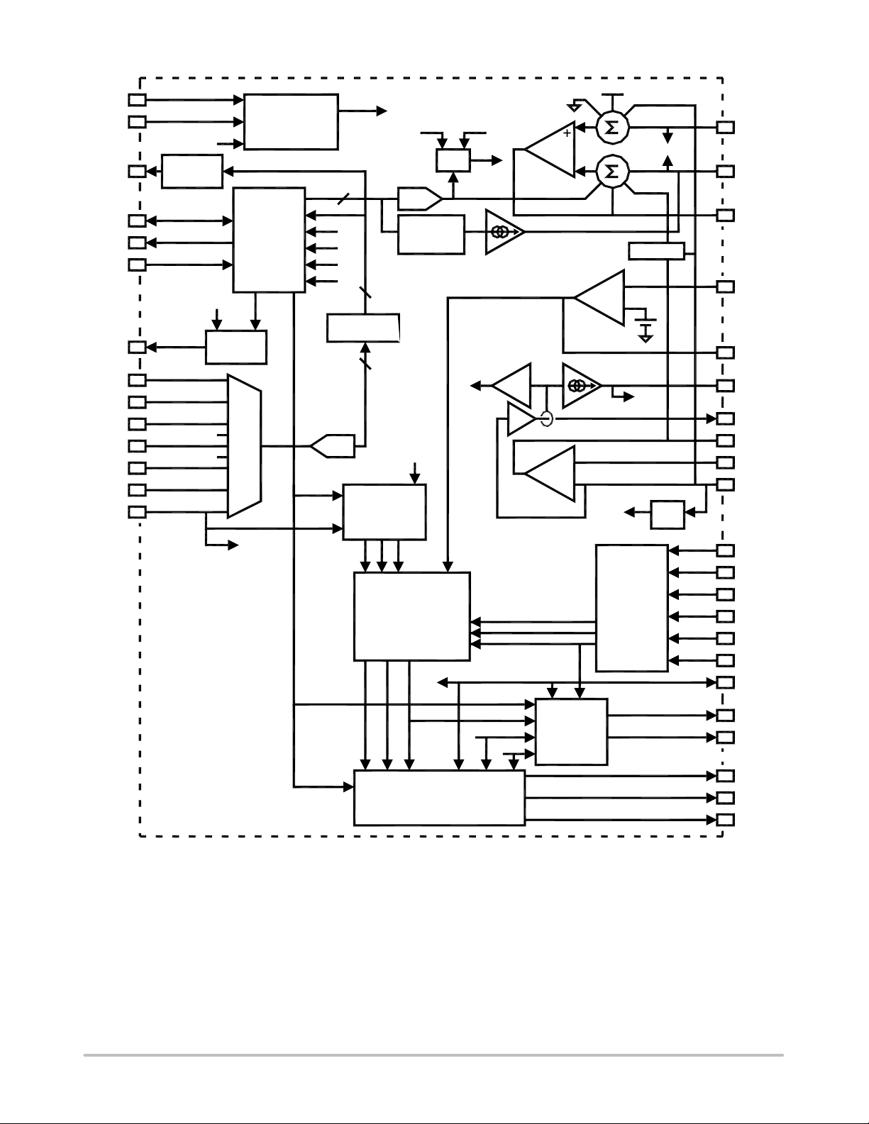
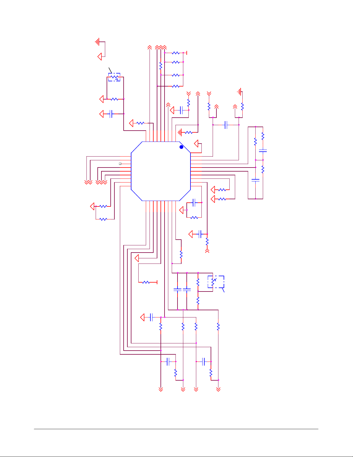
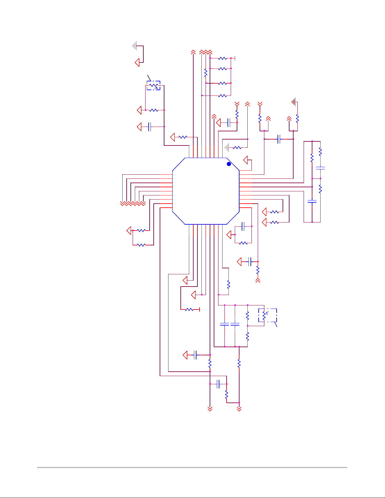
EN
VCC
VRHOT#
SDIO
ALERT#
SCLK
VR_RDY
ROSC
TSENSE
IMAX
INT_SEL
VBOOT
DGAIN
VRMP
1
2
VRMP
THERMAL
3
MONITOR
4
5
6
ENABLE
8
7
9
16
(VSP − VSN)
17
30
31
29
VR READY
IOUT
LOGIC
NCP81105
UVLO & EN
COMPARATORS
SVID
INTERFACE
& LOGIC
PS#
MUX
VRMP
ENABLE
DRVON
OCP
OVP
PS#
VRMP
PS#
NCP81105, NCP81105H
ENABLE
DATA
REGISTERS
ADC
OSCILLATOR
& RAMP
GENERATORS
VSP
DAC
DAC
FEED−
FORWARD
ENABLE
COMP
PWM
GENERATORS
PWM2
PWM3
PWM1
DRVON
POWER
STATE
GATE
VSN
OVP
OVP
DAC
OVERCURRENT
COMPARATORS
OCP
Buffer
DRVON
OVP
CURRENT
SENSE
AMP
PS#
OCP
DIFF
AMP
_
DAC
ERROR
AMP
OVERCURRENT
PROGRAMMING
_
+
ZERO
CURRENT
DETECTION
1.3V
CSREF
VSP
VSN
CSCOMP
SCALING
_
+
1.3V
CURRENT
MONITOR
IOUT
OVP
CURRENT
BALANCE
AMPLIFIERS
I2
I3
I1
MAX
OVP
36
35
34
33
32
28
27
26
25
24
23
22
21
20
19
18
15
11
14
13
12
10
VSP
VSN
DIFFOUT
FB
COMP
IOUT
ILIM
CSCOMP
CSSUM
CSREF
CSN2
CSP2
CSN3
CSP3
CSN1
CSP1
DRVON
SMOD
PWM1
PWM3
PWM2
OD#
Figure 1. Block Diagram
http://onsemi.com
2
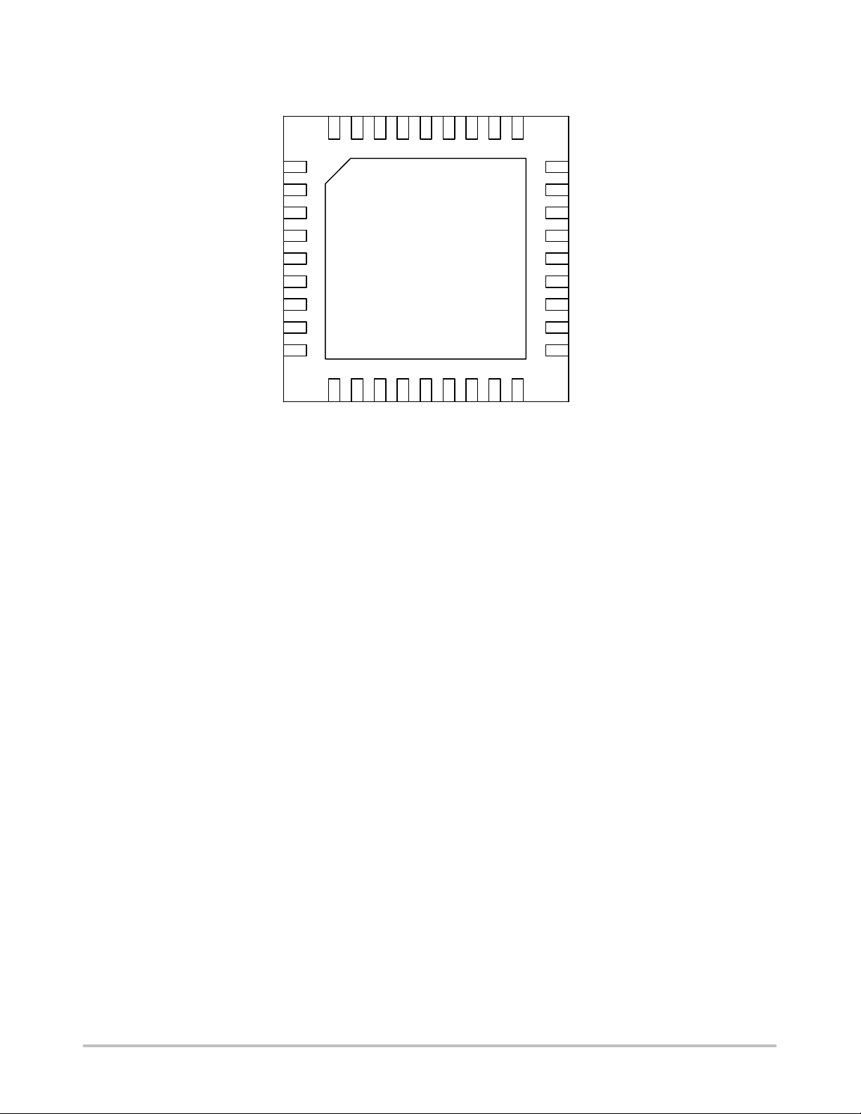
EN
VCC
VRHOT#
SDIO
ALERT#
SCLK
ROSC
VR_RDY
TSENSE
NCP81105, NCP81105H
VSP
VSN
DIFFOUTFBCOMP
36
35
34
33
1
2
3
4
5
6
7
8
9
10
TAB: GROUND
111
12
NCP81105
13
DGAIN
VBOOT
VRMP
IOUT
32
31
30
29
28
27
ILIM
26
CSCOMP
25
CSSUM
24
CSREF
23
CSN2
22
CSP2
21
CSN3
20
CSP3
19
CSN1
14
15
16
17
18
OD#
SMOD
PWM2
PWM3
PWM1
DRVON
Figure 2. Pin Connections
(Top View)
IMAX
CSP1
INT_SEL
http://onsemi.com
3

NCP81105, NCP81105H
PIN LIST AND DESCRIPTION
Pin
No.
1 EN Logic input. Logic high enables the NCP81105 and logic low disables it.
2 VCC Power for the internal control circuits. A decoupling capacitor must be connected from this pin to ground.
3 VR_HOT# Open drain (logic level) output for over−temperature reporting. Low indicates high temp.
4 SDIO Bidirectional Serial VID data interface.
5 ALERT# Open drain Serial VID ALERT# output.
6 SCLK Serial VID clock input.
7 ROSC This pin outputs a constant current. A resistance from this pin to ground programs the switching fre-
8 VR_RDY Open drain output. High indicates that the NCP81105 is regulating the output.
9 TSENSE Temperature sense input.
10 OD# Phase Disabling Output, tied to the Enable, SMOD or ZCD_EN# pin of phases 2 and 3 DrMOS. Except
11 SMOD Phase 1 Zero Cross Detection (ZCD) disable output. In PS2 & PS3, SMOD pulls LOW when phase 1
12 PWM2 PWM output to Phase 2 DrMOS
13 PWM3 PWM output to Phase 3 DrMOS
14 PWM1 PWM output to Phase 1 DrMOS
15 DRVON Enable output for DrMOS
16 IMAX During startup, a resistor from this pin to ground programs ICC_MAX.
17 INT_SEL During startup, a resistor from this pin to ground programs the low frequency compensator pole of the
18 CSP1 Positive input to phase 1 current sense amplifier for balancing phase currents
19 CSN1 Negative input to phase 1 current sense amplifier
20 CSP3 Positive input to phase 3 current sense amplifier for balancing phase currents
21 CSN3 Negative input to phase 3 current sense amplifier
22 CSP2 Positive input to phase 2 current sense amplifier for balancing phase currents
23 CSN2 Negative input to phase 2 current balance sense amplifier
24 CSREF Non−inverting input for the total output current sense amplifier. Also, the absolute OVP input.
25 CSSUM Inverting input of total output current sense amplifier.
26 CSCOMP Output of total output current sense amplifier.
27 ILIM Input to program the over−current shutdown threshold.
28 IOUT Total current monitor output. A resistor from this pin to ground calibrates SVID output current reporting.
29 VRMP VDC applied to this pin provides feed−forward compensation for the pulsewidth modulator. The current
30 VBOOT During startup, a resistor from this pin to ground programs the BOOT voltage
31 DGAIN During startup, a resistor from this pin to ground programs the scaling of the output Droop with respect to
32 COMP Output of the error amplifier.
33 FB Error amplifier voltage feedback input.
34 DIFFOUT Output of the differential remote sense amplifier.
35 VSN Inverting input to the differential remote sense amplifier (VSS sense).
36 VSP Non−inverting input to the differential remote sense amplifier (VCC sense).
37 GND Power supply return (QFN Flag)
Symbol Description
quency.
in PS0 mode, this output pulls low to disable the DrMOS if connected to an enable input. If connected to
a DrMOS SMOD or ZCD_EN# input, both HS & LS FETs are held off since PWM2 & PWM3 are also low.
Actively pulls high in PS0 mode.
inductor current is negative to perform (or allow the DrMOS ZCD function to perform) diode emulation,
and pulls HIGH when phase 1 inductor current is positive. In PS0 & PS1, SMOD stays high to force the
phase 1 DrMOS into Continuous Conduction.
NCP81105 voltage control feedback loop.
into this pin controls the slope of PWM ramp. A low voltage on this pin will inhibit NCP81105 startup.
the total output current signal produced between CSCOMP and CSREF.
http://onsemi.com
4
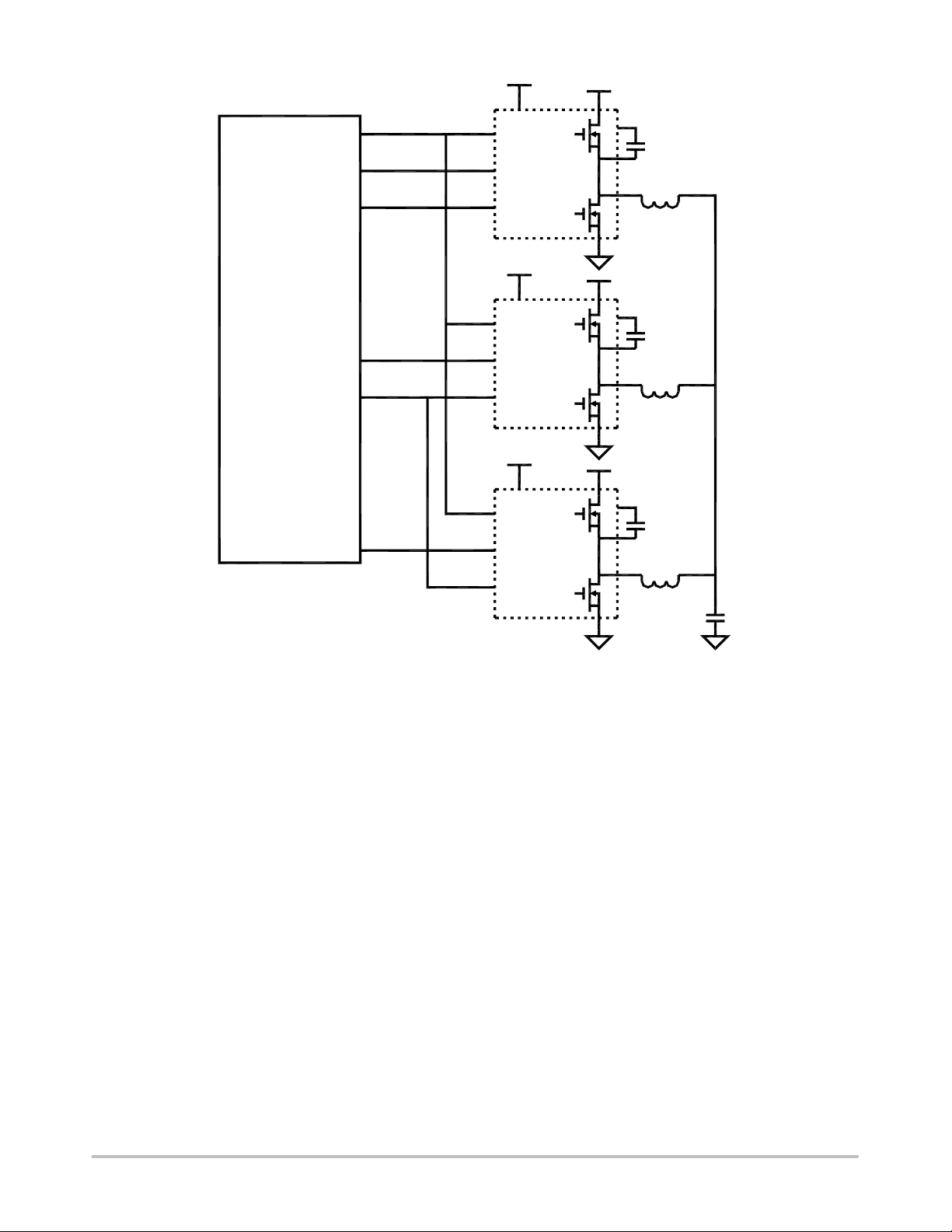
NCP81105, NCP81105H
DRVON
PWM1
SMOD
NCP81105
PWM2
PWM3
OD#
VCIN
EN
DRMOS
PWM
SMOD
VCIN
EN
DRMOS
PWM
SMOD
VCIN
EN
DRMOS
PWM
SMOD
VIN
BOOT
CB1
PHASE
VSWH
VIN
BOOT
CB2
PHASE
VSWH
VIN
BOOT
CB3
PHASE
VSWH
COUT
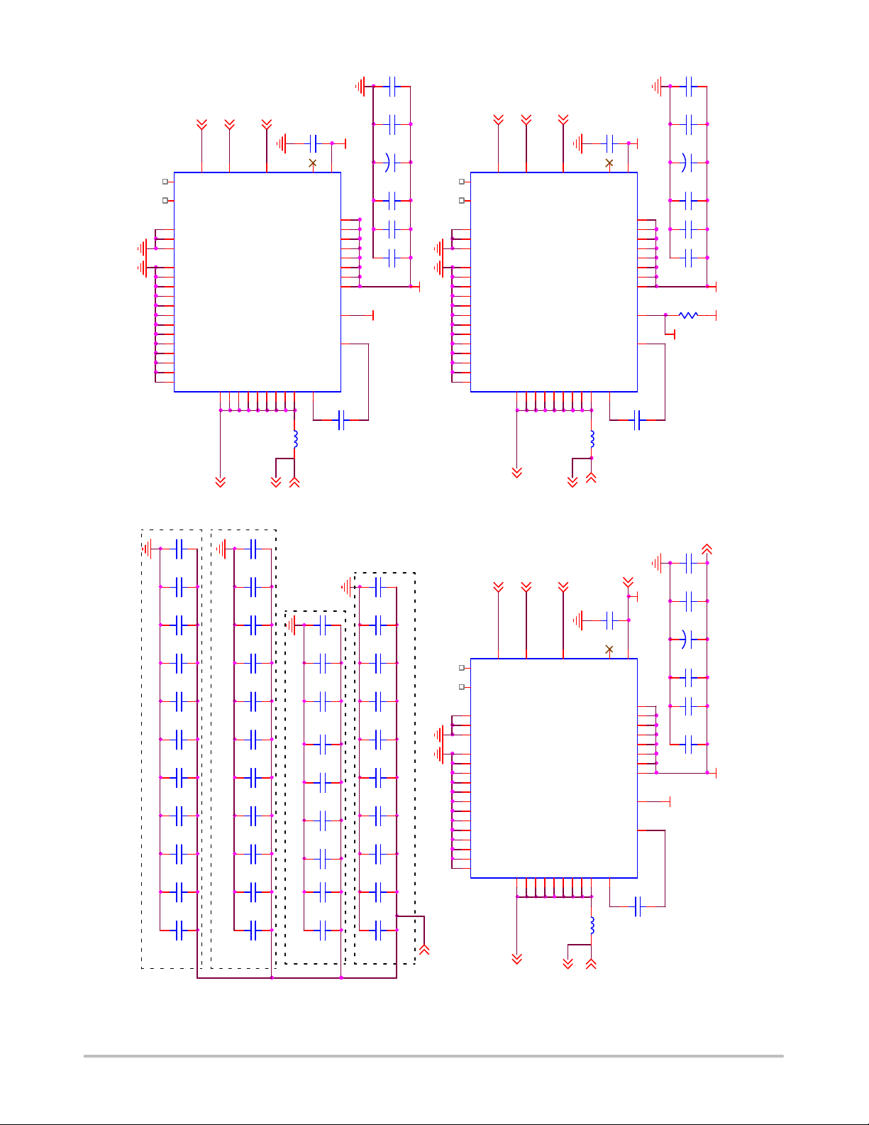
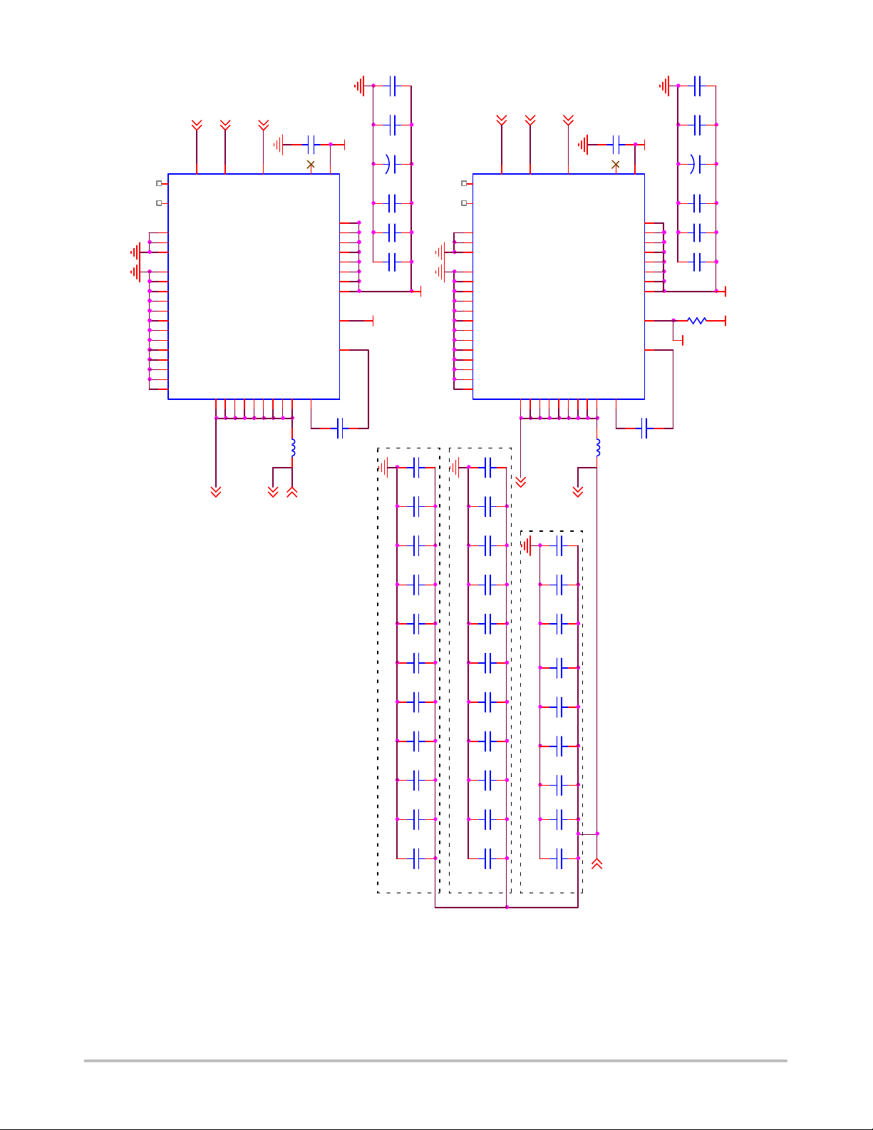
Figure 3. Three Phase Application Diagram
http://onsemi.com
5
close to L1
OD#
PWM2
PWM3
SMOD
place
1nF
DRVON
PWM1
R25
75.0K
RT12
220K
11.0K
R31
C81
INT_SEL
IMAX
NCP81105, NCP81105H
VR_RDY
ALERT
SCLK
SDIO
R162
130
R78
R155
130
43.2
TSENSE
10
OD#
11
SMOD
12
PWM2
13
PWM3
14
PWM1
15
DRVON
16
IMAX
17
INT_SEL
18
CSP1
VR_RDY
R154
80.6K
TSENSE9VRHOT#
VR_RDY8VCC2EN
ROSC
CSN3
CSN1
CSP3
20
19
SCLK
ALERT_VR
SDIO
ROSC
5
4
7
SCLK6ALERT#
SDIO
NCP81105
CSREF
CSN2
CSP2
22
24
21
23
R157
75.0
R156
VR_HOT
54.9
1uF
VCC
VR_HOT
3
1
DIFFOUT
U1
DGAIN
VBOOT
CSCOMP
CSSUM
ILIM
25
27
26
C79
EPAD
COMP
VRMP
IOUT
V_1P05_VCCP
ENABLE
V5S
4.99
ENABLE
R71
R161
1.0K
37
36
VSP
35
VSN
34
33
FB
32
31
30
29
28
0.15uF
C61
VCCU
IMON
VRMP
VCC_SENSE
R48 100
1nF
VSP
69.8K
VSS_SENSE
VSENSE
C51
VBOOT
R19
R34 100
VSN
DGAIN
DIFFOUT
R37 1.00K
FB
10pF
C57
COMPDIFFOUT
R50
37.4
C56
270pF
R43
4.75K
R26
51.1K
790kHz switching frequency
95A maximum output current
114A current limit
1.5mOhm loadline
1.7V boot voltage
CSP2
CSN1
CSN2
CSP3
CSP1
CSN3
10nF
C66
10.0
CSREF
R185
22nF
C80
CSCOMP
ILIM
17.4K
68pF
CSSUM
10.0K
R9
C156
100K
23.7K
R18
C155
680pF
R140
R38
0.01uF
73.2K
165K
10.0
1.0K
C82
RCS11
RCS12
R8
22nF
C83
R40
VDC
10.0K
RT11
220K
close
to L1
R139
100K
R10
place
R12
10.0
22nF
C85
100K
10.0K
R138
R27
CSN1
CSPP1
CSN3
CSPP3
CSN2
Figure 4. Three Phase Control Circuit Application
http://onsemi.com
6
CSPP2
PWM3
DRVON
OD#
NCP81105, NCP81105H
10uF
CA3
PWM1
DRVON
SMOD
10uF
CA1
6
36
41
5
37
16
17
18
19
20
21
22
23
24
25
26
27
28
LOCATE IN CENTER OF SOCKET rPGA989 CAVITY (PRIMARY SIDE)
GH
GL
CGND
CGND
CGND
PGND
PGND
PGND
PGND
PGND
PGND
PGND
PGND
PGND
PGND
PGND
PGND
PGND
22uF
22uF
22uF
22uF
22uF
22uF
22uF
22uF
22uF
22uF
22uF
C212
C213
C226
C227
C176
C177
C183
C184
C273
C271
C272
40
PWM
39
DISB#
VSWH31VSWH32VSWH33VSWH34VSWH
VSWH29VSWH
30
CSPP3
10uF
LOCATE IN CENTER OF SOCKET rPGA989 CAVITY (BOTTOM SIDE)
10uF
10uF
10uF
10uF
10uF
10uF
10uF
10uF
10uF
10uF
C29
1uF
ZCD_EN#1VCIN
NCP5338
U4
THWN
BOOT
PHASE
VSWH
VSWH
15
35
43
MPCG0740LR12
0.7mOhm
SW3
120nH
L3
CSNN3
VCCU
C214
C41
C48
LOCATE BETWEEN L1 & L2 (PRIMARY SIDE)
C49
C215
C216
C217
C204
C205
C206
C207
VIN
VIN
VIN
VIN
VIN
VIN
VIN
VIN
7
C52
22uF
C67
22uF
C68
22uF
C78
22uF
C84
22uF
C98
22uF
C99
22uF
C100
22uF
C196
DNP
2NC3
0.22uF
CB3
10uF
V5S
12
+
C3
33uF
C31
1uF
42
14
13
12
11
10
9
8
38
4
C28
C32
1uF
C9
1uF
VDC
THWN
Capacitor:
26 X 22uF(0805)
+ 11 X 10uF(0805)
C42
22uF
C43
DNP
C45
DNP
LOCATE BETWEEN L2 & L3 (PRIMARY SIDE)
C46
22uF
C95
22uF
C97
DNP
C189
22uF
C190
22uF
C210
22uF
C222
22uF
VCCU
39
40
DISB#
PWM
6
GH
36
GL
41
CGND
5
CGND
37
CGND
16
PGND
17
PGND
18
PGND
19
PGND
20
PGND
21
PGND
22
PGND
23
PGND
24
PGND
25
PGND
26
27
28
PGND
PGND
PGND
VSWH29VSWH
ZCD_EN#1VCIN
VSWH31VSWH32VSWH33VSWH34VSWH
30
Total VCORE Output
CSPP1
DRVON
PWM2
40
PWM
6
GH
36
GL
41
CGND
5
CGND
37
CGND
16
PGND
17
PGND
18
PGND
19
PGND
20
PGND
21
PGND
22
PGND
23
PGND
24
PGND
25
PGND
26
27
28
PGND
PGND
PGND
VSWH29VSWH
OD#
39
DISB#
ZCD_EN#1VCIN
VSWH31VSWH32VSWH33VSWH34VSWH
30
SW2SW1
CSPP2
NCP5338
U2
VSWH
35
43
0.7mOhm
120nH
CSN1
NCP5338
U3
VSWH
35
43
0.7mOhm
120nH
CSNN2
1uF
C5
2NC3
VIN
VIN
VIN
VIN
VIN
VIN
VIN
VIN
THWN
BOOT
PHASE
VSWH
7
15
MPCG0740LR12
0.22uF
L1
VCCU
V5S
C44
1uF
2NC3
VIN
VIN
VIN
VIN
VIN
VIN
VIN
VIN
THWN
BOOT
PHASE
VSWH
7
15
MPCG0740LR12
0.22uF
L2
VCCU
C4
42
14
13
12
11
10
9
8
38
4
V5SV5S
42
14
13
12
11
10
9
8
38
4
C37
10uF
33uF
1uF
1uF
1uF
1k
THWN
10uF
10uF
33uF
1uF
1uF
1uF
THWN
CB1
+
C1
C25
C26
C20
R121
CA2
CB2
+
C2
C27
C30
C36
12
V5S
VDC
12
VDCVDC
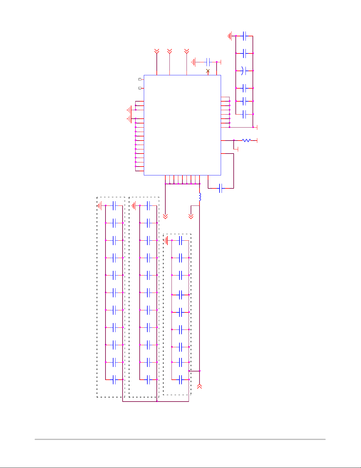
Figure 5. Three Phase Power Stage Circuit
http://onsemi.com
7
OD#
SMOD
PWM3
place
close to L1
RT12
220K
11.0K
R31
1nF
C81
TSENSE
10
11
12
13
14
15
16
17
INT_SEL
IMAX
18
DRVON
PWM1
R25
43.2K
NCP81105, NCP81105H
VR_RDY
ALERT
SCLK
VR_RDY
R154
80.6K
TSENSE9VRHOT#
VR_RDY8VCC2EN
ROSC
OD#
SMOD
PWM2
PWM3
PWM1
DRVON
IMAX
INT_SEL
CSP1
CSN1
CSP3
19
CSN3
20
SDIO
R78
43.2
VR_HOT
SCLK
ALERT_VR
SDIO
ROSC
5
4
7
SCLK6ALERT#
SDIO
NCP81105
CSSUM
CSREF
CSN2
CSP2
21
23
22
24
R162
R155
54.9
VR_HOT
3
U1
CSCOMP
25
130
130
R157
75.0
R156
C79
1uF
VCC
1
EPAD
VSN
DIFFOUT
COMP
DGAIN
VBOOT
VRMP
IOUT
ILIM
27
26
V_1P05_VCCP
V5S
4.99
R71
R161
1.0K
37
36
VSP
35
34
33
FB
32
31
30
29
28
0.15uF
ENABLE
ENABLE
C61
IMON
VCCU
VCC_SENSE
R48 100
VSP
69.8K
24.9K
VRMP
VSS_SENSE
VSENSE
C51
1nF
VBOOT
R19
R16
R34 100
VSN
DGAIN
DIFFOUT
R37 1.00K
FB
10pF
C57
COMPDIFFOUT
R50
37.4
C56
270pF
R43
4.75K
R26
51.1K
790kHz switching frequency
55A maximum output current
66A current limit
1.5mOhm loadline
1.7V boot voltage
CSN2
R128
1K
CSN1
CSP3
CSP1
CSN3
10nF
C66
V5S
10.0
CSREF
R185
22nF
C80
CSCOMP
ILIM
20.0k
68pF
CSSUM
10.0K
R9
R18
C156
680pF
49.9k
23.7K
C155
R140
R38
0.01uF
73.2K
165K
10.0
1.0K
C82
RCS11
RCS12
R8
22nF
C83
R40
VDC
10.0K
RT11
220K
close
to L1
R139
49.9k
R10
place
CSN1
CSPP1
CSN3
CSPP3
Figure 6. Two Phase Control Circuit Application
http://onsemi.com
8
PWM3
DRVON
OD#
NCP81105, NCP81105H
10uF
CA3
PWM1
DRVON
SMOD
10uF
CA1
C29
1uF
39
40
DISB#
PWM
6
GH
36
GL
41
CGND
5
CGND
37
CGND
16
PGND
17
PGND
18
PGND
19
PGND
20
PGND
21
PGND
22
PGND
23
PGND
24
PGND
25
PGND
26
27
28
PGND
PGND
PGND
VSWH29VSWH
CSPP3
ZCD_EN#1VCIN
NCP5338
U4
VSWH31VSWH32VSWH33VSWH34VSWH
30
SW3
VSWH
35
0.7mOhm
120nH
CSNN3
VSWH
15
43
MPCG0740LR12
VCCU
VIN
VIN
VIN
VIN
VIN
VIN
VIN
VIN
THWN
BOOT
PHASE
7
0.22uF
L3
V5S
2NC3
42
14
13
12
11
10
9
8
38
4
C28
10uF
33uF
1uF
1uF
1uF
THWN
LOCATE IN CENTER OF SOCKET rPGA989 CAVITY (PRIMARY SIDE)
CB3
+
C3
C31
C32
C9
12
C212
22uF
C213
22uF
VDC
PWM
6
GH
36
GL
41
CGND
5
CGND
37
CGND
16
PGND
17
PGND
18
PGND
19
PGND
20
PGND
21
PGND
22
PGND
23
PGND
24
PGND
25
PGND
26
PGND
27
PGND
28
PGND
C214
10uF
LOCATE IN CENTER OF SOCKET rPGA989 CAVITY (BOTTOM SIDE)
C41
10uF
40
DISB#
VSWH29VSWH
CSPP1
39
VSWH31VSWH32VSWH33VSWH34VSWH
30
1uF
C5
ZCD_EN#1VCIN
VIN
VIN
VIN
VIN
U2
THWN
BOOT
PHASE
VSWH
VSWH
15
35
43
7
MPCG0740LR12
120nH
L1
VIN
VIN
VIN
VIN
NCP5338
SW1
CSN1
0.7mOhm
V5S
2NC3
42
14
13
12
11
10
9
8
38
4
0.22uF
C4
CB1
10uF
+
C1
33uF
1uF
1uF
1uF
R121
1k
THWN
12
C25
C26
C20
VDC
V5S
C226
22uF
C227
22uF
C176
22uF
C177
22uF
C183
22uF
C184
22uF
C273
22uF
C271
22uF
C272
22uF
C48
10uF
C49
10uF
C215
10uF
C216
10uF
C217
10uF
C204
10uF
C205
10uF
C206
10uF
C207
10uF
LOCATE BETWEEN L1 & L2 (PRIMARY SIDE)
Figure 7. Two Phase Power Stage Circuit
C52
22uF
C67
22uF
C68
22uF
C78
22uF
C84
22uF
C98
22uF
C99
22uF
C100
22uF
C196
22Uf
Total VCORE Output
Capacitor:
20 X 22uF(0805)
+ 11 X 10uF(0805)
VCCU
http://onsemi.com
9
close to L1
PWM1
OD#
PWM2
PWM3
SMOD
25.5K
NCP81105, NCP81105H
VR_RDY
ALERT
SCLK
place
220K
11.0K
1nF
DRVON
IMAX
R25
RT12
R31
C81
INT_SEL
TSENSE
10
OD#
11
SMOD
12
PWM2
13
PWM3
14
PWM1
15
DRVON
16
IMAX
17
INT_SEL
18
CSP1
R154
80.6K
TSENSE9VRHOT#
CSN1
R78
43.2
VR_RDY
SCLK
ALERT_VR
ROSC
5
7
SCLK6ALERT#
VR_RDY8VCC2EN
ROSC
CSN3
CSN2
CSP3
CSP2
21
19
23
20
22
SDIO
R162
R155
R157
R156
VR_HOT
54.9
SDIO
VR_HOT
3
4
SDIO
NCP81105
U1
CSCOMP
CSSUM
CSREF
24
25
130
130
75.0
C79
1uF
VCC
1.0K
1
EPAD
VSP
VSN
DIFFOUT
COMP
DGAIN
VBOOT
VRMP
IOUT
ILIM
27
26
V_1P05_VCCP
ENABLE
V5S
4.99
ENABLE
R71
R161
37
36
35
34
33
FB
32
31
30
29
28
0.15uF
C61
IMON
VCCU
VCC_SENSE
R48 100
VSP
69.8K
24.9K
VRMP
VSS_SENSE
VSENSE
C51
1nF
VBOOT
R19
R16
R34 100
VSN
DGAIN
DIFFOUT
R37 1.00K
FB
10pF
C57
COMPDIFFOUT
R50
37.4
C56
270pF
R43
4.75K
R26
51.1K
CSP1
790kHz switching frequency
32A maximum output current
39A current limit
2.0mOhm loadline
1.7V boot voltage
CSN3
R128
1K
CSN1
10nF
C66
V5S
10.0
CSREF
CSSUM
R185
22nF
CSN1
CSCOMP
ILIM
8.87K
68pF
C156
C80
10.0K
R9
23.7K
R18
C155
680pF
75.0K
CSPP1
R38
0.01uF
73.2K
165K
R140
1.0K
C82
RCS11
RCS12
R40
VDC
RT11
220K
close
to L1
place
Figure 8. Single Phase Control Circuit Application
http://onsemi.com
10
NCP81105, NCP81105H
DRVON
PWM1
40
DISB#
PWM
6
GH
36
GL
41
CGND
5
CGND
37
CGND
16
PGND
17
PGND
18
PGND
19
PGND
20
PGND
21
PGND
22
PGND
23
PGND
24
PGND
25
PGND
26
27
28
PGND
PGND
PGND
VSWH29VSWH
SMOD
39
ZCD_EN#1VCIN
NCP5338
VSWH31VSWH32VSWH33VSWH34VSWH
30
SW1
VSWH
35
0.7mOhm
1uF
U2
VSWH
15
43
120nH
C5
VIN
VIN
VIN
VIN
VIN
VIN
VIN
VIN
THWN
BOOT
PHASE
7
V5S
2NC3
42
14
13
12
11
10
9
8
38
4
MPCG0740LR12
0.22uF
C4
L1
CA1
10uF
CB1
10uF
+
C1
33uF
1uF
1uF
1uF
1k
THWN
12
C25
C26
C20
VDC
V5S
R121
LOCATE IN CENTER OF SOCKET rPGA989 CAVITY (PRIMARY SIDE)
C212
22uF
C213
22uF
C226
22uF
C227
22uF
C176
22uF
C177
22uF
C183
22uF
C184
22uF
C273
22uF
C271
22uF
C214
10uF
LOCATE IN CENTER OF SOCKET rPGA989 CAVITY (BOTTOM SIDE)
C41
10uF
C48
10uF
C49
10uF
C215
10uF
C216
10uF
C217
10uF
C204
10uF
C205
10uF
C206
10uF
CSPP1
LOCATE NEAR L1 (PRIMARY SIDE)
C52
DNP
C67
DNP
C68
DNP
C78
22uF
C84
22uF
C98
22uF
C99
22uF
C100
22uF
CSN1
Total VCORE Output
Capacitor:
16 X 22uF(0805)
+ 11 X 10uF(0805)
C196
C272
22uF
10uF
C207
DNP
VCCU
Figure 9. Single Phase Power Stage Circuit
http://onsemi.com
11
 Loading...