

查询NCV33204供应商
NCP5661, NCV5661
Low Output Voltage,
Ultra−Fast 1.0 A Low Dropout
Linear Regulator with Enable
The NCP5661/NCV5661 is a high performance, low dropout linear
regulator designed for high power applications that require up to 1.0 A
current. It is offered in both fixed and adjustable output versions. With
output voltages as low as 0.9 V and ultra−fast response times for load
transients, the NCP5661/NCV5661 also provides additional features
such as Enable and Error Flag (for the fixed output version),
increasing the utility of these devices. A thermally robust, 5 pin
DPAK, combined with an architecture that offers low ground current
(independent of load), provides for a superior high−current LDO
solution.
Features
• Ultra−Fast Transient Response (Settling Time: 1−3 ms)
• Low Noise Without Bypass Capacitor (26 mV
• Low Ground Current Independent of Load (3.0 mA Maximum)
• Fixed/Adjustable Output Voltage Versions
• Enable Function
• Error Flag (Fixed Output Version)
• Current Limit Protection
• Thermal Protection
• 0.9 V Reference Voltage for Ultra−Low Output Operation
• Power Supply Rejection Ratio > 65 dB
• NCV Prefix for Automotive and Other Applications Requiring Site
and Control Changes
• These are Pb−Free Devices
rms)
http://onsemi.com
1
5
DPAK−5
CENTER LEAD CROP
CASE 175AA
Tab = Ground
Pin: 1. Enable
2. V
in
3. Ground
4. V
out
5. Adj (Adjustable Output)
5. Error Flag (Fixed Output)
x = A for Adjustable Version
B for Fixed 1.2 V
C for Fixed 3.3 V
A = Assembly Location
L = Wafer Lot
Y = Year
WW = Work Week
G = Pb−Free
MARKING
MARKING
DIAGRAM
DIAGRAM
661xG
ALYWW
Applications
• Servers
• ASIC Power Supplies
• Post Regulation for Power Supplies
• Constant Current Source
• Networking Equipment
• Gaming and STB Modules
© Semiconductor Components Industries, LLC, 2005
August, 2005 − Rev. 4
See detailed ordering and shipping information in the package
ORDERING INFORMATION
dimensions section on page 10 of this data sheet.
1 Publication Order Number:
NCP5661/D
NCP5661, NCV5661
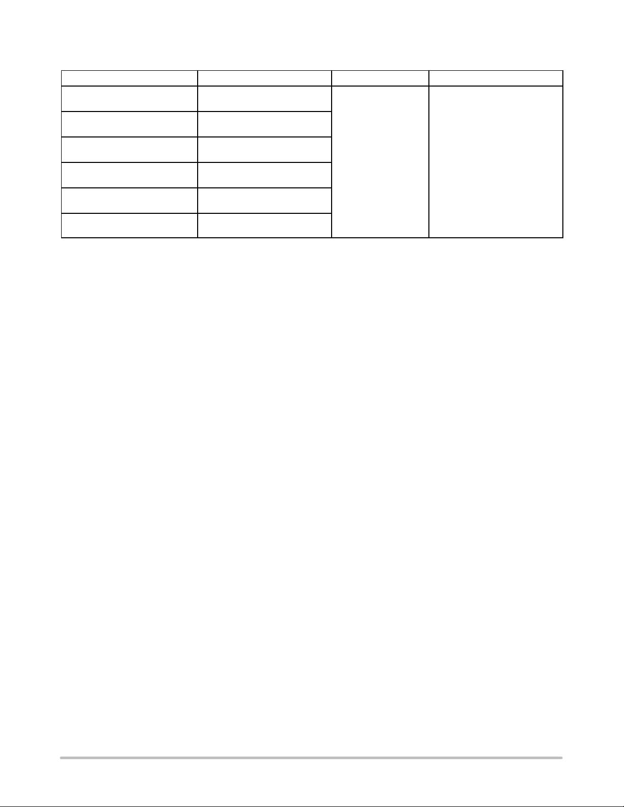
PIN FUNCTION DESCRIPTION
Pin
Adj/Fixed
1 Enable This pin allows for on/off control of the regulator. To disable the device, connect to Ground. If this
2 V
3 Ground Power Supply Ground
4 V
5 Adj
5 Error Flag
MAXIMUM RATINGS
Input Voltage V
Output Pin Voltage V
Adjust Pin Voltage V
Enable Pin Voltage V
Error Flag Voltage V
Error Flag Current I
Thermal Characteristics
Thermal Resistance, Junction−to−Air
Thermal Resistance, Junction−to−Case
Operating Junction Temperature Range T
Storage Temperature Range T
Maximum ratings are those values beyond which device damage can occur. Maximum ratings applied to the device are individual stress limit
values (not normal operating conditions) and are not valid simultaneously. If these limits are exceeded, device functional operation is not implied,
damage may occur and reliability may be affected.
NOTE: This device series contains ESD protection and exceeds the following tests:
The maximum package power dissipation is:
The bipolar process employed for this IC is fully characterized and rated for reliable 18 V V
For open−circuit to short−circuit transient,
P
DTransient
Pin Name Description
function is not in use, connect to Vin.
in
out
Positive Power Supply Input Voltage
Regulated Output Voltage
This pin is connected to the resistor divider network and programs the output voltage.
(Adjustable Version)
An Error Flag is triggered when the output voltage is out of regulation excluding transient signals
(Fixed Version)
that may occur. Requires a pullup resistor f 100 kW.
Rating Symbol Value Unit
in
out
adj
en
ef
ef
R
θ
JA
R
θ
JC
J
stg
18 V
−0.3 to Vin +0.3 V
−0.3 to Vin +0.3 V
−0.3 to Vin +0.3 V
−0.3 to Vin +0.3 V
3.0 mA
100
8.0
−40 to +150 °C
−55 to +150 °C
Human Body Model (HBM) JESD 22−A114−B
Machine Model (MM) JESD 22−A115−A.
T
P
+
D
J(max)
R
qJA
* T
A
operation. To avoid damaging
CCmax
the part or degrading it’s reliability, power dissipation transients should be limited to under 20 W for DPAK.
= V
CCmax
* ISC.
°C/W
http://onsemi.com
2
NCP5661, NCV5661
ELECTRICAL CHARACTERISTICS
(V
− V
= 1.5 V, for typical values TJ = 25°C, for min/max values TJ = −40°C to 125°C, Cin = C
in
out
Characteristic
ADJUSTABLE OUTPUT VERSION
Input Voltage V
Output Noise Voltage V
Output Voltage Accuracy
T
= 25°C (I
J
TJ = −20 to +125°C (I
TJ = −40 to +150°C (I
= 10 mA to 1.0 A)
out
= 10 mA to 1.0 A)
out
= 10 mA to 1.0 A)
out
Adjustable Pin Input Current I
Line Regulation (I
Load Regulation (10 mA < I
Dropout Voltage (I
= 10 mA, V
out
= 1.0 A) V
out
+1.5 V < Vin < 7.0 V) REG
out
< 1.0 A) REG
out
Peak Output Current Limit I
Internal Current Limitation I
Ripple Rejection (120 Hz)
Ripple Rejection (1.0 kHz)
Thermal Shutdown (Guaranteed by Design) T
Ground Current
I
= 1.0 A
out
Disabled State
Enable Input Threshold Voltage
Voltage Increasing, On State, Logic High
Voltage Decreasing, Off State, Logic Low
Enable Input Current
Enable Pin Voltage = 0.3 V
Enable Pin Voltage = 1.3 V
Symbol Min Typ Max Unit
max
min
in
n
V
out
−1.5%
adj
line
load
DO
out
lim
RR −
SHD
I
q
I
qds
V
en
I
en
= 150 mF unless otherwise noted.)
out
2.0 − 9.0 V
− 26 −
−1%
−
0.9
−2%
−
+1%
+1.5%
+2%
mV
− 40 − nA
− 0.03 − %
− 0.03 − %
− 1.0 1.3 V
1.0 − − A
− 1.5 − A
70
−
65
−
−
− 160 − °C
−
−
1.3
−
−
−
1.3
10
−
−
0.5
0.5
3.0
300
−
0.3
−
−
rms
V
dB
mA
mA
V
mA
http://onsemi.com
3

NCP5661, NCV5661
ELECTRICAL CHARACTERISTICS
(V
− V
= 1.5 V, for typical values TJ = 25°C, for min/max values TJ = −40°C to 125°C, Cin = C
in
out
Characteristic
FIXED OUTPUT VOLTAGE
Input Voltage V
Output Noise Voltage (V
= 0.9 V) V
out
Output Voltage Accuracy (Note 1)
T
= 25°C (I
J
TJ = −20 to +125°C (I
TJ = −40 to +150°C (I
Line Regulation (I
Load Regulation (10 mA < I
Dropout Voltage (I
= 10 mA to 1.0 A)
out
out
out
= 10 mA to 1.0 A)
out
= 10 mA to 1.0 A)
out
= 10 mA, V
+1.5 V < Vin < 7.0 V) REG
out
< 1.0 A) REG
out
= 1.0 A) V
Peak Output Current Limit I
Internal Current Limitation I
Ripple Rejection (120 Hz)
Ripple Rejection (1.0 kHz)
Thermal Shutdown (Guaranteed by Design) T
Ground Current
I
= 1.0 A
out
Disabled State
Enable Input Threshold Voltage
Voltage Increasing, On State, Logic High
Voltage Decreasing, Off State, Logic Low
Enable Input Current
Enable Pin Voltage = 0.3 V
Enable Pin Voltage = 1.3 V
Error Flag (Fixed Output)
1.2 V Output
3.3 V Output
Error Flag Output Low Voltage Saturation (Ief = 1.0 mA) V
Error Flag Leakage I
Error Flag Blanking Time (Note 2) T
1. Fixed output voltages available at 0.9 V, 1.2 V, 1.5 V, 1.8 V, 2.5 V, 3.0 V, 3.3 V per request.
2. Can be disabled per customer request.
Symbol Min Typ Max Unit
in
n
V
out
−1.5%
line
load
DO
out
lim
RR −
SHD
I
q
I
qds
V
en
I
en
max
min
V
eflt
efdo
efleak
ef
= 150 mF unless otherwise noted.)
out
2.0 − 9.0 V
− 26 −
−1%
−2%
−
V
out
−
+1%
+1.5%
+2%
mV
− 0.03 − %
− 0.2 − %
− 1.0 1.3 V
1.0 − − A
− 1.5 − A
70
−
65
−
−
− 160 − °C
−
−
1.3
−
−
−
1.3
30
−
−
0.5
0.5
3.0
300
−
0.3
−
−
% of V
88
90
92
94
97
97
− 200 − mV
− 1.0 −
− 50 −
rms
V
dB
mA
mA
V
mA
out
mA
ms
http://onsemi.com
4

NCP5661, NCV5661
V
in
IN
ON
Voltage
V
out
ǒ
V
ref
Reference
Block
Ǔ
* 1
C
in
R1 + R2
*CC = 5.0 to 200 pF
R3
R4
V
ref
= 0.9 V
Output
Stage
GND
GND
Enable
Block
EN
OFF
V
out
ADJ
R1
R2
CC*
C
out
Figure 1. Typical Schematic, Adjustable Output Version
V
in
IN
ON
Cc
V
EF
EN
OFF
out
Rflag = 100 kW
C
out
Voltage
Reference
C
in
Block
R3
R4
V
ref
= 0.9 V
Output
Stage
Error
Flag
GND
Enable
Block
R1
R2
GND
Figure 2. Typical Schematic, Fixed Output Version
http://onsemi.com
5

NCP5661, NCV5661
1.00
1.2
0
0
t
1.0
0.8
0.6
0.4
, DROPOUT VOLTAGE (V)
DO
0.2
V
0
−40 −20 0 20 40 60 80 100 120 140
TJ, JUNCTION TEMPERATURE (°C)
Figure 3. Dropout Voltage vs. Temperature Figure 4. Dropout Voltage vs. Output Current
3.5
3.0
2.5
2.0
1.5
, DROPOUT VOLTAGE (V)
DO
V
0.95
0.90
0.85
0.80
0.75
0.70
0.0 0.1
2.0
1.8
1.6
1.4
V
= 2.5 V Adjustable
out
Cin = 150 mF
C
= 10 to 150 mF
out
TJ = 25°C
0.2 0.3 0.4 0.5 0.6 0.7 0.8 0.9 1.0
I
, OUTPUT CURRENT (A)
out
1.0
, GROUND CURRENT (mA)
0.5
GND
I
0
−40 −20 0 20 40 60 80 100 120 140
TJ, JUNCTION TEMPERATURE (°C)
Figure 5. Ground Current vs. Temperature Figure 6. Short Circuit Current Limit vs.
0.95
0.90
0.85
0.80
, OUTPUT VOLTAGE (V)
out
0.75
V
0.70
1.0 2.0 3.0 4.0 5.0 6.0 7.0 8.0 9.0
Vin, INPUT VOLTAGE (V)
I
= 10 mA
out
Cin = 150 mF
C
= 1.0 to 150 mF
out
TJ = 25°C
1.2
, SHORT CIRCUIT LIMIT (A)
SC
I
1.0
−40 −20 0 20 40 60 80 100 120 14
TJ, JUNCTION TEMPERATURE (°C)
Temperature
0.900
0.898
0.896
0.894
Vin = 3.3 V
I
, OUTPUT VOLTAGE (V)
0.892
out
V
Cin = 150 mF
C
TJ = 25°C
0.890
0.0 0.2 0.4 0.6 0.8 1.
I
, OUTPUT CURRENT (A)
out
= 1.0 A maximum
out
= 1.0 to 150 mF
out
Figure 7. Output Voltage vs. Input Voltage Figure 8. Output Voltage vs. Output Load Curren
http://onsemi.com
6

NCP5661, NCV5661
0.9
00
90
0
0.8
TA = 25°C
L = 25 mm Copper
0.7
0.6
0.5
0.4
0.3
0.2
OUTPUT CURRENT (A)
0.1
0.0
INPUT−OUTPUT VOLTAGE DIFFERENTIAL (V)
Figure 9. Output Current vs. Input−Output
Voltage Differential
100
90
80
/ǨHz)
70
rms
60
50
40
30
20
NOISE DENSITY (nV
10
0
Start: 100 Hz Stop: 100 kHz
F, FREQUENCY (kHz)
Vin = 3.3 V
V
out
I
out
Cin = 150 mF
C
out
TJ = 25°C
1412468
= 0.9 V
= 10 mA
= 150 mF
80
70
60
50
40
30
20
RR, RIPPLE REJECTION (dB)
10
Vin = 4.0 V
V
out
Cin = 0 mF
C
out
TJ = 25°C
0
20161020
Figure 10. Ripple Rejection vs. Frequency
100
90
80
/ǨHz)
70
rms
60
50
40
30
20
NOISE DENSITY (nV
10
0
Start: 100 Hz Stop: 100 kHz
= 0.9 V
= 1.0 mF
I
= 1.0 A
out
F, FREQUENCY (kHz)
Vin = 3.3 V
V
I
Cin = 150 mF
C
TJ = 25°C
F, FREQUENCY (kHz)
I
out
1001010
= 0.9 V
out
= 1.0 A
out
= 150 mF
out
= 10 mA
10
Figure 11. Noise Density vs. Frequency
1000
100
10 mF
Unstable
10
ESR (W)
1.0
100 mF
150 mF
0.10
Stable
0.01
100 1000
0 200 300 400 500 600 700 800 900
OUTPUT CURRENT (mA)
Figure 13. 1.2 Volt Output Stability with Output
Capacitor ESR
1000
100
10
ESR (W)
1.0
0.10
0.01
0 200 300 400 500 600 700 800 900
http://onsemi.com
7
Figure 12. Noise Density vs. Frequency
150 mF
100 mF
10 mF
100 100
OUTPUT CURRENT (mA)
Unstable
Stable
Figure 14. 3.3 Volt Output Stability with Output
Capacitor ESR
out
V
10 mV/Div
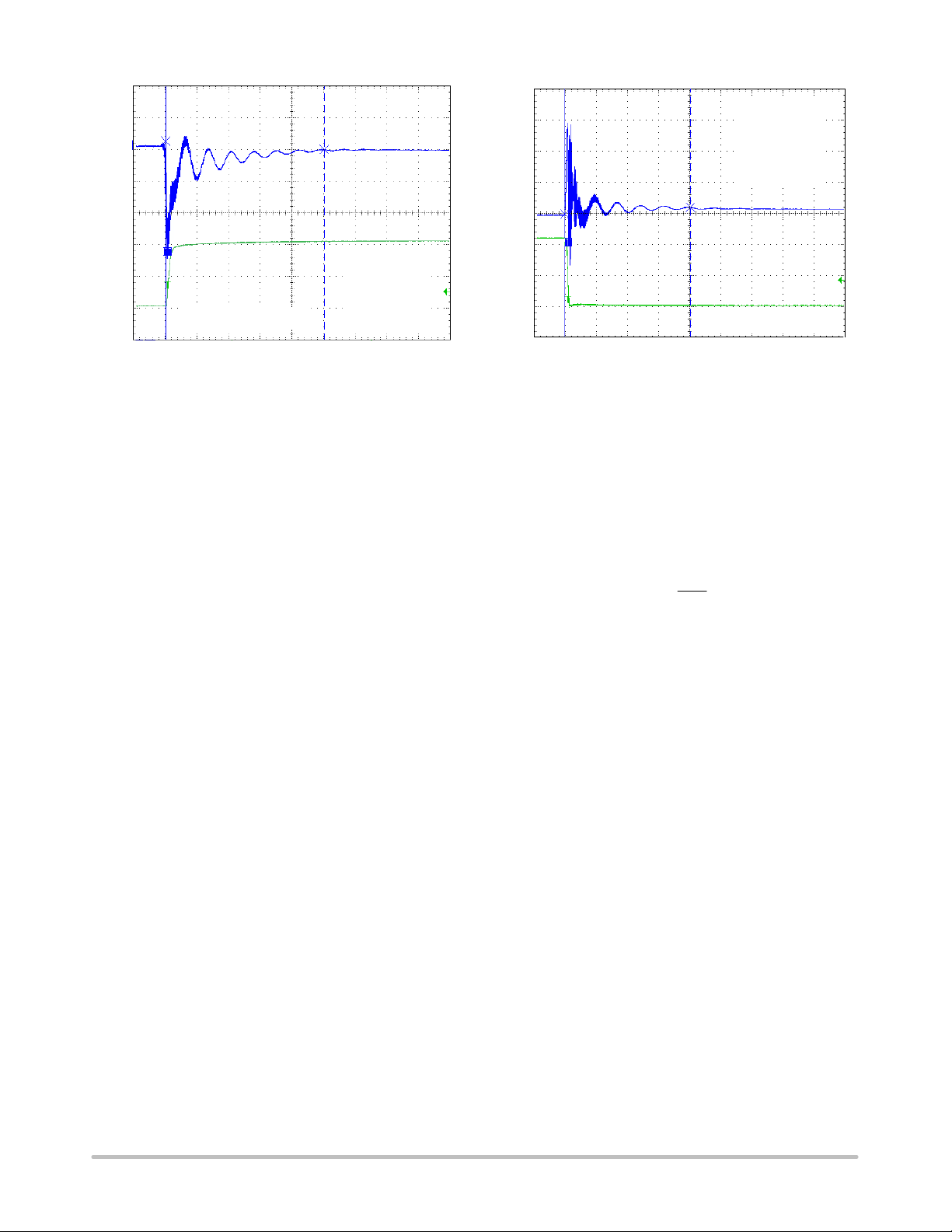
NCP5661, NCV5661
out
V
10 mV/Div
Vin = 4.0 V
V
= 0.9 V
out
Cin = 150 mF
C
= 150 mF
out
TJ = 25°C
out
I
0.5 A/Div
I
= 10 mA to 1.0 A
out
TIME (1.0 ms/Div)
Figure 15. Load Transient Response
Vin = 4.0 V
V
= 0.9 V
out
Cin = 150 mF
C
= 150 mF
out
TJ = 25°C
APPLICATION INFORMATION
The NCP5661 is a high performance low dropout 1.0 A
linear regulator suitable for high power applications,
featuring an ultra−fast response time and low noise without
a bypass capacitor. It is offered in both fixed and adjustable
output versions with voltages as low as 0.9 V. Additional
features, such as Enable and Error Flag (fixed output
version) increase the utility of the NCP5661. It is thermally
robust and includes the safety features necessary during a
fault condition, which provide for an attractive high current
LDO solution for server, ASIC power supplies, networking
equipment applications, and many others.
Input Capacitor
The recommended input capacitor value is a 150 mF
OSCON with an Equivalent Series Resistance (ESR) of
50 mW. It is especially required if the power source is
located more than a few inches from the NCP5661. This
capacitor will reduce device sensitivity and enhance the
output transient response time. The PCB layout is very
important and in order to obtain the optimal solution, the V in
and GND traces should be sufficiently wide to minimize
noise and unstable operation.
Output Capacitor
Proper output capacitor selection is required to maintain
stability. The NCP5661 is guaranteed to be stable at an
output capacitance of, C
> 10 mF with an ESR < 300 mW
out
over the output current range of 10 mA to 1.0 A. For PCB
layout considerations, place the recommended ceramic
capacitor close to the output pin and keep the leads short.
This should help ensure ultra−fast transient response times.
out
I
0.5 A/Div
I
= 1.0 A to 10 mA
out
TIME (1.0 ms/Div)
Figure 16. Load Transient Response
Adjustable Output Operation
The application circuit for the adjustable output version is
shown in Figure 1. The reference voltage is 0.9 V and the
adjustable pin current is typically 40 nA. A resistor divider
network, R1 and R2, is calculated using the following
formula:
R1 + R2
Current Limit Operation
ǒ
V
ref
* 1
Ǔ
V
out
As the peak output current increases beyond its limitation,
the device is internally clampled to 1.5 A, thus causing the
output voltage to decrease and go out of regulation. This
allows the device never to exceed the maximum power
dissipation.
Error Flag Operation
The Error Flag pin on the NCP5661 will produce a logic
Low when it drops below the nominal output voltage. Refer
to the electrical characteristics for the threshold values at
which point the Error Flag goes Low. When the NCP5661
is above the nominal output voltage, the Error Flag will
remain at logic High.
The external pullup resistor needs to be connected
between Vin (Pin 1) and the Error Flag pin (Pin 5). A resistor
of approximately 100 kW is recommended to minimize the
current consumption. No pullup resistor is required if the
Error Flag output is not being used.
http://onsemi.com
8

NCP5661, NCV5661
NCP5661 Evaluation Board
Figure 17. Test Board used for Evaluation
http://onsemi.com
9
NCP5661, NCV5661
ORDERING INFORMATION
Device Nominal Output Voltage Package Shipping†
NCP5661DTADJRKG Adj
NCP5661DT12RKG (Note 3) Fixed, 1.2 V
NCP5661DT33RKG (Note 3) Fixed, 3.3 V
NCV5661DTADJRKG Adj
NCV5661DT12RKG (Note 3) Fixed, 1.2 V
NCV5661DT33RKG (Note 3) Fixed, 3.3 V
3. Fixed output voltages available at 0.9 V, 1.5 V, 1.8 V, 2.5 V, 3.0 V per request.
†For information on tape and reel specifications, including part orientation and tape sizes, please refer to our Tape and Reel Packaging
Specifications Brochure, BRD8011/D.
(Pb−Free)
(Pb−Free)
(Pb−Free)
DPAK 2500 Tape & Reel
(Pb−Free)
(Pb−Free)
(Pb−Free)
http://onsemi.com
10

NCP5661, NCV5661
PACKAGE DIMENSIONS
DPAK−5
CENTER LEAD CROP
CASE 175AA−01
ISSUE A
SEATING
−T−
PLANE
B
V
S
R
A
1234 5
K
F
L
D
5 PL
G
0.13 (0.005) T
C
E
R1
Z
U
J
H
M
NOTES:
1. DIMENSIONING AND TOLERANCING
PER ANSI Y14.5M, 1982.
2. CONTROLLING DIMENSION: INCH.
DIM MIN MAX MIN MAX
A 0.235 0.245 5.97 6.22
B 0.250 0.265 6.35 6.73
C 0.086 0.094 2.19 2.38
D 0.020 0.028 0.51 0.71
E 0.018 0.023 0.46 0.58
F 0.024 0.032 0.61 0.81
G 0.180 BSC 4.56 BSC
H 0.034 0.040 0.87 1.01
J 0.018 0.023 0.46 0.58
K 0.102 0.114 2.60 2.89
L 0.045 BSC 1.14 BSC
R 0.170 0.190 4.32 4.83
R1 0.185 0.210 4.70 5.33
S 0.025 0.040 0.63 1.01
U 0.020 −−− 0.51 −−−
V 0.035 0.050 0.89 1.27
Z 0.155 0.170 3.93 4.32
MILLIMETERSINCHES
SOLDERING FOOTPRINT*
6.4
0.252
5.8
0.228
10.6
0.417
SCALE 4:1
*For additional information on our Pb−Free strategy
and soldering details, please download the
ON Semiconductor Soldering and Mounting
Techniques Reference Manual, SOLDERRM/D.
2.2
0.086
0.34
0.013
0.8
0.031
ǒ
inches
5.36
0.217
mm
Ǔ
http://onsemi.com
11
NCP5661, NCV5661
The products described herein (NCP5661/NCV5661), may be covered by one or more of the following U.S. patents: 5,920,184;
5,834,926. There may be other patents pending.
ON Semiconductor and are registered trademarks of Semiconductor Components Industries, LLC (SCILLC). SCILLC reserves the right to make changes without further notice
to any products herein. SCILLC makes no warranty, representation or guarantee regarding the suitability of its products for any particular purpose, nor does SCILLC assume any liability
arising out of the application or use of any product or circuit, and specifically disclaims any and all liability, including without limitation special, consequential or incidental damages.
“Typical” parameters which may be provided in SCILLC data sheets and/or specifications can and do vary in different applications and actual performance may vary over time. All
operating parameters, including “Typicals” must be validated for each customer application by customer’s technical experts. SCILLC does not convey any license under its patent rights
nor the rights of others. SCILLC products are not designed, intended, or authorized for use as components in systems intended for surgical implant into the body, or other applications
intended to support or sustain life, or for any other application in which the failure of the SCILLC product could create a situation where personal injury or death may occur. Should
Buyer purchase or use SCILLC products for any such unintended or unauthorized application, Buyer shall indemnify and hold SCILLC and its officers, employees, subsidiaries, affiliates,
and distributors harmless against all claims, costs, damages, and expenses, and reasonable attorney fees arising out of, directly or indirectly, any claim of personal injury or death
associated with such unintended or unauthorized use, even if such claim alleges that SCILLC was negligent regarding the design or manufacture of the part. SCILLC is an Equal
Opportunity/Affirmative Action Employer. This literature is subject to all applicable copyright laws and is not for resale in any manner.
PUBLICATION ORDERING INFORMATION
LITERATURE FULFILLMENT:
Literature Distribution Center for ON Semiconductor
P.O. Box 61312, Phoenix, Arizona 85082−1312 USA
Phone: 480−829−7710 or 800−344−3860 Toll Free USA/Canada
Fax: 480−829−7709 or 800−344−3867 Toll Free USA/Canada
Email: orderlit@onsemi.com
N. American Technical Support: 800−282−9855 Toll Free
USA/Canada
Japan: ON Semiconductor, Japan Customer Focus Center
2−9−1 Kamimeguro, Meguro−ku, Tokyo, Japan 153−0051
Phone: 81−3−5773−3850
http://onsemi.com
ON Semiconductor Website: http://onsemi.com
Order Literature: http://www.onsemi.com/litorder
For additional information, please contact your
local Sales Representative.
NCP5661/D
12
 Loading...