

Page 1
NCP5612
l
High Efficiency Ultra Small
Thinnest White LED Driver
The NCP5612 product is a dual output LED driver dedicated to the
LCD display backlighting.
The built−in DC/DC converter is based on a high efficient charge
pump structure with operating mode 1x and 1.5x. It provides a peak
87% efficiency together with a 0.2% LED to LED matching.
Features
• Support the Single Wire Serial Link Protocol
• Peak Efficiency 90% with 1x and 1.5x Mode
• Programmable Dimming ICON Function
• Built−in Short Circuit Protection
• Provides 16 steps Current Control
• Controlled Start−up Inrush Current
• Built−in Automatic Open Load Protection
• Tight 0.2% Matching Tolerance
• Accurate 1% Output Current Tolerance
• Smallest Available Package on the Market
• This is a Pb−Free Device
http://onsemi.com
MARKING
DIAGRAM
LLGA12 (2x2 mm)
MU SUFFIX
CASE 513AA
1
YD = Specific Device Code
M = Date Code
G = Pb−Free Package
(Note: Microdot may be in either location)
YD M G
PIN CONNECTIONS
G
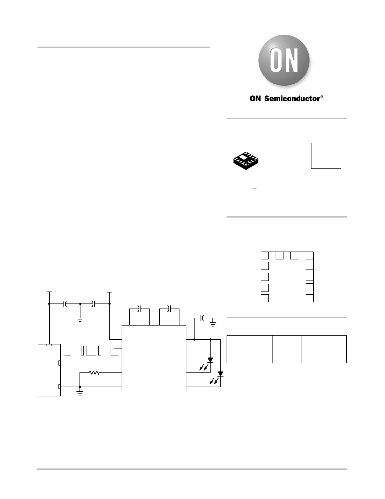
T ypical Applications
• Portable Back Light
• Digital Cellular Phone Camera Photo Flash
• LCD and Key Board Simultaneous Drive
V
CC
C5
1 mF/6.3 V 1 mF/6.3 V
GND
V
CC−cpu
I/O pin
MCU
GND
GND
Figure 1. Typical Single Wire White LED Driver
C3
R1
10k
V
bat
220 nF/10 V
C1
C1N
V
bat
NC
CNTL
I
REF
GND
10
C1P
NCP5612
12
11
6
5
4
1
220 nF/10 V
C2
9
C2N
LED/ICON
U1
8
C2P
V
out
LED1
1 mF/10 V
C4
7
LWY87S
D1
2
3
GND
D2
LWY87S
GND C1N
10
V
bat
C1P
C2N
9
C2P
8
V
7
OUT
LED1
2 12 11
3
LED2
I
4
REF
CNTL
5
NC
6
1
(Top View)
ORDERING INFORMATION
Device Package Shipping†
NCP5612MUTBG LLGA12
(Pb−Free)
†For information on tape and reel specifications,
including part orientation and tape sizes, please
refer to our Tape and Reel Packaging Specification
Brochure, BRD8011/D.
3000/Tape & Ree
© Semiconductor Components Industries, LLC, 2006
August, 2006 − Rev. 0
1 Publication Order Number:
NCP5612/D
Page 2
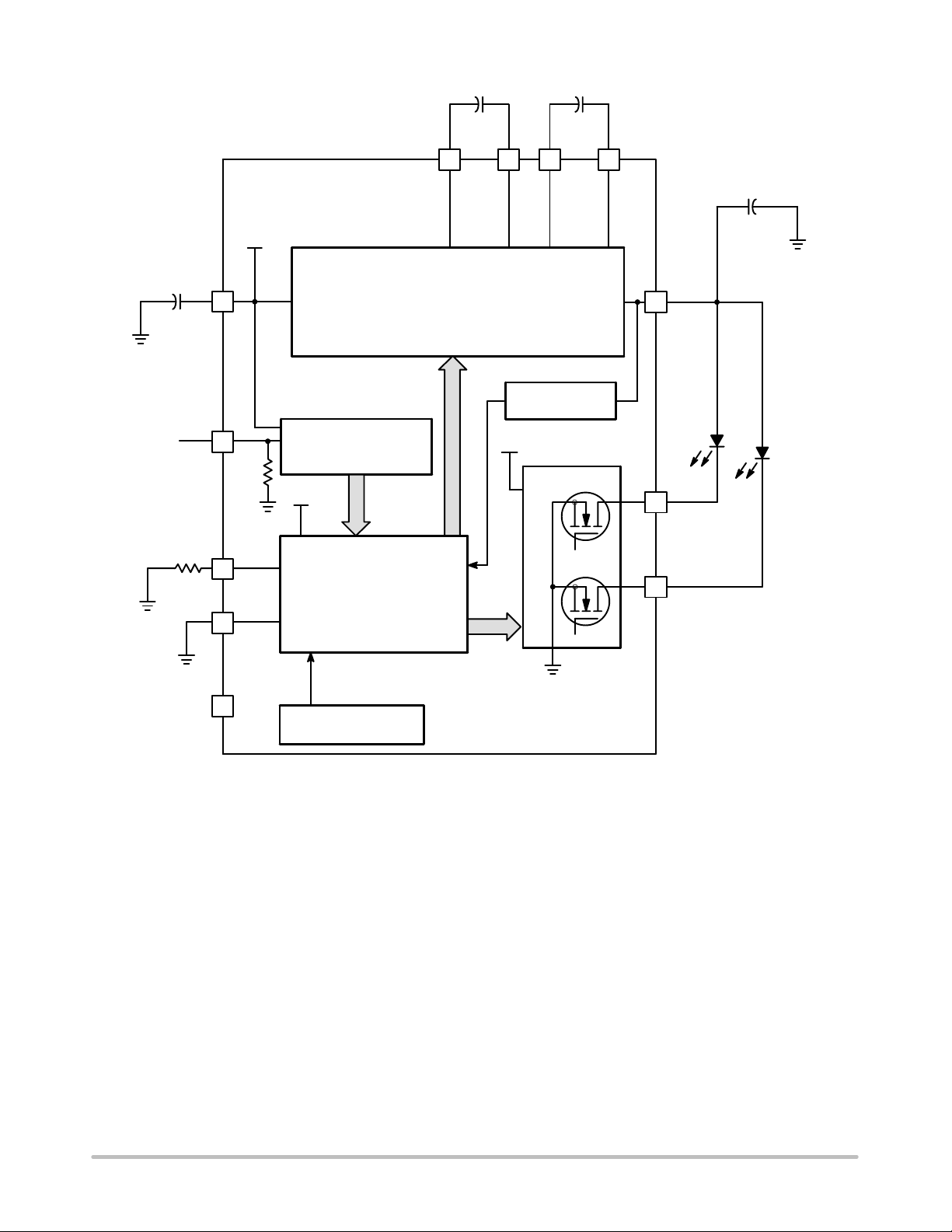
NCP5612
1 mF/6.3 V
GND
C3
CNTL
11
5
V
150 k
bat
DIGITAL CONTROL
V
bat
GND
C1
220 nF 220 nF
12 10
CHARGE PUMP
DC/DC CONVERTER
V
bat
C2
9 8
OVERVOLTAGE
Q1
7
LWY87S
2
C4
1 mF/10 V
GND
V
out
LWY87S
D1
D2
GND
R1
10 k
GND
NC
4
ANALOG CONTROL
1
6
OVERTEMPERATURE
CURRENT MIRRORS
GND
Q2
3
Figure 2. Simplified Block Diagram
http://onsemi.com
2
Page 3
NCP5612
PIN FUNCTION DESCRIPTION
Pin No. Symbol Function Description
1 GND POWER This pin is the GROUND signal for the power analog blocks and must be
2 LED1 INPUT, POWER This pin sinks to ground and monitors the current flowing into the first LED,
3 LED2 INPUT, POWER This pin sinks to ground and monitors the current flowing into the second LED,
4 I
REF
INPUT, ANALOG This pin provides the reference current, based on the internal band−gap
5 CNTL INPUT, DIGITAL This pin supports the flow of data between the external MCU and the
6 NC − No internal connection
7 V
OUT
OUTPUT, POWER This pin provides the output voltage supplied by the DC/DC converter. The
8 C2P POWER One side of the external charge pump capacitor (C
9 C2N POWER One side of the external charge pump capacitor (C
10 C1P POWER One side of the external charge pump capacitor (C
11 V
BAT
INPUT, POWER Input Battery voltage to supply the analog and digital blocks. The pin must be
12 C1N POWER One side of the external charge pump capacitor (C
1. Using low ESR ceramic capacitor, 50 mW maximum, is mandatory to optimize the Charge Pump ef ficiency.
2. Total DC/DC output current is limited to 60 mA.
connected to the system ground. This pin is the GROUND reference for the
DC/DC converter and the output current control. The pin must be connected to
the system ground, a ground plane being strongly recommended.
intended to be used in backlight application. The current is limited to 30 mA
maximum (Note 2).
The LED1 is deactivated when the ICON bit of the LED−REG register is High.
The LED1 is automatically disconnected when an open load is sensed pin 2
during the operation.
intended to be used in backlight application. The current is limited to 30 mA
maximum (Note 2). The LED2 fulfills the ICON function, LED1 being
deactivated, when the ICON bit of the LED−REG register is High.
The LED2 is automatically disconnected when an open load is sensed pin 3
during the operation.
voltage reference, to control the output current flowing in the LED. A 1%
tolerance, or better, resistor shall be used to get the highest accuracy of the
LED biases. An external current source can be used to bias this pin to dim the
light coming out of the LED.
In no case shall the voltage at pin 4 be forced either higher or lower than the
600 mV provided by the internal reference.
NCP5612 internal registers. The protocol makes profit of a Single Wire
structure associated to a Serial 8 bits format data flow.
V
pin must be decoupled to ground by a 1 mF ceramic capacitor located as
out
close as possible to the pin. Cares must be observed to minimize the parasitic
inductance at this pin. The circuit shall not operate without such bypass
capacitor connected across the V
pin and ground.
out
The output voltage is internally clamped to 5.5 V maximum in the event of no
load situation. On the other hand, the output current is limited to 40 mA
(typical) in the event of a short circuit to ground.
) is connected to this
FLY
pin, associated with C2N (Note 1)
) is connected to this
FLY
pin, associated with C2P (Note 1)
) is connected to this
FLY
pin, associated with C1N (Note 1)
decoupled to ground by a 1.0 mF minimum ceramic capacitor.
) is connected to this
FLY
pin, associated with C1P (Note 1)
http://onsemi.com
3
Page 4
NCP5612
MAXIMUM RATINGS
Rating Symbol Value Unit
Power Supply V
BAT
Output Power Supply Vout 7.0 V
Digital Input Voltage
CNTL −0.3 < V < V
Digital Input Current
Human Body Model: R = 1500 W, C = 100 pF (Note 3)
ESD 2.0
Machine Model
LLGA12 Package
Power Dissipation @ TA = +85°C (Note 4)
Thermal Resistance, Junction−to−Case
Thermal Resistance, Junction−to−Air
Operating Ambient Temperature Range T
Operating Junction Temperature Range T
Maximum Junction Temperature T
Storage Temperature Range T
R
R
P
D
q
JC
q
JA
A
J
Jmax
stg
Latch−up Current Maximum Rating per JEDEC Standard: JESD78 − "100 mA
Moisture Sensitivity (Note 5) − 1
Stresses exceeding Maximum Ratings may damage the device. Maximum Ratings are stress ratings only. Functional operation above the
Recommended Operating Conditions is not implied. Extended exposure to stresses above the Recommended Operating Conditions may affect
device reliability.
3. This device series contains ESD protection and exceeds the following tests:
Human Body Model (HBM) "2.0 kV per JEDEC standard: JESD22−A114.
Machine Model (MM) "200 V per JEDEC standard: JESD22−A115.
4. The maximum package power dissipation limit must not be exceeded.
5. Moisture Sensitivity Level (MSL): 1 per IPC/JEDEC standard: J−STD−020A.
7.0 V
BAT
1.0
mA
kV
200
200
51
200
mW
°C/W
°C/W
−40 to +85 °C
−40 to +125 °C
+150 °C
−65 to +150 °C
V
V
POWER SUPPLY SECTION (Typical values are referenced to T
temperature, operating conditions 2.85 V < V
< 5.5 V , unless otherwise noted.)
bat
= +25°C, Min & Max values are referenced −40°C to +85°C ambient
A
Rating Pin Symbol Min Typ Max Unit
Power Supply 11 V
Continuous DC Current in the Load @ Vf = 3.8 V , 3.2 V < V
< 5.5 V , ICON = L
bat
7 I
(30 mA per LED)
Output ICON Current (ICON bit = H) @ 3.2 V < V
< 4.2 V , TA = +25°C 7 I
bat
Continuous Output Short Circuit Current 7 I
Output Voltage Compliance (OVP) 7 V
DC/DC Start Time (C
operation, @ V
Output Voltage T urn−off ( C
V
= 5%
out
Standby Current, 0°C < TA < +85°C
V
= 3.6 V , I
bat
out
Operating Current, @ I
Output LED to LED Current Matching, V
I
= 10 mA, LED1 & LED2 are Identical −25°C < TA < 85°C
LED
Output Current Tolerance @ V
= 1.0 mF) from end of the CNTL T
out
= 3.6 V
bat
= 1 mF) From Last Low Level at CNTL pin to
out
= 0 mA, ICON = L
= 0 mA, ICON = H, V
out
bat
= 3.6 V , I
bat
delay to full load
dst
12 T
12 T
11 I
= 3.6 V 11 I
bat
= 3.6 V ,
= 10 mA −25°C < Ta < 85°C 2, 3 I
LED
2, 3 I
Charge Pump Operating Frequency − F
Thermal Shutdown Protection − T
Thermal Shutdown Protection Hysteresis − T
Efficiency − LED1 = LED2 = 10 mA, Vf = 3.2 V , V
Efficiency − LED1 = LED2 = 30 mA, Vf = 3.75 V , V
= 3.8 V (Total = 20 mA)
bat
= 3.8 V (Total = 60 mA)
bat
−
−
bat
out
ICONTOL
sch
out
start
off
stdb
op
MAT
TOL
pwr
SD
SDH
E
PWR
2.7 − 5.5 V
mA
60 − −
− 450 550 mA
− 40 100 mA
4.8 − 5.7 V
− 150 − ms
− 500 − ms
− − 1.0 mA
− 600 − mA
− "0.2 "1.0 %
− "1.0 − %
− 1.0 − MHz
− 160 − °C
− 30 − °C
−
−
87
84
−
−
%
http://onsemi.com
4
Page 5

NCP5612
ANALOG SECTION (Typical values are referenced to T
temperature, operating conditions 2.85 V < V
< 5.5 V , unless otherwise noted.)
bat
= +25°C, Min & Max values are referenced −40°C to +85°C ambient
A
Rating Pin Symbol Min Typ Max Unit
Reference Current @ V
Reference Voltage (Note 7) 0°C < TA < +85°C 4 V
Base Reference Current (I
= 600 mV (Note 7) 4 I
ref
) Current Ratio − I
REF
REF
REF
LEDR
1.0 − 60 mA
−3% 600 +3% mV
− 500 − −
6. The overall output current tolerance depends upon the accuracy of the external resistor. Using 1% or better resistor is recommended.
7. The external circuit must not force the I
DIGITAL PARAMETERS SECTION (Typical values are referenced to T
ambient temperature, operating conditions 2.85 V < V
ground, Digital inputs overshoot < 0.30 V to V
pin voltage either higher or lower than the 600 mV specified.
REF
= +25°C, Min & Max values are referenced −40°C to +85°C
A
BAT
< 5.5 V , unless otherwise noted.) Note: Digital inputs undershoot < − 0.30 V to
bat
.
Rating Pin Symbol Min Typ Max Unit
Positive going Input High Voltage Threshold, CNTL signals 5 V
Negative going Input Low Voltage Threshold, CNTL signals 5 V
Pull Down Resistor 5 R
Delay between two consecutive frame (Note 9) 5 t
Wake up delay (Note 9) 5 t
CNTL signal rise and fall time (Note 9) 5 tr, t
Clocked CNTL High (Note 9) 5 t
CNTL Low (Note 9) 5 ton, t
CNTL Store data delay (Note 9) 5 T
Input CNTL frequency (Note 9) 5 F
IH
IL
cntl
idle
wkp
f
on
off
dst
CNTL
1.4 − V
BAT
− − 0.6 V
− 150 − kW
10 − − ms
− − 1.0 ms
− − 200 ns
− − 75 ms
1.0 − − ms
− 200 300 ms
− − 400 kHz
8. see Timings Reference
9. Parameter not tested in production, guaranteed by design.
V
http://onsemi.com
5
Page 6

NCP5612
APPLICATION INFORMATION
t
wkp
V
IH
V
IL
VOH @ V
VOH @ V
VOL @ MOTOROLA: 500 mV
VOL @ QUALCOMM: 450 mV
VOL @ INTEL: 400 mV
= 3.0 V 2600 mV
ccio
= 2.6 V 2400 mV
ccio
t
on
Bit = 1 Bit = 0 Bit = 0
t
off
t
f
90%
10%
t
r
90%
Figure 3. Timings Reference
V
1400 mV
IHsw
V
GROUND
IL
600 mV
100 mV/step
Figure 4. Basic Cellular Phone Chip Set Digital Output Levels
DC/DC Operation
The converter is based on a charge pump technique to
generate a DC voltage capable to supply the White LED
load. The system regulates the current flowing into each
LED by means of internal current mirrors associated with
the white diodes. Consequently, the output voltage will be
equal to the Vf of the LED, plus the drop voltage (ranging
from 150 mV to 400 mV, depending upon the output
current and V
/ Vf ratio) developed across the internal
bat
NMOS mirror. Typically, assuming a standard white LED
forward biased at 10 mA, the output voltage will be 3.6 V.
The built−in OVP circuit continuously monitors the
output voltage and stops the converter when the voltage is
above 5.0 V typical. The converter resumes to normal
operation when the voltage drops below the typical 5.0 V
(no latch−up mechanism). Consequently, the chip can
operate with no load during any test procedures.
Load Current Calculation
The load current is derived from the 600 mV reference
voltage provided by the i n t e r n a l B a n d G a p a s s ociated to th e
external resistor connected across I
Figure 5). In any case, no voltage shall be forced at I
pin and Ground (see
REF
REF
pin,
either downward or upward.
The reference current is multiplied by the internal
current mirror, associated to the number of pulses as
depicted Figure 9, to yield the output load current. Since the
reference voltage is based on a temperature compensated
Band Gap, a tight tolerance resistor will provide a very
accurate load current. The resistor is calculated from the
Ohm’s law (R
bias
= V
) and define the maximum
ref/IREF
current flowing into the LED when 20 pulses have been
counted at the CNTL pin.
Since the reference current must be between the
minimum and maximum specified, the resistor value will
range between R
= 300/30 mA = 10 kW and R
bias
bias
=
300/0.5 mA = 600 kW. Obviously, the tolerance of such a
resistor must be 1% or better, with a 100 ppm thermal
coefficient, to get the expected overall tolerance.
Typical applications will run with R
= 10 kW to make
bias
profit of the full dynamic range provided by the S−Wire
DATA byte.
http://onsemi.com
6
Page 7

R1
I
REF
Pin 4
NCP5612
VBandGap
LED Return
Pin 2 & 3
600 mV
GND
GND
Note: the I
pin must never be biased by an external voltage.
REF
Figure 5. Basic Reference Current Source
Load Connection
The NCP5612 is capable to drive the two LED
simultaneously, as depicted (see Figure 1), but the load can
be arranged to accommodate one or two LED if necessary
NCP5612
7
LWY87S
D1
2
3
1 mF/6.3 V
GND
Figure 6. Typical Single and Double LED Connections
Finally, an external network can be connected across V
out
and ground, but the current through such network will not
be regulated by the NCP5612 chip (see Figure 7). On top
of that, the total current out of the V
pin shall be limited
out
to 60 mA.
C4
NCP5612
7
D1
20 mA
2
3
Figure 7. Extra Load Connected to V
GND
LWY87S
LWY87S
20 mA
1uF/6.3V
D3
5mA
D2
R1
220R
LWY87S
LWY87S
D4
5mA
R2
220R
GND
out
in the application (see Figure 6). In this case, the two
current mirrors can be connected in parallel to drive a
single powerful LED, thus yielding 60 mA current
capability in a single LED.
NCP5612
7
LWY87S
D1
2
3
LWY87S
D2
C4
1 mF/6.3 VC4
GND
Single Wire Serial Link Protocol
The proposed S−WIRE uses a pulse count technique
already existing in the data exchange systems. The protocol
supports broken transmission, assuming the hold time is
shorter than the maximum 200 ms typical specified in the
data sheet. The S−WIRE details are provided in the
AND8264 application note.
Based on the two examples provided in Figure 8, the
CNTL pin supports two digital level:
CNTL = Low ³ the system is shut−off and no current
flow in either LED1 or LED2.
CNTL = High ³ the system is active and the two LED
are powered according to the selected sequence.
There is no time delay associated with the Low state and
the LED are switched Off when the CNTL signal drops to
Low. To program a new LED configuration, one shall send
the number of pulses on the CNTL pin according to the true
table:
• The internal counter is reset to zero on the first
negative going transient present on the CNTL pin
http://onsemi.com
7
Page 8

NCP5612
• The first four positive going pulses are used to control
the ICON (LED2):
1. Pulse #1 ³ ICON = 100 mA
2. Pulse #2 ³ ICON = 150 mA
3. Pulse #3 ³ ICON = 250 mA
4. Pulse #4 ³ ICON = 450 mA
• The fifth positive pulse will clear the ICON and
activate the normal operation of LED1 and LED2
• The pulses from the fifth to the twentieth will increase
the LED current according to a pseudo logarithmic
scale (see Figure 9).
• Any pulses beyond the twentieth will not make change
to the LED current if the delay between the pulses is
shorter than 75 ms.
Start Bit
Negative going edge
Clear counter
Example #1: CNTL
LED1= 0 mA
LED2 = ICON
Example #2: CNTL
LED1= 6 mA
LED2 = 6 mA
Example #3: CNTL
LED1= 30 mA
LED2 = 30 mA
Note: timings are not scaled.
Pulse count
ICON = 250 mA
TEHmax 75 ms when clocked
Pulse count
Pulse count
1 23
1234 5 678910
ICON = disabled
1234
ICON = disabled
T
dst
Shut down mode
LED1=LED0= 0 mA
T
EH
LED1=LED2 = 6 mA
5 6789
Figure 8. Basic NCP5612 Programming Sequence
• The system returns to zero if a pulse, delayed by
200Ăms – T
cycle restart from the beginning.
Once the expected LED current value is reached, the
CNTL pin must stay High to store the new data and
maintain the LED active.
The contain of the counter is stored into the internal LED
registers at the end of the built−in 200 ms typical delay: no
action will take place during the end of the last positive
going pulse and the end of the T
prevent the system for broken transmission.
On the other hand, in order to avoid corrupted data
transmission, the High level shall be 75 ms maximum
during a given data frame. Consequently, the pulse
frequency is bounded by a 13 kHz minimum and a 400 kHz
maximum.
T
EL
T
dst
10
11 12 13 14 15 16 17 18 19 20
– , follows the twentieth one and the
dst
delay. Such a protocol
dst
T
dst
LED1=LED2 = 30 mA
LED1=LED2 = 0 mA
http://onsemi.com
8
Page 9

NCP5612
I
(mA)
0
35
DIMMING
The built−in Single Wire Serial Link interface provides
a simple way to accurately control the output current
flowing in the two LED. Provision have been made, at
silicon level, to provide a full dimming of the backlight
(NORMAL mode of operation), the ICON current being
adjustable in four steps when it is activated.
Table 1. LED Dimming Configuration
Pulse Count LED activity
Pulse 1 LED#2 = 100 mA, LED#1 de−activated
Pulse 2 LED#2 = 150 mA, LED#1 de−activated
Pulse 3 LED#2 = 250 mA, LED#1 de−activated
Pulse 4 LED#2 = 450 mA, LED#1 de−activated
Pulse 5 to Pulse 20 ICON de−activated, NORMAL back-
light takes place
The DC/DC converter is switched OFF and the two LED
are disconnected when LED−REG=$00.
When the ICON mode is activated, the DC/DC converter
is switched OFF, LED#1 is deactivated from the LED
current sense and the programmed bias current (powered
from the V
source) is forced into LED#2.
bat
Bit Clock I−LED(mA) Bit Clock I−LED(mA)
1 1
2 2 10 14
3 3 11 16
4 4 12 19
5 5 13 22
6 6 14 25
7 8 15 28
8 10 16 31
I
= F(Bit Clock)
30
25
20
15
OUT
10
5.0
OUT
(linear scale)
0
BIT CLOCK
9 12
15105.00
Figure 9. Typical Output Current Slope
2
Figure 10. Typical Efficiency
http://onsemi.com
9
Page 10

NCP5612
J1
2
1
POWER
GND
V
BAT
GND
J2
12
34
56
78
9
10
S−WIRE PORT
TP1
DATA
Figure 11. Typical LED to LED Current Matching
C1
4.7 mF/10 V
220 nF/6.3 V
220 nF/6.3 V
GND
IREFBK
R1
DATA
C2
10
12
C1P
C1N
11
V
bat
6
NC
CNTL
I
REF
GND
NCP5612
5
4
1
9
C2N
U1
LED/ICON
C3
C2P
V
out
LED1
8
7
2
3
10 k
Z1
GND
GND
Figure 12. Demo Board Schematic Diagram
V
OUT
LED1
LED2
D1
GND
C4
1.0 mF/10 V
LWY87S
D2LWY87S
TP2
V
OUT
http://onsemi.com
10
Page 11
NCP5612
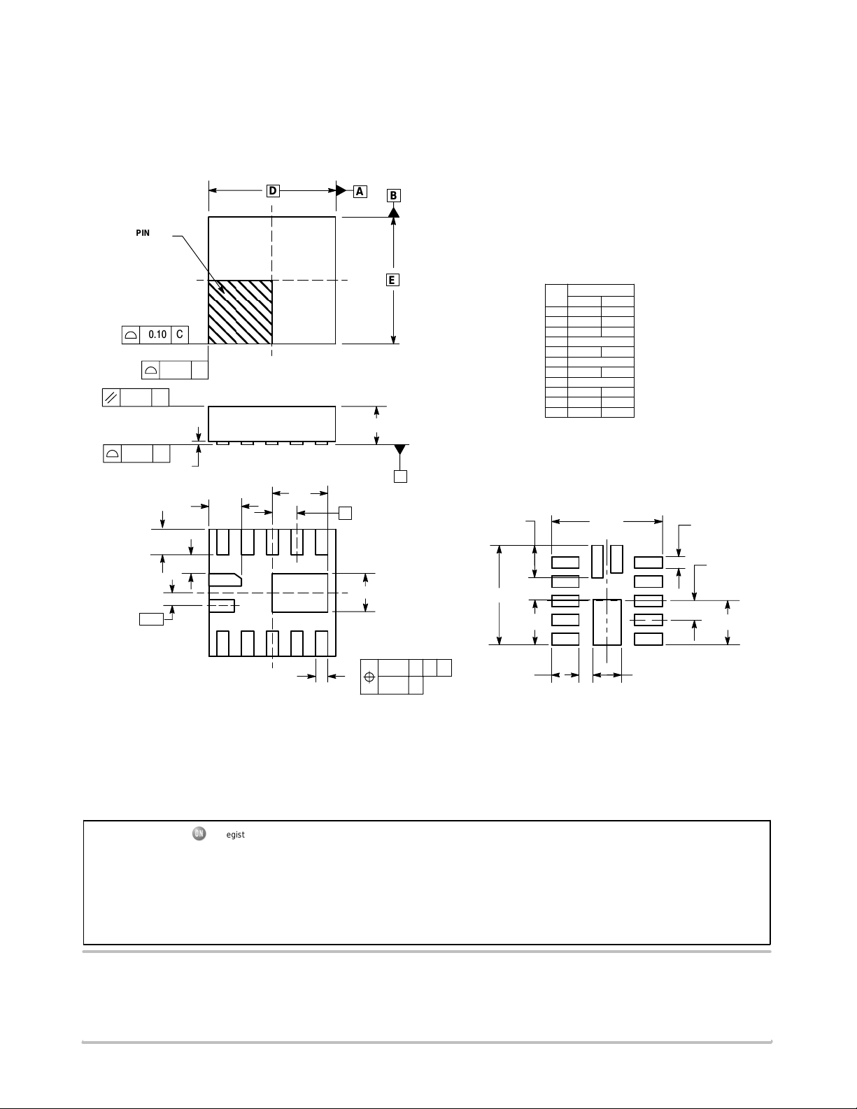
PACKAGE DIMENSIONS
LLGA12
MU SUFFIX
CASE 513AA−01
ISSUE O
12X
REFERENCE
2 X
SEATING
PLANE
PIN ONE
2 X
C0.10
C0.08
11X
e/2
D
C0.10
C0.10
TOP VIEW
A
B
E
NOTES:
1. DIMENSIONING AND TOLERANCING PER
ASME Y14.5M, 1994 .
2. CONTROLLING DIMENSION: MILLIMETERS.
3. DIMENSION b APPLIES TO PLATED
TERMINAL AND IS MEASURED BETWEEN
0.15 AND 0.20 MM FROM TERMINAL.
4. COPLANARITY APPLIES TO THE EXPOSED
PAD AS WELL AS THE TERMINALS.
MILLIMETERS
DIM MIN MAX
A 0.50 0.60
A1 0.00 0.05
b 0.15 0.25
D 2.00 BSC
D2 0.80 1.00
E 2.00 BSC
E2 0.55 0.65
e 0.40 BSC
K 0.25 −−−
L 0.30 0.50
L1 0.40 0.60
A
L1
2
SIDE VIEW
D2
C
SOLDERING FOOTPRINT*
9X
e
6
E2
2.06
0.66
2.30
1
0.93
12X
0.23
0.40
PITCH
0.91
A1
L
K
1
12
11
BOTTOM VIEW
7
12X
0.10 C
0.05 C
A BB
NOTE 3
b
11X
0.630.56
DIMENSIONS: MILLIMETERS
*For additional information on our Pb−Free strategy and soldering
details, please download the ON Semiconductor Soldering and
Mounting Techniques Reference Manual, SOLDERRM/D.
ON Semiconductor and are registered trademarks of Semiconductor Components Industries, LLC (SCILLC). SCILLC reserves the right to make changes without further notice
to any products herein. SCILLC makes no warranty, representation or guarantee regarding the suitability of its products for any particular purpose, nor does SCILLC assume any
liability arising out of the application or use of any product or circuit, and specifically disclaims any and all liability, including without limitation special, consequential or incidental
damages. “Typical” parameters which may be provided in SCILLC data sheets and/or specifications can and do vary in different applications and actual performance may vary over
time. All operating parameters, including “Typicals” must be validated for each customer application by customer’s technical experts. SCILLC does not convey any license under
its patent rights nor the rights of others. SCILLC products are not designed, intended, or authorized for use as components in systems intended for surgical implant into the body,
or other applications intended to support or sustain life, or for any other application in which the failure of the SCILLC product could create a situation where personal injury or death
may occur. Should Buyer purchase or use SCILLC products for any such unintended or unauthorized application, Buyer shall indemnify and hold SCILLC and its officers, employees,
subsidiaries, affiliates, and distributors harmless against all claims, costs, damages, and expenses, and reasonable attorney fees arising out of, directly or indirectly, any claim of
personal injury or death associated with such unintended or unauthorized use, even if such claim alleges that SCILLC was negligent regarding the design or manufacture of the part.
SCILLC is an Equal Opportunity/Affirmative Action Employer. This literature is subject to all applicable copyright laws and is not for resale in any manner.
PUBLICATION ORDERING INFORMATION
LITERATURE FULFILLMENT:
Literature Distribution Center for ON Semiconductor
P.O. Box 5163, Denver, Colorado 80217 USA
Phone: 303−675−2175 or 800−344−3860 Toll Free USA/Canada
Fax: 303−675−2176 or 800−344−3867 Toll Free USA/Canada
Email: orderlit@onsemi.com
N. American Technical Support: 800−282−9855 Toll Free
USA/Canada
Europe, Middle East and Africa Technical Support:
Phone: 421 33 790 2910
Japan Customer Focus Center
Phone: 81−3−5773−3850
http://onsemi.com
ON Semiconductor Website: www.onsemi.com
Order Literature: http://www.onsemi.com/orderlit
For additional information, please contact your local
Sales Representative
NCP5612/D
11
 Loading...