

NCP3063, NCP3063B,
NCV3063
1.5 A, Step-Up/Down/
Inverting Switching
Regulators
The NCP3063 Series is a higher frequency upgrade to the popular
MC34063A and MC33063A monolithic DC-DC converters. These
devices consist of an internal temperature compensated reference,
comparator, a controlled duty cycle oscillator with an active current
limit circuit, a driver and a high current output switch. This series was
specifically designed to be incorporated in Step-Down, Step-Up and
Voltage-Inverting applications with a minimum number of external
components.
Features
•Operation to 40 V Input
•Low Standby Current
•Output Switch Current to 1.5 A
•Output Voltage Adjustable
•Frequency Operation of 150 kHz
•Precision 1.5% Reference
•New Features: Internal Thermal Shutdown with Hysteresis
New Features: Cycle-by-Cycle Current Limiting
•Pb-Free Packages are Available
Applications
•Step-Down, Step-Up and Inverting supply applications
•High Power LED Lighting
•Battery Chargers
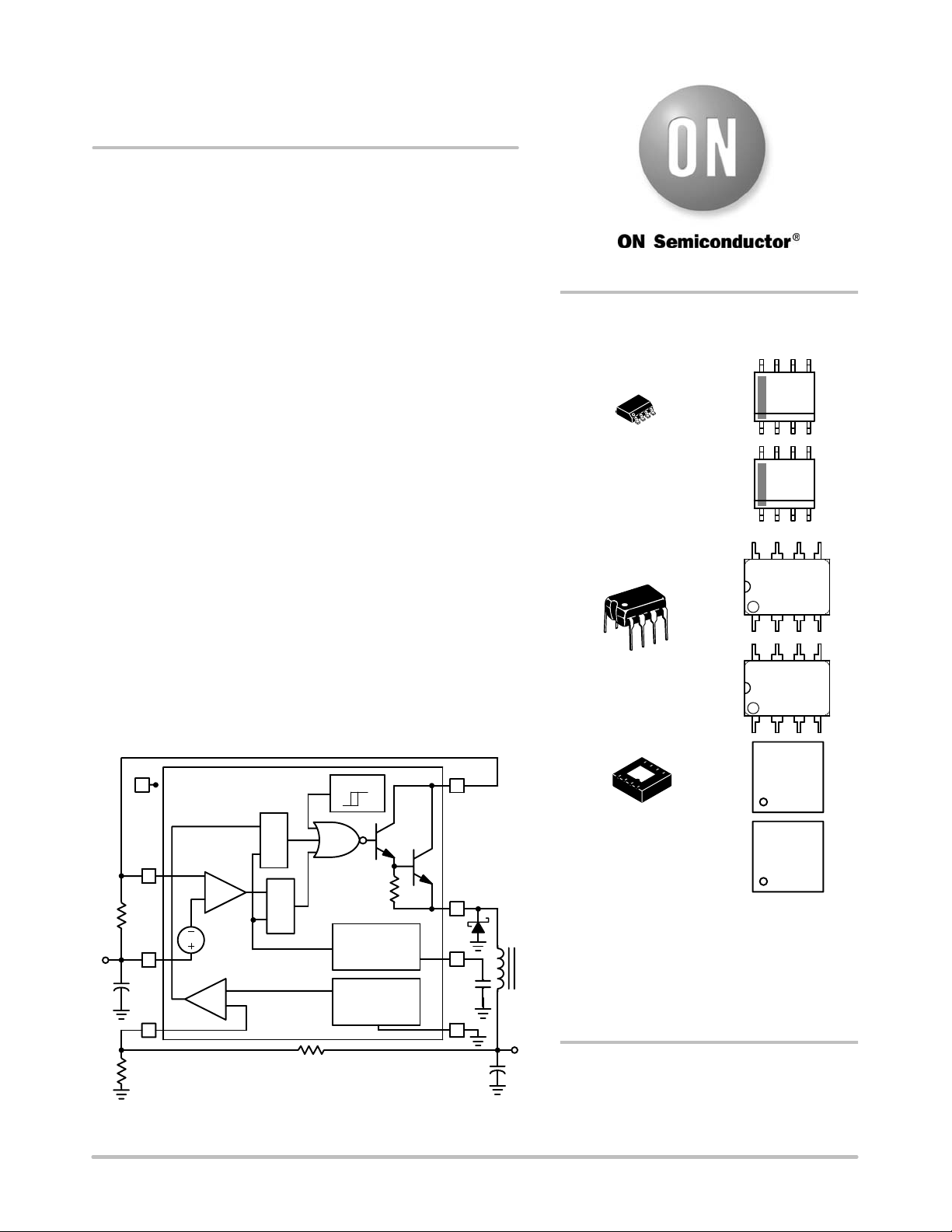
V
in
12 V
8
Rs
0.15 W
+
C
in
220 mF
R1
2.4 kW
7
COMPARATOR
6
5
+
0.2 V
+
-
NCP3063
SET dominant
R
Q
S
S
Q
R
COMPARATOR
R2
SET dominant
REFERENCE
REGULATOR
3.9 kW
Figure 1. Typical Buck Application Circuit
TSD
OSCILLATOR
CT
1.25 V
1
2
D
3
CT
2.2 nF
4
470 mF
V
out
3.3 V /
800 mA
+
C
out
L
47 mH
http://onsemi.com
MARKING
DIAGRAMS
3063x
8
1
SOIC-8
D SUFFIX
CASE 751
8
1
PDIP-8
P, P1 SUFFIX
CASE 626
8
1
DFN-8
SUFFIX
CASE 488
NCP3063x = Specific Device Code
x = B
A = Assembly Location
L, WL = Wafer Lot
Y, YY = Year
W, WW = Work Week
G = Pb-Free Package
(Note: Microdot may be in either location)
ALYW
G
1
V3063
ALYW
G
1
NCP3063x
AWL
YYWWG
1
NCV3063
AWL
YYWWG
1
NCP
3063x
ALYW
G
NCV
3063
ALYW
G
ORDERING INFORMATION
See detailed ordering and shipping information in the package
dimensions section on page 16 of this data sheet.
© Semiconductor Components Industries, LLC, 2007
June, 2007 - Rev. 3
1 Publication Order Number:
NCP3063/D
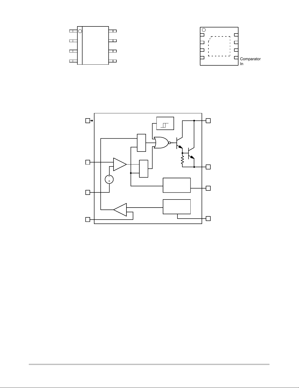
NCP3063, NCP3063B, NCV3063
Switch Collector
Switch Emitter
Timing Capacitor
GND
Figure 2. Pin Connections
N.C.
Ipk Sense
+V
CC
Comparator Inverting Input
1
2
3
4
(Top View)
8
7
6
5
N.C.
Ipk Sense
V
CC
Comparator
Inverting
Input
Switch Collector
Switch Emitter
Timing Capacitor
GND
NOTE: EP Flag must be tied to GND Pin 4
on PCB
EP Flag
(Top View)
N.C.
Ipk Sense
V
CC
Comparator
Inverting
Input
Figure 3. Pin Connections
NCP3063
8
SET dominant
R
Q
S
7
6
5
COMPARATOR
+
0.2 V
COMPARATOR
+
-
S
Q
R
TSD
SET dominant
OSCILLATOR
CT
1.25 V
REFERENCE
REGULATOR
1
Switch Collector
2
Switch Emitter
3
Timing Capacitor
4
GND
Figure 4. Block Diagram
http://onsemi.com
2
NCP3063, NCP3063B, NCV3063
PIN DESCRIPTION
Pin No. Pin Name Description
1 Switch Collector Internal Darlington switch collector
2 Switch Emitter Internal Darlington switch emitter
3 Timing Capacitor
Oscillator Input
4 GND Ground pin for all internal circuits
5 Comparator
Inverting Input
6 V
CC
7 Ipk Sense Peak Current Sense Input to monitor the voltage drop across an external resistor to limit the peak
8 N.C. Pin Not Connected
Exposed
Exposed Pad The exposed pad beneath the package must be connected to GND (Pin 4). Additionally, using
Pad
MAXIMUM RATINGS (measured vs. Pin 4, unless otherwise noted)
VCC pin 6 V
Comparator Inverting Input pin 5 V
Darlington Switch Collector pin 1 V
Darlington Switch Emitter pin 2 (transistor OFF) V
Darlington Switch Collector to Emitter pin 1-2 V
Darlington Switch Current I
Ipk Sense Pin 7 V
Timing Capacitor Pin 3 V
POWER DISSIPATION AND THERMAL CHARACTERISTICS
PDIP-8
Thermal Resistance Junction-to-Air
SOIC-8
Thermal Resistance Junction-to-Air
DFN-8
Thermal Resistance Junction-to-Air
Storage Temperature Range T
Maximum Junction Temperature
Operating Junction Temperature Range (Note 3)
NCP3063
NCP3063B, NCV3063
Stresses exceeding Maximum Ratings may damage the device. Maximum Ratings are stress ratings only. Functional operation above the
Recommended Operating Conditions is not implied. Extended exposure to stresses above the Recommended Operating Conditions may affect
device reliability.
1. This device series contains ESD protection and exceeds the following tests:
Pin 1-8: Human Body Model 2000 V per AEC Q100-002; 003 or JESD22/A114; A115
Machine Model Method 200 V
2. This device contains latch-up protection and exceeds 100 mA per JEDEC Standard JESD78.
3. The relation between junction temperature, ambient temperature and Total Power dissipated in IC is TJ = TA + R
4. The pins which are not defined may not be loaded by external signals
Timing Capacitor
Inverting input pin of internal comparator
Voltage Supply
current through the circuit
proper layout techniques, the exposed pad can greatly enhance the power dissipation capabilities
of the NCP3063.
Rating Symbol Value Unit
CC
CII
SWC
SWE
SWCE
SW
IPK
TCAP
0 to +40 V
-0.2 to + V
CC
0 to +40 V
-0.6 to + V
CC
0 to +40 V
1.5 A
-0.2 to VCC + 0.2 V
-0.2 to +1.4 V
V
V
Rating Symbol Value Unit
°C/W
R
q
JA
100
°C/W
R
q
JA
180
°C/W
R
T
J MAX
q
STG
T
JA
J
80
-65 to +150 °C
+150 °C
°C
0 to +70
-40 to +125
P
q •
D
http://onsemi.com
3
NCP3063, NCP3063B, NCV3063
ELECTRICAL CHARACTERISTICS (V
= 5.0 V, T
CC
= T
J
low
to T
[Note 5], unless otherwise specified)
high
Symbol Characteristic Conditions Min Typ Max Unit
OSCILLATOR
f
OSC
I
DISCHG
I
CHG
I
DISCHG
I
CHG
V
IPK(Sense)
Frequency (V
/
Discharge to Charge Current Ratio (Pin 7 to VCC, TJ = 25°C) 5.5 6.0 6.5 -
5 = 0 V, CT = 2.2 nF,
Pin
= 25°C)
T
J
110 150 190 kHz
Capacitor Discharging Current (Pin 7 to VCC, TJ = 25°C) 1650
Capacitor Charging Current (Pin 7 to VCC, TJ = 25°C) 275
Current Limit Sense Voltage (TJ = 25°C) (Note 6) 165 200 235 mV
OUTPUT SWITCH (Note 7)
V
SWCE(DROP)
I
C(OFF)
Darlington Switch Collector to
Emitter Voltage Drop
(ISW = 1.0 A, Pin 2 to GND,
TJ = 25°C) (Note 7)
1.0 1.3 V
Collector Off-State Current (VCE = 40 V) 0.01 100
COMPARATOR
V
TH
Threshold Voltage
TJ = 25°C 1.250 V
NCP3063 -1.5 +1.5 %
NCP3063B, NCV3063 -2 +2 %
REG
I
CII in
Threshold Voltage Line Regulation (VCC = 5.0 V to 40 V) -6.0 2.0 6.0 mV
LiNE
Input Bias Current (Vin = Vth) -1000 -100 1000 nA
TOTAL DEVICE
I
CC
Supply Current (VCC = 5.0 V to 40 V,
CT = 2.2 nF, Pin 7 = VCC,
V
5 > Vth, Pin 2 = GND,
Pin
remaining pins open)
7.0 mA
Thermal Shutdown Threshold 160 °C
Hysteresis 10 °C
5. NCP3063: T
NCP3063B, NCV3063: T
6. The V
IPK(Sense)
on comparator response time and di/dt current slope. See the Operating Description section for details.
= 0°C, T
low
Current Limit Sense Voltage is specified at static conditions. In dynamic operation the sensed current turn-off value depends
= +70°C;
high
= -40°C, T
low
= +125°C
high
7. Low duty cycle pulse techniques are used during test to maintain junction temperature as close to ambient temperature as possible.
8. NCV prefix is for automotive and other applications requiring site and change control.
mA
mA
mA
http://onsemi.com
4
NCP3063, NCP3063B, NCV3063
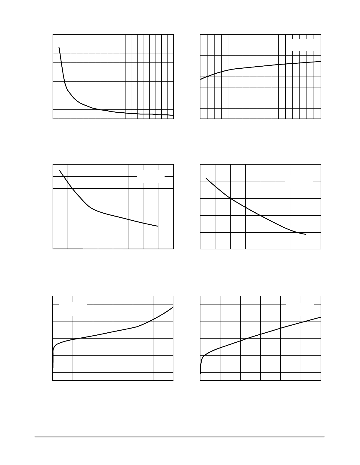
450
400
350
300
250
200
150
FREQUENCY (kHz)
100
50
0
0 1 2 3 4 5 6 7 8 9 101112 13 14 15161718 1920
Ct, CAPACITANCE (nF) VCC, SUPPLY VOLTAGE (V)
Figure 5. Oscillator Frequency vs. Oscillator
Timing Capacitor
2.4
2.2
2.0
1.8
VCC = 5.0 V
IE = 1 A
190
180
170
160
150
140
FREQUENCY (Hz)
130
120
110
Figure 6. Oscillator Frequency vs. Supply
1.25
1.20
1.15
CT = 2.2 nF
TJ = 25°C
21 34 38
Voltage
VCC = 5.0 V
IC = 1 A
402925161273
1.6
1.4
VOLTAGE DROP (V)
1.2
1.0
TJ, JUNCTION TEMPERATURE (°C) TJ, JUNCTION TEMPERATURE (°C)
Figure 7. Emitter Follower Configuration Output
Darlington Switch Voltage Drop vs. Temperature
2.0
1.9
VCC = 5.0 V
TJ = 25°C
1.8
1.7
1.6
1.5
1.4
1.3
VOLTAGE DROP (V)
1.2
1.1
1.0
IE, EMITTER CURRENT (A) IC, COLLECTOR CURRENT (A)
Figure 9. Emitter Follower Configuration Output
Darlington Switch Voltage Drop vs. Emitter Current
1.10
VOLTAGE DROP (V)
1.05
150100500-50
1.0
150100500-50
Figure 8. Common Emitter Configuration Output
Darlington Switch Voltage Drop vs. Temperature
1.5
1.4
1.3
1.2
1.1
1.0
0.9
0.8
VOLTAGE DROP (V)
0.7
0.6
1.51.00.50
0.5
VCC = 5.0 V
TJ = 25°C
1.51.00.50
Figure 10. Common Emitter Configuration
Output Darlington Switch Voltage Drop vs.
Collector Current
http://onsemi.com
5
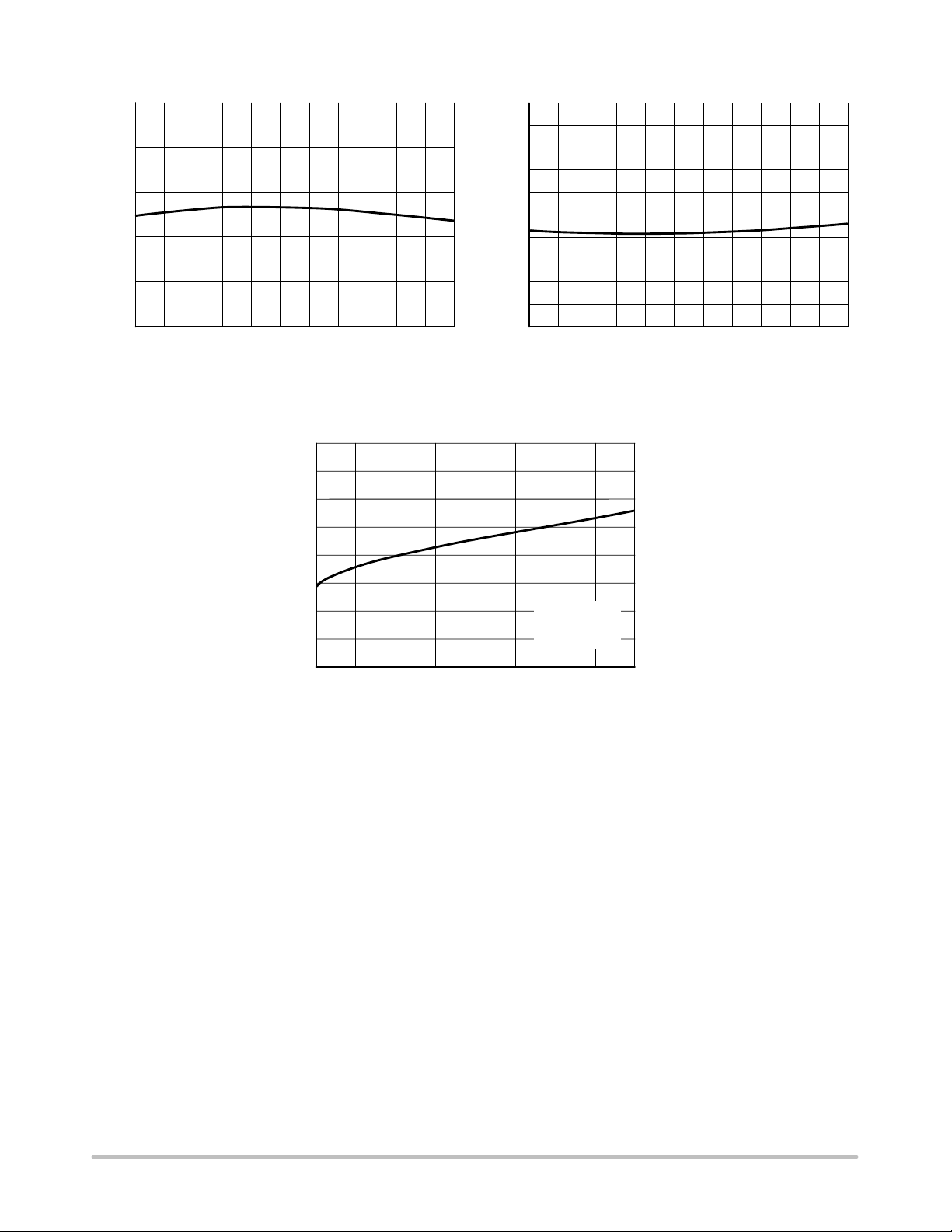
NCP3063, NCP3063B, NCV3063
1.30
1.28
1.26
1.24
1.22
1.20
, COMPARATOR THRESHOLD VOLTAGE (V)
th
V
0.30
0.28
0.26
0.24
0.22
0.20
0.18
VOLTAGE (V)
, CURRENT LIMIT SENSE
0.16
0.14
ipk(sense)
0.12
V
-10 806550 110
TJ, JUNCTION TEMPERATURE (°C) TJ, JUNCTION TEMPERATURE (°C)
1259535205-25-40
Figure 11. Comparator Threshold Voltage vs.
Temperature
6.0
5.5
5.0
4.5
0.10
20 95 110
Figure 12. Current Limit Sense Voltage vs.
Temperature
65 80
12550355-10-25-40
4.0
3.5
3.0
, SUPPLY CURRENT (mA)
CC
I
2.5
2.0
13 18 23 43
VCC, SUPPLY VOLTAGE (V)
CT = 2.2 nF
Pin 5, 7 = V
Pin 2 = GND
3833288.03.0
CC
Figure 13. Standby Supply Current vs. Supply Voltage
http://onsemi.com
6

NCP3063, NCP3063B, NCV3063
INTRODUCTION
The NCP3063 is a monolithic power switching regulator
optimized for dc to dc converter applications. The
combination of its features enables the system designer to
directly implement step-up, step-down, and voltageinverting converters with a minimum number of external
components. Potential applications include cost sensitive
consumer products as well as equipment for industrial
markets. A representative block diagram is shown in
Figure4.
controlled by the oscillator, thus pumping up the output filter
capacitor. When the output voltage level reaches nominal,
the output switch next cycle turning on is inhibited. The
feedback comparator will enable the switching immediately
when the load current causes the output voltage to fall below
nominal. Under these conditions, output switch conduction
can be enabled for a partial oscillator cycle, a partial cycle
plus a complete cycle, multiple cycles, or a partial cycle plus
multiple cycles. (See AN920/D for more information).
Operating Description
The NCP3063 is a hysteric, dc-dc converter that uses a
gated oscillator to regulate output voltage. In general, this
mode of operation is somewhat analogous to a capacitor
charge pump and does not require dominant pole loop
compensation for converter stability. The Typical Operating
Waveforms are shown in Figure 14. The output voltage
waveform shown is for a step-down converter with the
ripple and phasing exaggerated for clarity. During initial
converter startup, the feedback comparator senses that the
output voltage level is below nominal. This causes the
output switch to turn on and off at a frequency and duty cycle
Feedback Comparator Output
IPK Comparator Output
Timing Capacitor, C
1
0
1
0
T
Oscillator
The oscillator frequency and off-time of the output switch
are programmed by the value selected for timing capacitor
CT. Capacitor CT is charged and discharged by a 1 to 6 ratio
internal current source and sink, generating a positive going
sawtooth waveform at Pin 3. This ratio sets the maximum
tON/(tON + t
) of the switching converter as 6/(6 + 1) or
OFF
0.857 (typical) The oscillator peak and valley voltage
difference is 500 mV typically. To calculate the CT capacitor
value for required oscillator frequency, use the equations
found in Figure 15. An Excel based design tool can be found
at www.onsemi.com on the NCP3063 product page.
Output Switch
On
Off
Nominal Output Voltage Level
Output Voltage
Startup Operation
Figure 14. Typical Operating Waveforms
http://onsemi.com
7

NCP3063, NCP3063B, NCV3063
Peak Current Sense Comparator
With a voltage ripple gated converter operating under
normal conditions, output switch conduction is initiated by
the Voltage Feedback comparator and terminated by the
oscillator. Abnormal operating conditions occur when the
converter output is overloaded or when feedback voltage
sensing is lost. Under these conditions, the Ipk Current Sense
comparator will protect the Darlington output Switch. The
switch current is converted to a voltage by inserting a
fractional ohm resistor, RSC, in series with VCC and the
Darlington output switch. The voltage drop across RSC is
monitored by the Current Sense comparator. If the voltage
drop exceeds 200 mV with respect to VCC, the comparator
will set the latch and terminate output switch conduction on
a cycle-by-cycle basis. This Comparator/Latch
configuration ensures that the Output Switch has only a
single on-time during a given oscillator cycle.
Real
V
on
turn- off
Rs Resistor
di/dt slope
V
ipk(sense)
The V
IPK(Sense)
Io
t_delay
Current Limit Sense Voltage threshold is
specified at static conditions. In dynamic operation the
sensed current turn-off value depends on comparator
response time and di/dt current slope.
I1
I through the
Darlington
Switch
Real V
V
turn_off
turn- off
+ V
on Rsc resistor
ipk(sense)
) Rs @ (t_delay @ dińdt)
Typical Ipk comparator response time t_delay is 350 ns.
The di/dt current slope is growing with voltage difference on
the inductor pins and with decreasing inductor value.
It is recommended to check the real max peak current in
the application at worst conditions to be sure that the max
peak current will never get over the 1.5A Darlington Switch
Current max rating.
Thermal Shutdown
Internal thermal shutdown circuitry is provided to protect
the IC in the event that the maximum junction temperature
is exceeded. When activated, typically at 160°C, the Output
Switch is disabled. The temperature sensing circuit is
designed with 10°C hysteresis. The Switch is enabled again
when the chip temperature decreases to at least 150°C
threshold. This feature is provided to prevent
catastrophic failures from accidental device
overheating. It is not intended to be used as a
replacement for proper heatsinking.
Output Switch
The output switch is designed in a Darlington
configuration. This allows the application designer to
operate at all conditions at high switching speed and low
voltage drop. The Darlington Output Switch is designed to
switch a maximum of 40 V collector to emitter voltage and
current up to 1.5 A.
APPLICATIONS
Figures 16 through 24 show the simplicity and flexibility
of the NCP3063. Three main converter topologies are
demonstrated with actual test data shown below each of the
circuit diagrams.
Figure 15 gives the relevant design equations for the key
parameters. Additionally, a complete application design aid
for the NCP3063 can be found at www.onsemi.com.
Figures 25 through 31 show typical NCP3063
applications with external transistors. This solution helps to
increase output current and helps with efficiency still
keeping low cost bill of materials. Typical schematics of
boost configuration with NMOS transistor, buck
configuration with PMOS transistor and buck configuration
with LOW V
PNP are shown.
CE(sat)
Another advantage of using the external transistor is
higher operating frequency which can go up to 250 kHz.
Smaller size of the output components such as inductor and
capacitor can be used then.
http://onsemi.com
8

NCP3063, NCP3063B, NCV3063
(See Notes 9, 10, 11) Step-Down Step-Up Voltage-Inverting
|V
t
on
t
off
t
on
C
T
I
L(avg)
I
pk (Switch)
R
SC
L
V
ripple(pp)
V
out
9. V
10.VF - Output rectifier forward voltage drop. Typical value for 1N5819 Schottky barrier rectifier is 0.4 V.
11.The calculated ton/t
The Following Converter Characteristics Must Be Chosen:
- Darlington Switch Collector to Emitter Voltage Drop, refer to Figures 7, 8, 9 and 10.
SWCE
Vin* V
ǒ
DI
must not exceed the minimum guaranteed oscillator charge to discharge ratio.
off
Vin* V
I
L(avg)
Ǹ
ǒ
L
V
V
) V
out
SWCE
t
on
t
off
t
on
ǒ
f
) 1
t
off
I
out
)
0.20
I
pk(Switch)
* V
SWCE
DI
L
2
1
Ǔ
8fC
O
R
2
ǒ
TH
) 1
R
1
F
* V
out
Ǔ
DI
L
2
out
Ǔ
) (ESR)
Ǔ
V
) VF* V
out
Vin* V
t
t
t
on
ǒ
f
t
off
f
osc
I
out
I
L(avg)
I
pk(Switch)
Vin* V
DI
t
onIout
C
O
V
TH
*6
t
on
ǒ
t
off
0.20
SWCE
L
) DIL@ ESR [
R
ǒ
R
381.6 @ 10
CT+
t
on
2
ǒ
[
in
SWCE
on
off
Ǔ
) 1
* 343 @ 10
Ǔ
) 1
DI
L
)
2
Ǔ
t
2
Ǔ
) 1
1
on
*12
Vin* V
ǒ
t
onIout
Vin - Nominal operating input voltage.
V
- Desired output voltage.
out
I
- Desired output current.
out
DIL - Desired peak-to-peak inductor ripple current. For maximum output current it is suggested that DIL be chosen to be
less than 10% of the average inductor current I
set by RSC. If the design goal is to use a minimum inductance value, let DIL = 2(I
. This will help prevent I
L(avg)
pk (Switch)
from reaching the current limit threshold
). This will proportionally reduce
L(avg)
converter output current capability.
f - Maximum output switch frequency.
V
ripple(pp)
- Desired peak-to-peak output ripple voltage. For best performance the ripple voltage should be kept to a low
value since it will directly affect line and load regulation. Capacitor CO should be a low equivalent series resistance (ESR)
electrolytic designed for switching regulator applications.
| ) V
out
Vin* V
t
on
t
off
t
on
ǒ
f
t
off
t
on
ǒ
I
out
t
off
I
L(avg)
0.20
I
pk(Switch)
SWCE
DI
L
) DIL@ ESR
C
O
R
ǒ
V
TH
R
SWCE
Ǔ
) 1
) 1
DI
)
2
) 1
1
F
Ǔ
L
2
Ǔ
t
on
Ǔ
Figure 15. Design Equations
http://onsemi.com
9

NCP3063, NCP3063B, NCV3063
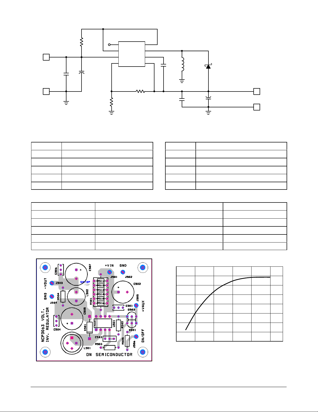
R201
0R15
+VIN = +12 V
1
J201
C201
0.1 mF
+
C202
220 mF / 50 V
J202
1
GND
Value of Components
Name Value
L201
D201 1 A, 40 V Schottky Rectifier
C202
C205
C203 2.2 nF Ceramic Capacitor
47 mH, I
> 1.5 A
sat
220 mF, 50 V, Low ESR
470 mF, 25 V, Low ESR
U201
8
N.C. SWC
7
I
PK
V
CC
5
COMP
NCP3063
SWE
TCAP
GND
1
2
36
4
C203
2.2 nF
L201
D201
1N5819
47 mH
C206
0.1 mF
R203
R202
3K9 ±1%
2K4 ±1%
Figure 16. Typical Buck Application Schematic
Name Value
R201
R202
R203
C201 100 nF Ceramic Capacitor
C202 100 nF Ceramic Capacitor
150 mW, 0.5 W
2.40 kW
3.90 kW
+V
OUT
+
C205
470 mF / 25 V
= +3.3 V / 800 mA
1
J203
J204
1
GND
Test Results
Test Condition Results
Line Regulation Vin = 9 V to 12 V, Io = 800 mA 8 mV
Load Regulation Vin = 12 V, Io = 80 mA to 800 mA 9 mV
Output Ripple Vin = 12 V, Io = 40 mA to 800 mA ≤ 85 mV
Efficiency Vin = 12 V, Io = 400 mA to 800 mA > 73%
Short Circuit Current
Vin = 12 V, R
= 0.15 W
load
1.25 A
76
74
72
70
68
EFFICIENCY (%)
66
64
0.1 0.2 0.3 0.4 0.5 0.6 0.7 0.8 0.9 1.0
OUTPUT LOAD (Adc)
Figure 18. Efficiency vs. Output Current for the Buck
Figure 17. Buck Demoboard Layout
Demo Board at V
= 12 V, V
in
pp
= 3.3 V, T
out
= 255C
A
http://onsemi.com
10

NCP3063, NCP3063B, NCV3063
R101
+VIN = +12 V
1
J101
C101
0.1 mF
J102
1
GND
0R15
+
C102
470 mF / 25 V
Value of Components
Name Value
L101
D101 1 A, 40 V Schottky Rectifier
C102
C105
C103 2.2 nF Ceramic Capacitor
100 mH, I
470 mF, 25 V, Low ESR
330 mF, 50 V, Low ESR
> 1.5 A
sat
L101
8
7
5
R102
1K0 ±1%
100 mH
U101
N.C. SWC
SWE
I
PK
TCAP
V
CC
COMP
GND
NCP3063
1
2
36
4
R103
18K0 ±1%
D101 1N5819
C103
2.2 nF
C106
0.1 mF
Figure 19. Typical Boost Application Schematic
Name Value
R101
R102
R103
C101 100 nF Ceramic Capacitor
C106 100 nF Ceramic Capacitor
150 mW, 0.5 W
1.00 kW
18.00 kW
+V
+
C105
330 mF / 50 V
= +24 V / 350 mA
OUT
1
J103
J104
1
GND
Test Results
Test Condition Results
Line Regulation Vin = 9 V to 15 V, Io = 250 mA 2 mV
Load Regulation Vin = 12 V, Io = 30 mA to 350 mA 5 mV
Output Ripple Vin = 12 V, Io = 10 mA to 350 mA ≤ 350 mV
Efficiency Vin = 12 V, Io = 50 mA to 350 mA > 85.5%
90
89
88
87
86
85
84
EFFICIENCY (%)
83
82
81
80
0 0.05 0.1 0.15 0.2 0.3 0.4
OUTPUT LOAD (Adc)
0.25 0.35
Figure 21. Efficiency vs. Output Current for the Boost
Figure 20. Boost Demoboard Layout
Demo Board at V
= 12 V, V
in
out
pp
= 24 V, T
= 255C
A
http://onsemi.com
11
NCP3063, NCP3063B, NCV3063
R501
0R15
+VIN = +5 V
1
J501
C501
0.1 mF
+
C502
330 mF / 25 V
J502
1
GND
Figure 22. Typical Voltage Inverting Application Schematic
Value of Components
Name Value
L501
D501 1 A, 40 V Schottky Rectifier
C502
C505
C503 2.2 nF Ceramic Capacitor
22 mH, I
> 1.5 A
sat
330 mF, 25 V, Low ESR
470 mF, 35 V, Low ESR
U501
8
N.C. SWC
7
I
PK
V
CC
5
COMP
NCP3063
R502
16K9 ±1%
SWE
TCAP
GND
R503
1K96 ±1%
1
2
36
4
C503
2.2 nF
L501
22 mH
C506
0.1 mF
D501
1N5819
C505
+
470 mF / 35 V
V
= -12 V / 100 mA
OUT
1
1
J503
J504
GND
Name Value
R501
R502
R503
150 mW, 0.5 W
16.9 kW
1.96 kW
C501 100 nF Ceramic Capacitor
C506 100 nF Ceramic Capacitor
Test Results
Test Condition Results
Line Regulation Vin = 4.5 V to 6 V, Io = 50 mA 1.5 mV
Load Regulation Vin = 5 V, Io = 10 mA to 100 mA 1.6 mV
Output Ripple Vin = 5 V, Io = 0 mA to 100 mA ≤ 300 mV
Efficiency Vin = 5 V, Io = 100 mA 49.8%
Short Circuit Current
Vin = 5 V, R
load
= 0.15 W
52
50
48
46
44
42
EFFICIENCY (%)
40
38
36
OUTPUT LOAD (mAdc)
0.885 A
60 100
pp
8040200
Figure 23. Voltage Inverting Demoboard Layout
http://onsemi.com
12
Figure 24. Efficiency vs. Output Current for the
Voltage Inverting Demo Board at V
= -12 V, T
V
out
= 255C
A
= +5 V,
in
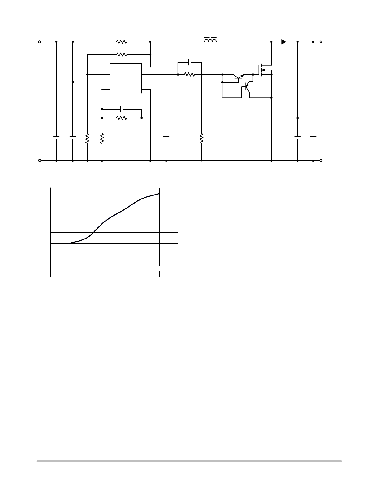
NCP3063, NCP3063B, NCV3063
VIN = 8 B 9 V/0.6 A
C2
C1
330mF 330mF
0V 0V
100nF
R3
M18
R1 0R082
R2 1k
IC1 NCP3063
8
N.C. SWC
7
5
R5 24k
R4
1k
SWE
I
PK
V
CC
COMPTCGND
C3 10n
L1
1
2
36
4
C5 6n8
R7
470R
C4
1n2
R8
1k
10m
NTD18N06
6
2
5
IC2 BC846BPD
1
G
4
3
1N5819
Q1
D
S
D1
100nF
C6
V
OUT
= 31 U/0.35 A
C7
Figure 25. Typical Boost Application Schematic with External NMOS Transistor
86
86
84
84
82
82
80
80
78
78
76
76
EFFICIENCY (%)
74
74
72
72
70
70
6 8 10 12 14 16 18 20
6 8 10 12 14 16 18 20
INPUT VOLTAGE (V)
I
LOAD
= 350 mA
Figure 26. Typical Efficiency for Application
External transistor is recommended in applications where
wide input voltage ranges and higher power is required. The
suitable schematic with an additional NMOS transistor and
its driving circuit is shown in the Figure 25. The driving
circuit is controlled from SWE Pin of the NCP3063 through
frequency compensated resistor divider R7/R8. The driver
IC2 is ON Semiconductor low cost dual NPN/PNP
transistor BC846BPD. Its NPN transistor is connected as a
super diode for charging the gate capacitance. The PNP
transistor works as an emitter follower for discharging the
gate capacitor. This configuration assures sharp driving
edge between 50 - 100 ns as well as it limits power
consumption of R7/R8 divider down to 50 mW. The output
current limit is balanced by resistor R3. The fast switching
with low R
NMOS transistor will achieve efficiencies
DS(on)
up to 85% in automotive applications.
Shown in Figure 25.
+
http://onsemi.com
13

NCP3063, NCP3063B, NCV3063
3
C5
2n2
IC2
Q2
6
2
5
R8
470
C4
6n8
1
4
3
22k
R6
L1
D1
1N5822
100nF
VIN = 8 B 19 V
C1
330mF 330mF
0V 0V
C2
+
100nF
R1 0R050
IC1 NCP3063
8
N.C. SWC
7
5
R2 1k7
R3
1k
SWE
I
PK
V
CC
COMPTCGND
1
2
36
4
R5
1k
NTGS4111P
BC846BPD
C6
10m
V
OUT
C7
Figure 27. Typical Buck Application Schematic with External PMOS Transistor
100
95
90
85
80
75
EFFICIENCY (%)
70
65
60
0 0.5 1 1.5 2 2.5
V
= 8 V
IN
VIN = 18 V
OUTPUT LOAD (Adc)
Figure 28. NCP3063 Efficiency vs. Output Current for
Buck External PMOS at V
T
A
= 3.3 V, f = 220 kHz,
out
= 255C
Figure 27 shows typical buck configuration with external
PMOS transistor. The principle of driving the Q2 gate is the
same as shown in Figure 27.
Resistor R6 connected between TC and SWE pin provides
a pulsed feedback voltage. It is recommended to use this
pulsed feedback approach on applications with a wide input
voltage range, applications with the input voltage over
+12 V or applications with tighter specifications on output
ripple. The suitable value of resistor R6 is between 10k - 2k.
The pulse feedback approach increases the operating
frequency by about 20%. It also creates more regular
switching waveforms with constant operating frequency
which results in lower output ripple voltage and improved
efficiency.
The pulse feedback resistor value has to be selected so that
the capacitor charge and discharge currents as listed in the
electrical characteristic table, are not exceeded. Improper
selection will lead to errors in the oscillator operation. The
maximum voltage at the TC Pin cannot exceed 1.4 V when
implementing pulse feedback.
= 3V3/3 A
+
http://onsemi.com
14

VIN = 8 B 19 V
R1
0R150
NCP3063, NCP3063B, NCV3063
Q1 NSS35200
R4
3
1
2
D2
L1
33m
V
OUT
= 3V3/1 A
33R
IC1 NCP3063
8
N.C. SWC
7
I
PK
V
CC
5
COMPTCGND
R3 1k7
C1
0V 0V
C2
+
100nF
R2
1k
SWE
1
2
36
4
NSR0130
C3
2n2
D1
1N5819
R5
33
C5
100nF
Figure 29. Typical Buck Application Schematic with External Low VCE(sat) PNP Transistor
100
95
90
85
80
75
70
65
EFFICIENCY (%)
60
55
50
0 0.1 0.2 0.3 0.4 0.5 0.6 0.7 0.8 0.9 1
OUTPUT LOAD (Adc)
Typical application of the buck converter with external
bipolar transistor is shown in the Figure 29. It is an ideal
solution for configurations where the input and output
voltage difference is small and high efficiency is required.
NSS35200, the low VCE(
transistor from
sat)
ON Semiconductor will be ideal for applications with 1 A
output current, the input voltages up to 15 V and operating
frequency 100 - 150 kHz. The switching speed could be
improved by using desaturation diode D2.
Figure 30. NCP3063 Efficiency vs. Output Current for
External Low V
at Vin = +5 V, f = 160 kHz,
CE(sat)
= 255C
T
A
C6
+
100mF100mF
http://onsemi.com
15

R1
IC1 NCP3063
8
N.C. SWC
7
I
PK
V
CC
5
COMPTCGND
NCP3063, NCP3063B, NCV3063
1
2
SWE
36
4
R5
22k
L1
R2
C1
R3
0V 0V
C2
10R
R4
4n7
D1C3
C4
Figure 31. Typical Schematic of Buck Converter with RC Snubber and Pulse Feedback
In some cases where there are oscillations on the output
due to the input/output combination, output load variations
or PCB layout a snubber circuit on the SWE Pin will help
minimize the oscillation. Typical usage is shown in the
Figure 31. C3 values can be selected between 2.2 nF and
6.8 nF and R4 can be from 10 W to 22 W.
ORDERING INFORMATION
Device Package Shipping
NCP3063PG PDIP-8
(Pb-Free)
NCP3063BPG PDIP-8
(Pb-Free)
NCP3063BMNTXG DFN-8
(Pb-Free)
NCP3063DR2G SOIC-8
(Pb-Free)
NCP3063BDR2G SOIC-8
(Pb-Free)
NCP3063MNTXG DFN-8
(Pb-Free)
NCV3063PG PDIP-8
(Pb-Free)
NCV3063DR2G SOIC-8
(Pb-Free)
NCV3063MNTXG DFN-8
(Pb-Free)
†For information on tape and reel specifications, including part orientation and tape sizes, please refer to our Tape and Reel Packaging
Specifications Brochure, BRD8011/D.
NCV prefix is for automotive and other applications requiring site and change control.
50 Units / Rail
50 Units / Rail
4000 / Tape & Reel
2500 / Tape & Reel
2500 / Tape & Reel
4000 / Tape & Reel
50 Units / Rail
2500 / Tape & Reel
4000 / Tape & Reel
†
http://onsemi.com
16

-Z-
-Y-
NCP3063, NCP3063B, NCV3063
PACKAGE DIMENSIONS
SOIC-8 NB
CASE 751-07
ISSUE AH
-X-
B
H
A
58
1
4
G
D
0.25 (0.010) Z
M
S
Y
0.25 (0.010)
C
SEATING
PLANE
SXS
M
0.10 (0.004)
M
Y
K
N
X 45
_
M
J
NOTES:
1. DIMENSIONING AND TOLERANCING PER
ANSI Y14.5M, 1982.
2. CONTROLLING DIMENSION: MILLIMETER.
3. DIMENSION A AND B DO NOT INCLUDE
MOLD PROTRUSION.
4. MAXIMUM MOLD PROTRUSION 0.15 (0.006)
PER SIDE.
5. DIMENSION D DOES NOT INCLUDE DAMBAR
PROTRUSION. ALLOWABLE DAMBAR
PROTRUSION SHALL BE 0.127 (0.005) TOTAL
IN EXCESS OF THE D DIMENSION AT
MAXIMUM MATERIAL CONDITION.
6. 751-01 THRU 751-06 ARE OBSOLETE. NEW
STANDARD IS 751-07.
MILLIMETERS
DIMAMIN MAX MIN MAX
4.80 5.00 0.189 0.197
B 3.80 4.00 0.150 0.157
C 1.35 1.75 0.053 0.069
D 0.33 0.51 0.013 0.020
G 1.27 BSC 0.050 BSC
H 0.10 0.25 0.004 0.010
J 0.19 0.25 0.007 0.010
K 0.40 1.27 0.016 0.050
M 0 8 0 8
____
N 0.25 0.50 0.010 0.020
S 5.80 6.20 0.228 0.244
INCHES
SOLDERING FOOTPRINT*
1.52
0.060
7.0
0.275
0.6
0.024
*For additional information on our Pb-Free strategy and soldering
details, please download the ON Semiconductor Soldering and
Mounting Techniques Reference Manual, SOLDERRM/D.
4.0
0.155
1.270
0.050
SCALE 6:1
ǒ
inches
mm
Ǔ
http://onsemi.com
17

NOTE 2
-T-
SEATING
PLANE
H
58
-B-
14
F
-A-
C
N
D
G
0.13 (0.005) B
NCP3063, NCP3063B, NCV3063
PACKAGE DIMENSIONS
8 LEAD PDIP
CASE 626-05
ISSUE L
L
J
K
M
M
A
T
M
M
NOTES:
1. DIMENSION L TO CENTER OF LEAD WHEN
FORMED PARALLEL.
2. PACKAGE CONTOUR OPTIONAL (ROUND OR
SQUARE CORNERS).
3. DIMENSIONING AND TOLERANCING PER ANSI
Y14.5M, 1982.
DIM MIN MAX MIN MAX
A 9.40 10.16 0.370 0.400
B 6.10 6.60 0.240 0.260
C 3.94 4.45 0.155 0.175
D 0.38 0.51 0.015 0.020
F 1.02 1.78 0.040 0.070
G 2.54 BSC 0.100 BSC
H 0.76 1.27 0.030 0.050
J 0.20 0.30 0.008 0.012
K 2.92 3.43 0.115 0.135
L 7.62 BSC 0.300 BSC
M --- 10 --- 10
N 0.76 1.01 0.030 0.040
STYLE 1:
PIN 1. AC IN
2. DC + IN
3. DC - IN
4. AC IN
5. GROUND
6. OUTPUT
7. AUXILIARY
8. V
CC
INCHESMILLIMETERS
__
http://onsemi.com
18
IDENTIFICATION
l
2X
8X
SEATING
PLANE
2X
PIN ONE
C0.10
C0.08
C0.15
A1
TOP VIEW
C0.15
SIDE VIEW
NCP3063, NCP3063B, NCV3063
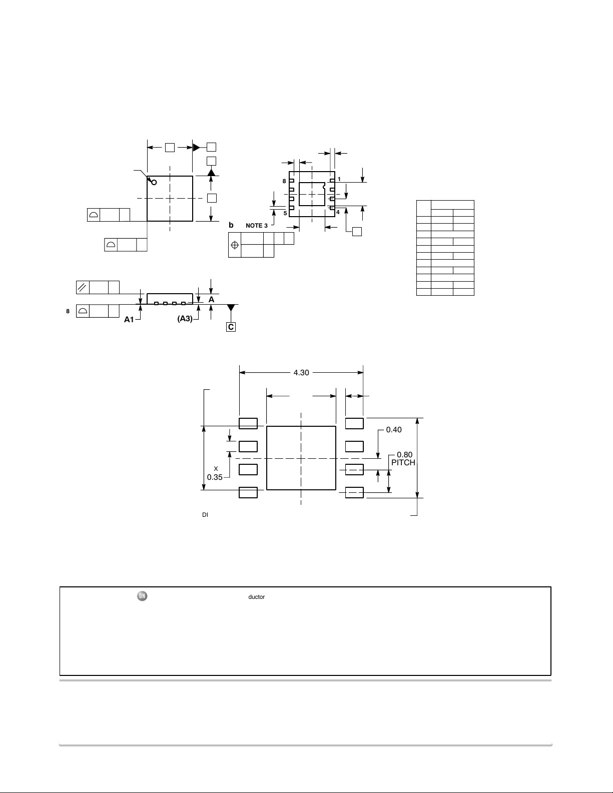
PACKAGE DIMENSIONS
8 PIN DFN, 4x4
CASE 488AF-01
ISSUE B
NOTES:
D
A
B
E
b NOTE 3
8X
0.10 C
0.05 C
K
8X
8
5
AB
BOTTOM VIEW
8X L
E2
1
D2
4
e
A
(A3)
C
1. DIMENSIONS AND TOLERANCING PER
ASME Y14.5M, 1994.
2. CONTROLLING DIMENSION: MILLIMETERS.
3. DIMENSION b APPLIES TO PLATED
TERMINAL AND IS MEASURED BETWEEN
0.25 AND 0.30 MM FROM TERMINAL.
4. COPLANARITY APPLIES TO THE EXPOSED
PAD AS WELL AS THE TERMINALS.
MILLIMETERS
DIM MIN MAX
A 0.80 1.00
A1 0.00 0.05
A3 0.20 REF
b 0.25 0.35
D 4.00 BSC
D2 1.91 2.21
E 4.00 BSC
E2 2.09 2.39
e 0.80 BSC
K 0.20 ---
L 0.30 0.50
SOLDERING FOOTPRINT*
4.30
2.21
1
8X
2.39
0.35
DIMENSIONS: MILLIMETERS
*For additional information on our Pb-Free strategy and soldering
details, please download the ON Semiconductor Soldering and
Mounting Techniques Reference Manual, SOLDERRM/D.
ON Semiconductor and are registered trademarks of Semiconductor Components Industries, LLC (SCILLC). SCILLC reserves the right to make changes without further notice
to any products herein. SCILLC makes no warranty, representation or guarantee regarding the suitability of its products for any particular purpose, nor does SCILLC assume any liability
arising out of the application or use of any product or circuit, and specifically disclaims any and all liability, including without limitation special, consequential or incidental damages.
“Typical” parameters which may be provided in SCILLC data sheets and/or specifications can and do vary in different applications and actual performance may vary over time. All
operating parameters, including “Typicals” must be validated for each customer application by customer's technical experts. SCILLC does not convey any license under its patent rights
nor the rights of others. SCILLC products are not designed, intended, or authorized for use as components in systems intended for surgical implant into the body, or other applications
intended to support or sustain life, or for any other application in which the failure of the SCILLC product could create a situation where personal injury or death may occur. Should
Buyer purchase or use SCILLC products for any such unintended or unauthorized application, Buyer shall indemnify and hold SCILLC and its officers, employees, subsidiaries, affiliates,
and distributors harmless against all claims, costs, damages, and expenses, and reasonable attorney fees arising out of, directly or indirectly, any claim of personal injury or death
associated with such unintended or unauthorized use, even if such claim alleges that SCILLC was negligent regarding the design or manufacture of the part. SCILLC is an Equal
Opportunity/Affirmative Action Employer. This literature is subject to all applicable copyright laws and is not for resale in any manner.
8X
0.63
0.40
PITCH
2.75
0.80
PUBLICATION ORDERING INFORMATION
LITERATURE FULFILLMENT:
Literature Distribution Center for ON Semiconductor
P.O. Box 5163, Denver, Colorado 80217 USA
Phone: 303-675-2175 or 800-344-3860 Toll Free USA/Canada
Fax: 303-675-2176 or 800-344-3867 Toll Free USA/Canada
Email: orderlit@onsemi.com
N. American Technical Support: 800-282-9855 Toll Free
USA/Canada
Europe, Middle East and Africa Technical Support:
Phone: 421 33 790 2910
Japan Customer Focus Center
Phone: 81-3-5773-3850
http://onsemi.com
19
ON Semiconductor Website: www.onsemi.com
Order Literature: http://www.onsemi.com/orderlit
For additional information, please contact your loca
Sales Representative
NCP3063/D
 Loading...