

ON Semiconductor NCP1608BOOSTGEVB User Manual
NCP1608BOOSTGEVB
NCP1608 100 W Boost
Evaluation Board User's
Manual
http://onsemi.com
Introduction
The NCP1608 is a voltage mode power factor correction
(PFC) controller designed to implement converters to
comply with line current harmonic regulations. The device
operates in critical conduction mode (CrM) for optimal
performance in applications up to 350 W. Its voltage mode
scheme enables it to obtain near unity power factor (PF)
without the need for a line-sensing network. The output
voltage is accurately controlled with an integrated high
precision transconductance error amplifier. The controller
also implements a comprehensive set of safety features that
simplify system design.
This application note describes the design and
implementation of a 400 V, 100 W, CrM boost PFC
converter using the NCP1608. The converter exhibits high
PF, low standby power dissipation, high active mode
efficiency, and a variety of protection features.
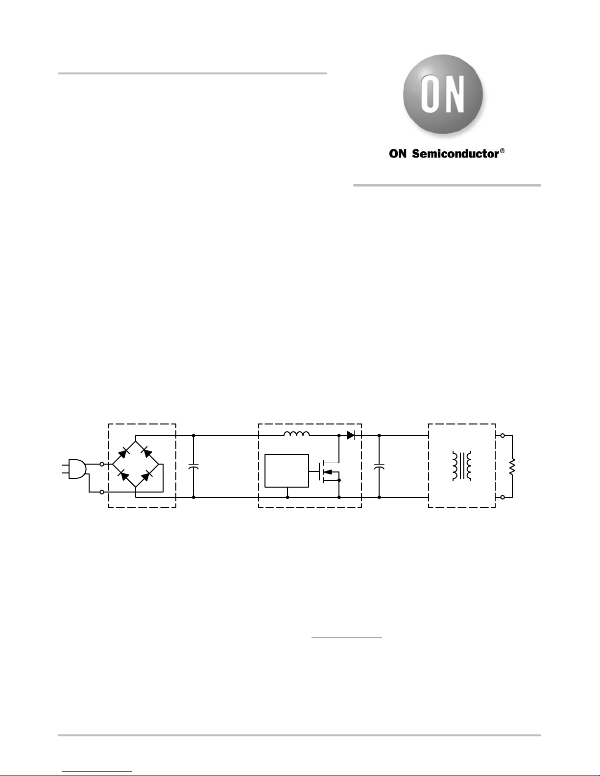
PFC Pre−Converter
NCP1608
AC Line
Rectifiers
+
High
Frequency
Bypass
Capacitor
EVAL BOARD USER’S MANUAL
The Need for PFC
Most electronic ballasts and switch−mode power supplies
(SMPS) use a diode bridge rectifier and a bulk storage
capacitor to produce a dc voltage from the utility ac line.
This causes a non-sinusoidal current consumption and
increases the stress on the power delivery infrastructure.
Government regulations and utility requirements mandate
control over line current harmonic content. Active PFC
circuits are the most popular method to comply with these
harmonic content requirements. System solutions consist of
connecting a PFC pre−converter between the rectifier bridge
and the bulk capacitor (Figure 1). The boost converter is the
most popular topology for active PF correction. It produces
a constant output voltage and consumes a sinusoidal input
current from the line.
Converter
Bulk
+
Storage
Capacitor
Load
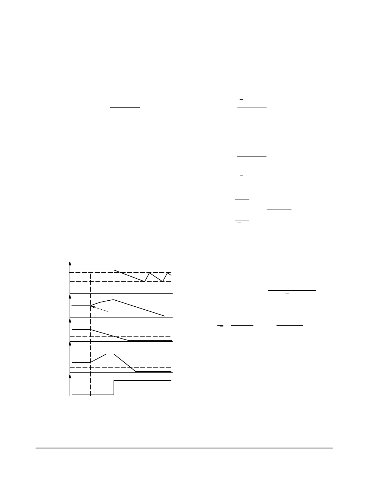
Basic Operation of a CrM Boost Converter
For medium power (< 350 W) applications, CrM is the
preferred control method. CrM operates at the boundary
between discontinuous conduction mode (DCM) and
continuous conduction mode (CCM). In CrM, the drive on
time begins when the inductor current reaches zero.
CrM combines the reduced peak current of CCM
operation with the zero current switching of DCM
© Semiconductor Components Industries, LLC, 2012
November, 2012 − Rev. 1
Figure 1. Active PFC Stage with the NCP1608
operation. This control method causes the frequency to vary
with the instantaneous line input voltage (V
load. The operation and waveforms of a CrM PFC boost
converter are illustrated in Figure 2. For detailed
information on the operation of a CrM boost converter for
PFC applications, please refer to AND8123 at
www.onsemi.com
1 Publication Order Number:
.
) and the output
in
EVBUM2162/D
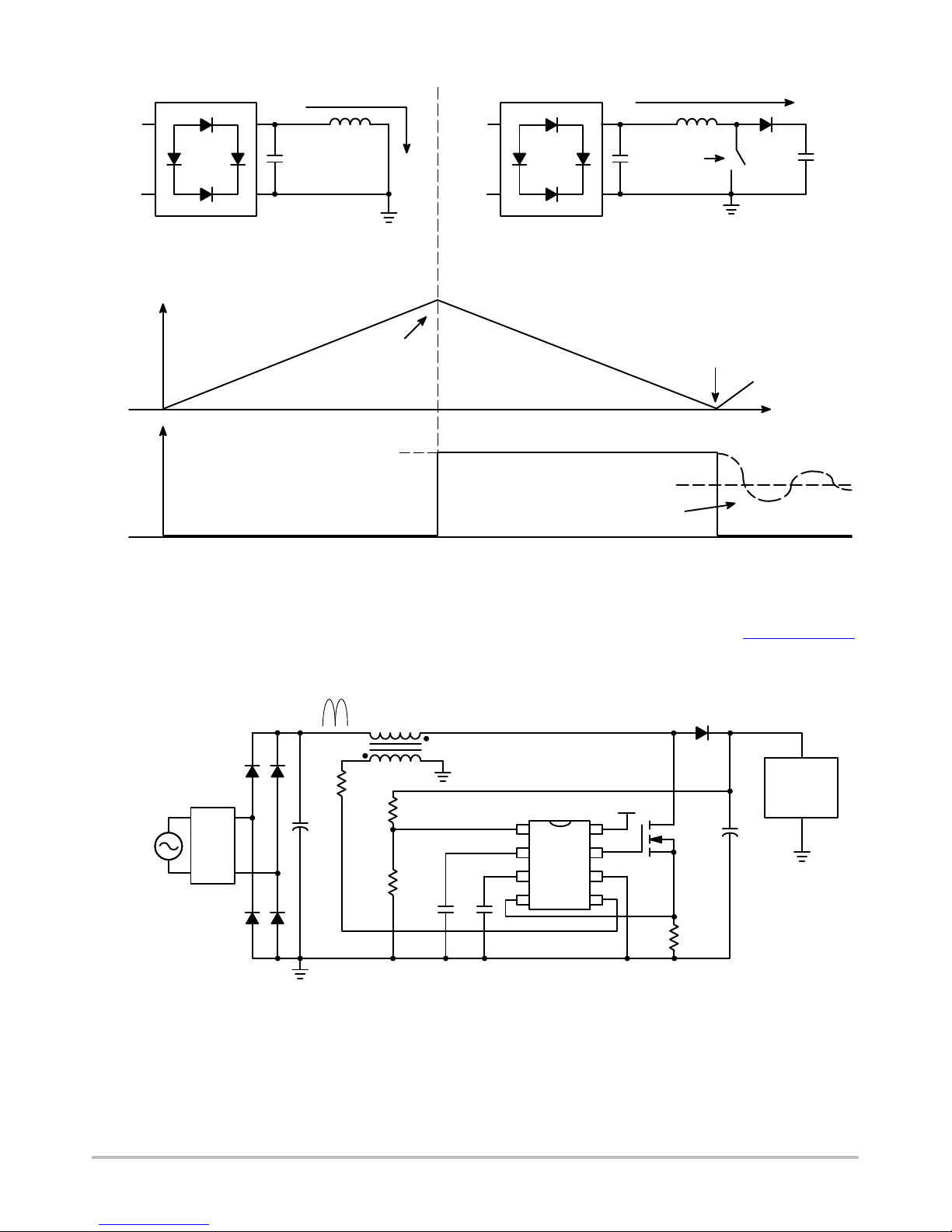
NCP1608BOOSTGEVB
Diode Bridge
V
in
AC Line
+
+
L
−
The power switch is ON The power switch is OFF
With the power switch voltage being about zero, the
input voltage is applied across the inductor. The inductor current linearly increases with a (Vin/L) slope.
Inductor
Current
Vin/L
I
V
drain
V
out
I
L
V
drain
L(peak)
Diode Bridge
V
in
+
V
drain
L
+
AC Line
−
The inductor current flows through the diode. The inductor
voltage is (V
with a (V
− Vin) and the inductor current linearly decays
out
− Vin)/L slope.
out
(V
− Vin)/L
out
Critical Conduction Mode:
Next current cycle starts
when the core is reset.
V
in
If next cycle does not start
then V
rings towards V
drain
in
I
L
+
V
out
Figure 2. Schematic and Waveforms of an Ideal CrM Boost Converter
Features of the NCP1608
The NCP1608 is an excellent controller for robust
medium power CrM boost PFC applications due to its
integrated safety features, low impedance driver, high
precision error amplifier, and low standby current
consumption.
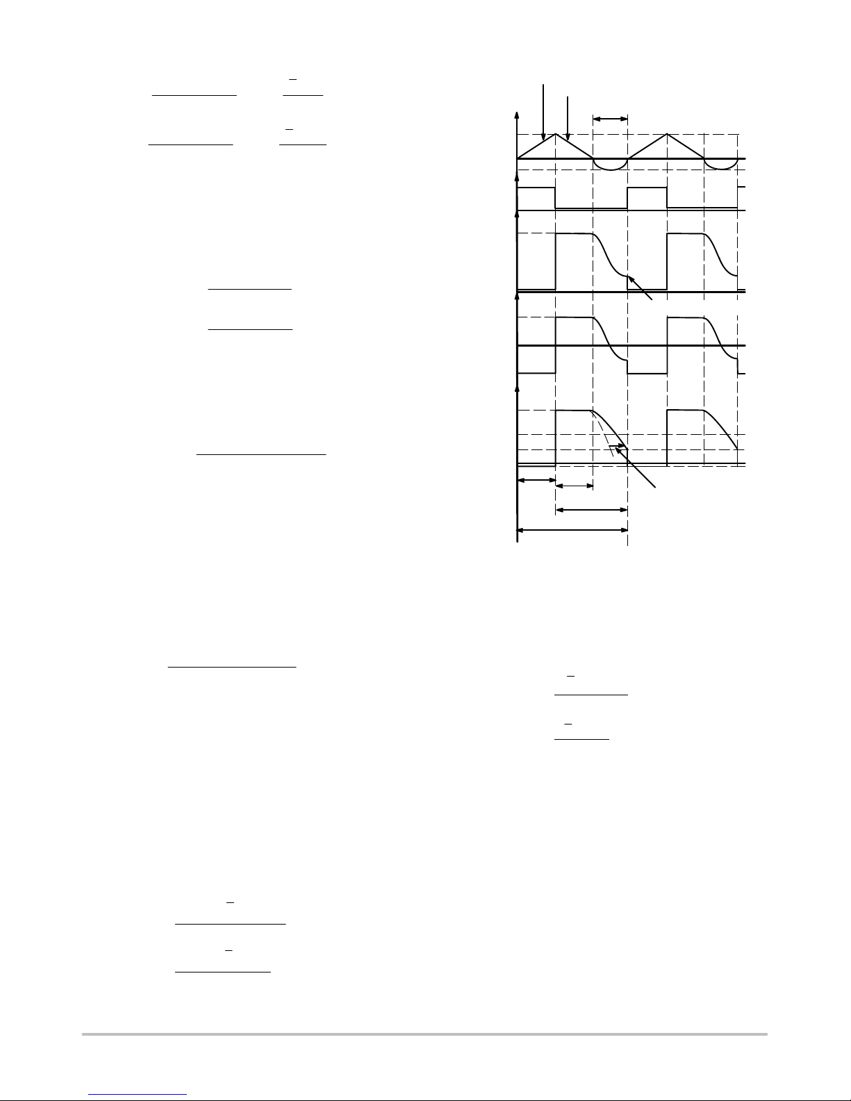
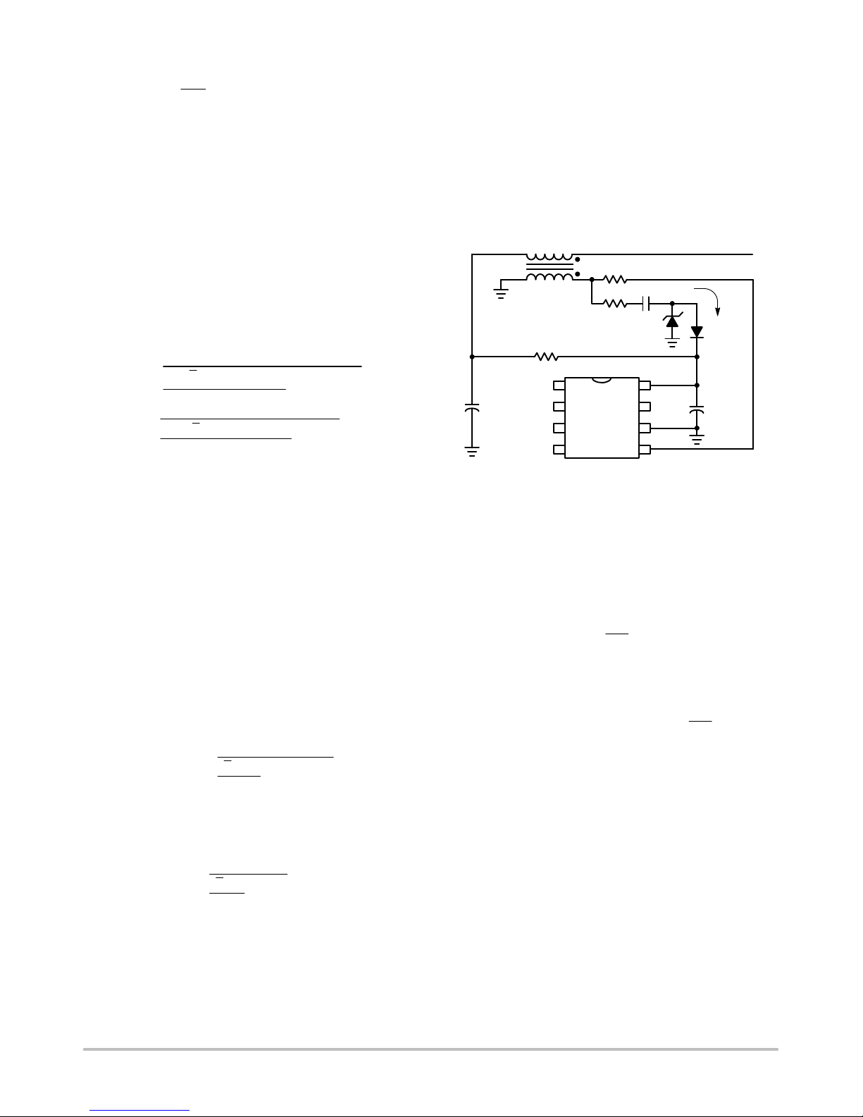
AC Line
EMI
Filter
V
in
R
ZCD
+
C
in
Figure 3. CrM Boost PFC Stage Featuring the NCP1608
L
R
out1
R
out2
C
COMP
For detailed information on the operation of the
NCP1608, please refer to NCP1608/D at www.onsemi.com
A CrM boost pre-converter featuring the NCP1608 is
shown in Figure 3.
M
R
D
sense
+
C
bulk
NB:N
C
t
ZCD
1
2
3
4
NCP1608
V
FB
Control
DRV
CtCSGND
ZCD
V
CC
8
CC
7
6
5
V
out
LOAD
(Ballast,
SMPS, etc.)
.
The FB pin senses the boost output voltage through the
resistor divider formed by R
out1
and R
includes overvoltage protection (OVP), undervoltage
protection (UVP), and floating pin protection (FPP). This
pin is the input to the error amplifier. The output of the error
amplifier is the Control pin.
. The FB pin
out2
A combination of resistors and capacitors connected
between the Control and ground pins forms a compensation
network that limits the bandwidth of the converter. For high
PF, the bandwidth is set to less than 20 Hz. A capacitor
connected to the Ct pin sets the maximum on time. The CS
pin provides cycle−by−cycle overcurrent protection. The
http://onsemi.com
2

NCP1608BOOSTGEVB
internal comparator compares the voltage developed across
R
(VCS) to an internal reference (V
sense
turns off when V
reaches V
CS
. The ZCD pin senses the
ILIM
). The driver
ILIM
demagnetization of the boost inductor to turn on the drive.
The drive on time begins after the ZCD pin voltage (V
exceeds V
V
ZCD(TRIG)
ZCD(ARM)
. A resistor in series with the ZCD winding
and then decreases to less than
ZCD
)
limits the ZCD pin current.
The NCP1608 features a powerful output driver on the
DRV pin. The driver is capable of switching the gates of
large MOSFETs efficiently because of its low source and
sink impedances. The driver includes active and passive
pull−down circuits to prevent the output from floating high
when the NCP1608 is disabled.
Table 1. Additional Resources for the Design and Understanding of CrM Boost PFC Circuits Available at
www.onsemi.com
AND8123 Power Factor Correction Stages Operating in Critical Conduction Mode
AND8016 Design of Power Factor Correction Circuits Using the MC33260
AND8154 NCP1230 90 W, Universal Input Adapter Power Supply with Active PFC
HBD853 Power Factor Correction Handbook
DESIGN STEP 1: Define the Required Parameters
.
The V
is less than the turn on voltage (V
pin is the supply pin of the controller. When V
CC
CC(on)
consumption of the device is less than 35 mA. This results in
fast startup times and reduced standby power losses.
Design Procedure
The design of a CrM boost PFC converter is discussed in
many ON Semiconductor application notes. Table 1 lists
some examples.
This application note describes the design procedure for
a 400 V, 100 W converter using the features of the NCP1608.
A dedicated NCP1608 design tool that enables users to
determine component values quickly is available at
www.onsemi.com
.
The converter parameters are shown in Table 2.
CC
), the current
Table 2. CONVERTER PARAMETERS
Parameter Name Symbol Value Units
Minimum Line Input Voltage Vac
Maximum Line Input Voltage Vac
Minimum Line Frequency f
Maximum Line Frequency f
Output Voltage V
Full Load Output Current I
Full Load Output Power P
Maximum Output Voltage V
Minimum Switching Frequency f
Minimum Full Load Efficiency
Minimum Full Load Power Factor PF 0.9 −
DESIGN STEP 2: Calculate the Boost Inductor
The value of the boost inductor (L) is calculated using
Equation 1:
V
out
2
ǒ
Vac
L v
@
Ǹ
@ V
2
out
* VacǓ@ h
Ǹ
2
@ P
out
@ f
SW(MIN)
(eq. 1)
To ensure that the switching frequency exceeds the
minimum frequency, L is calculated at both the minimum
and maximum rms input line voltage:
400
2
ǒ
85
LLLv
@
Ǹ
2
* 85Ǔ@ 0.92
Ǹ
2
@ 400 @ 100 @ 40 k
+ 581 mH
LL
HL
line(MIN)
line(MAX)
out
out
out
out(MAX)
SW(MIN)
h
Where LLLis the inductor value calculated at VacLL.
v
L
HL
Where L
85 Vac
265 Vac
47 Hz
63 Hz
400 V
250 mA
100 W
440 V
40 kHz
92 %
400
2
ǒ
265
@
Ǹ
2
is the inductor value calculated at VacHL.
HL
* 265Ǔ@ 0.92
Ǹ
2
@ 400 @ 100 @ 40 k
+ 509 mH
A value of 400 mH is selected. The inductance tolerance
is ±15%. The maximum inductance (L
MAX
) value is
460 mH. Equation 2 is used to calculate the minimum
frequency at full load.
fSW+
2 @ L
Vac
MAX
2
@ h
@ǒ1 *
@ P
out
Ǹ
@ Vac
2
V
out
Ǔ
(eq. 2)
http://onsemi.com
3
NCP1608BOOSTGEVB
f
SW(LL)
f
SW(HL)
2
@ 0.92
85
+
2 @ 460 m @ 100
2
@ 0.92
265
+
2 @ 460 m @ 100
@ǒ1 *
@ǒ1 *
Ǹ
Ǹ
2
400
@ 265
2
400
@ 85
Ǔ
+ 50.5 kHz
Ǔ
+ 44.3 kHz
fSW is equal to 50.5 kHz at VacLL and 44.3 kHz at VacHL.
DESIGN STEP 3: Size the Ct Capacitor
The Ct capacitor is sized to set the maximum on time for
minimum line input voltage and maximum output power.
The maximum on time is calculated using Equation 3:
t
on(MAX)
t
on(MAX)
2 @ L
+
2 @ 460 m @ 100
+
MAX
h @ Vac
0.92 @ 85
@ P
LL
out
2
+ 13.8 ms
2
(eq. 3)
Sizing Ct to an excessively large value causes the
application to deliver excessive output power and reduces
the control range at Vac
or low output power. It is
HL
recommended to size the Ct capacitor to a value slightly
larger than that calculated by Equation 4:
Where I
charge
Ct w
and V
2 @ P
Ct(MAX)
@ L
out
h @ Vac
@ I
MAX
charge
2
@ V
LL
Ct(MAX)
are specified in the NCP1608
(eq. 4)
datasheet. To ensure that the controller sets the maximum on
time to a value sufficient to deliver the required output
power, the maximum I
and the minimum V
charge
Ct(MAX)
values are used in the calculations for Ct.
From the NCP1608 datasheet:
− V
− I
Ct(MAX)
charge
= 4.775 V (minimum)
= 297 mA (maximum)
Ct is equal to:
2 @ 100 @ 460 m @ 297 m
Ct w
0.92 @ 85
2
@ 4.775
+ 860 pF
A normalized value of 1 nF (±10%) provides sufficient
margin. A value of 1.22 nF is selected for Total Harmonic
Distortion (THD) reduction (see the Additional THD
Reduction section of this application note for more
information).
DESIGN STEP 4: Determine the ZCD Turns Ratio
To activate the ZCD detector of the NCP1608, the ZCD
turns ratio is sized such that at least V
ZCD(ARM)
(1.55 V
maximum) is applied to the ZCD pin during all operating
conditions (see Figure 4). The boost winding to ZCD
winding turns ratio (N = N
B:NZCD
) is calculated using
Equation 5.
N v
N v
V
*ǒ2Ǹ@ Vac
out
V
400 *
ZCD(ARM)
ǒ
2Ǹ@ 265
1.55
HL
Ǔ
+ 16
Ǔ
(eq. 5)
I
L(peak)
I
L(NEG)
DRV
V
V
ZCD(WIND)
V
ZCD(WIND),off
V
ZCD(WIND),on
V
V
CL(POS)
V
ZCD(ARM)
V
ZCD(TRIG)
V
CL(NEG)
MOSFET Conduction
I
L
drain
V
out
ZCD
Diode Conduction
t
diode
t
on
t
T
SW
t
z
0 A
0 V
0 V
Minimum Voltage Turn on
0 V
0 V
R
off
ZCD
Delay
Figure 4. Realistic CrM Waveforms Using a ZCD
Winding with R
A turns ratio of 10 is selected for this design. R
and the ZCD Pin Capacitance
ZCD
ZCD
is
connected between the ZCD winding and the ZCD pin to
limit the ZCD pin current. This current must be limited
below 10 mA. R
R
R
The value of R
is calculated using Equation 6:
ZCD
ZCD
ZCD
2Ǹ@ Vac
w
I
ZCD(MAX)
Ǹ
2
w
10 m @ 10
and the parasitic capacitance of the
ZCD
@ 265
HL
@ N
+ 3.75 kW
(eq. 6)
ZCD pin determine when the ZCD winding signal is
detected and the drive turn on begins. A large R
ZCD
value
creates a long delay before detecting the ZCD event. In this
case, the controller operates in DCM and the PF is reduced.
If the R
value is too small, the drive turns on when the
ZCD
drain voltage is high and efficiency is reduced. A popular
strategy for selecting R
is to use the R
ZCD
value that
ZCD
achieves minimum drain voltage turn on. This value is found
experimentally.
During the delay caused by R
capacitance, the equivalent drain capacitance (C
and the ZCD pin
ZCD
EQ(drain)
discharges through the path shown in Figure 5.
)
http://onsemi.com
4
NCP1608BOOSTGEVB
L
I
L
I
AC Line
in
EMI
Filter
+
C
in
Figure 5. Equivalent Drain Capacitance Discharge Path
C
EQ(drain)
MOSFET, the diode, and the inductor. C
energy discharged by C
biases the bridge rectifier and causes the input current (I
is the combined parasitic capacitances of the
is charged by the
in
EQ(drain)
. The charging of Cin reverse
in
to decrease to zero. The zero input current causes THD to
increase. To reduce THD, the ratio (t
where t
turns on. The ratio (t
is the period from when IL = 0 A to when the drive
Z
/ TSW) is inversely proportional to the
z
/ TSW) is minimized,
z
square root of L.
DESIGN STEP 5: Set the FB, OVP, and UVP Levels
R
and R
out1
V
before it is applied to the FB pin. The error amplifier
out
form a resistor divider that scales down
out2
adjusts the on time of the drive to maintain the FB pin
voltage equal to the error amplifier reference voltage
(V
). The divider network bias current (I
REF
bias(out)
selection is the first step in the calculation. The divider
network bias current is selected to optimize the tradeoff of
noise immunity and power dissipation. R
is calculated
out1
using the optimized bias current and output voltage using
Equation 7:
V
+
out
I
bias(out)
R
out1
(eq. 7)
A bias current of 100 mA provides an acceptable tradeoff
of power dissipation to noise immunity.
+
400
100 m
+ 4MW
R
out1
The output voltage signal is delayed before it is applied to
the FB pin due to the time constant set by R
pin capacitance. R
must not be sized too large or this
out1
and the FB
out1
delay may cause overshoots of the OVP detection voltage.
R
is dependent on V
out2
feedback resistor (R
table). R
is calculated using Equation 8:
out2
, shown in the NCP1608 specification
FB
out
, R
, and the internal
out1
V
@ R
out
+
C
bulk
FB
out1
+ 25.3 kW
D
C
EQ(drain)
R
R
+
out2
RFB@
)
R
+
out2
4.6 M @
R
is selected as 25.5 kW for this design.
out2
out1
V
out
ǒ
* 1Ǔ* R
V
REF
4M@ 4.6 M
400
ǒ
* 1Ǔ* 4M
2.5
Using the selected resistor, the resulting output voltage is
calculated using Equation 9:
R
) R
V
+ V
out
V
+ 2.5 @ǒ4M@
)
out
REF
@ǒR
out2
@
out1
R
out2
25.5 k ) 4.6 M
25.5 k @ 4.6 M
FB
) 1
@ R
FB
) 1Ǔ+ 397 V
The low bandwidth of the PFC stage causes overshoots
during transient loads or during startup. The NCP1608
includes an integrated OVP circuit to prevent the output
from exceeding a safe voltage. The OVP circuit compares
V
to the internal overvoltage detect threshold voltage to
FB
determine if an OVP fault occurs. The OVP detection
voltage is calculated using Equation 10:
V
V
out(OVP)
V
out(OVP)
OVP
+
+ 1.06 @ 2.5 @ǒ4M@
@ V
V
REF
The output capacitor (C
REF
@ǒR
bulk
R
) R
out2
@
out1
R
@ R
out2
25.5 k ) 4.6 M
25.5 k @ 4.6 M
) 1Ǔ+ 421 V
) value is sized to be large
enough so that the peak-to-peak output voltage ripple
(V
ripple(peak-peak)
C
is calculated using Equation 11:
bulk
C
bulk
Where f
and V
line
ripple(peak-peak)
) is less than the OVP detection voltage.
P
w
2 @ p @ V
ripple(peak−peak)
out
@ f
line
@ V
= 47 Hz is the worst case for the ripple voltage
< 42 V.
C
w
bulk
2 @ p @ 42 @ 47 @ 400
100
+ 20 mF
(eq. 8)
Ǔ
(eq. 9)
(eq. 10)
FB
Ǔ
) 1
FB
(eq. 11)
out
http://onsemi.com
5
NCP1608BOOSTGEVB
Ǹ
The value of C
V
ripple(peak-peak)
is selected as 68 mF to reduce
bulk
to less than 15 V. This results in a peak
output voltage of 406.25 V, which is less than the peak output
OVP detection voltage (421 V).
The NCP1608 includes undervoltage protection (UVP).
During startup, C
voltage. If C
bulk
charges to the peak of the ac line
bulk
does not charge to a minimum voltage, the
NCP1608 detects an UVP fault. The UVP detection voltage
is calculated using Equation 12:
V
out(UVP)
V
out(UVP)
+ V
+ 0.31 @ǒ4M@
UVP
@ǒR
out1
out2
@
R
out2
25.5 k ) 4.6 M
25.5 k @ 4.6 M
@ R
FB
FB
Ǔ
) 1
(eq. 12)
) 1Ǔ+ 49 V
R
) R
The UVP feature protects against open loop conditions in
the feedback loop. If the FB pin is inadvertently floating
(perhaps due to a bad solder joint), the coupling within the
system may cause V
V
< VFB < V
UVP
to be within the regulation range (i.e.
FB
). The controller responds by delivering
REF
maximum power. The output voltage increases and over
stresses the components. The NCP1608 includes a feature to
protect the system if FB is floating. The internal pull-down
resistor (R
) ensures that VFB is below the UVP threshold
FB
if the FB pin is floating.
If the FB pin floats during operation, V
decreasing from V
. The rate of decrease depends on R
REF
begins
FB
FB
and the FB pin parasitic capacitance. As VFB decreases,
V
V
increases, which causes the on time to increase until
Control
FB
< V
. When VFB < V
UVP
, the UVP fault is detected
UVP
and the controller is disabled. The sequence is depicted in
Figure 6.
V
CC
V
CC(on)
V
CC(off)
V
out
V
out
Loop is Opened
V
FB
V
REF
V
UVP
V
Control
V
EAH
Ct
(offset)
UVP Fault
Figure 6. UVP Operation if Loop is Opened During
Operation
DESIGN STEP 6: Size the Power Components
The power components are sized such that there is
sufficient margin to sustain the currents and voltages applied
to them. At minimum line input voltage and maximum
output power the inductor peak current is at the maximum,
which causes the greatest stress to the power components.
The components are referenced in Figure 3.
1. The inductor peak current (I
L(peak)
) is calculated
using Equation 13:
+
Ǹ
+
2Ǹ@ 2 @ P
2
0.92 @ 85
I
L(peak)
I
L(peak)
The inductor rms current (I
h @ Vac
@ 2 @ 100
out
+ 3.62 A
L(RMS)
(eq. 13)
) is calculated using
Equation 14:
2 @ P
I
+
L(RMS)
I
+
L(RMS)
Ǹ
2. The output diode (D) rms current (I
out
3Ǹ@ Vac @ h
2 @ 100
@ 85 @ 0.92
3
+ 1.48 A
D(RMS)
(eq. 14)
) is
calculated using Equation 15:
I
D(RMS)
I
D(RMS)
+
+
Ǹ
@
3
4
3
p
Ǹ
@ 2
2
Ǹ
@
p
Ǹ
@ 2
2
4
The diode maximum voltage is equal to V
P
@
@
out
Ǹ
h @ Vac @ V
100
Ǹ
0.92 @ 85 @ 400
out
+ 0.75 A
(421 V)
OVP
(eq. 15)
plus the overshoot caused by parasitic contributions. For this
evaluation board, the maximum voltage is 450 V. A 600 V
diode provides a 25% derating factor. The MUR460
(4 A/600 V) diode is selected for this design.
3. The MOSFET (M) rms current (I
M(RMS)
) is
calculated using Equation 16:
P
I
M(RMS)
I
M(RMS)
+
+
2
Ǹ
3
2
Ǹ
3
ǒ
@
h @ Vac
ǒ
@
0.92 @ 85
out
100
Ǔ
@ 1 *
Ǹ
Ǔ
@ 1−
The MOSFET maximum voltage is equal to V
2Ǹ@ 8 @ Vac
ǒ
3 @ p @ V
2Ǹ@ 8 @ 85
ǒ
3 @ p @ 400
Ǔ
out
Ǔ
+1.27 A
(eq. 16)
OVP
(421 V) plus the overshoot caused by parasitic
contributions. For this evaluation board, the maximum
voltage is 450 V. A 560 V MOSFET provides a 20% derating
factor. The SPP12N50C3 (11.6 A/560 V) MOSFET is
selected for this design.
4. The current sense resistor (R
) limits the
sense
maximum inductor peak current of the MOSFET
and is calculated using Equation 17:
V
+
ILIM
I
L(peak)
(eq. 17)
R
sense
Where V
http://onsemi.com
6
is specified in the NCP1608 datasheet.
ILIM
NCP1608BOOSTGEVB
+
0.5
3.62
+ 0.138 W
R
sense
The current sense resistor is selected as 0.125 W for
decreased power dissipation. The resulting maximum
inductor peak current is 4 A. Since the MOSFET continuous
current rating is 7 A (for T
= 100°C as specified in the
C
manufacturer’s datasheet) and the inductor saturation
current is 4.7 A, the maximum peak inductor current of 4 A
is sufficiently low.
The power dissipated by R
is calculated using
sense
Equation 18:
P
P
+ I
R
sense
+ 1.272@ 0.125 + 0.202 W
R
sense
5. The output capacitor (C
M(RMS)
2
@ R
sense
) rms current is
bulk
(eq. 18)
calculated using Equation 19:
I
+
C(RMS)
I
+
C(RMS)
The value of C
Ǹ
Ǹ
2Ǹ@ 32 @ P
9 @ p @ Vac @ V
Ǹ
@ 32 @ 100
2
9 @ p @ 85 @ 400 @ 0.92
is calculated in Step 5 to ensure a ripple
bulk
out
out
2
@ h
2
* I
2
* 0.25
2
load(RMS)
2
+ 0.7 A
2
(eq. 19)
voltage that is sufficiently low to not trigger OVP. The value
of C
does not exceed the ratings of C
V
may need to be increased so that the rms current
bulk
.
bulk
The voltage rating of C
out(OVP)
. Since V
out(OVP)
is required to be greater than
bulk
is 421 V, C
is selected to have
bulk
a voltage rating of 450 V.
DESIGN STEP 7: Supply VCC Voltage
The typical method to charge the VCC capacitor (C
V
is to connect a resistor between Vin and VCC. The
CC(on)
Vcc
) to
low startup current consumption of the NCP1608 enables
most of the resistor current to charge C
during startup.
Vcc
The low startup current consumption enables faster startup
times and reduces standby power dissipation. The startup
time (t
Where I
If C
selected as 660 kW, t
) is approximated with Equation 20:
startup
C
@ V
V
CC(on)
t
+
startup
CC(startup)
is selected as a 47 mF capacitor and R
Vcc
= 24 mA (typical).
startup
t
+
startup
2Ǹ@Vac
R
start
is equal to:
47 m @ 12
Ǹ
@85
2
660 k
CC
* I
* 24 m
CC(startup)
+ 3.57 s
(eq. 20)
start
is
Once VCC reaches V
, the internal references and
CC(on)
logic of the NCP1608 turn on. The NCP1608 includes an
undervoltage lockout (UVLO) feature that ensures that the
NCP1068 remains enabled unless V
V
supply to power V
. This hysteresis ensures sufficient time for another
CC(off)
.
CC
decreases to less than
CC
The ZCD winding is a possible solution, but the voltage
induced on the winding may be less than the required
voltage. An alternative is to implement a charge pump to
supply V
Figure 7. The ZCD Winding Supplies V
. A schematic is illustrated in Figure 7.
CC
R
ZCD
C
R
1
D
AUX
R
start
NCP1608
1
+
C
in
2
3
4
FB
Control
Ct
CS
V
CC
DRV
GND
ZCD
8
7
6
5
Charge Pump Circuit
I
3
AUX
D
1
+
C
Vcc
using a
CC
C3 stores the energy for the charge pump. R1 limits the
current by reducing the rate of voltage change. D
AUX
supplies
current to C3 when its cathode is negative. When its cathode
is positive it limits the maximum voltage applied to V
CC
.
The voltage change across C3 over one period is
calculated using Equation 21:
V
DVC3+
The current that charges C
N
out
* V
CC
is calculated using
Vcc
(eq. 21)
Equation 22:
(eq. 22)
V
out
I
+ C3 @ fSW@ DVC3+ C3 @ fSW@
AUX
ǒ
N
* V
CC
Ǔ
For off−line ac-dc applications that require PFC, a 2-stage
approach is typically used. The first stage is the CrM boost
PFC. This supplies the 2nd stage, which is traditionally an
isolated flyback or forward converter. This solution is
cost−effective and exhibits excellent performance. During
low output power conditions the PFC stage is not required
and reduces efficiency. Advanced controllers, such as the
NCP1230 and NCP1381 detect the low output power
condition and shut down the PFC stage by removing
PFC(V
) (Figure 8).
CC
http://onsemi.com
7
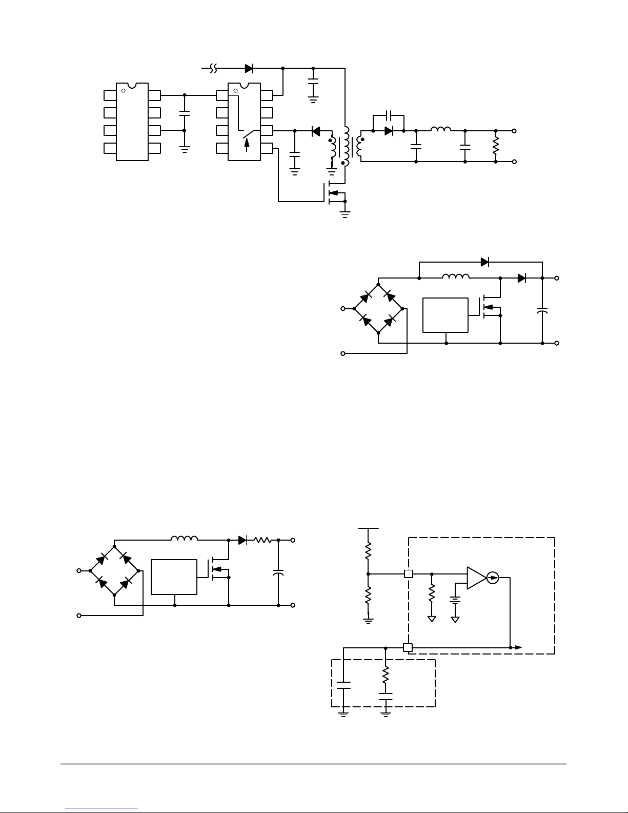
1
2
3
4
NCP1608
NCP1608BOOSTGEVB
D
+
C
PFC(VCC)
88
+
7
6
5
1
2
3
4
NCP1230
7
V
CC
6
+
5
Figure 8. Using the SMPS Controller to Supply Power to the NCP1608
bulk
+
+
+
−
DESIGN STEP 8: Limit the Inrush Current
The sudden application of the ac line voltage to the PFC
pre−converter causes an inrush current and a resonant
voltage overshoot that is several times the normal value.
Resizing the power components to handle inrush current and
a resonant voltage overshoot is cost prohibitive.
1. External Inrush Current Limiting Resistor
A NTC (negative temperature coefficient) thermistor
connected in series with the diode limits the inrush current
(Figure 9). The resistance of the NTC decreases from a few
ohms to a few milliohms as the NTC is heated by the I
2
power dissipation. However, an NTC resistor may not be
sufficient to protect the inductor and C
from inrush
bulk
current during a brief interruption of the ac line voltage, such
as during ac line dropout and recovery.
2. Startup Bypass Rectifier
A rectifier is connected from V
in
to V
(Figure 10). This
out
bypasses the inductor and diverts the startup current directly
to C
bulk
. C
is charged to the peak ac line voltage without
bulk
resonant overshoot and without excessive inductor current.
After startup, D
is reverse biased and does not interfere
bypass
with the boost converter.
NTC
+
V
out
Vac
V
in
NCP1608
D
bypass
V
in
+
NCP1608
Vac
V
out
Figure 10. Use a Second Diode to Route the
R
Inrush Current Away from the Inductor
DESIGN STEP 9: Develop the Compensation Network
The pre−converter is compensated to ensure stability over
the input voltage and output power range. To compensate the
loop, a compensation network is connected between the
Control and ground pins. To ensure high PF, the bandwidth
of the loop is set below 20 Hz. A type 2 compensation
network is selected for this design to increase the phase
margin. The type 2 compensation network is shown in
Figure 11.
V
out
R
out1
FB
R
R
out2
FB
E/A
−
+
+
gm
V
REF
Figure 9. Use a NTC to Limit the Inrush Current
Through the Inductor
http://onsemi.com
8
Control
C
COMP
R
COMP1
C
Compensation
Network
COMP1
Figure 11. Type 2 Compensation Network
V
Control
 Loading...