

Page 1
NCP13992MM240WGEVB
Table 1. GENERAL PARAMETERS
Device
Applications
Input Voltage
Nominal Output
Output Power
V
Ripple
NCP1618
AOI,
90 – 265 Vac
12 Vdc / 20 A
240 W
<150 mV @ Full
Efficiency @
Standby Power
Operating
Cooling
Topology
Board size
Convection Open
L
F
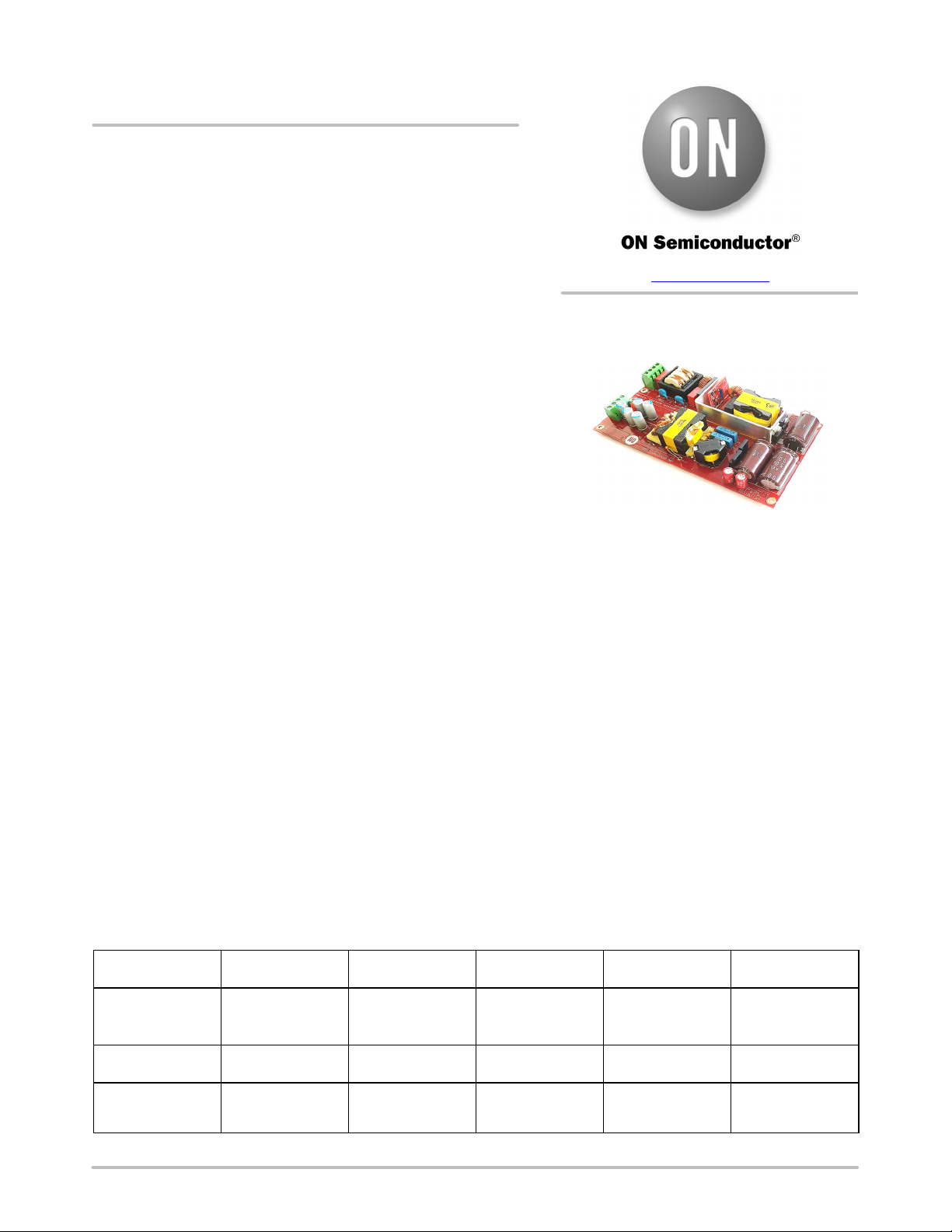
All-in-One Power Supply
Evaluation Board User's
Manual
240 W Power Supply using NCP1618,
www.onsemi.com
NCP13992, NCP4306 and NCP431
Description
This evaluation board user’s manual provides basic information
about a high efficiency, low no−load power consumption reference
design that was tailored to power All−in−One PC or similar type of
equipment that accepts 12 V
implements PFC front stage to assure unity power factor and low
DC on the input. The power supply
THD, current mode LLC power stage to enhance transient response
and secondary side synchronous rectification to maximize efficiency.
This design note provides brief information about controllers’
implementation into design, their interconnections and cooperation.
Please use links in literature section to get detail technical information
about NCP1618, NCP13992, NCP4306 and NCP431.
The NCP1618 is an innovative multimode power factor controller.
The controller automatically change operation mode depending on
conditions so that the efficiency is optimized over the line and load
range. In very light−load conditions, the circuit enters a soft−skip
cycle mode. NCP1618 enters Continuous Conduction Mode (CCM)
under Heavy−Load Conditions, while Frequency−Clamped Critical
Conduction Mode (FCCrM) is used for Medium− and Light−Load
Conditions. PFC−OK Output serves as Brown−Out signal for LLC
controller as well as communication interface which sends NCP1618
into stand−by mode (using Soft−skip cycles).
The NCP13992 is a high performance current mode LLC controller
for half bridge resonant converters. This controller implements 600 V
gate drivers, simplifying layout and reducing external component
count. In applications where a PFC front stage is needed, the
NCP13992 features a dedicated output to drive the PFC controller.
This feature together with quiet skip mode technique further improves
light load efficiency of the whole application. Both controllers provide
a suite of protection features allowing safe power supply operation in
any application. Built−in high voltage input function ease
implementation of the controllers in all applications startup circuits.
EVAL BOARD USER’S MANUA
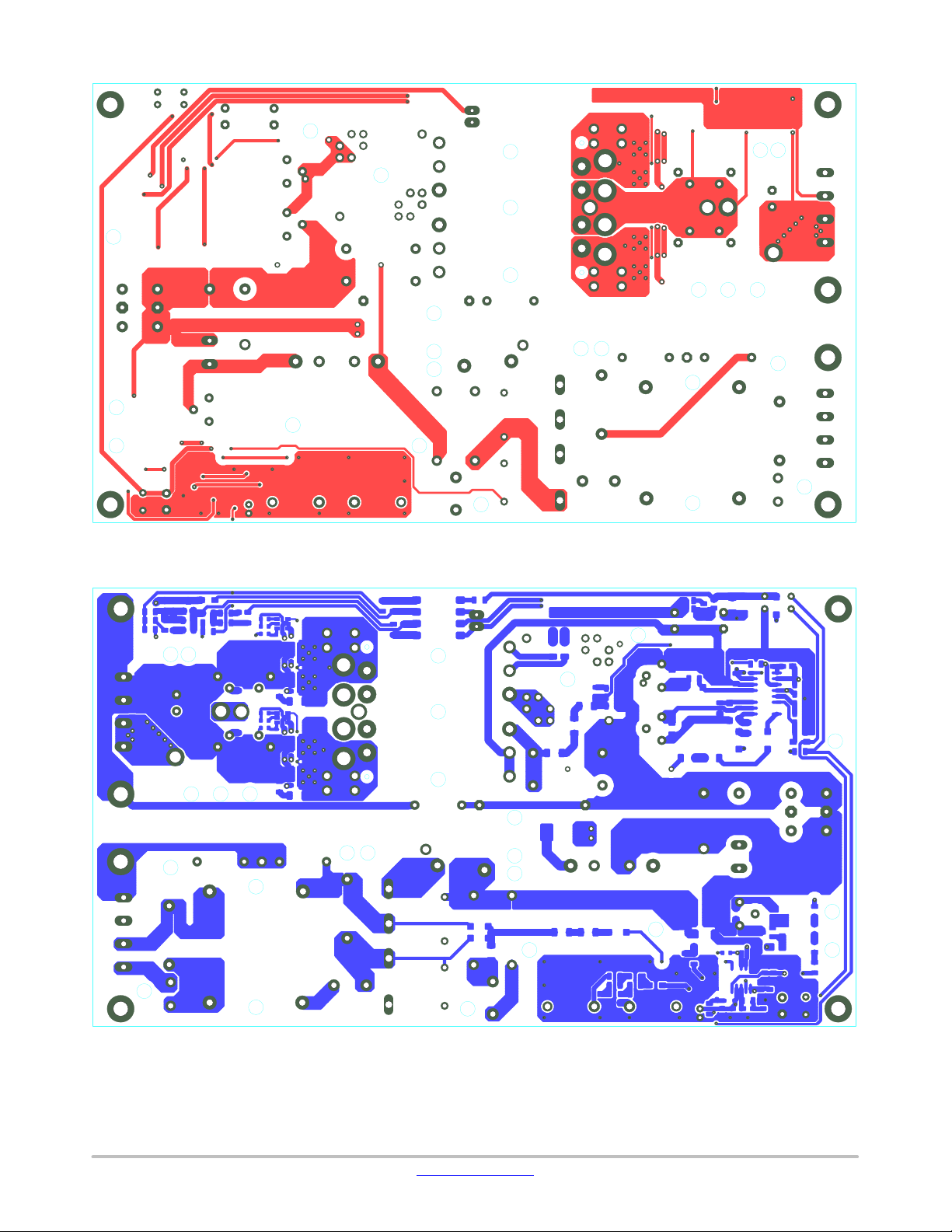
Figure 1. Evaluation Board Photo
eatures
• Wide Input Voltage Range
• PFC Controller with Multimode Operation
• High Efficiency/ Low No−load Power
Consumption
• No Auxiliary SMPS, Fast Startup
• Near Unity Power Factor
• Low Mains & Overload Protection
• Thermal Protection
• Regulated Output Under any Conditions
• Excellent Load & Line Transient Response
• All Magnetics Available as Standard Parts
• Small Form Factor
• Extremely Low No−load Consumption
NCP13992
NCP4306
230 V AC
4 point AVG
94.11%
© Semiconductor Components Industries, LLC, 2020
August, 2020 − Rev. 0
Server Power
Temperature
<130 mW 0 – 40 °C
Voltage / Current
Frame, Forced in
Frame
1 Publication Order Number:
PFC CrCM
LLC + SR
OUT
load
194 × 108 × 27 mm
7.11 W/inch
EVBUM2753/D
3
Page 2
NCP13992MM240WGEVB
E C D_AC
E C D_V C C
E C D_V−
E C D_V+
1 212
6
7
8
HV
10
G ND
DR V
V C C
ZC D
5
C S
4
V M
3
P F C _OK
2
F B
1
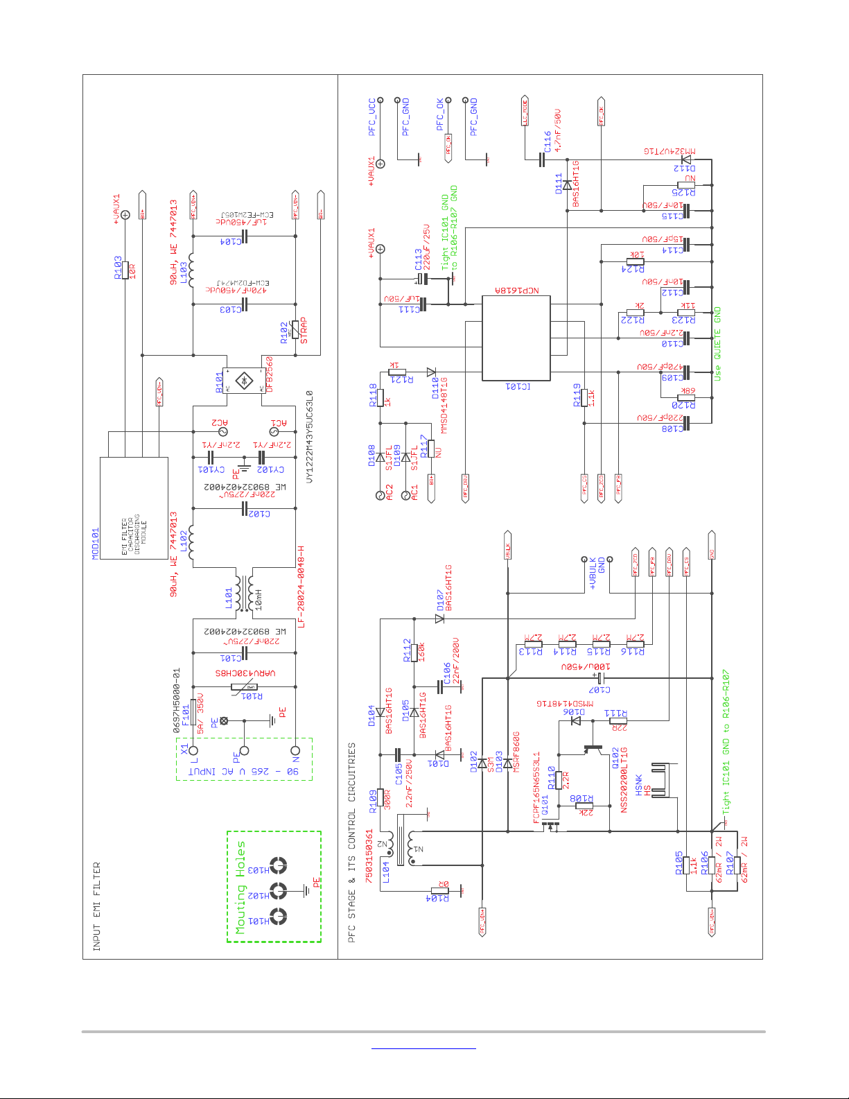
Figure 2. AOI Evaluation Board Schematic − PFC Front Stage
www.onsemi.com
2
Page 3
NCP13992MM240WGEVB
5
6
V C C
MIN_TOF F
DR V1G ND2C S
4
MIN_TON
3
11*2
5*2
1
4
5
6
V C C
MIN_TON
MIN_TOF F
DR V
G ND
C S
1
2
3
12
434
8*2
9*4
3
4
2
16
12
14
11
15
HB
MUP
G ND
MLOW
V B OOT
S K IP4V B /P F C -F B
HV_IN1LLC _C S
LLC _F B
3
6
5
9
10
V C C
MODE
F B _F R E E Z
OV P /OT P
7
8
R
AC
1
2
3
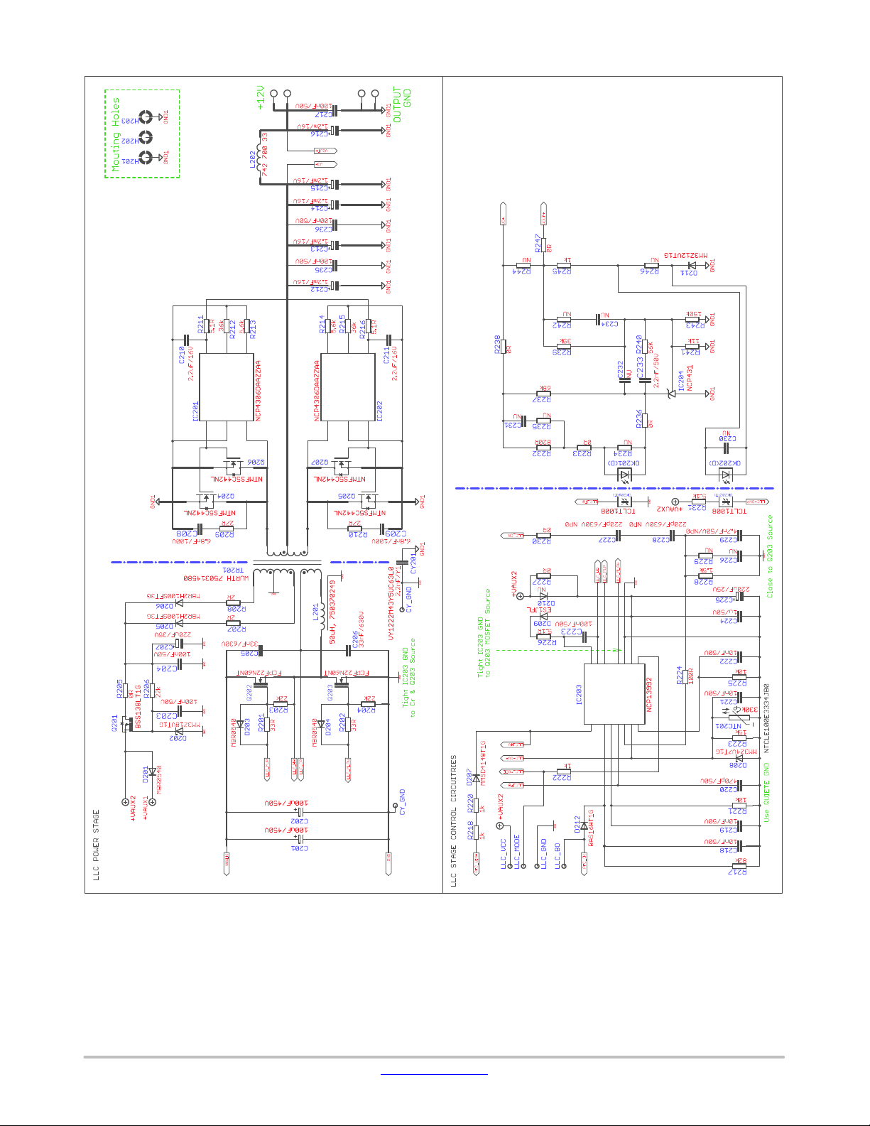
Figure 3. AOI Evaluation Board Schematic − LLC Stage
www.onsemi.com
3
Page 4
NCP13992MM240WGEVB
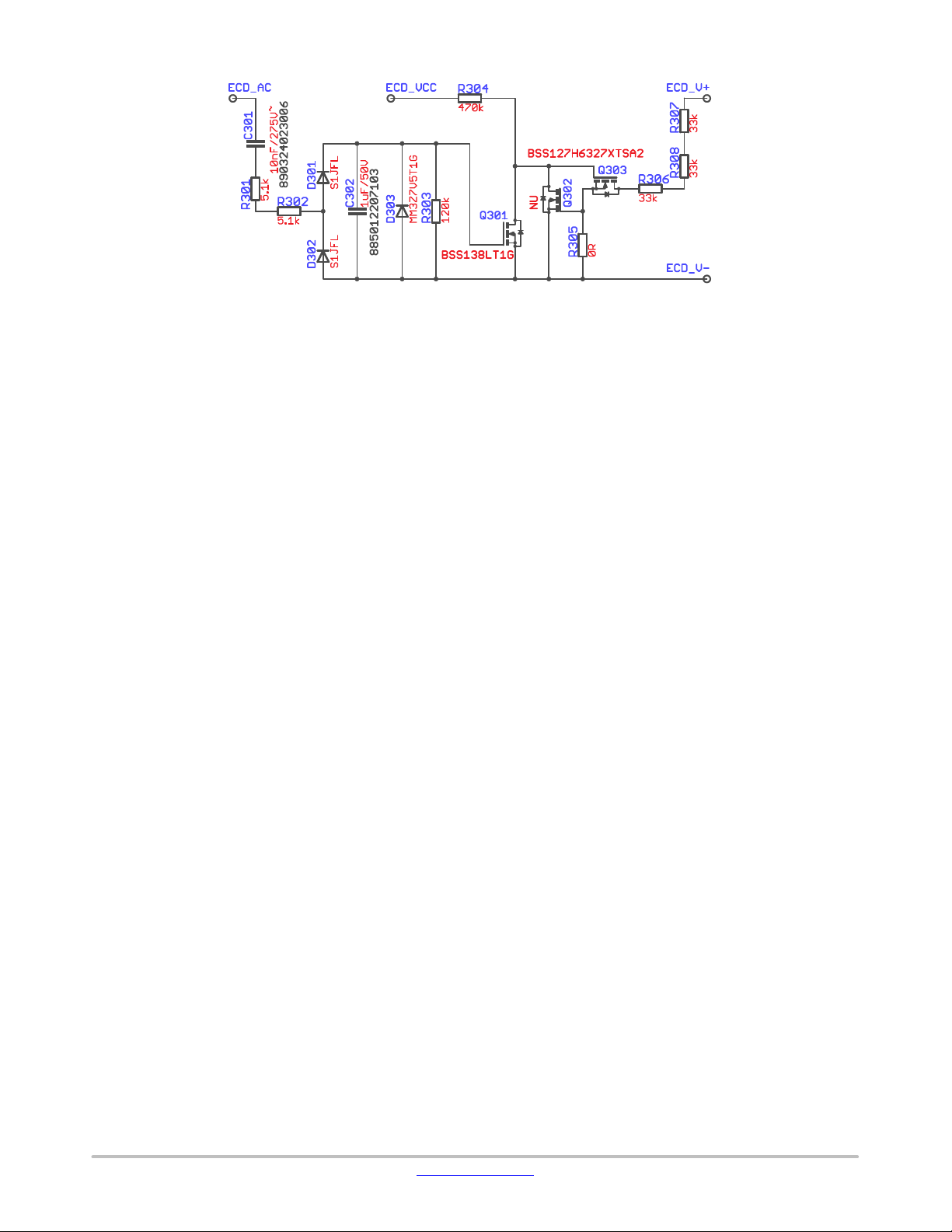
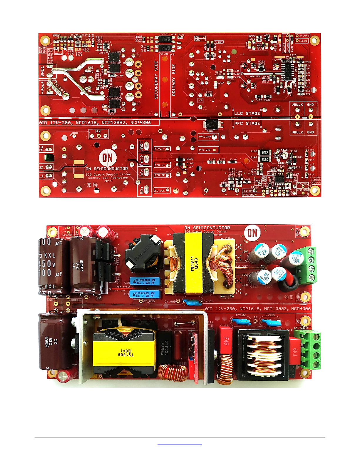
Figure 4. EMI Capacitor Discharging Module (MOD101)
Detailed Descriptions of the Evaluation Board
Input side of evaluation board is protected by a several
components. As first, it’s a 5 A slow reaction fuse F101,
which disconnects input in case wrong manipulation, line
overvoltage stress event and unexpected stresses or
conditions. Voltage dependent resistor R101 serves as input
overvoltage protection triggered at approximately 275 V
AC. Demo−board implements inrush−current limiting
device, R102 NTC thermistor which is not assembled to
allow clear efficiency measurement (Figure 2). It’s
recommended to assemble R102 in case of testing in hard
conditions (using power grid directly or AC power supply
without current limit). Use appropriate NTC inrush current
limiter in case of need.
EMI filter is formed by components L101, L102, L103,
C101, C102, C103, C104, CY101 and CY102 (Figure 2).
The IC101 − NCP1618 measures input line voltage via
diodes D108, D109, D1 10 and resistors R1 18, R121 to detect
present of Brown−out/ Brown−in and SAG conditions as
well as distinguishes input line level. This circuit also
provides PFC Vcc Start−up feature for building controller
Vcc supply. The Power Factor Corrector (PFC) power stage
implements standard boost PFC topology composed of
following power devices; bridge rectifier B101, power
(boost) inductor L104, power MOSFET switch Q101, boost
power diode D103, bypass diode D102, shunt resistors
R106−R107 and bulk capacitors C107, C201−C202. The
PFC controller IC101 (NCP1618) senses input voltage
directly via pin 10 (HV) through network of D108, D109,
D110 and resistors R118, R121. The PFC inductor current
is monitored on the shunt resistor R106−R107. The series
resistors R105−R1 19 set maximum current. Capacitor C108
that is connected between those resistors filters noise caused
by switching. Maximum current through resistors can be
calculated based on NC1618 datasheet. The PFC feedback
divider has high impedance (approximately 10.8 MW)
which ensures low consumption in no−load or light−load
mode conditions. PFC FB divider is created from upper
resistor R113−R116, lower resistor R120 and capacitor
C109. The PFC FB signal is filtered by capacitor C109 to
minimize noise caused by the parasitic capacitive coupling
between pin and other nodes that handle high dV/dt signals.
PFC FB divider sets nominal bulk voltage level which is
400 V approximately. NCP1618 features positive bulk
voltage hiccup, so that while LLC Stage runs under burst
mode, NCP13992 forces NCP1618 to enter skip mode
(stand−by mode), thus bulk−voltage is maintained between
+103% and 98 % of nominal bulk voltage i.e. between
~420 V and ~394 V on this design. NCP1618 can be sent
into soft−skip−mode (stand−by mode) by two ways. This
demo−board implements only one solution – via
pulling−down the PFC−OK pin. Refer to NCP1618
datasheet for more detailed description. Devices D111,
D112, C116 and R222 are used for PFC−OK pulling−down
purpose. Once, IC203 NCP13992 enters to skip, MODE pin
(9) goes low level and pulls down PFC−OK for interval
longer than 29 ms, which results in establishing PFC
stand−by soft skip mode. NCP1618 PFC−OK pin generates
signal which is green−light for down−stream LLC converter .
If no fault occurs and bulk voltage level is in regulation
range, PFC−OK pin sources current which is translated into
drop at R217 and this voltage enables NCP13992 operation.
NCP1618 has integrated driver but the external PNP
transistor Q102 was implemented. The Q102 is connected
directly to source of Q101 in order to minimize discharge
loop and thus allow faster PFC switch turn−off and also
minimizing EMI caused by the driver loop. Q101 Gate
turn−on path is secured by R110, R111 and D106, on the
contrary turn−off path is realized mainly via R1 10 and Q102.
This solution enables to define required switching speeds for
both processes independently. The PFC choke auxiliary
winding voltage is processed by circuit R109, R112, R124,
C105, C106, C114, D10, D104, D105 and D107. Processed
signal is fed into ZCD pin, which detects valleys
zero−current and OVP2 events. This pin provides a voltage
VM for duty cycle modulation when the circuit operates in
continuous conduction mode. The NCP1618 external
network connected to the VM pin adjusts the maximum
power which can be delivered by the PFC stage. R122−R123
set maximum power in CCM mode, C110−C112 filter noise
coupled to this pin.
Schematics diagram in Figure 2 contains module with
designator MOD101. Internal schematic diagram of this
module is displayed in Figure 4. MOD101 was designed as
a part of PFC stage and it’s a discrete solution for discharging
EMI filter differential capacitors. This element was named
as “EMI Capacitor Discharging Module”. Module works in
very simple way based on charge pump principle made of
www.onsemi.com
4
Page 5

NCP13992MM240WGEVB
C301, R301, R302, D301 and D302. When AC voltage is
presented at pin ECD_AC, charge pump creates voltage (at
C302/R303) which is clamped by Zener−diode D303. This
voltage turn−on MOSFET Q301, which pull−down Gate
voltage of Q303. While AC line is presented charge pump
continues to operate and generates voltage/current which
disables Q303. Once, AC line turns out, charge pump stops
and Q303 is turned on and discharges differential capacitors
in EMI filter (through bridge rectifier B101).
Entire LLC power stage is displayed in Figure 3. Power
stage at primary side of LLC converter is composed of these
devices: MOSFETs Q202, Q203, external resonant inductor
L201, transformer TR201 and resonant capacitors C205 and
C206. The IC203 NCP13992, LLC controller senses
primary current indirectly, via resonant capacitor voltage,
which is divided down by a capacitive divider, using
capacitors C227−C228 and C229. The capacitive divider
has to be optimally loaded and in the same time assure fast
signal stabilization after application startup. This is
achieved by resistor R228. Scaled signal from CS divider
passes through resistor R224 which limits maximum current
that can flow into the LLC_CS pin. The FB optocoupler
OK201 is connected to the LLC_FB pin and defines
converter output voltage by pulling down this pin when
lower output power is needed. Capacitor C220 forms high
frequency pole in FB loop characteristics and helps to
eliminate eventual noise that could be coupled to the FB pin
by parasitic coupling paths. The VB/PFC−FB pin allows
LLC converter operation once input level is approximately
above 1.1 V. VB/PFC−FB signal is provided by PFC
controller NCP1618, which sources current from PFC−OK
pin as aforementioned. VB/PFC−FB pin voltage is filtered
by C218. The Skip/REM pin of the NCP13992 is sued for
skip threshold adjustment. Resistor R221 is used for this
purpose together with noise filtering capacitor C219. The
over−voltage and over−temperature protections are
implemented via OVP/OTP pin by using resistor R223,
temperature dependent resistor NTC201, Zener−diode
D208, filtering capacitor C221 and optocoupler OK202.
Simple OVP detector is located on the secondary side and it’s
made of resistor R245, Zener−diode D211 OK202
optocoupler diode. The FB_FREEZE pin (8) defines
minimum internal feedback voltage (lower saturation level),
which influences maximum switching frequency. Resistor
R225 sets FB freeze level and C222 decouples noise. The
PFC stand−by mode (or PFC soft−skip) is activated by
MODE pin ( 9 ) , w hich goes high during LLC stage switching
and stays low during idle mode– as described in PFC section.
The VCC decoupling capacitor C224 and also bootstraps
capacitor C223 for high side driver powering are located as
close to the LLC controller package as possible to minimize
parasitic inductive coupling to other IC adjust components
due to high driver current peaks that are present in the circuit
during drivers rising and falling edge transitions. The
bootstrap capacitor is charged via HV bootstrap diode D209
and series resistor R226 which limits charging current and
VBOOT to HB power supply slope during initial C223
charging process. The gate driver currents are reduced by
added series resistors R201, R202 to optimize EMI signature
of the application. Schottky diodes D203 and D204 are used
to speed−up the MOSFETs turn−off process. The primary
controllers are biased by voltage limiter circuitry, which is
used in order to not exceed VCC pin maximum ratings. The
upper value of the primary VCC voltage is clamped to
approximately 15 V. The VCC clamp is composed of these
components: R205, R206, Q201, D202 and C203. The VCC
clamp is fed from auxiliary windings via rectifier
D205−D206 and current limiting resistor R207−R208. The
secondary side synchronous rectification uses IC201 and
IC202 NCP4306 SR controllers. Two MOSFTEs are
connected in parallel for each SR channel to achieve low
total voltage drop − Q204, Q206 and Q205, Q207. RC
snubber circuits C208−R209 and C209−R210 are used to
damp down the parasitic ringing and thus limit the
maximum peak voltage on the SR MOSFETs. The SR
controllers are supplied from converter output via resistors
R211 and R216. These resistors with decoupling capacitors
C210 and C211 form RC filter. The minimum on−time –
R213, R214 and minimum off−time – R212, R215 resistors
define needed blanking periods that help to overcome SR
controllers false triggering to ringing in the SR power stage.
Each SR controller implements clever light load detection
feature LLD. After first incoming pulse from skip burst, the
LLD feature wakes−up the controller from low power mode
(50 mA). SR controller enters to stand−by mode after defined
period of time (68 ms) once the last pulse from the skip burst
ends. Internal setup cares about LLD feature timing thus
eliminates need for complicated external light−load guard
circuitry. The NCP4306 LLD feature offers great benefits
compare to the traditional solutions, in which SR operation
and no−load consumption is much less efficient. The output
filtering capacitor bank composes from low ESR
electrolytic capacitors C212 to C215 and ceramic capacitors
C217, C235 and C236. Output filter L202, C216 is used to
smooth output voltage from switching glitches. The output
voltage of the converter is regulated by standard shunt
regulator NCP431− IC204. The regulation optocoupler
OK201 is driven via resistor R232 which defines loop gain.
The NCP431 is biased via resistor R237 in case there is no
current flowing via regulation optocoupler –which can
happen before the nominal V
level is reached or during
OUT
transients from no−load to full−load conditions. The output
voltage is adjusted by divider R239, R241, and R243. The
feedback loop compensation network is formed partially by
resistor R240 and capacitor C233.
PCB layout is prepared with options so user can modify
demo−board accordingly if needed – please refer to
schematics. The PCB consists of a 2 layer FR4 board with
70 mm copper thickness to minimize resistance in secondary
side where high currents are conducted. Leaded components
are assembled form the top side of the board and all SMT
components are place from the bottom only. The board was
designed to work as open frame with natural air flow
cooling. Forced air flow cooling management should be
considered in case the board is packed into some box or
target application.
www.onsemi.com
5
Page 6
NCP13992MM240WGEVB
0
0
R
R
0
R
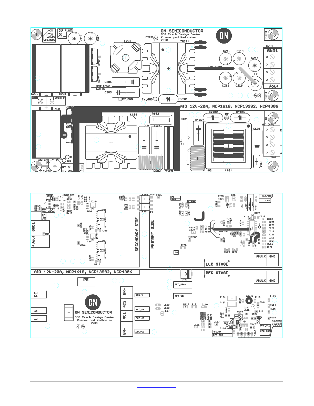
Figure 5. Evaluation Board − Top Side Components
−4+4
4321 4321
Figure 6. Evaluation Board − Bottom Side Components
www.onsemi.com
6
Page 7
NCP13992MM240WGEVB
Figure 7. Evaluation Board − PCB Design of Top Layer
Figure 8. Evaluation Board − PCB Design of Bottom Layer
www.onsemi.com
7
Page 8
NCP13992MM240WGEVB
Figure 9. Evaluation Board Photograph − Bottom Side
Figure 10. Evaluation Board Photograph − Top Side
www.onsemi.com
8
Page 9
NCP13992MM240WGEVB
Figure 11. EMI Capacitor Discharging Module (MOD101) − PCB Layout Design, Assembling, Photographs
www.onsemi.com
9
Page 10
NCP13992MM240WGEVB
96
95
94
93
92
91
90
89
Efficiency [%]
88
87
86
85
84
20 40 60 80 100 120 140 160 180 200 220 240
Output Power [W]
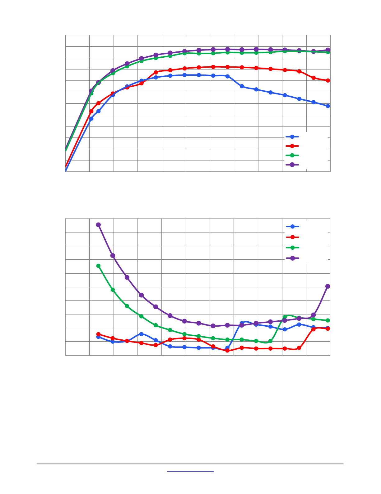
Figure 12. EFFICIENCY vs. Output Power
90 V AC
110 V AC
230 V AC
265 V AC
20
90 V AC
18
16
14
12
10
THD [%]
8
6
4
2
0
20 40 60 80 100 120 140 160 180 200 220 240
Output power [W]
110 V AC
230 V AC
265 V AC
Figure 13. Input Current vs. Output Power
www.onsemi.com
10
Page 11
1.00
0.95
0.90
THD [%]
NCP13992MM240WGEVB
0.85
0.80
20 40 60 80 100 120 140 160 180 200 220 240
Output Power [W]
90 V AC
110 V AC
230 V AC
265 V AC
Figure 14. POWER FACTOR vs. Output Power
160
140
120
100
80
110 V AC
230 V AC
60
Vout pk−pk Ripple [mV]
40
20
0 20 40 60 80 100 120 140 160 180 200 220 240
Output Power [W]
Figure 15. Output Voltage Ripple (pk−pk) vs. Output Power
www.onsemi.com
11
Page 12

NCP13992MM240WGEVB
Table 2. EFFICIENCY DATA MEASURED AND AVERAGED FROM 10 BUILT EVALUATION BOARDS
Consumption [mW] or Efficiency [%]
@ 110 V AC
@ 230 V AC
@ 265 V AC
NO−LOAD
< 110
< 120
< 130
Load 120 mW
< 250
< 250
< 260
Load 500 mW
< 660
< 670
< 680
Load 20% − 4 A
90.02
91.80
91.85
Load 25% − 5 A
91.40
92.65
92.88
Load 50% − 10 A
93.07
94.40
94.57
Load 75% − 15 A
93.11
94.45
94.75
Load 100% − 20 A
92.01
94.51
94.69
4 point AVG
92.40
94.00
94.22
LOAD
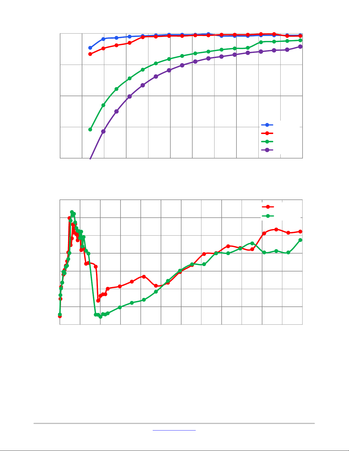
The following figures illustrate conduced EMI signatures
under full loading for different input line voltage levels.
80
EMI signature, V
70
60
50
Amplitude [dBmV]
40
30
20
0.1 1.0 10.0
= 110 Vac, P
IN
Frequency [MHz]
OUT
= 240 W
Quasi−peak Limit
110 V (L−N) MAX PEAK
Figure 16. EMI Signature Comparison @ 110 VAC & Full−load (measured MAX Peak)
www.onsemi.com
12
Page 13

NCP13992MM240WGEVB
EMI signature, V
80
70
60
50
40
Amplitude [dBmV]
30
20
0.1 1.0 10.0
= 230 Vac, P
IN
Frequency [MHz]
OUT
= 240 W
Quasi−peak Limit
230 V (L−N) MAX PEAK
Figure 17. EMI Signature Comparison @ 230 VAC & Full−load (measured MAX Peak)
Evaluation Demo−board Connections and Power−up
and
Test Procedure
IMPORTANT NOTES:
• Do not apply extreme voltage to the input terminals!
• Be careful, high DC voltage is presented!
• Do not apply DC voltage to the input terminals!
• The demo is not optimized for surge, lightning, etc.
• This reference board requires thermal management
especially at very low line voltage. Use fan for
excessive heat spreading.
• Follow up power−up and power−down sequences.
Power−up sequence:
1. Connect AC Supply to the demoboard AC input.
2. Connect Electronic Load at the output terminals
with proper polarity
3. Set AC Supply voltage in range 85 to 265V AC.
4. Turn AC Supply on.
5. Check output terminals voltage, approximately
12 V.
6. Modify electronic load current to desired level
while output voltage is monitored.
Power−down sequence:
1. Turn AC Supply off.
2. Discharge bulk capacitor for manipulating further
www.onsemi.com
13
Page 14

NCP13992MM240WGEVB
CH1
CH2
CH3
CH4
Figure 18. 110 V AC/ STEP LOAD 0 – 20 A
CH1
CH2
CH3
CH4
Figure 19. 110 V AC/ STEP LOAD 20 – 0 A
OPERATING WAVEFORM
V
MLOWER
V
Out_AC
VHB (t)
I
out
(t)
(t)
(t)
V
MLOWER
V
Out_AC
VHB (t)
I
out
(t)
(t)
(t)
www.onsemi.com
14
Page 15

NCP13992MM240WGEVB
CH1
CH2
CH3
CH4
Figure 20. 110 V AC/ STEP LOAD 2 A – 20 A
CH1
CH2
CH3
CH4
Figure 21. 110 V AC/ STEP LOAD 20 A – 2 A
V
MLOWER
V
Out_AC
VHB (t)
I
out
(t)
(t)
(t)
V
MLOWER
V
Out_AC
VHB (t)
I
out
(t)
(t)
(t)
www.onsemi.com
15
Page 16

NCP13992MM240WGEVB
CH1
CH2
CH3
CH4
Figure 22. 110 V AC/ LLC SKIP MODE, No−load
CH1
CH2
CH3
CH4
Figure 23. 110 V AC/ LLC SKIP MODE, No−load − detailed view
V
MLOWER
V
LLC_FB
VHB (t)
I
prim
(t)
(t)
(t)
V
MLOWER
V
LLC_FB
VHB (t)
I
prim
(t)
(t)
(t)
www.onsemi.com
16
Page 17

NCP13992MM240WGEVB
CH1
CH2
CH3
CH4
Figure 24. 110 V AC/ LLC NORMAL MODE, LOAD 3.15 A
CH1
CH2
CH3
CH4
Figure 25. 110 V AC/ LLC NORMAL MODE, LOAD 5 A
V
MLOWER
V
LLC_FB
VHB (t)
I
prim
(t)
(t)
(t)
V
MLOWER
V
LLC_FB
VHB (t)
I
prim
(t)
(t)
(t)
www.onsemi.com
17
Page 18

NCP13992MM240WGEVB
CH1
CH2
CH3
CH4
Figure 26. 110 V AC/ LLC NORMAL MODE 10 A
CH1
CH2
CH3
CH4
Figure 27. 110 V AC/ LLC NORMAL MODE, LOAD 20 A
V
MLOWER
V
LLC_FB
VHB (t)
I
prim
(t)
(t)
(t)
V
MLOWER
V
LLC_FB
VHB (t)
I
prim
(t)
(t)
(t)
www.onsemi.com
18
Page 19

NCP13992MM240WGEVB
CH1
CH2
CH3
CH4
Figure 28. 110 V AC/ LLC START−UP into 0 A
CH1
CH2
CH3
CH4
Figure 29. 110 V AC/ LLC START−UP into 2 A
V
MLOWER
V
Out
VHB (t)
I
prim
(t)
(t)
(t)
V
MLOWER
V
Out
VHB (t)
I
prim
(t)
(t)
(t)
www.onsemi.com
19
Page 20

NCP13992MM240WGEVB
CH1
CH2
CH3
CH4
Figure 30. 110 V AC/ LLC START−UP into 5 A
CH1
CH2
CH3
CH4
Figure 31. 110 V AC/ LLC START−UP into 10 A
V
MLOWER
V
Out
VHB (t)
I
prim
(t)
(t)
(t)
V
MLOWER
V
Out
VHB (t)
I
prim
(t)
(t)
(t)
www.onsemi.com
20
Page 21

NCP13992MM240WGEVB
CH1
CH2
CH3
CH4
Figure 32. 110 V AC/ LLC START−UP into 20 A
CH1
CH2
CH3
CH4
Figure 33. 90 V AC/ Load 20 A, PFC START−UP (No inrush limiter)
V
MLOWER
V
Out
VHB (t)
I
prim
(t)
(t)
(t)
V
Line
V
PFC_Vcc
V
Bulk
I
line
(t)
(t)
(t)
(t)
www.onsemi.com
21
Page 22

CH1
V
CH2
CH3
CH4
Figure 34. 110 V AC/ Load 20 A, PFC START−UP (No inrush limiter)
CH1
CH2
CH3
CH4
Figure 35. 230 V AC/ Load 20 A, PFC START−UP (No inrush limiter)
Line
NCP13992MM240WGEVB
(t)
V
PFC_Vcc
V
Bulk
I
line
V
Line
(t)
(t)
(t)
(t)
V
PFC_Vcc
V
(t)
(t)
Bulk
I
(t)
line
www.onsemi.com
22
Page 23

CH1
Q101 VGS (t)
CH2
CH3
CH4
Figure 36. 90 V AC/ Load 20 A, PFC/ LLC START−UP (No inrush limiter)
CH1
CH2
CH3
CH4
Figure 37. 110 V AC/ Load 20 A, PFC/ LLC START−UP (No inrush limiter)
V
(t)
out
V
(t)
Bulk
I
(t)
line
NCP13992MM240WGEVB
Q101 VGS (t)
V
(t)
out
V
(t)
Bulk
I
(t)
line
www.onsemi.com
23
Page 24

CH1
Q101 VGS (t)
CH2
CH3
CH4
Figure 38. 230 V AC/ Load 20 A, PFC/ LLC START−UP (No inrush limiter)
CH1
CH2
CH3
CH4
Figure 39. 90 V AC/ Load 13 A, PFC CrM MODE – before entering CCM
V
(t)
out
V
(t)
Bulk
NCP13992MM240WGEVB
I
(t)
line
Q101 VGS (t)
IC101 V
(t)
M
Q101 VDS (t)
I
(t)
L103
www.onsemi.com
24
Page 25

CH1
Q101 VGS (t)
CH2
CH3
CH4
Figure 40. 90 V AC/ Load 14 A, PFC CCM MODE
CH1
CH2
CH3
CH4
Figure 41. 90 V AC/ Load 20 A, PFC CCM MODE
NCP13992MM240WGEVB
IC101 V
(t)
M
Q101 VDS (t)
I
(t)
L103
Q101 VGS (t)
IC101 V
(t)
M
Q101 VDS (t)
I
(t)
L103
www.onsemi.com
25
Page 26

CH1
Q101 VGS (t)
CH2
CH3
CH4
Figure 42. 110 V AC/ Load 18 A, PFC CrM MODE – before entering CCM
CH1
CH2
CH3
CH4
Figure 43. 110 V AC/ Load 20 A, PFC CCM MODE
NCP13992MM240WGEVB
IC101 V
(t)
M
Q101 VDS (t)
I
(t)
L103
Q101 VGS (t)
IC101 V
(t)
M
Q101 VDS (t)
I
(t)
L103
www.onsemi.com
26
Page 27

CH1
Q101 VGS (t)
CH2
CH3
CH4
Figure 44. 230 V AC/ Load 20 A, PFC CrM MODE
CH1
CH2
CH3
CH4
Figure 45. 265 V AC/ Load 18 A, PFC CrM MODE
NCP13992MM240WGEVB
IC101 V
(t)
M
Q101 VDS (t)
I
(t)
L103
Q101 VGS (t)
IC101 V
(t)
M
Q101 VDS (t)
I
(t)
L103
www.onsemi.com
27
Page 28

CH1
Q101 VGS (t)
CH2
CH3
CH4
Figure 46. 90 V AC/ Load slowly rising through margin (13 / 14 A), PFC Transition from CrM to CCM
CH1
CH2
CH3
CH4
Figure 47. 90 V AC/ Load slowly decreasing through margin (14/ 13 A), PFC Transition from CCM to CrM
NCP13992MM240WGEVB
IC101 V
(t)
M
Q101 VDS (t)
I
(t)
L103
Q101 VGS (t)
IC101 V
(t)
M
Q101 VDS (t)
I
(t)
L103
www.onsemi.com
28
Page 29

NCP13992MM240WGEVB
CH1
CH2
CH3
CH4
Figure 48. 110 V AC/ No−load, PFC Soft−skip mode − V
Hiccups
CH1
CH2
CH3
CH4
Figure 49. 110 V AC/ No−load, PFC Soft−skip mode − V
Hiccups/ PFC Burst detail
IC101 V
IC203 V
V
Bulk
I
line
PFC_OK
(t)
MODE
(t)
(t)
(t)
Bulk
V
V
Line
Out
N/A
I
line
(t)
(t)
(t)
Bulk
www.onsemi.com
29
Page 30

CH1
V
CH2
CH3
CH4
Figure 50. 90 V AC/ Load 20 A, Hold−up time for 5% regulation – 20 ms
CH1
CH2
CH3
CH4
Figure 51. 110 V AC/ Load 20 A, Hold−up time for 5% regulation – 20 ms
V
Line
Out
N/A
I
Out
NCP13992MM240WGEVB
(t)
(t)
(t)
V
V
Line
Out
N/A
I
Out
(t)
(t)
(t)
www.onsemi.com
30
Page 31

CH1
V
CH2
CH3
CH4
Figure 52. 230 V AC/ Load 20 A, Hold−up time for 5% regulation – 20 ms
CH1
CH2
CH3
CH4
Figure 53. 265 V AC/ Load 20 A, Hold−up time for 5% regulation – 20 ms
V
Line
Out
N/A
I
Out
NCP13992MM240WGEVB
(t)
(t)
(t)
V
V
Line
Out
N/A
I
Out
(t)
(t)
(t)
www.onsemi.com
31
Page 32

NCP13992MM240WGEVB
Literature
High−Voltage, Multimode Power Factor Controller
NCP1618: https://www.onsemi.com/pub/Collateral/NCP1618−D.PDF
High Performance Current Mode Resonant Controller with Integrated High Voltage Drivers:
NCP13992: https://www.onsemi.com/pub/Collateral/NCP13992−D.PDF
Secondary Side Synchronous Rectifier Controllers:
NCP4306: https://www.onsemi.com/pub/Collateral/NCP4306−D.PDF
Voltage Reference, Programmable Shunt Regulator
NCP431: https://www.onsemi.com/pub/Collateral/NCP431−D.PDF
N−Channel SupreMOS® MOSFET 600 V, 22 A, 165 mW
FCPF22N60NT: https://www.onsemi.com/pub/Collateral/FCPF22N60NT−D.pdf
Power Rectifier, Soft Recovery, Switch−mode, 8 A, 600 V
MSRF860G: https://www.onsemi.com/pub/Collateral/MSR860−D.PDF
N−Channel SupreMOS® MOSFET 600 V, 13 A, 258 mW
FCPF165N65S3L1: https://www.onsemi.com/pub/Collateral/FCPF165N65S3L1−D.PDF
Single N−Channel Power MOSFET 40 V, 130 A, 2.5 mW
NVMFS5C442NL: https://www.onsemi.com/pub/Collateral/NVMFS5C442NL−D.PDF
SUPREMOS is a registered trademark of Semiconductor Components Industries, LLC (SCILLC) or its subsidiaries in the United States and/or other countries.
www.onsemi.com
32
Page 33

Table 3. BILL OF MATERIALS
Parts
Qty
Value
Package
Description
Manufacturer
Part Number
Substitution
MAIN BOARD
C101,
C102
2
220nF/275V~
C102−064X133
CAPACITOR
Wurth
890324024002
Not allowed
C1031470nF/450Vdc
C150−072X183
CAPACITOR
Panasonic
ECW−FD2W474J
Not allowed
C10411uF/450Vdc
C150−072X183
MPP CAPACITOR
Panasonic
ECW−FE2W105J
Not allowed
C10512.2nF/250V
C0805
CAPACITOR
Wurth
885342007005
Not allowed
C106122nF/200V
C0805
CAPACITOR
Wurth
885342207006
Not allowed
C107,
3
100u/450V
EC_18X30_7.5
CAPACITOR
United Chemi−Con
EKXL451ELL101MM30S
Allowed
C1081220pF/50V
C0805
CAPACITOR
Wurth
885012007059
Allowed
C109,
2
470pF/50V
C0805
CAPACITOR
Wurth
885012007061
Allowed
C110,
2
2.2nF/50V
C0805
CAPACITOR
Wurth
885012007065
Allowed
C111,
2
1uF/50V
C0805
CAPACITOR
Wurth
885012207103
Allowed
C112,
6
10nF/50V
C0805
CAPACITOR
Wurth
885012207092
Allowed
C113,
2
220uF/25V
E3.5−8
CAPACITOR
Wurth
860040474004
Allowed
C114115pF/50V
C0805
CAPACITOR
Wurth
885012007052
Allowed
C11614.7nF/50V
C0805
CAPACITOR
Wurth
885012007067
Allowed
C203,
3
100nF/50V
C0805
CAPACITOR
Wurth
885012207098
Allowed
C2041100nF/50V
C1206
CAPACITOR
Wurth
885012208087
Allowed
C205,
2
33nF/630V
C150−064X183
CAPACITOR
Epcos
B32652A6333J
Allowed
C2071220uF/35V
E3,5−8
CAPACITOR
Wurth
860010574011
Allowed
C208,
2
6.8nF/100V
C0805
CAPACITOR
Wurth
885012207121
Allowed
C210,
2
2.2uF/16V
C0603
CAPACITOR
Wurth
885012106018
Allowed
C212,
5
1.2mF/16V
E3.5−8
CAPACITOR
United Chemi−Con
APSG160ELL122MH20S
Not allowed
C227,
2
220pF/630V NP0
C1206
CAPACITOR
KEMET
C1206C221JBGACAUTO
Not allowed
C22914.7nF/50V/NP0
C0805
CAPACITOR
Wurth
885012007067
Not allowed
CY101,
3
2.2nF/Y1
YC10B5
Y CAPACITOR
Murata
DE1E3KX222MN4AP01F
Not allowed
F10115A/ 350V SLOW
0697H
FUSE
Bel Fuse
0697H5000−01
Allowed
L101110mH
LF−280XX
COMMON MODE
ICE
LF−28024−0048−H
Not allowed
L102,
2
90uH
TO18
DIF. MODE
Wurth
7447013
Not allowed
L1041260uH
PQ32/20−4
PFC INDUCTOR
Sumida
T91869
7503150361
L201150uH
RM8
Resonant inductor
Sumida
T91870
750370249
L20211 turn
FERRITE BEAD
POWER FERRITE
Wurth
74270033
Not allowed
NTC2011330k, 5%
THT
NTC
Vishay
NTCLE100E3334JB0
Allowed
R1011275 VAC
LITTELFUSE
VARISTOR
Littelfuse
V430CH8S
Not allowed
R1021STRAP
N/A
NTC THERMISTOR
N/A
N/A
N/A
R103110R
R0603
RESISTOR
VARIOUS
VARIOUS
Allowed
NCP13992MM240WGEVB
C201,
C202
C220
C233
C224
C115,
C218,
C219,
C221,
C222
C225
C217,
C223,
C235,
C236
C206
C209
C211
Electrolytic
Electrolytic
Electrolytic
C213,
C214,
C215,
C216
C228
CY102,
CY201
L103
09X05
POLYMER
INDUCTOR
INDUCTOR
BEAD
www.onsemi.com
33
COMPONENTS
Page 34

Table 3. BILL OF MATERIALS (continued)
R104,
60RR0805
RESISTOR
VARIOUS
VARIOUS
Allowed
R105,
2
1.1k
R0805
RESISTOR
VARIOUS
VARIOUS
Allowed
R106,
2
62m / 2W
R6332W
RESISTOR
TE Connectivity /
RLP73N3AR062JTE
Similar type
R108,
4
22k
R0805
RESISTOR
VARIOUS
VARIOUS
Allowed
R1091300R
R0805
RESISTOR
VARIOUS
VARIOUS
Allowed
R11012.2R
R0805
RESISTOR
VARIOUS
VARIOUS
Allowed
R111122R
R0805
RESISTOR
VARIOUS
VARIOUS
Allowed
R1121160k
R0805
RESISTOR
VARIOUS
VARIOUS
Allowed
R113,
4
2.7M 1%
R0805
RESISTOR
ROHM
KTR18EZPF2704
Similar type
R118,
41kR1206
RESISTOR
VARIOUS
VARIOUS
Allowed
R120,
2
68k
R0805
RESISTOR
TE Connectivity /
CRGCQ0805F68K
Similar type
R12212k
R0805
RESISTOR
VARIOUS
VARIOUS
Allowed
R123,
2
11k
R0805
RESISTOR
VARIOUS
VARIOUS
Allowed
R124,
3
10k
R0805
RESISTOR
VARIOUS
VARIOUS
Allowed
R201,
2
33R
R0805
RESISTOR
VARIOUS
VARIOUS
Allowed
R207,
22RR1206
RESISTOR
VARIOUS
VARIOUS
Allowed
R209,
2
27R
R1206
RESISTOR
VARIOUS
VARIOUS
Allowed
R211,
2
5.1R
R0603
RESISTOR
VARIOUS
VARIOUS
Allowed
R212,
2
36k
R0603
RESISTOR
VARIOUS
VARIOUS
Allowed
R213,
2
5.6k
R0603
RESISTOR
VARIOUS
VARIOUS
Allowed
R217182k
R0805
RESISTOR
VARIOUS
VARIOUS
Allowed
R222,
21kR0805
RESISTOR
VARIOUS
VARIOUS
Allowed
R223115k
R0805
RESISTOR
VARIOUS
VARIOUS
Allowed
R2241100R
R0805
RESISTOR
VARIOUS
VARIOUS
Allowed
R22615.1R
R0805
RESISTOR
VARIOUS
VARIOUS
Allowed
R227,
20RR1206
RESISTOR
VARIOUS
VARIOUS
Allowed
R22811.5k
R0805
RESISTOR
VARIOUS
VARIOUS
Allowed
R23115.1k
R0805
RESISTOR
VARIOUS
VARIOUS
Allowed
R2321820R
R0805
RESISTOR
VARIOUS
VARIOUS
Allowed
R239139k
R0805
RESISTOR
VARIOUS
VARIOUS
Allowed
R240156k
R0805
RESISTOR
VARIOUS
VARIOUS
Allowed
R2431150k
R0805
RESISTOR
VARIOUS
VARIOUS
Allowed
TR2011600uH/ n = 16
PQ3220
LLC TRANSFORMER
Sumida
T91871
Not allowed
X101,
4
Pitch 5.08 mm
WR−TBL Series 2365
SCREW TERMINAL
Wurth
691236510002
Allowed
C226,
5
NOT USED
C0805
CAPACITOR
N/A
N/A
N/A
R1171NOT USED
R1206
RESISTOR
N/A
N/A
N/A
Parts SubstitutionPart NumberManufacturerDescriptionPackageValueQty
R205,
R233,
R236,
R238,
R247
R119
NCP13992MM240WGEVB
R107
R203,
R204,
R206
R114,
R115,
R116
R121,
R218,
R220
R237
R241
R221,
R225
R202
R208
R210
Holsworthy
Smiconductor
Holsworthy
R216
R215
R214
R245
R230
X201
C230,
C231,
C232,
C234
www.onsemi.com
34
Page 35

Table 3. BILL OF MATERIALS (continued)
R125,
7
NOT USED
R0805
RESISTOR
N/A
N/A
N/A
B1011DFB2560
SIP−4
Bridge Rectifier
ON Semiconductor
DFB2560
Not allowed
D201,
3
MBR0540
SOD123
DIODE
ON Semiconductor
MBR0540
Similar type
D101,
6
BAS16HT1G
SOD323
DIODE
ON Semiconductor
BAS16HT1G
Similar type
D1021S3M
SMC
DIODE
ON Semiconductor
S3M
Similar type
D1031MSRF860G
TO−220−2 FullPak
POWER DIODE
ON Semiconductor
MSRF860G
Similar type
D106,
3
MMSD4148T1G
SOD123
DIODE
ON Semiconductor
MMSD4148T1G
Similar type
D108,
2
S1JFL
SOD123
DIODE
ON Semiconductor
S1JFL
Allowed
D112,
2
MM3Z4V7T1G
SOD323
ZENER DIODE
ON Semiconductor
MM3Z4V7T1G
Not allowed
D2021MM3Z18VT1G
SOD323
ZENER DIODE
ON Semiconductor
MM3Z18VT1G
Not allowed
D205,
2
MBR2H100SFT3G
SOD123
DIODE
ON Semiconductor
MBR2H100SFT3G
Not allowed
D2091ES1JFL
SOD123
DIODE
ON Semiconductor
ES1JFL
Not allowed
D2111MM3Z12VT1G
SOD323
ZENER DIODE
ON Semiconductor
MM3Z12VT1G
Not allowed
IC1011NCP1618A
SO10
PFC CONTROLLER
ON Semiconductor
NCP1618A
Not allowed
IC201,
2
NCP4306
TSOP6
SR DRIVER
ON Semiconductor
NCP4306DAAZZAA
Not allowed
IC2031NCP13992
SO16
LLC CONTROLLER
ON Semiconductor
NCP13992
Not allowed
IC2041NCP431
SOT23
SHUNT REGULATOR
ON Semiconductor
NCP431BISNT1G
Not allowed
OK201,
2
TCLT1008
SOP−4
OPTOCOUPLER
VISHAY
TCLT1008
Not allowed
Q1011FCPF165N65S3L1
TO−220−2 FullPak
POWER MOSFET
ON Semiconductor
FCPF165N65S3L1
FCPF22N60N
Q1021NSS20200LT1G
SOT23
NPN Transistor
ON Semiconductor
NSS20200LT1G
Similar type
Q2011BSS138LT1G
SOT23
MOSFET
ON Semiconductor
BSS138LT1G
Similar type
Q202,
2
FCPF22N60NT
TO−220−2 FullPak
POWER MOSFET
ON Semiconductor
FCPF22N60NT
Similar type
Q204,
4
NTMFS5C442NL
SO8FL
POWER MOSFET
ON Semiconductor
NTMFS5C442NLT1G
Similar type
D2101NOT USED
SOD123
DIODE
N/A
N/A
N/A
MOD101 − EMI FIL TER CAPACITOR DISCHARGING MODULE
Parts
Qty
Value
Package
Description
MANUFACTURER
PART NUMBER
Substitution
C301110nF/275V~
C102−043X133
MPP CAPACITOR
Wurth
890324023006
Allowed
C30211uF/50V
C0805
CAPACITOR
Wurth
885012207103
Similar type
D301,
2
S1JFL
SOD123
DIODE
ON Semiconductor
S1JFL
Not allowed
D3031MM3Z7V5T1G
SOD323
ZENER DIODE
ON Semiconductor
MM3Z7V5T1G
Not allowed
Q3011BSS138LT1G
SOT23
MOSFET
ON Semiconductor
BSS138LT1G
Similar type
Q3031BSS127
SOT23
MOSFET
Infineon
BSS127H6327XTSA2
Not allowed
R301,
2
5.1k
R0805
RESISTOR
VARIOUS
VARIOUS
Allowed
R3031120k
R0805
RESISTOR
VARIOUS
VARIOUS
Allowed
R3041470k
R0805
RESISTOR
VARIOUS
VARIOUS
Allowed
R30510R
R0805
RESISTOR
VARIOUS
VARIOUS
Allowed
R306,
3
33k
R0805
RESISTOR
VARIOUS
VARIOUS
Allowed
Q3021NOT USED
SOT23
MOSFET
N/A
N/A
N/A
Parts SubstitutionPart NumberManufacturerDescriptionPackageValueQty
R229,
R234,
R235,
R242,
R244,
R246
D203,
D204
D104,
D105,
D107,
D111,
D212
D110,
D207
D109
D208
NCP13992MM240WGEVB
D206
IC202
OK202
Q203
Q205,
Q206,
Q207
D302
T
R302
R307,
R308
www.onsemi.com
35
Page 36

ON Semiconductor and the ON Semiconductor logo are trademarks of Semiconductor Components Industries, LLC dba ON Semiconductor or its subsidiaries in the United States and/or
other countries. ON Semiconductor owns the rights to a number of patents, trademarks, copyrights, trade secrets, and other intellectual property. A listing of ON Semiconductor’s
product/patent coverage may be accessed at www.onsemi.com/site/pdf/Patent−Marking.pdf
subject to all applicable copyright laws and is not for resale in any manner.
The evaluation board/kit (research and development board/kit) (hereinafter the “board”) is not a finished product and is as such not available for sale to consumers. The board is only intended
for research, development, demonstration and evaluation purposes and should as such only be used in laboratory/development areas by persons with an engineering/technical training
and familiar with the risks associated with handling electrical/mechanical components, systems and subsystems. This person assumes full responsibility/liability for proper and safe handling.
Any other use, resale or redistribution for any other purpose is strictly prohibited.
The board is delivered “AS IS” and without warranty of any kind including, but not limited to, that the board is production−worthy, that the functions contained in the board will meet your
requirements, or that the operation of the board will be uninterrupted or error free. ON Semiconductor expressly disclaims all warranties, express, implied or otherwise, including without
limitation, warranties of fitness for a particular purpose and non−infringement of intellectual property rights.
ON Semiconductor reserves the right to make changes without further notice to any board.
You are responsible for determining whether the board will be suitable for your intended use or application or will achieve your intended results. Prior to using or distributing any systems
that have been evaluated, designed or tested using the board, you agree to test and validate your design to confirm the functionality for your application. Any technical, applications or design
information or advice, quality characterization, reliability data or other services provided by ON Semiconductor shall not constitute any representation or warranty by ON Semiconductor,
and no additional obligations or liabilities shall arise from ON Semiconductor having provided such information or services.
The boards are not designed, intended, or authorized for use in life support systems, or any FDA Class 3 medical devices or medical devices with a similar or equivalent classification in
a foreign jurisdiction, or any devices intended for implantation in the human body. Should you purchase or use the board for any such unintended or unauthorized application, you shall
indemnify and hold ON Semiconductor and its officers, employees, subsidiaries, affiliates, and distributors harmless against all claims, costs, damages, and expenses, and reasonable
attorney fees arising out of, directly or indirectly, any claim of personal injury or death associated with such unintended or unauthorized use, even if such claim alleges that ON Semiconductor
was negligent regarding the design or manufacture of the board.
This evaluation board/kit does not fall within the scope of the European Union directives regarding electromagnetic compatibility, restricted substances (RoHS), recycling (WEEE), FCC,
CE or UL, and may not meet the technical requirements of these or other related directives.
FCC WARNING – This evaluation board/kit is intended for use for engineering development, demonstration, or evaluation purposes only and is not considered by ON Semiconductor to
be a finished end product fit for general consumer use. It may generate, use, or radiate radio frequency energy and has not been tested for compliance with the limits of computing devices
pursuant to part 15 of FCC rules, which are designed to provide reasonable protection against radio frequency interference. Operation of this equipment may cause interference with radio
communications, in which case the user shall be responsible, at its expense, to take whatever measures may be required to correct this interference.
ON Semiconductor does not convey any license under its patent rights nor the rights of others.
LIMITATIONS OF LIABILITY: ON Semiconductor shall not be liable for any special, consequential, incidental, indirect or punitive damages, including, but not limited to the costs of
requalification, delay, loss of profits or goodwill, arising out of or in connection with the board, even if ON Semiconductor is advised of the possibility of such damages. In no event shall
ON Semiconductor’s aggregate liability from any obligation arising out of or in connection with the board, under any theory of liability, exceed the purchase price paid for the board, if any.
For more information and documentation, please visit www.onsemi.com
.
. ON Semiconductor is an Equal Opportunity/Affirmative Action Employer. This literature is
PUBLICATION ORDERING INFORMATION
LITERATURE FULFILLMENT:
Email Requests to: orderlit@onsemi.com
ON Semiconductor Website: www.onsemi.com
TECHNICAL SUPPORT
North American Technical Support:
Voice Mail: 1 800−282−9855 Toll Free USA/Canada
Phone: 011 421 33 790 2910
Europe, Middle East and Africa Technical Support:
Phone: 00421 33 790 2910
For additional information, please contact your local Sales Representative
◊
www.onsemi.com
1
 Loading...