

NCP1397A, NCP1397B
查询"NCP1397-D"供应商
High Performance Resonant
Mode Controller with
Integrated High--Voltage
Drivers
The NCP1397 is a high performance controller that can be utilized
in half bridge resonant topologies such as series resonant, parallel
resonant and LLC resonant converters. It integrates 600 V gate
drivers, simplifying layout and reducing external component count.
With its unique architecture, including a 500 kHz Voltage Controlled
Oscillator whose control mode permits flexibility when an ORing
function is required, the NCP1397 delivers everything needed to build
a reliable and rugged resonant mode power supply.
The NCP1397 provides a suite of protection features with
configurable settings to optimize any application. These include:
auto--recovery or fault latch--off, brown--out, open optocoupler,
soft--start and short--circuit protection. Deadtime is also adjustable to
overcome shoot through current.
Features
High--Frequency Operation from 50 kHz up to 500 kHz
600 V High--Voltage Floating Driver
Adjustable Minimum Switching Frequency with ±3% Accuracy
Adjustable Deadtime from 100 ns to 2 ms.
Startup Sequence Via an Externally Adjustable Soft--Start
Brown--Out Protection for a Simpler PFC Association
Latched Input for Severe Fault Conditions, e.g. Over Temperature or
OVP
Timer--Based Input with Auto--Recovery Operation for Delayed
Event Reaction
Latched Overcurrent Protection
Disable Input for Immediate Event Reaction or Simple ON/OFF
Control
V
Low Startup Current of 300 mA
1 A / 0.5 A Peak Current Sink / Source Drive Capability
Common Collector Optocoupler Connection for Easier ORing
Optional Common Emitter Optocoupler Connection
Internal Temperature Shutdown
These Devices are Pb--Free, Halogen Free/BFR Free and are RoHS
Operationupto20V
CC
Compliant
http://onsemi.com
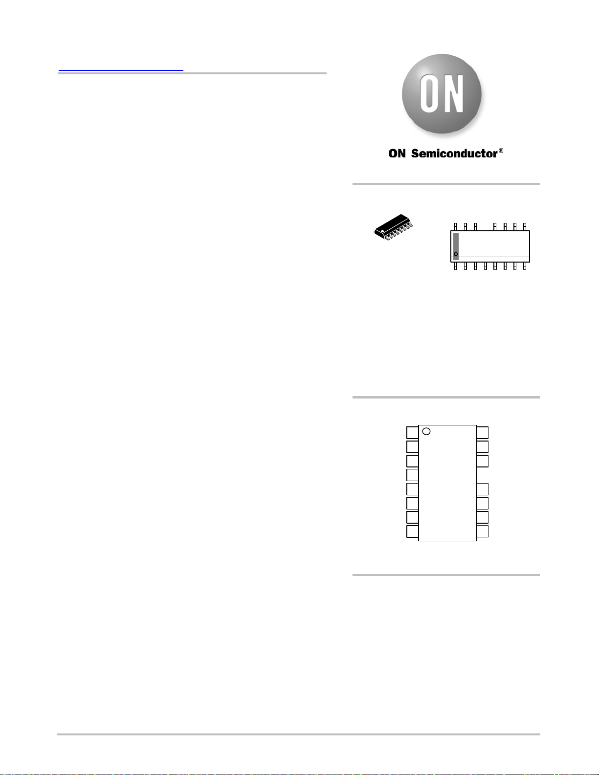
MARKING
DIAGRAMS
16
SO--16, LESS PIN 13
Skip/Disable
See detailed ordering and shipping information in the package
dimensions section on page 26 of this data sheet.
1
D SUFFIX
CASE 751AM
x=AorB
A = Assembly Location
WL = Wafer Lot
Y = Year
WW = Work Week
G = Pb--Free Package
PIN CONNECTIONS
CSS(dis)
Ctimer
1
Fmax
2
3
Rt
4
BO
5
FB
6
DT
7
8
ORDERING INFORMATION
16
1
(Top View)
NCP1397xG
AWLYWW
Vboot
16
Mupper
15
HB
14
V
12
CC
Mlower
11
GND
10
Fault
9
Typical Applications
Flat Panel Display Power Converters
High Power ac--dc Adapters for Notebooks
Computing Power Supplies
Semiconductor Components Industries, LLC, 2010
November, 2010 -- Rev. 2
Industrial and Medical Power Sources
Offline Battery Chargers
1 Publication Order Number:
NCP1397/D
查询"NCP1397-D"供应商
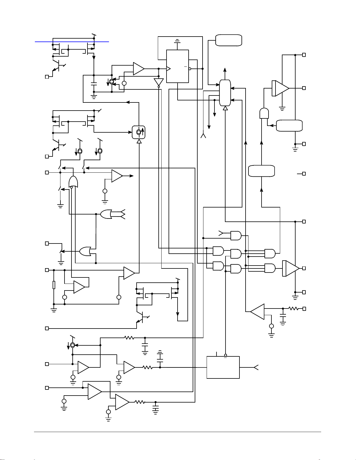
R18
NCP1397A, NCP1397B
Figure 1. Typical Application Example
PIN FUNCTION DESCRIPTION
Pin # Pin Name Function Pin Description
1 CSS(dis) Soft--Start Discharge Soft--start capacitor discharge pin. Connect to the soft--start capacitor to reset it
2 Fmax Maximum frequency clamp A resistor sets the maximum frequency excursion
3 Ctimer Timer duration Sets the timer duration in presence of a fault
4 Rt Minimum frequency c lamp Connecting a resistor to this pin, sets the minimum oscillator frequency reached
5 BO Brown--Out Detects low input voltage conditions. When brought above V
6 FB Feedback Injecting current into this pin increases the oscillation frequency up to Fmax.
7 DT Deadtime A simple resistor adjusts the dead-- time width
8 Skip/Disable Skip or Disable input Upon release, a clean startup sequence occurs if VFB< 0.3 V. During the skip
9 Fault Fault detection input When asserted, the external timer starts to countdown and shuts down the
10 GND Analog ground --
11 Mlower Low side output Drives the lower side MOSFET
12 V
13 NC Not c onnected Increases the creepage distance
14 HB Half--bridge connection Connects to the half--bridge output
15 Mupper High side output Drives the higher side MOSFET
16 Vboot Bootstrap pin ThefloatingVCCsupply for the upper stage
CC
Supplies the controller Thecontrolleracceptsupto20V
before startup or during overload conditions.
=1V.
for V
FB
(4 V typically), it
fully latches off the controller.
mode, when FB doesn’t drop below 0.3 V, the IC restarts without soft--start
sequence.
controller at the end of its time duration. Simultaneously the Soft--Start discharge
switch is activated so the converter operating frequency goes up to protect
application power stage. This input features also second fault comparator with
higher threshold (1.5 V typically) that:
A) Speeds up the timer capacitor charging current 8 times – NCP1397A
B) latches off the IC permanently – NCP1397B
In both versions the second fault comparator helps to protect application in case
of short circuit on the output or transformer secondary winding.
latch
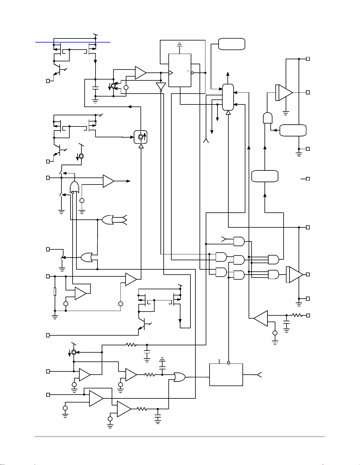
http://onsemi.com
2
NCP1397A, NCP1397B
查询"NCP1397-D"供应商
VDD
Imin
VFB VFB(off)
Vref
Rt
I = Imax for Vfb = 5.3 V
I = 0 for Vfb < Vfb(min)
Fmax
Time r
VDD
Vref
C
Itimer1
IDT
VDD
Imax
VFB = 5
Vdd
Itimer2
Temperature
Shutdown
S
D
Q
+
--
+
DT Adj.
+
--
+
Vref
Timeout
Fault
Clk
Q
R
50% DC
PON
Reset
Fault
Timeout
Fault
Vref
Management
VCC
FF
BO
Reset
Fast
Fault
Level
Shifter
UVLO
V
BOOT
Mupper
HB
NC
SS(dis)
FB
RFB
DT
BO
IBO
+
--
+
VFB(fault)
VDD
+
IDT
+
--
VBO
PON
Reset
Fault
G=1
+
--
+
VFB(min)
20 msNoise
Filter
+
--
+
Vlatch
> 0 only
V=V(FB)-- VFB(min)
Vref
20 msNoise
Filter
VDD
Deadtime
Adjustment
S
Fault
V
CC
Mlower
GND
Filter
Skip/
Disable
--
+
Vref Skip/Disable
Q
Q
R
PON Reset
20 ns Noise
+
Fault
+
Vref(fault)
+
--
Vref( OCP )
+
--
+
1 msNoise
Filter
Figure 2. Internal Circuit Architecture (NCP1397A)
http://onsemi.com
3
NCP1397A, NCP1397B
查询"NCP1397-D"供应商
VDD
Imin
Itimer1
+
Vref
C
VFB VFB(off)
IDT
VDD
Imax
Vfb = 5
+
--
Rt
I = Imax for Vfb = 5.3 V
I = 0 for Vfb < Vfb_min
Fmax
Time r
Vref
Vref
VDD
Vref
If FAULT Itimer else 0
+
+
--
DT Adj.
Time out
Fault
Temperature
Shutdown
S
D
Q
PON
Reset
Fault
Timeout
Fault
Vref
Management
VCC
FF
BO
Reset
Fast
Fault
Level
Shifter
UVLO
Clk
Q
R
50% DC
V
BOOT
Mupper
HB
NC
SS(dis)
FB
DT
BO
Fault
RFB
IBO
+
+
VFB(fault)
VDD
+
+
Vref(fault)
--
IDT
+
--
VBO
+
--
Vref( OCP )
PON
Reset
Fault
Fault
G=1
+
+
--
+
VFB(min)
20 msNoise
Filter
+
--
+
Vlatch
+
--
> 0 only
V=V(FB)-- VFB(min)
Vref
20 msNoise
Filter
1 msNoise
Filter
VDD
Deadtime
Adjustment
Q
Q
S
Figure 3. Internal CircuitArchitecture (NCP1397B)
V
CC
Mlower
GND
Filter
Skip/
Disable
--
+
Vref Skip
R
PON Reset
20 ns Noise
+
http://onsemi.com
4
NCP1397A, NCP1397B
MAXIMUM RATINGS
查询"NCP1397-D"供应商
Rating Symbol Valu e Unit
High Voltage bridge pin, pin 14 V
Floating supply voltage, ground referenced V
High side output voltage V
Low side output voltage V
Allowable output slew rate dV
Power Supply voltage, pin 12 V
BOOT
BRIDGE
-- V
BRIDGE
DRV(HI)
DRV(LO)
/dt 50 V/ns
BRIDGE
CC
Maximum voltage, all pins (except pin 11 and 10) -- --0.3to10 V
Thermal Resistance Junction--to--Air, PDIP version
Thermal Resistance Junction--to--Air, SOIC version
R
θ
JA
R
θ
JA
Storage Temperature Range -- -- 60 to +150 C
ESD Capability, Human Body Model (HBM) (All pins except HV pins) -- 2 kV
ESD Capability, Machine Model (MM) -- 200 V
Stresses exceeding Maximum Ratings may damage the device. Maximum Ratings are stress ratings only. Functional operation above the
Recommended Operating Conditions is not implied. Extended exposure to stresses above the Recommended Operating Conditions may affect
device reliability.
1. This device(s) contains ESD protection and exceeds the following tests:
Human Body Model 2000 V per JEDEC Standard JESD22--A114E
Machine Model 200 V per JEDEC Standard JESD22--A115--A
2. This device meets latchup tests defined by JEDEC Standard JESD78.
--1to600 V
0to20 V
V
BRIDGE
V
BOOT
-- 0 . 3 t o
+0.3
--0.3toVCC+0.3 V
20 V
100 C/W
130 C/W
V
http://onsemi.com
5
NCP1397A, NCP1397B
ELECTRICAL CHARACTERISTICS (For typical values T
查询"NCP1397-D"供应商
= 12 V unless otherwise noted)
Symbol
Rating Pin Min Typ Max Unit
=25C, for min/max values TJ=--40C to +125C, Max TJ= 150C, V
J
CC
SUPPLY SECTION
V
CC(on)
V
CC(min)
V
boot(on)
V
boot(min)
I
startup
V
CC(reset)VCC
I
CC1
I
CC2
I
CC3
Turn-- on threshold level, VCCgoing up 12 9.7 10.5 11.3 V
Minimum operating voltage after turn--on 12 8.7 9.5 10.3 V
Startup voltage on the floating section 16--14 8 9 10 V
Cutoff voltage on the floating section 16--14 7.4 8.4 9.4 V
Startup current, VCC<V
CC(on)
12 -- -- 300
level at which the internal logic gets reset 12 -- 6.6 -- V
Internal IC consumption, no output load on pin 15/14 – 11/10,
= 300 kHz
F
SW
Internal IC consumption, 1 nF output load on pin 15/14 – 11/10,
= 300 kHz
F
SW
Consumption in fault or disable mode (All drivers disabled,
Rt = 34 kΩ,R
=10kΩ)
DT
12 -- 4 -- mA
12 -- 11 -- mA
12 -- 1.5 -- mA
mA
VOLTAGE CONTROL OSCILLATOR (VCO)
F
SW(min)
F
SW(max)
FB
Minimum switching frequency, Rt = 34 kΩ on pin 4, V
DT = 300 ns
Maximum switching frequency, R
5.3V,Rt=34kΩ, DT = 300 ns
Feedback pin swing above which Δf=0
SW
f(max)
pin6
=1.9kΩ on pin 2, V
=0.8V,
>
pin6
4 58.2 60 61.8 kHz
2 440 500 560 kHz
6 -- 5.3 -- V
DC Operating duty--cycle symmetry 11 --1 5 48 50 52 %
T
T
V
ref(Rt)
del1
del2
Delay before driver restart from fault or disable mode -- -- 700 -- ns
Delay before driver restart after V
event (Note 4) -- -- 11 --
CC(on)
ms
Reference voltage for Rt pin 4 2.18 2.3 2.42 V
FEEDBACK SECTION
R
FB
V
FB(min)
V
FB(off)
V
FBoff(hyste)
Internal pulldown resistor 6 -- 20 --
kΩ
Voltage on pin 6 below which the FB level has no VCO action 6 -- 1.1 -- V
Voltage on pin 6 below which the controller considers the FB fault 6 240 280 320 mV
Feedback fault comparator hysteresis 6 -- 45 -- mV
DRIVE OUTPUT
T
T
R
OH
R
OL
T
dead
T
dead(max)
T
dead(min)
I
HV(LEAK)
Output voltage risetime @ CL= 1 nF, 10--90% of output signal 15-- 14/11-- 10 -- 40 -- ns
r
Output voltage falltime @ CL= 1 nF, 10--90% of output signal 15--14/11--10 -- 20 -- ns
f
Source resistance 15--14/11-- 10 -- 13 --
Sink resistance 15--14/11-- 10 -- 5.5 --
Deadtime with RDT=10kΩ frompin7toGND
Maximum deadtime with RDT=82kΩ frompin7toGND
Minimum deadtime, RDT=3kΩ frompin7toGND
7 250 290 340 ns
7 -- 2 --
7 -- 100 -- ns
Leakage current on high voltage pins to GND 14, 15,16 -- -- 5
Ω
Ω
ms
mA
TIMERS
I
timer1
Timer capacitor charge current during feedback fault or when
V
ref(fault)<Vpin9<Vref(OCP)
3 150 175 190
mA
3. The IC does not activate soft--start (unless the feedback pin voltage is below 0.3 V) when the skip/disable input is released, this is for skip
cycle implementation.
4. Guaranteed by design.
http://onsemi.com
6
NCP1397A, NCP1397B
ELECTRICAL CHARACTERISTICS (For typical values T
查询"NCP1397-D"供应商
= 12 V unless otherwise noted)
=25C, for min/max values TJ=--40C to +125C, Max TJ= 150C, V
J
CC
Symbol UnitMaxTypMinPinRating
TIMERS
I
timer2
T
timer
T
timerR
V
timer(on)
V
timer(off)
R
SS(dis)
Timer capacitor charge current when V
) – A version only
I
charge2
pin9>Vref(OCP)(Icharge1
Timer duration with a 1 mF capacitor anda1MΩ resistor, I
current applied
timer1
+
3 1.1 1.3 1.5 mA
3 -- 24 -- ms
Timer recurrence in permanent fault, same values as above 3 -- 1.4 -- s
Voltage at which pin 3 stops output pulses 3 3.8 4 4.2 V
Voltage at which pin 3 restarts output pulses 3 0.95 1 1.05 V
Soft--start discharge switch channel resistance 1 -- 100 --
Ω
PROTECTION
V
ref(Skip)
Hyste
V
ref(Fault)
Hyste
V
ref(OCP)
Hyste
T
p(Disable)
IBO
(bias)
Reference voltage for Skip/Disable input (Note 4) 8 630 660 690 mV
Hysteresis for Skip/Disable (Note 4) 8 -- 45 -- mV
(Skip)
Reference voltage for Fault comparator 9 0.99 1.04 1.09 V
Hysteresis for fault comparator input 9 -- 60 -- mV
(Fault)
Reference voltage for OCP comparator 9 1.47 1.55 1.63 V
Hysteresis for OCP comparator input 9 -- 90 -- mV
(OCP)
Propagation delay from disable input to the drive shutdown 8 -- 60 100 ns
Brown--Out input bias current 5 -- 0.02 --
mA
VBO Brown--Out level 5 0.99 1.04 1.09 V
IBO Hysteresis current, V
Vl
atch
T
SD
T
SD(hyste)
Latching voltage 5 3.7 4 4.3 V
Temperature shutdown -- 140 -- -- C
Hysteresis -- -- 30 -- C
> VBO 5 25 28 31
pin5
mA
3. The IC does not activate soft--start (unless the feedback pin voltage is below 0.3 V) when the skip/disable input is released, this is for skip
cycle implementation.
4. Guaranteed by design.
http://onsemi.com
7
NCP1397A, NCP1397B
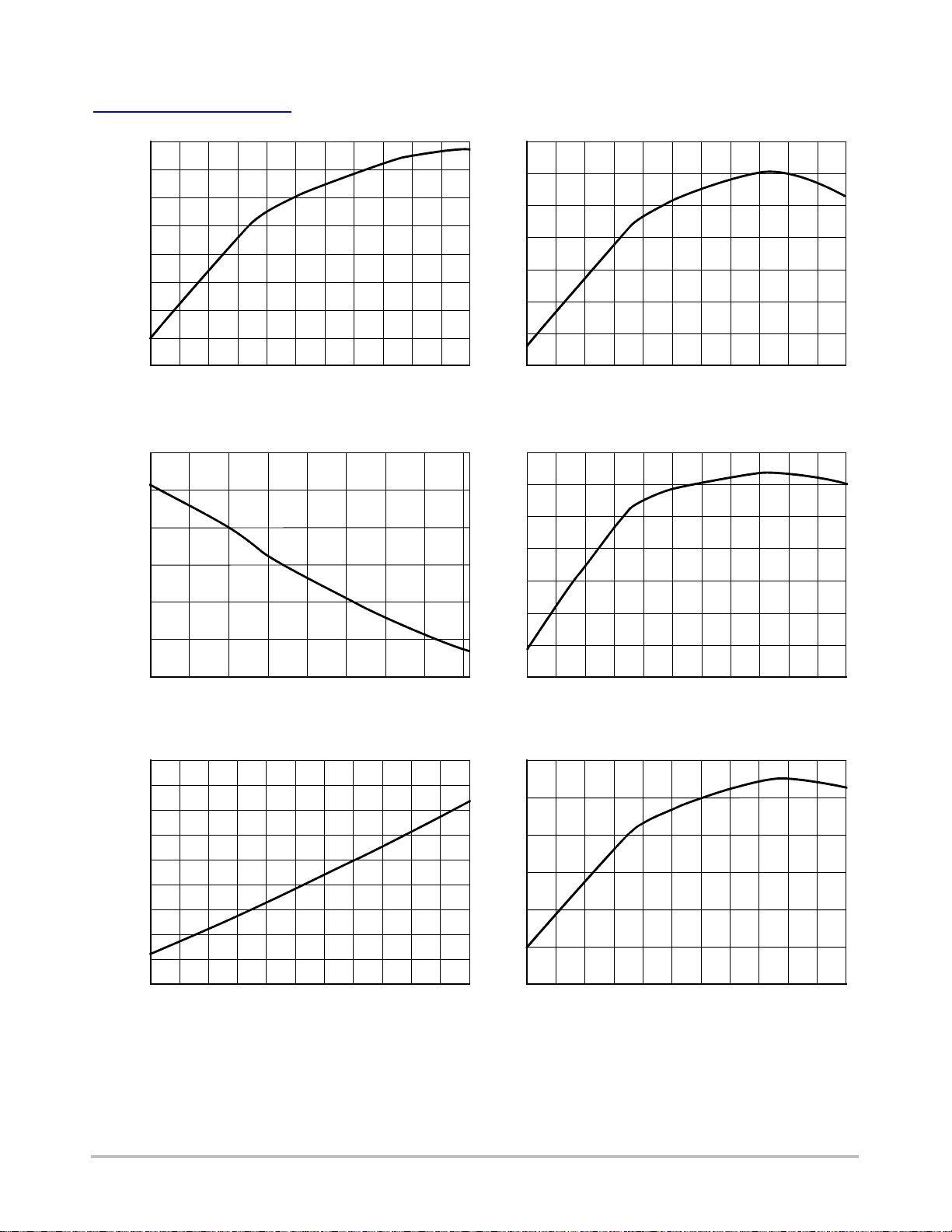
5
p
)
查询"NCP1397-D"供应商
10.55
10.50
(V)
10.45
CC(on)
V
10.40
10.35
--40 --25 --10 5 20 35 50 65 80 95 110 125
TEMPERATURE (C)
Figure 4. V
60.05
60
59.95
(kHz)
59.9
SW(min)
59.85
F
59.8
CC(on)
TYPICAL CHARACTERISTICS
9.52
9.50
9.48
(V)
9.46
9.44
CC(min)
V
9.42
9.40
9.38
Threshold
510
509
508
507
(kHz)
506
SW(max)
F
505
504
--40 --25 --10 5 20 35 50 65 80 95 110 125
TEMPERATURE (C)
Figure 5. V
CC(min)
Threshold
59.75
--40 --20 0 20 40 60 80 100 120
TEMPERATURE (C)
Figure 6. F
23.0
22.5
22.0
21.5
21.0
(kΩ)
20.5
FB
R
20.0
19.5
19.0
18.5
--40 --25 --10 5 20 35 50 65 80 95 110 125
SW(min)
TEMPERATURE (C)
Frequency Clamp
Figure 8. Pulldown Resistor (RFB)
503
--40 --25 --10 5 20 35 50 65 80 95 110 125
TEMPERATURE (C)
Figure 7. F
0.661
0.660
0.659
(V)
0.658
ref(skip)
V
0.657
0.656
0.655
--40 --25 --10 5 20 35 50 65 80 95 110 12
SW(max)
TEMPERATURE (C)
Frequency Clamp
Figure 9. Skip/Disable Threshold (V
ref(ski
)
http://onsemi.com
8
NCP1397A, NCP1397B
查询"NCP1397-D"供应商
17.0
16.0
15.0
14.0
13.0
12.0
ROHA (Ω)
11. 0
10.0
9.0
8.0
--40 --25 --10 5 20 35 50 65 80 95 110 125
TEMPERATURE (C)
TYPICAL CHARACTERISTICS
Figure 10. Source Resistance (ROH)
114
113
112
111
110
(ns)
109
108
dead(min)
T
107
106
105
104
--40 --25 --10 5 20 35 50 65 80 95 110 125
TEMPERATURE (C)
Figure 12. T
dead(min)
9.0
8.5
8.0
7.5
7.0
6.5
6.0
ROLA (Ω)
5.5
5.0
4.5
4.0
--40 --25 --10 5 20 35 50 65 80 95 110 125
TEMPERATURE (C)
Figure 11. Sink Resistance (ROL)
297
296
295
294
293
(ns)
292
291
dead(nom)
290
T
289
288
287
286
--40 --25 --10 5 20 35 50 65 80 95 110 125
TEMPERATURE (C)
Figure 13. T
dead(nom)
2.065
2.060
2.055
(ms)
2.050
dead(max)
2.045
T
2.040
2.035
--40 --25 --10 5 20 35 50 65 80 95 110 125
TEMPERATURE (C)
Figure 14. T
dead(max)
4.035
4.030
4.025
(V)
4.020
latch
V
4.015
4.010
4.005
--40 --25 --10 5 20 35 50 65 80 95 110 125
http://onsemi.com
9
TEMPERATURE (C)
Figure 15. Latch Level (V
latch
)
NCP1397A, NCP1397B
5
)
查询"NCP1397-D"供应商
1.038
1.036
1.034
1.032
1.030
VBO (V)
1.028
1.026
1.024
1.022
--40 --25 --10 5 20 35 50 65 80 95 110 125
TEMPERATURE (C)
Figure 16. Brown--Out Reference (VBO)
1.050
1.048
1.046
1.044
(V)
1.042
1.040
ref(fault)
V
1.038
1.036
1.034
1.032
--40 --25 --10 5 20 35 50 65 80 95 110 125
TEMPERATURE (C)
Figure 18. Fault Input Reference (V
TYPICAL CHARACTERISTICS
28.8
28.6
28.4
28.2
28.0
27.8
IBO (mA)
27.6
27.4
27.2
27.0
--40 --25 --10 5 20 35 50 65 80 95 110 12
Figure 17. Brown--Out Hysteresis Current
178
176
174
(mA)
172
timer1
I
170
168
166
--40 --25 --10 5 20 35 50 65 80 95 110 12
ref(fault)
)
Figure 19. C
TEMPERATURE (C)
(IBO)
TEMPERATURE (C)
1stCurrent (I
timer
timer1
)
1.565
1.560
1.555
(V)
1.550
1.545
ref(OCP)
V
1.540
1.535
1.530
--40 --25 --10 5 20 35 50 65 80 95 110 125
TEMPERATURE (C)
Figure 20. OCP reference (V
ref(OCP
)
1.34
1.33
1.32
1.31
1.30
(mA)
1.29
timer2
I
1.28
1.27
1.26
1.25
--40 --25 --10 5 20 35 50 65 80 95 110 12
TEMPERATURE (C)
Figure 21. C
2ndCurrent (I
timer
timer2
)
http://onsemi.com
10

NCP1397A, NCP1397B
查询"NCP1397-D"供应商
4.035
4.030
4.025
(V)
4.020
timer(on)
V
4.015
4.010
4.005
--40 --25 --10 5 20 35 50 65 80 95 110 125
TEMPERATURE (C)
TYPICAL CHARACTERISTICS
Figure 22. Fault Timer Ending Voltage
(V
timer(on)
)
1.000
0.999
0.288
0.286
0.284
(V)
0.282
0.280
FB(off)
V
0.278
0.276
0.274
--40 --25 --10 5 20 35 50 65 80 95 110 125
TEMPERATURE (C)
Figure 23. FB Fault Detection Threshold
(V
FB(fault)
)
0.998
0.997
(V)
0.996
timer(off)
0.995
V
0.994
0.993
0.992
--40 --25 --10 5 20 35 50 65 80 95 110 125
TEMPERATURE (C)
Figure 24. Fault Timer Reset V oltage (Vt
imer(off)
)
http://onsemi.com
11

NCP1397A, NCP1397B
查询"NCP1397-D"供应商
The NCP1397A/B includes all necessary features to help
building a rugged and safe switch--mode power supply
featuring an extremely low standby power. The below
bullets detail the benefits brought by implementing the
NCP1397A/B controller:
APPLICATION INFORMATION
Wide frequency range: A high--speed Voltage Control
Oscillator allows an output frequency excursion from
50 kHz up to 500 kHz on M
lower
and M
upper
outputs.
Adjustable dead--time: Due to a single resistor wired
to ground, the user has the ability to include some
dead--time, helping to fight cross--conduction between
the upper and the lower transistor.
Adjustable soft--start: Every time the controller starts
to operate (power on), the switching frequency is
pushed to the programmed starting value by external
components (R
toward the minimum frequency, until the feedback loop
closes. The soft--start discharge input (SS(dis))
discharges the Soft--Start capacitor before any IC restart
excluding the restart after Disable is released AND FB
voltage is higher than 0.3 V . The Soft--Start discharge
switch also activates in case the Fault input detects the
overload conditions.
Fmin
//R
) and slowly moves down
Fstart
Adjustable minimum and maximum frequency
excursion: In resonant applications, it is important to
stay away from the resonating peak to keep operating
the converter in the right region. Thanks to a single
external resistor, the designer can program its lowest
frequency point, obtained in lack of feedback voltage
(during the startup sequence or in short--circuit
conditions). Internally trimmed capacitors offer a ±3%
precision on the selection of the minimum switching
frequency. The adjustable upper stop being less precise
to ±12%.
Low startup current: When directly powered from the
high--voltage DC rail, the device only requires 300 mA
to startup.
Brown--Out detection: To avoid operation from a low
input voltage, it is interesting to prevent the controller
from switching if the high--voltage rail is not within the
right boundaries. Also, when teamed with a PFC
front--end circuitry, the brown--out detection can ensure
a clean startup sequence with soft--start, ensuring that
the PFC is stabilized before energizing the resonant
tank. The BO input features a 28 mA hysteresis current
for the lowest consumption.
Adjustable fault timer duration: When a fault is
detected on the Fault input or when the FB path is
broken, timer pin starts to charge an external capacitor.
If the fault is removed, the timer opens the charging
path and nothing happens. When the timer reaches its
selected duration (via a capacitor on Pin 3), all pulses
are stopped. The controller now waits for the discharge
via an external resistor on Pin 3 to issue a new clean
startup sequence via soft--start.
Cumulative fault events: In the NCP1397A/B, the
timer capacitor is not reset when the fault disappears. It
actually integrates the information and cumulates the
occurrences. A resistor placed in parallel with the
capacitor will offer a simple way to adjust the discharge
rate and thus the auto--recovery retry rate.
Overcurrent detection using Fault input: The fault
input is specifically designed to protect LLC
application in case of short circuit or overload. In case
the voltage on this input grows above first threshold the
current source is activated and Fault timer
I
timer
capacitor starts charging. Simultaneously the Soft--Start
discharge switch is activated to increase operating
frequency of the converter. The IC stops operation in
case the Fault timer elapses. The Fault input includes
also second fault comparator that:
-- Speeds up the fault timer capacitor charging by
increasing the I
-- Latches off the device – NCP1397B
The second fault comparator thus helps to protect the power
stage in case of hard short circuit (like shorted transformer
winding etc.)
timer1
current to I
– NCP1397A
timer2
Skip cycle possibility: The absence of the soft--start on
the Skip/Disable input (in case the V
an easy way to implement skip cycle when power
saving features are necessary. A simple resistive divider
from the feedback pin to the Skip/Disable input, and
skip can be implemented.
> 0.3 V) offers
FB
Broken feedback loop detection: Upon startup or any
time during operation, if the FB signal is missing, the
timer starts to charge timer capacitor. If the loop is
really broken, the FB level does not grow--up before the
timer ends charging. The controller then stops all pulses
and waits until the timer pin voltage collapses to 1 V
typically before a new attempt to restart, via the
soft--start. If the optocoupler is permanently broken, a
hiccup takes place.
Common collector or common emitter optocoupler
connection options: This IC allows the designer to
select from two possible optocoupler configurations.
Voltage--Controlled Oscillator
The VCO section features a high--speed circuitryallowing
operation from 100 kHz up to 1 MHz. However,as a division
by two internally creates the two Q and /Q outputs, the final
effective signal on output M
between 50 kHz and 500 kHz. The VCO is configured in
such a way that if the feedback pin voltage goes up, the
switching frequency also goes up. Figure 25 shows the
architecture of the VCO oscillator.
lower
and M
upper
switches
http://onsemi.com
12

NCP1397A, NCP1397B
查询"NCP1397-D"供应商
Rt
Rt sets
Fmin for V(FB) = 0
DT
RDT sets
the deadtime
V
CC
Fmax
Vref
Vref
V
DD
Imin
V
DD
V
DD
0toIFmax
Cint
IDT
Imin
FBinternal
+
--
+
--
+
max
F
max
SW
DSQ
Clk
R
Q
AB
Fmax sets
the maximum F
SW
FB
RFB
20 k
Figure 25. The Simplified VCO Architecture
The designer needs to program the maximum switching
frequency and the minimum switching frequency. In LLC
configurations, for circuits working above the resonant
frequency, a high precision is required on the minimum
frequency, hence the ±3% specification. This minimum
switching frequency is actually reached when no feedback
closes the loop. It can happen during the startup sequence,
a strong output transient loading or in a short--circuit
condition. By installing a resistor from Pin 4 to GND, the
minimum frequency is set. Using the same philosophy,
wiring a resistor from Pin 2 to GND will set the maximum
frequency excursion. To improve the circuit protection
features, we have purposely created a dead zone, where the
feedback loop has no action. This is typically below 1.1 V.
Figure 26 details the arrangement where the internal voltage
(that drives the VCO) varies between 0 and 2.3 V. However,
to create this swing, the feedback pin (to which the
optocoupler emitter connects), will need to swing typically
between 1.1 V and 5.3 V.
+
--
Vb(off)
V
CC
FB
+
R1
11. 3 k
R3
100 k
R2
8.7 k
D1
2.3 V
VFB < VFB(off)
Start f ault timer
+
--
+
Vref
0.5 V
RFmax
Fmax
Figure 26. The OPAMP Arrangement Limits the
VCO Modulation Signal between 0.5 and 2.3 V
http://onsemi.com
13

NCP1397A, NCP1397B
x
)
This techniques allows us to detect a fault on the converter
查询"NCP1397-D"供应商
in case the FB pin cannot rise above 0.3 V (to actually close
the loop) in less than a duration imposed by the
programmable timer. Please refer to the fault section for
detailed operation of this mode.
As shown on Figure 26, the internal dynamics of the VCO
control voltage will be constrained between 0.5 V and 2.3 V,
whereas the feedback loop will drive Pin 6 (FB) between
1.1 V and 5.3 V. If we take the default FB pin excursion
numbers, 1.1 V = 50 kHz, 5.3 V = 500 kHz, then the VCO
maximum slope will be:
500k − 50k
4.2
Figures 27 and 28 portray the frequency evolution
depending on the feedback pin voltage level in a different
frequency clamp combination.
Figure 27. Maximal Default Excursion,
Rt = 34 kΩ onPin4andR
= 107 kHz/V
=1.9kΩ on Pin 2
F(ma
Figure 28. Here a different minimum frequency was
programmed as well as a maximum frequency
excursion
Please note that the previous small--signal VCO slope has
now been reduced to 300k / 4.1 = 71 kHz / V on M
M
outputs. This offers a mean to magnify the feedback
lower
upper
and
excursion on systems where the load range does not generate
a wide switching frequency excursion. Due to this option,
we will see how it becomes possible to observe the feedback
level and implement skip cycle at light loads. It is important
to note that the frequency evolution does not have a real
linear relationship with the feedback voltage. This is due to
the deadtime presence which stays constant as the switching
period changes.
The selection of the three setting resistors (F
max,Fmin
and
deadtime) requires the usage of the selection charts
displayed below:
550
450
VCC=15V
V
=6.5V
FB
DT = 300 ns
(kHz)
350
max
F
250
150
50
1.9 11.9 21.9 31.9 41.9
R
Fmax
F
min
F
(kΩ)
max
= 200 kHz
=50kHz
Figure 29. Maximum Switching Frequency Resistor
Selection Depending on the Adopted Minimum
Switching Frequency
http://onsemi.com
14

NCP1397A, NCP1397B
500
查询"NCP1397-D"供应商
450
400
350
(kHz)
300
min
F
250
200
150
100
2468101214161820
(kΩ)
R
Fmin
VCC=15V
V
FB
DT = 300 ns
Figure 30. Minimum Switching Frequency Resistor
Selection (F
100
90
80
70
(kHz)
60
min
F
50
40
30
20
20 30 40 50 60 70 80 90 100 110
= 100 kHz to 500 kHz)
min
R
(kΩ)
Fmin
VCC=15V
V
FB
DT = 300 ns
Figure 31. Minimum Switching Frequency Resistor
Selection (F
1900
1700
1500
1300
1100
DT (ns)
900
700
500
300
100
3.5 13.5 23.5 33.5 43.5 53.5 63.5 73.5 83.5
= 20 kHz to 100 kHz)
min
RDT(kΩ)
Figure 32. Deadtime Resistor Selection
=1V
=1V
ORing capability and optocoupler connection
configurations
If for any particular reason, there is a need for a frequency
variation linked to an event appearance (instead of abruptly
stopping pulses), then the FB pin lends itself very well to the
addition of other sweeping loops. Several diodes can easily
be used perform the job in case of reaction to a fault event
or to regulate on the output current (CC operation).
Figure 33 shows how to do it.
V
CC
In2
FBIn1
20 k
VCO
Figure 33. Thanks to the FB Configuration, Loop
ORing is Easy to Implement
The VCO configuration used in this IC also offers an easy
way to connect optocoupler (or pulldown bipolar) directly
to the Rt pin instead of FB pin (refer to Figures 34 and 35).
The optocoupler is then configured as “common emitter”
and the operating frequency is controlled by the current that
is taken out from the Rt pin – we have current controller
oscillator (CCO). If one uses this configuration it is needed
to maintain FB pin voltage between 0.3 V and 1 V otherwise
the FB fault will be detected. The FB pin can be still used for
open FB loop detection in some applications – to do so it is
needed to keep optcoupler emitter voltage higher then 0.3 V
for nominal load conditions. One needs to take R
FB
pulldown resistor into account when using this
configuration. It is possible to implement skip mode using
Skip/disable input and emitter resistors R
skip1
and R
skip2
.
http://onsemi.com
15

查询"NCP1397-D"供应商
Figure 34. Feedback Configuration Using Direct Connection to the Rt Pin
NCP1397A, NCP1397B
Fstart(adj) -- RFstart/RFmin
Fmin(adj) -- RFmin
Fmax(adj) -- Rc + Rskip1 + Rskip2
RFstart
RFmin
CSS
Rc
OK1
Rskip1
Rskip2
SS
Fmax
Rt
VCC
FB
GND
Skip/Disable
NCP1397
Fstart(adj) -- RFstart/RFmin
Fmin(adj) -- RFmin
Fmax(adj) -- Rc + Rskip1 + R skip2
RFstart
RFmin
CSS
Rc
OK1
Rskip1
Rskip2
1N4148
Rbias
SS
Fmax
Rt
VCC
FB
GND
Skip/Disable
NCP1397
Figure 35. Feedback Configuration Using Direct Connection to the Rt Pin – No Open FB Loop Detection
Dead--Time Control
Deadtime control is an absolute necessity when the
half--bridge configuration comes to play. The deadtime
technique consists in inserting a period during which both
high and low side switches are off. Of course, the deadtime
amount differs depending on the switching frequency,hence
the ability to adjust it on this controller. The option ranges
between 100 ns and 2 ms. The deadtime is actually made by
controlling the oscillator discharge current. Figure 36
During the discharge time, the clock comparator is high and
invalidates the AND gates: both outputs are low. When the
comparator goes back to the low level, during the timing
capacitor Ct recharge time, A and B outputs are validated.
By connecting a resistor R
to ground, it creates a current
DT
whose image serves to dischargethe Ct capacitor: we control
the dead--time. The typical range evolves between 100 ns
=3.5kΩ)and2ms(RDT= 83.5 kΩ). Figure 39 shows
(R
DT
the typical waveforms.
portrays a simplified VCO circuit based on Figure 25.
http://onsemi.com
16

V
查询"NCP1397-D"供应商
DD
I
:
charge
F
SW(min)+FSW(max)
NCP1397A, NCP1397B
+
+
--
3V--1V
DT
RDT
Vref
I
dis
Ct
Figure 36. Dead--time Generation
Soft-- Start Sequence
In resonant controllers, a soft--start is needed to avoid
suddenly applying the full current intothe resonating circuit.
Withthis controller the soft--start duration is fully adjustable
using eternal components. The purpose of the Soft--Start pin
is to discharge Soft--Start capacitor before IC restart and in
case of fault conditions detected by Fault input.
Once the controller starts operation, the Soft--Start
capacitor (refer to Figure 37) is fully discharged and thus it
starts charging from the Rt pin. The charging current
increases operating frequency of the controller above F
min
As the soft--start capacitor charges, the frequency smoothly
decreases down to F
. Of course, practically, the feedback
min
loop is supposed to take over the VCO lead as soon as the
output voltage has reached the target. If not, then the
minimum switching frequency is reached and a fault is
detected on the feedback pin (typically below 300 mV).
Figure 38 depicts a typical LLC startup using NCP1397A/B
controller.
SS
RF(start)
RFmin
CSS
Fstart(adj) -- RFstart/RFmin
Fmin(adj) -- RFmin
Fmax(adj) -- RFmax
RFmax
Figure 37. Soft--Start Components Arrangement
Fmax
Rt
GND
NCP1397
DSQ
Clk
Q
R
AB
SS
Action
Target is
Reached
.
Figure 38. A Typical Startup Sequence on a LLC
Converter Using NCP1397
Please note that the soft--start capacitor is discharged in the
following conditions:
-- A startup sequence
-- During auto--recovery burst mode
-- A brown--out recovery
-- A temperature shutdown recovery
The skip/disable input undergoes a special treatment.
Since we want to implement skip cycle using this input, we
cannot activate the soft--start every time the feedback pin
stops the operations in low power mode. Therefore, when
the skip/enable pin is released, no soft--start occurs to offer
the best skip cycle behavior. However, it is very possible to
combine skip cycle and true disable, e.g. via ORing diodes
driving Pin 8. In that case, if a signal maintains the
skip/disable input high long enough to bring the feedback
level down (below 0.3 V) since the output voltage starts to
fall down, then the soft--start discharge switch is activated.
http://onsemi.com
17

4.00
查询"NCP1397-D"供应商
3.00
2.00
Plot1
1.00
Vct in Volts
0
NCP1397A, NCP1397B
Ct Voltage
Plot2
Plot3
16.0
12.0
8.00
4.00
Clock in Volts
8.00
4.00
--4.00
Difference in Volts
--8.00
0
0
A--B
56.2 m 65.9 m 75.7 m 85.4 m 95.1 m
Clock Pulses
DT
Figure 39. Typical Oscillator Waveforms
Brown-- Out protection
The Brown--Out circuitry (BO) offers a way to protect the
resonant converter from low DC input voltages. Below a
given level, the controller blocks the output pulses, above it,
it authorizes them. The internal circuitry, depicted by
Figure 40, offers a way to observe the high--voltage (HV)
rail. A resistive divider made of R
upper
and R
lower
, brings a
portion of the HV rail on Pin 5. Below the turn--on level, the
28 mA current source IBO is off. Therefore, the turn--on
level solely depends on the division ratio brought by the
resistive divider.
time in seconds
DT
DT
Rupper
Rlower
Vbulk
IBO
BO
V
DD
ON/OFF
+
+
--
VBO
BO
Figure 40. The Internal Brown--out Configuration
http://onsemi.com
18
with an Offset Current Source

NCP1397A, NCP1397B
查询"NCP1397-D"供应商
Plot1 Vin in Volts
450
350
250
150
50
16.0
12.0
8.0
Vcmp in Volts
4.0
0
20 m 60 m 100 m 140 m 180 m
Figure 41. Simulation Results for 350 / 250 ON / OFF Levels
351 V
Vin
BO
time in seconds
To the contrary, when the internal BO signal is high
(M
lower
and M
pulse), the IBO source is activated and
upper
creates a hysteresis. As a result, it becomes possible to select
the turn--on and turn--off levels via a few lines of algebra:
IBO is of
f
V(+) = V
bulk1
×
R
lower
R
lower
+ R
(eq. 1)
upper
IBO is on
R
V(+) = V
bulk2
+ IBO ×
We can now extract R
×
lower
lower
R
+ R
lower
lower
upper
× R
+ R
upper
upper
(eq. 2)
lower
R
R
from Equation 1 and plug it into
Equation 2, then solve for Rupper:
− VBO
V
R
upper
= R
lower
×
bulk1
VBO
250 V
− V
V
R
lowerer
= VBO ×
bulk1
IBO ×V
bulk1
bulk2
− VBO
If we decide to turn--on our converter for Vbulk1 equals
350 Vand turn it off for V
=3.57MΩ
R
upper
= 10.64 kΩ
R
lower
The bridge power dissipation is 400
equals 250 V, then we obtain:
bulk2
2
/ 3.781 MΩ =
45 mW when front--end PFC stage delivers 400 V.
Figure 41 simulation result confirms our calculations.
Latchoff Protection
There are some situations where the converter shall be
fully turned--off and stay latched. This can happen in
presence of an overvoltage (the feedback loop is drifting) or
when anover temperature is detected. Thanks to the addition
of a comparator on the BO pin, a simple external circuit can
lift up this pin above V
disable pulses. The V
(4 V typical) and permanently
latch
needs to be cycled down below
CC
6.5 V typically to reset the controller.
http://onsemi.com
19

NCP1397A, NCP1397B
查询"NCP1397-D"供应商
Vout
Figure 42. Adding a Comparator on the BO Pin Offers a way to Latch-- off the Controller
CC
Q1
NTC
VbulkV
Rupper
Rlower
On Figure 42, Q1 is blocked and does not bother the BO
measurement as long as the NTC and the optocoupler are not
activated. As soon as the secondary optocoupler senses an
OVP condition, or the NTC reacts to a high ambient
temperature, Q1 base is brought to ground and the BO pin
goes up, permanently latching off the controller.
Protection Circuitry
This resonant controller offers a dedicated input (Fault
input) to detect primary overcurrent conditions and protect
power stage from damage.
Once the voltage on the Fault input exceeds 1.04 V
threshold the external timer capacitor starts charging by
I
current. Simultaneously the Soft--Start discharge
timer1
switch is activated to shift operating frequency up to keep
primary current at acceptable level. In case the overload
disappears fast enough the Soft--Start discharge switch is
open, I
current turned--off and timer capacitor
timer1
20 ms
RC
BO
+
VBO
+
--
+
V
latch
IBO
+
--
To permanent
latch
V
DD
BO
discharges via an external parallel resistor. In case the
overload lasts for more than timer duration (given by I
V
timer,Ctimer
until the C
and R
timer
) the IC stops the operation and waits
timer
will discharge to 1 V. The application then
restarts via Soft--Start.
In case of heavy overload, like transformer short circuit,
the primary current grows very fast and thus could reach
danger level prior the fault timer elapses. The NCP1397B
therefore features additional comparator (1.55 V) on the
Fault input to permanently latch the application and protect
against destruction. Figure 44 depicts the architecture of the
fault circuitry for NCP1397B controller.
The NCP1397A features second fault comparator as well
but in this case it doesn’t latches off the IC but speeds up the
Fault timer capacitor charging by turning on additional
current source I
– refer to Figure 43. The NCP1397A
timer2
can thus be used in applications that have to recover
automatically from any fault conditions.
timer
,
http://onsemi.com
20

NCP1397A, NCP1397B
查询"NCP1397-D"供应商
Itimer1
UVLO
Reset
+
+
VtimerON
VtimerOFF
VDD
Itimer2
--
1=ok
0 = fault
VDD
-+
Vref(skip)
discharge at VCC(on)/
restartifVFB<0.3V
Vref(fault)
+
1=ok
0 = fault
+
--
+
Vref(OCP)
FB
SS(dis)
Fault
+
--
+
CtimerCtimer
Rtimer
FB
Css
VCC
Average
Input
Current
To P ri m a ry
Current Sensing
Circuitry
Reset
DRIVING
LOGIC
SS
Figure 43. Fault Input Logic for NCP1397A
Skip/Disable
A
B
Skip
A
B
http://onsemi.com
21
NCP1397A, NCP1397B
查询"NCP1397-D"供应商
Itimer1
UVLO
Reset
+
+
VtimerON
VtimerOFF
VDD
--
1=ok
0 = fault
-+
Vref(skip)
discharge at VCC(on)/
restartifVFB<0.3V
Vref(fault)
to latch
+
1=ok
0 = fault
+
--
+
Vref(OCP)
FB
SS(dis)
Fault
+
--
+
CtimerCtimer
Rtimer
FB
Css
VCC
Average
Input
Current
To P ri m a ry
Current Sensing
Circuitry
Reset
DRIVING
LOGIC
SS
Figure 44. Fault Input Logic for NCP1397B
On Figures 43 and 44 examples, a voltage proportional to
primary current, once averaged, gives an image of the input
power in case V
is kept constant via a PFC circuit. If the
in
output loadingincreases above a certain level, the voltage on
this pin will pass the 1 V threshold and start the timer. If the
Skip/Disable
A
B
A
B
Skip
overload stays there, after a few tens of milli --seconds,
switching pulses will disappear and a protective
auto--recovery cycle will take place. Adjusting the resistor
R in parallel with the timer capacitor will give the flexibility
to adjust the fault burst mode (refer to Figure 45).
http://onsemi.com
22

NCP1397A, NCP1397B
查询"NCP1397-D"供应商
Fault is Gone
Figure 45. A Resistor Can Easily Program the Capacitor Discharge Time
V
CC
SMPS Stops
FB
Skip/Disable
4V
SMPS Re--starts
1V
ResetatRe--start
lose regulation in light load conditions, forcing the FB level
to increase. When it reaches the programmed level, it
triggers the skip input and stops pulses. Then V
drops, the loop reacts by decreasing the feedback level
which, in turn, unlocks the pulses, V
goes up again and so
out
on: we are in skip cycle mode. As the feedback voltage does
not drop below 0.3 V the Soft--Start discharge switch is not
activated in this case. Please refer also to Figure 35 for skip
mode function implementation when optocoupler is
connected directly to Rt pin.
out
slowly
Figure 46. Skip Cycle Can Be Implemented Via Two
Resistors on the FB Pin to the Fast Fault Input
Skip/Disable
The Skip/Disable input is not affected by a delayed action.
As soon as its voltage exceeds 0.66 V typical, all pulses are
off and maintained off as long as the fault is present. When
the pin is released, pulses come back and the soft--start is
activated (in case the V
<0.3V).
FB
Thanks to the low activation level, this pin can observe the
feedback pin via a resistive divided and thus implement skip
cycle operation. The resonant converter can be designed to
Startup Behavior
When the VCCvoltage increases, the internal current
consumption is kept below I
V
level, output Mlower goes high first and then output
CC(on)
.WhenVCCreaches the
strup
Mupper. This sequence will always be the same whatever
triggers the pulse delivery: fault, OFF to ON etc Pulsing
the output M
high first gives an immediate charge of the
lower
bootstrap capacitor. Then, the rest of pulses follow,
delivered at the highest switching value, set by the R
resistor in parallel with R
resistor on Pin 4. The
Fmin
Fstart
soft--start capacitor ensures a smooth frequency decrease to
either the programmed minimum value (in case of fault) or
to a value corresponding to the operating point if the
feedback loop closes first. Figure 47 shows typical signals
evolution at power on.
http://onsemi.com
23

查询"NCP1397-D"供应商
NCP1397A, NCP1397B
Figure 47. At Power On, Output A is First Activated and the Frequency Slowly Decreases Based on the Soft--Start
Capacitor Voltage
Figure 47 depicts an auto--recovery situation, where the
timer has triggered the end of output pulses. In that case, the
V
level was given by an auxiliary power supply, hence its
CC
stability duringthe hiccup. A similarsituation can arise if the
user selects a more traditional startup method, with an
auxiliary winding. In that case, the V
CC(min)
comparator
stops the output pulses whenever it is activated, that is to say,
when V
falls below 9.5 V typical. At this time, the V
CC
pin still receives its bias current from the startup resistor and
increases toward V
V
, a standard sequence takes place, involving a
CC(on)
. When the voltage reaches
CC(on)
soft--start. Figure 48 portrays this behavior.
CC
http://onsemi.com
24

查询"NCP1397-D"供应商
NCP1397A, NCP1397B
Figure 48. When the VCCis to Low, All Pulses are Stopped Until VCCGoes Back to the Startup Voltage
The High--Voltage Driver
The driver features a traditional bootstrap circuitry,
refueling path. Figure 49 shows the internal architecture of
the high--voltage section.
requiring an external high--voltage diode for the capacitor
Vboot
Cboot
Mupper
HB
V
CC
Mlower
GND
Fault
B
A
Pulse
Trigger
Delay
Level
Shifter
S
Q
Q
R
UVLO
Dboot
HV
aux
V
CC
+
Figure 49. The Internal High--voltage Section of the NCP1397
http://onsemi.com
25
NCP1397A, NCP1397B
The device incorporates an upper UVLO circuitry that
查询"NCP1397-D"供应商
makes sure enough V
is available for the upper side
gs
MOSFET. The B and A outputs are delivered by the internal
logic, as Figure 43 testifies. A delay is inserted in the lower
As stated in the maximum rating section, the floating
portion can go up to 600 VDC and makes the IC perfectly
suitable for offline applications featuring a 400 V PFC
front--end stage.
rail to ensure good matching between these propagating
signals.
ORDERING INFORMATION
Device Package Shipping†
NCP1397ADR2G SOIC--16, Less Pin 13
(Pb--Free)
NCP1397BDR2G SOIC--16, Less Pin 13
(Pb--Free)
†For information on tape and reel specificat ions, including part orientation and tape sizes, please refer to our Tape and Reel Packaging
Specification B rochure, BRD8011/D.
2500 / Tape & Reel
2500 / Tape & Reel
http://onsemi.com
26

NCP1397A, NCP1397B
l
查询"NCP1397-D"供应商
16 9
H
M
0.25 B
18
M
15X
SEATING
C
PLANE
PACKAGE DIMENSIONS
SOIC--16 NB, LESS PIN 13
CASE 751AM--01
ISSUE O
D
A B
E
e
b 15X
0.25 A
M
S
S
B
T
A1
L
x45
h
_
A
M
SOLDERING FOOTPRINT*
6.40
15X
1.12
1
16
NOTES:
1. DIMENSIONING AND TOLERANCING PER ASME
Y14.5M, 1994.
2. CONTROLLING DIMENSION: MILLIMETERS.
3. DIMENSION b DOES NOT INCLUDE DAMBAR
PROTRUSION. ALLOWABLE PROTRUSION SHALL BE
0.13 TOTAL IN EXCESS OF THE b DIMENSION AT
C
MAXIMUM MATERIAL CONDITION.
4. DIMENSIONS D AND E DO NOT INCLUDE MOLD
PROTRUSIONS.
5. MAXIMUM MOLD PROTRUSION 0.15 PER SIDE.
MILLIMETERS
DIM MIN MAX
A 1.35 1.75
A1 0.10 0.25
b 0.35 0.49
C 0.19 0.25
D 9.80 10.00
E 3.80 4.00
e 1.27 BSC
H 5.80 6.20
h 0.25 0.50
L 0.40 1.25
M 07
__
15X
0.58
1.27
PITCH
89
DIMENSIONS: MILLIMETERS
*For additional information on our Pb--Free strategy and soldering
details, please download the ON Semiconductor Soldering and
Mounting Techniques Reference Manual, SOLDERRM/D.
ON Semiconductor and are registered trademarks of Semiconductor Components Industries, LLC (SCILLC). SCILLC reserves the right to make changes without further notice
to any products herein. SCILLC makes no warranty,representation or guarantee regarding the suitability of its products for any particular purpose, nor does SCILLC assume any liability
arising out of the application or use of any product or circuit, and specifically disclaims any and all liability, including without limitation special, consequential or incidental damages.
“Typical” parameters which may be provided in SCILLC data sheets and/or specifications can and do vary in different applications and actual performance may vary over time. All
operating parameters, including “Typicals” must be validated for each customer application by customer’s technical experts. SCILLC does not convey any license under its patent
rights nor the rights of others. SCILLC products are not designed, intended, or authorized for use as components in systems intended for surgical implant into the body, or other
applications intended to support or sustain life, or for any other application in which the failure of the SCILLC product could create a situation where personal injury or death may occur.
Should Buyer purchase or use SCILLC products for any such unintended or unauthorized application, Buyer shall indemnify and hold SCILLC and its officers, employees, subsidiaries,
affiliates, and distributors harmless against all claims, costs, damages, and expenses, and reasonable attorney fees arising out of, directly or indirectly, any claim of personal injury
or death associated with such unintended or unauthorized use, even if such claim alleges that SCILLC was negligent regarding the design or manufacture of the part. SCILLC is an
Equal Opportunity/Affirmative Action Employer. This literature is subject to all applicable copyright laws and is not for resale in any manner.
PUBLICATION ORDERING INFORMATION
LITERATURE FULFILLMENT:
Literature Distribution C enter for ON Semiconductor
P.O. Box 5163, Denver, Colorado 80217 USA
Phone: 303--675 --2175 or 800 --344--3860 Toll Free USA/Canada
Fax: 303--675 --2176 or 800 --344--3867 Toll Free USA/Canada
Email: orderlit@onsemi.com
N. American Technical Support: 800 --282--9855 Toll Free
USA/Canada
Europe, Middle East and Africa Technical Support:
Phone: 421 33 790 2910
Japan Customer Focus Center
Phone: 81--3 --5773--3850
http://onsemi.com
ON Semiconductor Website: www.onsemi.com
Order Literature: http://www.onsemi.com/orderlit
For additional information, please contact your loca
Sales Representative
NCP1397/D
27
 Loading...