

Page 1
Fixed Frequency Current
f
Mode Controller for Flyback
Converters
NCP12400
The NCP12400 is a new fixed−frequency current−mode controller
featuring the Dynamic Self−Supply. This function greatly simplifies
the design of the auxiliary supply and the V
the internal startup current source to supply the controller during
start−up, transients, latch, stand−by etc. This device contains a special
HV detector which detects the application unplug from the ac input
line and triggers the X2 discharge current. This HV structure allows
the brown−out detection as well.
It features a timer−based fault detection that ensures the detection of
overload and an adjustable compensation to help keep the maximum
power independent of the input voltage.
Due to frequency foldback, the controller exhibits excellent
efficiency in light load condition while still achieving very low
standby power consumption. Internal frequency jittering, ramp
compensation, and a versatile latch input make this controller an
excellent candidate for the robust power supply designs.
A dedicated Off Mode allows to reach the extremely low no load
input power consumption via “sleeping” whole device and thus
minimize the power consumption of the control circuitry.
Features
• Fixed−Frequency Current−Mode Operation 65 kHz or 100 kHz
Frequency Options
• Frequency Foldback then Skip Mode for Maximized Performance
in Light Load and Standby Conditions
• Timer−Based Overload Protection with Latched (Option A) or
Autorecovery (Option B) Operation
• High−Voltage Current Source with Brown−Out Detection and
Dynamic Self−Supply, Simplifying the Design of the V
• Frequency Modulation for Softened EMI Signature
• Adjustable Overpower Protection Dependant on the Mains Voltage
• Fault Input for Overvoltage and Over Temperature Protection
• V
Operation up to 28 V, with Overvoltage Detection
CC
• 300/500 mA Source/Sink Drive Peak Current Capability
• 4/10 ms Soft−Start
• Internal Thermal Shutdown
• No−Load Standby Power < 30 mW
• X2 Capacitor in EMI Filter Discharging Feature
• These are Pb−Free Devices
Typical Applications
• Offline Adapters for Notebooks, LCD, and Printers
• Offline Battery Chargers
• Consumer Electronic Power Supplies
• Auxiliary/Housekeeping Power Supplies
• Offline Adapters for Notebooks
capacitor by activating
CC
Circuitry
CC
www.onsemi.com
SOIC−7
CASE 751U
MARKING DIAGRAM
8
XXXXX
ALYWG
G
1
400VWXYZf
(Note: Microdot may be in either location)
See detailed ordering and shipping information on page 44 o
this data sheet.
= Specific Device Code
(see page 2)
A = Assembly Location
L = Wafer Lot
Y = Year
W = Work Week
G = Pb−Free Package
PIN CONNECTIONS
1
FAULT
FB
CS
GND DRV
4
(Top View)
ORDERING INFORMATION
8
HV
V
CC
5
© Semiconductor Components Industries, LLC, 2017
February, 2021 − Rev. 6
1 Publication Order Number:
NCP12400/D
Page 2
NCP12400
Table 1. OPTIONS
Part
OPN
Brown Out
OCP Fault
Frozen
Quiet skip
Soft
Frequency
OTP/OVP
NCP12400BAHAB0DR2G
103 − 100 V
Latched
300 mV
No, min. 3 pulses
4 ms
65 kHz
Latched
NCP12400BAHBB0DR2G
111 − 103 V
Latched
300 mV
Yes, min. 3 pulses,
4 ms
65 kHz
Latched
NCP12400BBBBB2DR2G
111 − 103 V
Autorecovery
150 mV
Yes, min. 3 pulses,
4 ms
65 → 100
Latched
NCP12400BBHAA1DR2G
111 − 103 V
Autorecovery
300 mV
No, min. 3 pulses
10 ms
100 kHz
Autorecovery
NCP12400CAHAB0DR2G
95 − 93 V
Latched
300 mV
No, min. 3 pulses
4 ms
65 kHz
Latched
NCP12400CBAAB0DR2G
95 − 93 V
Autorecovery
No
No, min. 3 pulses
4 ms
65 kHz
Latched
NCP12400CBBAB0DR2G
95 − 93 V
Autorecovery
150 mV
No, min. 3 pulses
4 ms
65 kHz
Latched
NCP12400CBHAA0DR2G
95 − 93 V
Autorecovery
300 mV
No, min. 3 pulses
10 ms
65 kHz
Autorecovery
NCP12400EAHBB0DR2G
Brown In, No
Latched
300 mV
Yes, min. 3 pulses,
4 ms
65 kHz
Latched
NCP12400BBBBA0DR2G
111 − 103 V
Autorecovery
150 mV
Yes, min. 3 pulses,
10 ms
65 kHz
Latched
NCP12400BBHAB0DR2
111 − 103 V
Autorecovery
300 mV
No, min. 3 pulses
4 ms
65 kHz
Latched
NCP12400BBEBA0DR2G
111 − 103 V
Autorecovery
210 mV
Yes, min. 3 pulses,
10 ms
65 kHz
Latched
NCP12400BBAAA0DR2G
111 − 103 V
AutorecoveryNoNo
10 ms
65 kHz
Latched
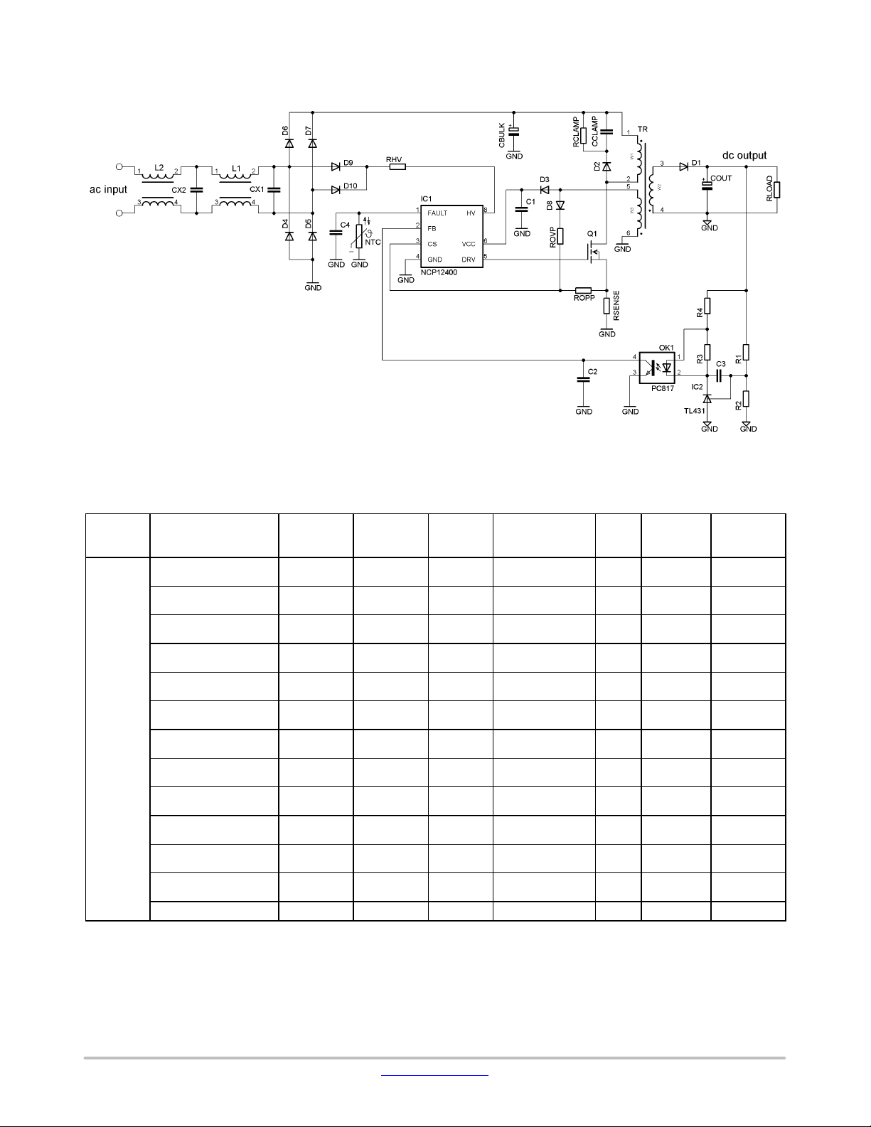
TYPICAL APPLICATION SCHEMATIC
Figure 1. Flyback Converter Application using the NCP12400
NCP12400
Start − Stop
BO
Current
Setpoint
only
800 Hz burst
800 Hz burst
only
only
only
only
only
800 Hz burst
800 Hz burst
only
800 Hz burst
Start
kHz
www.onsemi.com
2
Page 3

NCP12400
Table 2. SPECIFIC DEVICE CODE KEY
400VWXYZf
BO
OCP Fault
Frozen Current
Quiet Skip
Soft Start
Frequency
A − 229−211 V
A − Latched
A −No
A − No, min. 3
A − 10 ms
0 − 65 kHz
Table 3. PIN FUNCTION DESCRIPTION
Pin #
Pin Name
Function
Pin Description
1
FAULT
FAULT Input
Pull the pin up or down to stop the controller. An internal current source allows the
2FBFeedback + Shutdown
An optocoupler connected to ground controls the output regulation. The part goes to
3CSCurrent Sense
This input senses the primary current for current−mode operation, and offers an
4
GND
The controller ground.
5
DRV
Drive Output
Drives external MOSFET.
6
VCCVCC Input
This supply pin accepts up to 28 Vdc, with overvoltage detection. The pin is
8HVHigh−Voltage Pin
Connects to the rectified ac line to perform the functions of start−up current source,
Part
B − 111−103 V
C − 95−93 V
D − No BO
E − Brown In, no BO
Pin
B − Autorecovery
direct connection of an NTC for over temperature detection. Device can restart in
autorecovery mode or can be latched depending on the option.
the low consumption Off mode if the FB input pin is pulled to GND.
overpower compensation adjustment. This pin implements over voltage protection
as well.
connected to an external auxiliary voltage.
Setpoint
B − 150 mV
C − 170 mV
D − 190 mV
E − 210 mV
F − 230 mV
G − 250 mV
H − 300 mV
pulses
B − Yes, min. 3
pulses,
800 Hz burst
B − 4 ms
1 − 100 kHz
2 − 65 → 100 kHz
Self−Supply, brown−out detection and X2 capacitor discharge function and the HV
sensing for the overpower protection purposes.
It is not allowed to connect this pin to a dc voltage.
www.onsemi.com
3
Page 4
FAULT
FB
CS
GND
Vdd
Intc
Intc
1k
Rcla m p
1. 2 V
Vclamp
SS_end
Brown_Out
RESET
VCC
5u A
Von
Vfb(reg)
Voff
Rfb1
Internalresitance40k
Vhv DC sample
V to I
Iopc = 0 .5u*(Vhv −125)
Vdd
1uA
Vfb < 1.64 V fix current setpoint 210mV
OVP_CMP
Vov p
2. 5V
OTP_CMP
Votp
0. 4 V
Off_mode_CMP1
2.2V
Off_mode_CMP2
0. 6V
NCP12400
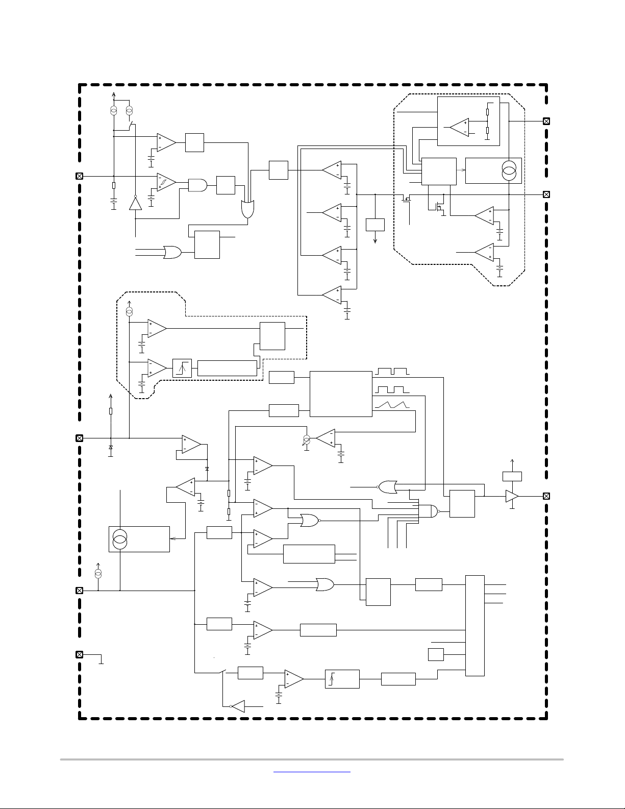
SIMPLIFIED INTERNAL BLOCK SCHEMATIC
300 us
Filter
Vfb(o pc)
Div i sion ratio 4
LEB 250 ns
LEB 120 ns
Latch
Rfb2Rf b3
OVP
OTP
Vskip
Vilim
VCSs to p
LEB 1 us
VccOVP
Set Q
Reset Qb
Skip_CMP
PWM_CMP
SoftStart_CMP
Ilimit_CMP
0.7V
CSstop_CMP
1.05V
10us
Filter
ICstart
jittering
freq folback
CSref
SkipB
Soft Start timer
VccMIN
PWM
MAX_ton
Ilimit
OVP_CMP
VccOVP_CMP
UVLO_CMP
UVLO
ON_CMP
VccON
STOP_CMP
FM input
OSC 65kHz
PFM input
Ramp_OTA
4uMho
4 events timer
26V
9.5V
12V10.5 V
Square output
ton_ max output
Saw output
1.4V
Vramp_offset
MAX_ton
Enable
SS_end
VccOVP
Vcc_Int
Vdd reg
VccOFF
Vdd
VccONVccMI N
Reset
55us
Filter
Set Q
Reset Qb
GoToOffMode timer 500ms
FBbuffer
2. 6V
Bro wn_Ou tB
QSet
Qb
4 events timer600ns timer
IC stopB
FaultB
Vhv DC sample
Brown_In
AC_Off
OM & X2 & Vcc
TSD
X2 discharge
ICstar tB
11V regulator
3. 0V
LatchB
Fault timer
control
PowerOnReset_CMP
Fault
Brown_Out
TSD
Reset
TSD
Dual HV
start−up
current source
Vcc regulator
RESET
QSet
Qb
HV
8mA
VCC
10.8V7V
Vcc( reg )VccRESET
VCC
Clamp
DRV
RESET
IC stop
Latch
Latch management
Vovp
DRV
1.05V
Figure 2. Simplified Internal Block Schematic
www.onsemi.com
4
Page 5
NCP12400
Table 4. MAXIMUM RATINGS
Rating
Symbol
Value
Unit
DRV
Maximum voltage on DRV pin
–0.3 to 20
V
V
VCCPower Supply voltage, VCC pin, continuous voltage
–0.3 to 36
VmAHV
Maximum voltage on HV pin
–0.3 to 500
V
V
Maximum voltage on low power pins (except pin 5, pin 6 and pin 8)
–0.3 to 5.5
V
R
Thermal Resistance SOIC−7
C/W
R
Thermal Resistance Junction−to−Case
73
C/W
T
Operating Junction Temperature
−40 to +150
C
T
Storage Temperature Range
−60 to +150
C
ESD Capability, HBM model (All pins except HV) (Note 1)
> 4000
V
ESD Capability, HBM model (pin 8, HV)
> 2000
V
ESD Capability, Charge Discharge Model (Note 1)
> 500
V
Table 5. ELECTRICAL CHARACTERISTICS
Characteristics
Test Condition
Symbol
Min
Typ
Max
Unit
HIGH VOLTAGE CURRENT SOURCE
Minimum voltage for current source
V
−3040
V
Current flowing out of VCC pin
VCC = 0 V
I
0.250.580.811mA
Off−state leakage current
VHV = 500 V, VCC = 15 V
I
−26
A
SUPPLY
Turn−on threshold level, VCC going up
V
11.0
12.0
13.0
V
HV current source restart threshold
V
9.5
10.5
11.5
V
Turn−off threshold
V
8.4
8.9
9.3
V
Overvoltage threshold
V
253026.5322834V
Blanking duration on V
and V
t
−10−
s
(pin 5)
(pin 6)
(pin 8)
max
q
q
JMAX
STRGMAX
(Dc−Current self−limited if operated within the allowed range) (Note 2)
CC
Power Supply voltage, VCC pin, continuous voltage (Note 2)
(Dc−Current self−limited if operated within the allowed range)
(Dc−Current self−limited if operated within the allowed range) (Note 2)
J−A
Junction-to-Air, low conductivity PCB (Note 3)
Junction-to-Air, medium conductivity PCB (Note 4)
Junction-to-Air, high conductivity PCB (Note 5)
J−C
±1000 (peak)
±30 (peak)
±20
±10 (peak)
162
147
115
mA
mA
mA
°
°
°
°
Stresses exceeding those listed in the Maximum Ratings table may damage the device. If any of these limits are exceeded, device functionality
should not be assumed, damage may occur and reliability may be affected.
1. This device series contains ESD protection and exceeds the following tests:
Human Body Model 4000 V per JEDEC standard JESD22, Method A114E
Charge Discharge Model Method 500 V per JEDEC standard JESD22, Method C101E
2. This device contains latch-up protection and exceeds 100 mA per JEDEC Standard JESD78.
3. As mounted on a 80 x 100 x 1.5 mm FR4 substrate with a single layer of 50 mm
for a JEDEC 51-1 conductivity test PCB. Test conditions were under natural convection or zero air flow.
4. As mounted on a 80 x 100 x 1.5 mm FR4 substrate with a single layer of 100 mm
for a JEDEC 51-2 conductivity test PCB. Test conditions were under natural convection or zero air flow.
5. As mounted on a 80 x 100 x 1.5 mm FR4 substrate with a single layer of 650 mm
2
of 2 oz copper traces and heat spreading area. As specified
2
of 2 oz copper traces and heat spreading area. As specified
2
of 2 oz copper traces and heat spreading area. As specified
for a JEDEC 51-3 conductivity test PCB. Test conditions were under natural convection or zero air flow.
(For typical values TJ = 25°C, for min/max values TJ = −40°C to +125°C, VHV = 125 V, VCC = 11 V unless otherwise noted)
operation
HV current source stop threshold
VCC = V
CC(on)
− 0.5 V
HV(min)
start1
I
start2
start(off)
CC(on)
15.0
16.2
(depending on the version)
CC(min)
CC(off)
Overvoltage threshold (option EAHBB,
CC(ovp)
BBBBB)
detection
CC(off)
CC(ovp)
VCC(blank)
6. Guaranteed by design.
7. CS pin source current is a sum of I
bias
and I
, thus at VHV = 125 V is observed the I
OPC
only, because I
bias
is switched off.
OPC
m
17.5
m
www.onsemi.com
5
Page 6
NCP12400
VCC decreasing level at which the internal
V
4.8
7.0
7.7
V
VCC level for I
to I
transition
V
1.0
2.1
3.0
V
Internal current consumption
DRV open, VFB = 3 V, 65 kHz
I
1.0
1.3
2.0
mA
BROWN−OUT
Brown−out thresholds (option A)
VHV going up
V
210
229
248
V
Brown−out thresholds (option B)
VHV going up
V
10294111
120
V
Brown−out thresholds (option BAHAB)
VHV going up
V
9390103
113
V
Brown−out thresholds (option C)
VHV going up
V
87859593103
V
Brown−out thresholds (option E)
VHV going up
V
90
100
110
V
Timer duration for line cycle drop−out
tHV424864738698ms
X2 DISCHARGE
Comparator hysteresis observed at HV pin
V
2.0
3.0
4.0
V
HV signal sampling period
t
−
1.0−ms
Timer duration for no line detection
t
213243
ms
Discharge timer duration
t
213243
ms
Shunt regulator voltage at VCC pin during X2
V
10.0
11.0
12.0
V
OSCILLATOR
Oscillator frequency 65 kHz version
f
619465
69
kHz
Maximum duty−ratio (corresponding to
D
758085
%
Frequency jittering amplitude, in percentage
A
3.0±4.0±5.0
kHz
Frequency jittering modulation frequency
F
85
125
165
Hz
FREQUENCY FOLDBACK
Feedback voltage threshold below which
TJ = 25°C
V
2.4
2.5
2.6
V
Feedback voltage threshold below which
TJ = 25°C
V
2.05
2.15
2.25
V
Minimum switching frequency
VFB = V
+ 0.1
f
252831
kHz
Table 5. ELECTRICAL CHARACTERISTICS
(For typical values T
SUPPLY
logic resets
= 25°C, for min/max values TJ = −40°C to +125°C, VHV = 125 V, VCC = 11 V unless otherwise noted)
J
Characteristics UnitMaxTypMinSymbolTest Condition
START1
START2
Cdrv = 1 nF, V
DRV open, VFB = 3 V, 100 kHz
Cdrv = 1 nF, VFB = 3 V, 65 kHz
= 3 V, 100 kHz
FB
Skip or before start−up
Fault mode (fault or latch)
Off−mode
VHV going down
VHV going down
VHV going down
VHV going down
CC(reset)
CC(inhibit)
CC1
I
CC2
I
CC3
I
CC4
I
CC5
HV(start)
V
HV(stop)
HV(start)
V
HV(stop)
HV(start)
V
HV(stop)
HV(start)
V
HV(stop)
HV(start)
1.1
1.5
2.0
400
300
−
194
1.4
2.1
2.6
500
430
25
211
103
100
2.1
2.9
3.4
650
550
−
228
116
110
101
mA
mA
mA
mA
mA
mA
(depending on the version)
discharge event
Oscillator frequency 100 kHz version
maximum on time at maximum switching
frequency)
of F
OSC
frequency foldback starts
frequency foldback is complete
HV(hyst)
sample
DET
DIS
CC(dis)
OSC
MAX
jitter
jitter
FB(foldS)
FB(foldE)
100
110
±
6. Guaranteed by design.
7. CS pin source current is a sum of I
bias
and I
skip(in)
, thus at VHV = 125 V is observed the I
OPC
www.onsemi.com
6
OSC(min)
only, because I
bias
is switched off.
OPC
Page 7
NCP12400
OUTPUT DRIVER
Rise time, 10 to 90% of V
VCC = V
+ 0.2 V,
t
−4070
ns
Fall time, 90 to 10% of V
VCC = V
+ 0.2 V,
t
−3060
ns
Current capability
VCC = V
+ 0.2 V,
mA
Clamping voltage (maximum gate voltage)
VCC = V
– 0.2 V, DRV high,
V
101214
V
High−state voltage drop
VCC = V
+ 0.2 V,
V
−−1
V
CURRENT SENSE
Input Pull−up Current
VCS = 0.7 V
I
−1−
A
Maximum internal current setpoint
VFB > 3.5 V
V
0.66
0.70
0.74
V
Propagation delay from V
detection to
VCS = V
t
−5070
ns
Leading Edge Blanking Duration for V
t
180
250
320
ns
Threshold for immediate fault protection
V
0.95
1.05
1.15
V
Leading Edge Blanking Duration for V
)
t
75
120
150
ns
Soft−start duration (option A)
From 1st pulse to VCS = V
t
−
10
13
ms
Frozen current setpoint (option B)
V
100
150
200
mV
Over voltage protection threshold when DRV
VCS going up
V
1.00
1.05
1.10
V
Blanking duration on OVP detection
t
0.7
1.0
1.3
s
Delay time constant before OTP confirmation
t
−
600−ns
INTERNAL SLOPE COMPENSATION
Slope of the compensation ramp
S
−−−32.5
−−mV /
FEEDBACK
Internal pull−up resistor
TJ = 25°C
R
304050
k
VFB to internal current setpoint division ratio
KFB−4−
−
Internal pull−up voltage on the FB pin
V
4.555.5
V
Offset between FB pin and internal FB
TJ = 25°C
V
−
0.8−V
SKIP CYCLE MODE
Feedback voltage thresholds for skip mode
VFB going down, TJ = 25°C
V
0.9
1.0
1.1
V
Minimum number of pulses in burst
n
3−−
Skip out delay
t
−−38
s
Table 5. ELECTRICAL CHARACTERISTICS
(For typical values T
DRV off
activation
= 25°C, for min/max values TJ = −40°C to +125°C, VHV = 125 V, VCC = 11 V unless otherwise noted)
J
Characteristics UnitMaxTypMinSymbolTest Condition
CC
CC
Ilimit
ILIM
C
C
C
DRV high, V
DRV low, V
CC(ovp)
R
= 33 kW, C
DRV
R
= 33 kW, DRV high
DRV
CC(off)
DRV
CC(off)
DRV
CC(off)
DRV
CC(min)
= 1 nF
= 1 nF
= 1 nF
DRV
DRV
load
ILIM
= 0 V
= V
CC
= 220 pF
rise
fall
I
DRV(source)
I
DRV(sink)
DRV(clamp)
DRV(drop)
bias
ILIM
delay
LEB
CS(stop)
−
−
300
500
−
−
m
(Note 6)
Soft−start duration (option B)
Frozen current setpoint (option D)
Frozen current setpoint (option E)
Frozen current setpoint (option H)
is low
(Note 6)
divider
CS(stop
ILIM
BCS
SSTART
I(freeze)
OVP(CS)
OVP,CS
OVP,del
comp(65kHz)
S
comp(100kHz)
FB(up)
FB(ref)
FB(off)
3.2
140
145
250
4.0
190
210
300
−50
4.8
240
270
350
m
ms
W
6. Guaranteed by design.
7. CS pin source current is a sum of I
skip(in)
V
skip(out)
P,skip
skip
only, because I
bias
1.05
1.15
is switched off.
OPC
1.25
m
bias
and I
VFB going up, TJ = 25°C
, thus at VHV = 125 V is observed the I
OPC
www.onsemi.com
7
Page 8
NCP12400
REMOTE CONTROL ON FB PIN
The voltage above which the part enters the
VCC > V
, VHV = 60 V
VON−
2.2−V
The voltage below which the part enters the
VCC > V
V
0.5
0.6
0.7
V
Minimum hysteresis between the VON and
VCC > V
, VHV = 60 V
V
500−−
mV
Pull−up current in off mode
VCC > V
I
−5−
A
Go To Off mode timer
VCC > V
t
400
500
600
ms
OVERLOAD PROTECTION
Fault timer duration
t
108
128
178
ms
Fault timer reset time
VCS < 0.7 V, D < 90% D
t
150
200
250
s
Autorecovery mode latch−off time duration
t
0.85
1.00
1.35
s
OVERPOWER PROTECTION
VHV to I
conversion ratio
K
−
0.54
−
A / V
Current flowing out of CS pin (Note 7)
VHV = 125 V
I
−
0
−
A
FB voltage above which I
is applied
VHV = 365 V
V
−
2.6−V
FB voltage below which is no I
applied
VHV = 365 V
V
−
1.6−V
FAULT INPUT
High threshold
V
going up
V
2.43
2.50
2.57
V
Low threshold
V
going down, TJ = 25°C
V
0.380
0.400
0.420
V
OTP resistance threshold (TJ = 25°C)
External NTC resistance is going
R
7.6
8.0
8.5
k
OTP resistance threshold (TJ = 80°C)
External NTC resistance is going
R
−
8.5
−
k
OTP resistance threshold (TJ = 110°C)
External NTC resistance is going
R
−
9.5
−
k
Current source for direct NTC connection
V
= 0.2 V
A
Current source for direct NTC connection
V
= 0.2 V, TJ = 25°C
I
475053
A
Blanking duration on high latch detection
t
355070
s
Blanking duration on low latch detection
t
−
350
−
s
Clamping voltage
I
= 0 mA
V
1.0
1.2
1.4
V
TEMPERATURE SHUTDOWN
Temperature shutdown
TJ going up
T
−
150
−°C
Temperature shutdown hysteresis
TJ going down
T
−30−°C
6. Guaranteed by design.
Table 5. ELECTRICAL CHARACTERISTICS
(For typical values T
on mode
off mode
V
OFF
OPC
= 25°C, for min/max values TJ = −40°C to +125°C, VHV = 125 V, VCC = 11 V unless otherwise noted)
J
Characteristics UnitMaxTypMinSymbolTest Condition
OPC
OPC
CC(off)
CC(off)
CC(off)
CC(off)
CC(off)
VHV = 162 V
= 325 V
V
HV
V
= 365 V
HV
MAX
OFF
HYST
OFF
GTOM
fault
fault,res
autorec
OPC
OPC(125)
I
OPC(162)
I
OPC(325)
I
OPC(365)
FB(OPCF)
FB(OPCE)
−
−
105
20
110
130
m
m
m
m
−
−
150
During normal operation
During soft−start
During normal operation
7. CS pin source current is a sum of I
bias
and I
Latch
Latch
down
down
down
Latch
Latch
Latch
I
= 1 mA
Latch
, thus at VHV = 125 V is observed the I
OPC
OVP
OTP
OTP
OTP
OTP
I
NTC
I
NTC(SSTART)
NTC
Latch(OVP)
Latch(OTP)
clamp0(Latch)
V
clamp1(Latch)
TSD
TSD(HYS)
only, because I
bias
30
60
1.8
50
100
2.4
is switched off.
OPC
W
W
W
m
70
140
m
m
m
3.0
Product parametric performance is indicated in the Electrical Characteristics for the listed test conditions, unless otherwise noted. Product
performance may not be indicated by the Electrical Characteristics if operated under different conditions.
www.onsemi.com
8
Page 9
NCP12400
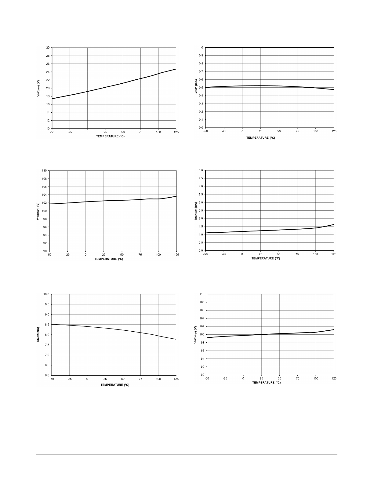
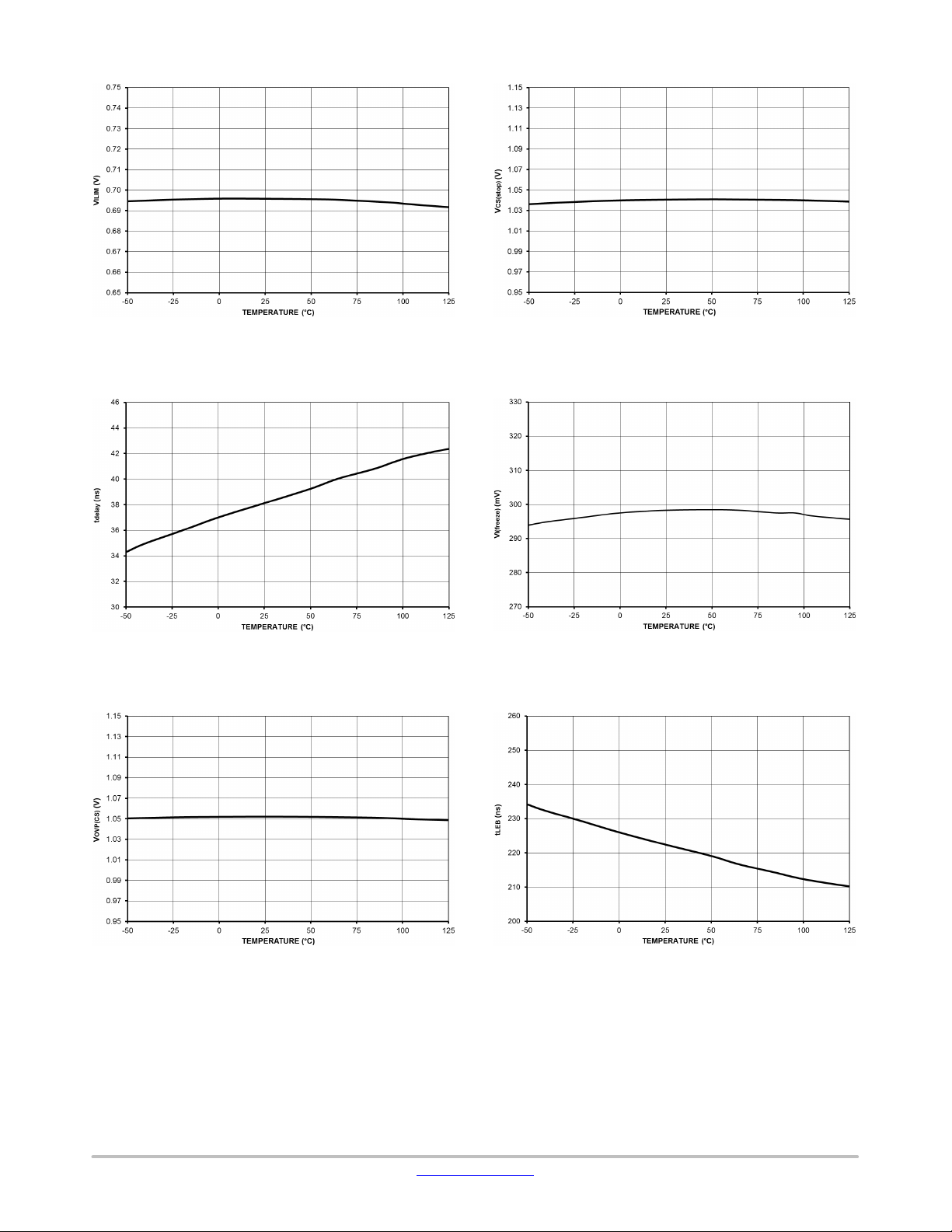
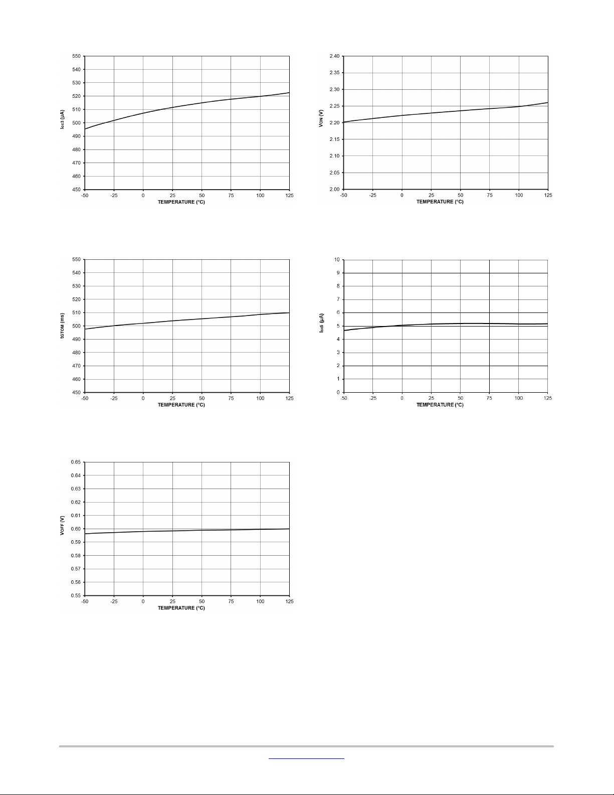
TYPICAL CHARACTERISTIC
Figure 3. Minimum Voltage for HV Current Source
Operation V
HV(min)
Figure 5. HV Pin Device Startup Threshold
V
HV(start)
Figure 4. High Voltage Startup Current Flowing
Out of V
CC
Pin I
of VCC Pin Fault/Short
start1
Figure 6. Off−state Leakage Current from HV Pin
I
start(off)
Figure 7. High Voltage Startup Current Flowing
Out of V
CC
Pin I
start2
www.onsemi.com
Figure 8. HV Pin Device Stop Threshold V
9
HV(stop)
Page 10
NCP12400
Figure 9. Maximum Internal Current Setpoint
V
ILIM
Figure 11. Propagation Delay t
delay
Figure 10. Threshold for the Very Fast Fault
Protection Activation V
Figure 12. Frozen Current Setpoint V
CS(stop)
I(freeze)
Light Load Operation
for the
Figure 13. Over Voltage Protection Threshold at
CS Pin V
OVP(CS)
www.onsemi.com
10
Figure 14. Leading Edge Blanking Duration t
LEB
Page 11
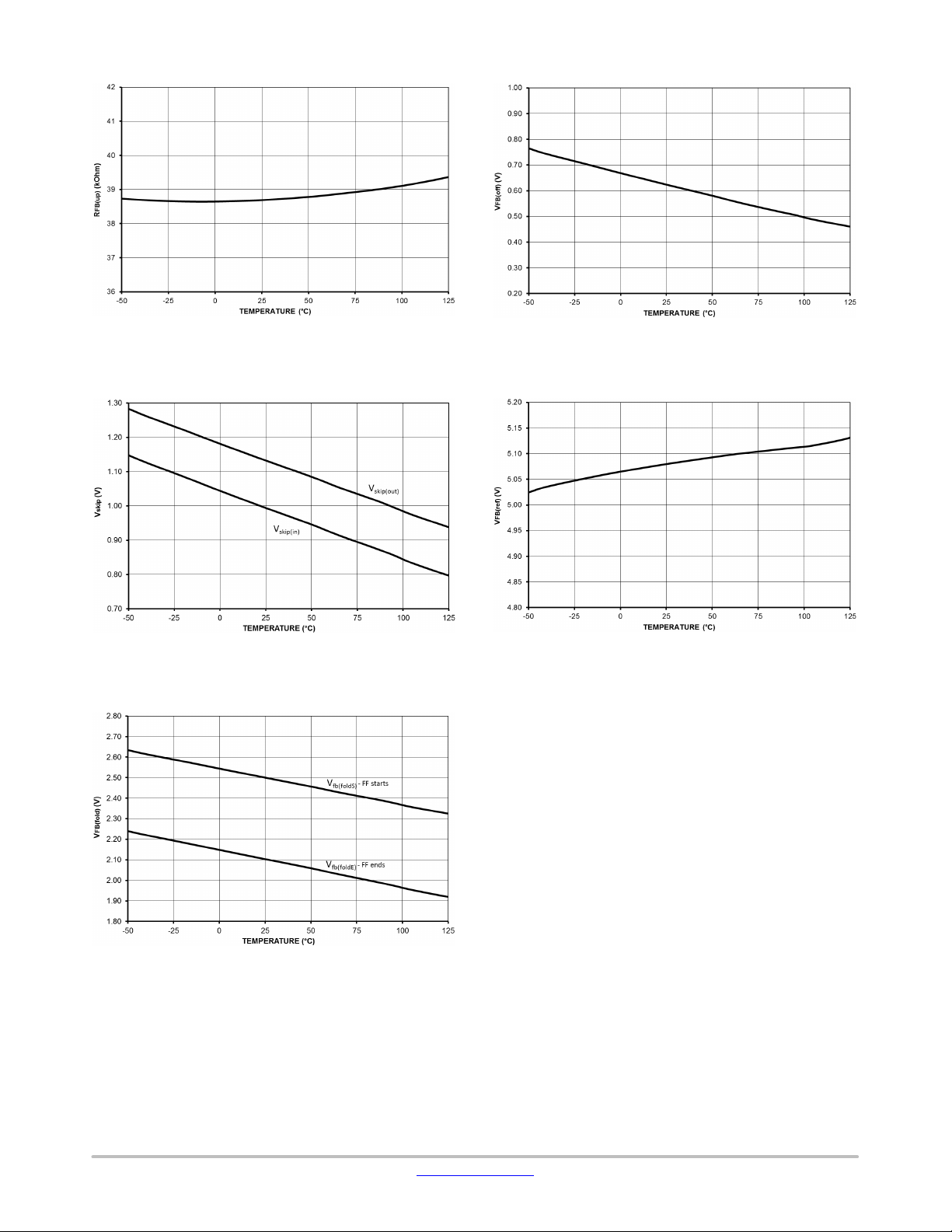
NCP12400
Figure 15. FB Pin Internal Pull−up Resistor
R
FB(up)
Figure 17. FB Pin Skip−In and Skip−Out Levels
V
skip(in)
and V
skip(out)
Figure 16. Built in Offset between FB Pin and
Internal Divider V
Figure 18. FB Pin Open Voltage V
FB(off)
FB(ref)
Figure 19. FB Pin Frequency Foldback Thresholds
V
FB(foldS)
and V
FB(foldE)
www.onsemi.com
11
Page 12
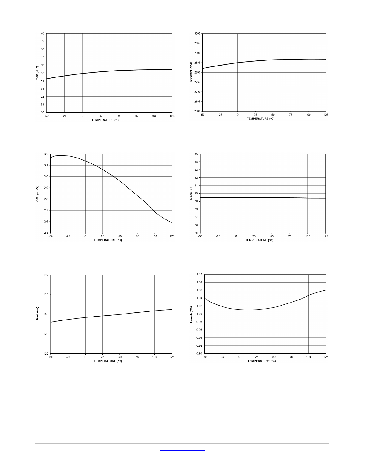
NCP12400
Figure 20. Oscillator Switching Frequency f
OSC
Figure 22. X2 Discharge Comparator Hysteresis
Observed at HV Pin V
HV(hyst)
Figure 21. Minimum Switching Frequency
f
OSC(min)
Figure 23. Maximum Duty Cycle D
MAX
Figure 24. The Fault Timer Duration t
fault
www.onsemi.com
12
Figure 25. HV Signal Sampling Period T
sample
Page 13
NCP12400
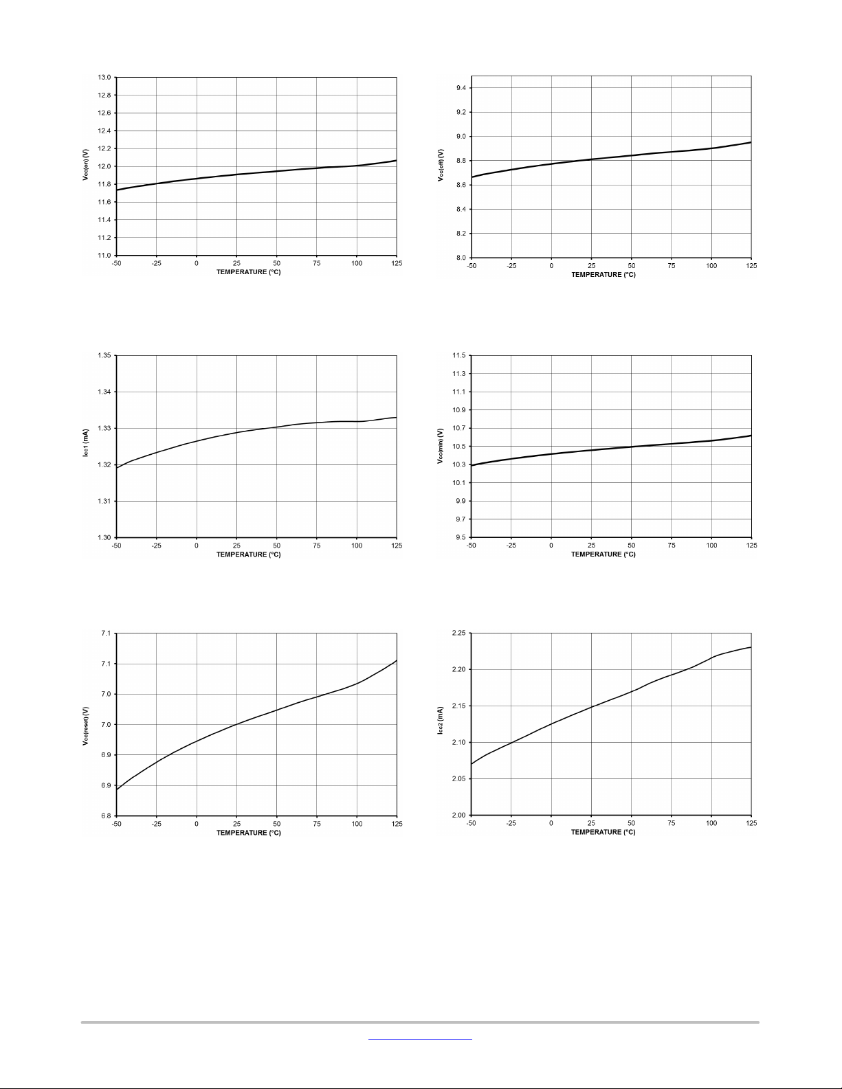
Figure 26. VCC T urn−on Threshold Level, VCC Going
Up HV Current Source Stop Threshold V
CC(on)
Figure 28. Internal Current Consumption when
DRV Pin is Unloaded I
CC1
Figure 27. VCC Turn−off Threshold (UVLO) V
CC(off)
Figure 29. HV Current Source Restart Threshold
V
CC(min)
Figure 30. VCC Decreasing Level at which the
Internal Logic Resets V
CC(reset)
Figure 31. Internal Current Consumption when
www.onsemi.com
13
DRV Pin is Loaded by 1 nF Capacitance I
CC2
Page 14
NCP12400
Figure 32. Internal Current Consumption in Skip
Mode I
CC3
Figure 34. Go To Off Mode Timer Duration t
GTOM
Figure 33. FB Pin Voltage Level Above which is
Entered Normal Operating Mode V
ON
Figure 35. Internal Current Consumption in Off
Mode I
CC5
Figure 36. FB Pin Voltage Level Below which is
Entered Off Mode V
OFF
www.onsemi.com
14
Page 15
NCP12400
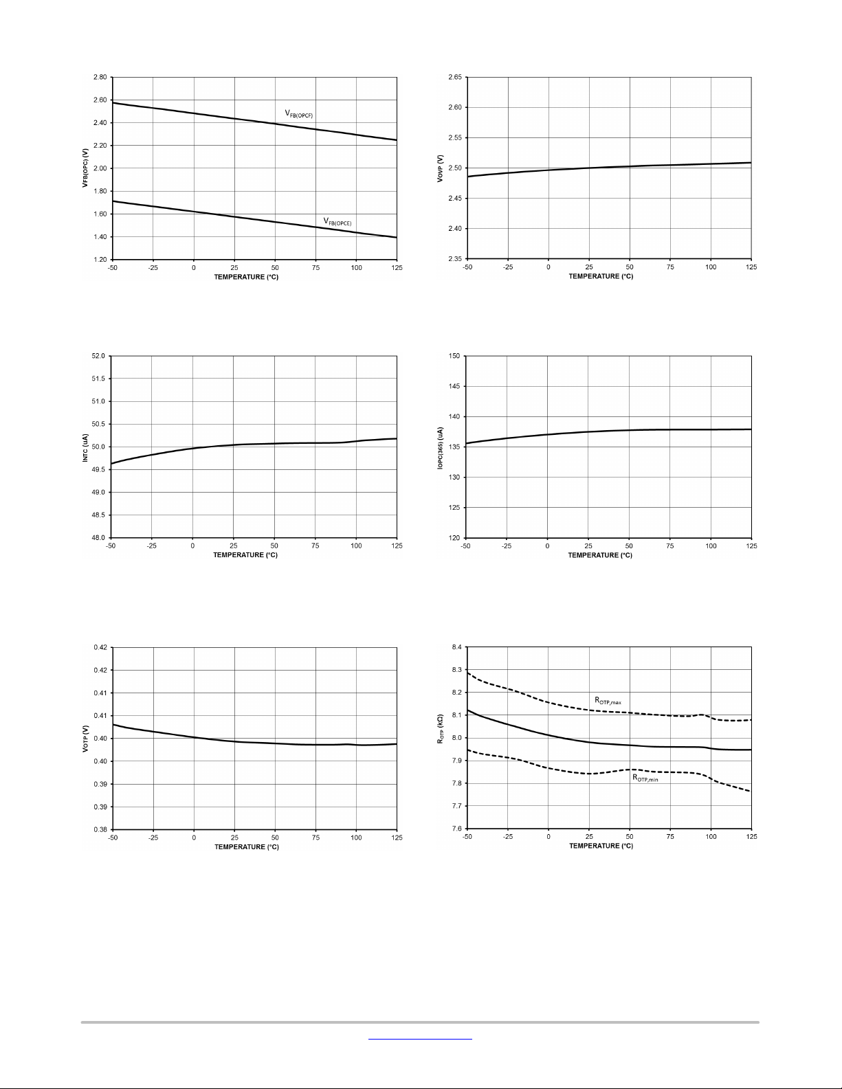
Figure 37. FB Pin Voltage Thresholds for
Overpower Compensation
Figure 39. Current I
Sourced Out from the
NTC
Fault Pin, allowing Direct NTC Connection
Figure 38. Fault Pin High Threshold for OVP V
Figure 40. Current Flowing Out from CS Pin for
Over Power Compensation @ 365 V at HV Pin
I
OPC(365)
OVP
Figure 41. Fault Pin Low Threshold for OTP V
OTP
NOTE: The OTP resistance maximum and minimum courses
are not the guaranteed limits, but the maximum and minimum
measured data values from the device characterization.
www.onsemi.com
15
Figure 42. The OTP Resistance Threshold R
OTP
Page 16

NCP12400
APPLICATION INFORMATION
Functional Description
The NCP12400 includes all necessary features to build a
safe and efficient power supply based on a fixed−frequency
flyback converter. The NCP12400 is a multimode controller
as illustrated in Figure 43. The mode of operation depends
upon line and load condition. Under all modes of operation,
the NCP12400 terminates the DRV signal based on the
switch current. Thus, the NCP12400 always operates in
current mode control so that the power MOSFET current is
always limited.
Under normal operating conditions, the FB pin commands
the operating mode of the NCP12400 at the voltage
thresholds shown in Figure 43. At normal rated operating
loads (from 100% to approximately 33% full rated power)
the NCP12400 controls the converter in a fixed−frequency
PWM mode. It can operate in the continuous conduction
mode (CCM) or discontinuous conduction mode (DCM)
depending upon the input voltage and loading conditions. If
the controller is used in CCM with a wide input voltage
range, the duty−ratio may increase up to 50%. The build−in
slope compensation prevents the appearance of
sub−harmonic oscillations in this operating area.
Low consumption off mode
For loads that are between approximately 32% and 10%
of full rated power, the converter operates in frequency
foldback mode (FFM). If the feedback pin voltage is lower
than 1.4 V the peak switch current is kept constant and the
output voltage is regulated by modulating the switching
frequency for a given and fixed input voltage V
HV
.
Effectively, operation in FFM results in the application of
constant volt−seconds to the flyback transformer each
switching cycle. Voltage regulation in FFM is achieved by
varying the switching frequency in the range from 65 kHz
to 28 kHz. For extremely light loads (below approximately
6% full rated power), the converter is controlled using bursts
of 28 kHz pulses. This mode is known as skip mode. The
FFM, keeping constant peak current and skip mode allows
design of the power supplies with increased efficiency under
the light loading conditions. Keep in mind that the
aforementioned boundaries of steady−state operation are
approximate because they are subject to converter design
parameters.
OFF
Skip mode
0 V
V
OFF
V
skip(in)
V
skip(out)
V
FB(foldE)
Figure 43. Mode Control with FB Pin Voltage
There was implemented the low consumption off mode
allowing to reach extremely low no load input power. This
mode is controlled by the FB pin and allows the remote
control (or secondary side control) of the power supply
shut−down. Most of the device internal circuitry is unbiased
in the low consumption off mode. Only the FB pin control
circuitry and X2 cap discharging circuitry is operating in the
low consumption off mode. If the voltage at feedback pin
ON
FFM
ON
V
FB(foldS)
PWM at f
OSC
FBilimV
decreases below the 0.6 V the controller will enter the low
consumption of f mode. The controller can start if the FB pin
voltage increases above the 2.2 V level.
See the detailed status diagrams for the both versions fully
latched A and the autorecovery B on the following figures.
The basic status of the device after wake–up by the V
the off mode and mode is used for the overheating protection
mode if the thermal shutdown protection is activated.
V FBV
is
CC
www.onsemi.com
16
Page 17

NCP12400
LatchCondition =
Conditions for Latched version (A)
OVP + OTP + V
Dynamic Self−Supply
CCovp
*t
VCC(blank)
+ (V
CSstop
*4clk ) + ( V
ILIM
+MaxDC )*t
fault
AutoRec
LatchCondition
AutorecoveryCondition = (V
LatchCondition = OVP + OTP + V
Conditions for Autorecovery version (B)
V
CC
<V
CCreset
AutoRec =0
Power On
Latch = 0
Reset
V
CC
<V
CCreset
(V
FB
<V
OFF
AutoRec =X
Off Mode
Latch =X
V
FB
>V
ON
AutoRec = X
Latch =X
Check
)*GTOMtimer *(V
CC
>V
CCoff
)
Latch *AutoRec
BO
AutoRec =0
Latch =1
Latch
BO
AutoRec =0
Latch =0
Reset
BO+TSD
Extra Low Consumption
V
HV
>V
HV(min)
Discharge
Latch = 0
X2 cap
No AC
CSstop
*4clk ) + ( V
ILIM
+MaxDC )*t
fault
+ (V
CC
<V
CCoff
)*t
VCC(blank )
CCovp
*t
VCC (blank )
V
CSstop
V
CC
<V
CCoff
Dynamic Self−Supply
(if not enoughgh auxiliary voltage is
AutoRec =1
fault
mode
present)
Autorecovery
Latch
V
CC
>V
CCoff
V
CC
Skip
Skip out
delay
BO
Skip in
Stop
(V
CC
>V
CCon
)*BO
Start
Soft
SSend
Running
BO+TSD
Efficient operating mode
Skip in
Figure 44. Operating Status Diagram of the Device
www.onsemi.com
17
Page 18

NCP12400
Before start
Normal mode
Overload
V
CC(inhibit)
source= I
HV current
start1
source=I
HV current
start2
V
CC(min)
CC(dis)
V
V
CC(on)
V
CC(off)
VCC
is trigged before OCP timer elapsed
t
Fault mode
Low consumption off mode
discharge
X2
autorec
time
Figure 45. VCC Management Timing Diagram
UVLO level V
CC(off)
The information about the fault (permanent Latch or
Autorecovery) is kept during the low consumption off mode
due the safety reason. The reason is not to allow unlatch the
device by the remote control being in off mode.
www.onsemi.com
Start−up of the Controller
At start−up, the current source turns on when the voltage
on the HV pin is higher than V
V
18
reaches V
CC
, then turns on again when VCC reaches
CC(on)
, and turns off when
HV(min)
Page 19

NCP12400
V
proper start−up, i.e. when V
controller actually starts the next time V
, until the input voltage is high enough to ensure a
CC(min)
reaches V
HV
reaches V
CC
HV(start)
. The
CC(on)
The controller then delivers pulses, starting with a soft−start
period t
during which the peak current linearly
SSTART
increases before the current−mode control takes over.
Even though the Dynamic Self−Supply is able to maintain
the V
voltage between V
CC
CC(on)
and V
CC(min)
by turning
the HV start−up current source on and off, it can only be used
in light load condition, otherwise the power dissipation on
VHV
V
HV(start)
the die would be too much. As a result, an auxiliary voltage
source is needed to supply V
.
The Dynamic Self−Supply is useful to keep the controller
during normal operation.
CC
alive when no switching pulses are delivered, e.g. in
brown−out condition, or to prevent the controller from
stopping during load transients when the V
The NCP12400 accepts a supply voltage as high as 28 V,
with an overvoltage threshold V
that latches the
CC(ovp)
controller off.
might drop.
CC
V
HV(min)
V
CC(on)
V
CC(min)
V
CC(inhibit)
DRV
VCC
HV current
source = I
start1
Figure 46. VCC Start−up Timing Diagram
HV current
source = I
start2
Waits next
before starting
V
CC(on)
time
time
time
For safety reasons, the start−up current is lowered when
V
is below V
CC
case the V
CC(inhibit)
pin is shorted to GND (in case of VCC capacitor
CC
failure, or external pull−down on V
, to reduce the power dissipation in
to disable the
CC
www.onsemi.com
controller). There is only one condition for which the current
source doesn’t turn on when V
voltage on HV pin is too low (below V
19
reaches V
CC
HV(min)
CC(inhibit)
).
: the
Page 20

V
HV(start)
V
V
V
HV(min)
VCC
CC(on)
CC(min)
VHV
NCP12400
Device starts at
V
event
CC(on)
time
V
CC(off)
HV current
source = I
V
CC(inhibit)
HV current
source = I
start1
DRV
Figure 47. Latch After the Preshort
HV Sensing of Rectified AC Voltage
The NCP12400 features on its HV pin a true ac line
monitoring circuitry. It includes a minimum start−up
threshold and an autorecovery brown−out protection; both
of them independent of the ripple on the input voltage. It is
allowed only to work with an unfiltered, rectified ac input to
ensure the X2 capacitor discharge function as well, which is
described in following. The brown−out protection
start2
UVLO level V
is trigged before OCP timer elapsed
Device stops thanks
to pre−short protection
CC(off )
time
time
thresholds are fixed, but they are designed to fit most of the
standard ac−dc conversion applications.
When the input voltage goes below V
HV(stop)
brown−out condition is detected, and the controller stops.
The HV current source maintains V
V
V
levels until the input voltage is back above
CC(min)
HV(start)
.
between V
CC
CC(on)
, a
and
www.onsemi.com
20
Page 21

NCP12400
V
HV(start )
V
HV(stop)
HV stop
V
CC(on)
V
CC(min)
VHV
VCC
HV timer elapsed
time
Brown−out
t
HV
detected
Waits next
VccON before
starting
time
DRV
Figure 48. Ac Line Drop−out Timing Diagram
When VHV crosses the V
HV(start)
can start immediately. When it crosses V
a timer of duration t
, this ensures that the controller
HV
threshold, the controller
HV(stop)
, it triggers
doesn’t stop in case of line cycle drop−out.
When V
starts when the V
it crosses V
crosses the V
HV
CC
HV(stop)
HV(start)
crosses the next V
threshold, the controller
event. When
CC(on)
, it triggers a timer of duration tHV, this
ensures that the controller doesn’t stop in case of line cycle
Brown−out
condition
resets the
Internal Latch
time
time
drop−out. The device restart after the ac line voltage
drop−out is protected to the parasitic restart initiated e.g. the
spikes induced at HV pin immediately after the device is
stopped by the residual energy in the EMI filter. The device
restart is allowed only after the 1
st
watch dog signal event.
The basic principle is shown at Figure 49 and detail of the
device restart is shown at Figure 50.
www.onsemi.com
21
Page 22

NCP12400
V
HV(start)
V
HV(stop)
HV stop
V
CC(on)
VHV
V
CC
HV timer elapsed
Spike induced by
residual energy in
EMI filter
Brown−out
t
HV
detected
Waits next
VccON before
starting
time
time
V
CC(min)
DRV
Brown−out
condition
resets the
Internal Latch
Figure 49. Ac Line Drop−out Timing Diagram with the Parasitic Spike
time
time
www.onsemi.com
22
Page 23

NCP12400
VHV
SAMPLE
V
HV( start )
V
HV( stop )
V
HV (hyst )
Comparator
Output
Sample clock
T
SAMPLE
1stHV edge
resets the watch
dog and starts
the peak
detection of HV
pin signal
time
time
Watch dog
signal
HV stop
VCC
V
CC(on )
V
CC(mini)
DRV
2ndsample clock
pulse after last
HV edge initiates
the watch dog
signal
t
HV
Brown−out
detected
Device is stopped
Device restarts
2ndsample clock
pulse after last
HV edge initiates
the watch dog
signal
Device can restart after
st
1
Watch dog signal
when HV signal
crosses V
HV(start )
level
time
time
time
time
Figure 50. Detailed Timing Diagram of the Device Restart after the Short ac Line Drop−out
www.onsemi.com
23
time
Page 24

NCP12400
X2 Cap Discharge Feature
The X2 capacitor discharging feature is offered by usage
of the NCP12400. This feature save approx. 16 mW –
25 mW input power depending on the EMI filter X2
capacitors volume and it saves the external components
count as well. The discharge feature is ensured via the
start−up current source with a dedicated control circuitry for
this function. The X2 capacitors are being discharged by
current defined as I
when this need is detected.
start2
There is used a dedicated structure called ac line unplug
detector inside the X2 capacitor discharge control circuitry.
See the Figure 51 for the block diagram for this structure and
Figures 52, 53, 54 and 55 for the timing diagrams. The basic
idea of ac line unplug detector lies in comparison of the
direct sample of the high voltage obtained via the high
voltage sensing structure with the delayed sample of the high
voltage. The delayed signal is created by the sample & hold
structure.
The comparator used for the comparison of these signals
is without hysteresis inside. The resolution between the
slopes of the ac signal and dc signal is defined by the
sampling time T
SAMPLE
and additional internal offset NOS.
These parameters ensure the noise immunity as well. The
additional offset is added to the picture of the sampled HV
signal and its analog sum is stored in the C
storage
1
capacitor. If the voltage level of the HV sensing structure
output crosses this level the comparator CMP output signal
resets the detection timer and no dc signal is detected. The
additional offset N
can be measured as the V
OS
HV(hyst)
on
the HV pin. If the comparator output produces pulses it
means that the slope of input signal is higher than set
resolution level and the slope is positive. If the comparator
output produces the low level it means that the slope of input
signal is lower than set resolution level or the slope is
negative. There is used the detection timer which is reset by
any edge of the comparator output. It means if no edge
comes before the timer elapses there is present only dc signal
or signal with the small ac ripple at the HV pin. This type of
the ac detector detects only the positive slope, which fulfils
the requirements for the ac line presence detection.
In case of the dc signal presence on the high voltage input,
the direct sample of the high voltage obtained via the high
voltage sensing structure and the delayed sample of the high
voltage are equivalent and the comparator produces the low
level signal during the presence of this signal. No edges are
present at the output of the comparator, that’s why the
detection timer is not reset and dc detect signal appears.
The minimum detectable slope by this ac detector is given
by the ration between the maximum hysteresis observed at
HV pin V
HV(hyst),max
and the sampling time:
V
+
HV(hyst),max
T
sample
S
min
(eq. 1)
Than it can be derived the relationship between the
minimum detectable slope and the amplitude and frequency
of the sinusoidal input voltage:
V
V
max
HV(hyst),max
+
2 @ p @ f@ T
+ 22.7 V
sample
+
2 @ p @ 35@ 1@ 10
5
−3
+
(eq. 2)
The minimum detectable AC RMS voltage is 16 V at
frequency 35 Hz, if the maximum hysteresis is 5 V and
sampling time is 1 ms.
The X2 capacitor discharge feature is available in any
controller operation mode to ensure this safety feature. The
detection timer is reused for the time limiting of the
discharge phase, to protect the device against overheating.
The discharging process is cyclic and continues until the ac
line is detected again or the voltage across the X2 capacitor
is lower than V
. This feature ensures to discharge
HV(min)
quite big X2 capacitors used in the input line filter to the safe
level. It is important to note that it is not allowed to
connect HV pin to any dc voltage due this feature. e.g.
directly to bulk capacitor.
During the HV sensing or X2 cap discharging the V
is kept above the V
voltage by the Self−Supply in any
CC(off)
CC
net
mode of device operation to supply the control circuitry.
During the discharge sequence is not allowed to start−up the
device.
www.onsemi.com
24
Page 25

NCP12400
Figure 51. The ac Line Unplug Detector Structure Used for X2 Capacitor Discharge System
Figure 52. The ac Line Unplug Detector Timing Diagram
www.onsemi.com
25
Page 26

NCP12400
Figure 53. The ac Line Unplug Detector Timing Diagram Detail with Noise Effects
www.onsemi.com
26
Page 27

VHV
NCP12400
V
HV(start)
V
HV(stop)
Starts
only at
V
CC(on)
One Shot
DRV
X2 discharge
current
HV
timer
starts
HV
timer
restarts
AC line unplug
X2 capacitor
discharge
time
AC line Unplug
detector starts
No AC detection
t
HV
t
DET
time
Brown−out
X2 discharge
time
t
DIS
V
CC
V
CC(on)
V
CC(dis)
V
CC(min)
Figure 54. HV Pin ac Input Timing Diagram with X2 Capacitor Discharge Sequence when the Application is
Unplugged Under Extremely Low Line Condition
time
time
www.onsemi.com
27
Page 28

NCP12400
VHV
V
HV(start)
V
HV(stop)
Starts
only at
V
CC(on)
One Shot
DRV
X2 discharge
current
HV
timer
starts
HV
timer
restarts
AC line unplug
AC line Unplug
detector starts
t
DET
X2 capacitor
discharge
No AC detection
X2 discharge
t
DIS
X2 capacitor
discharge
t
HV
time
t
DET
time
Device is stopped
X2 discharge
t
DIS
time
V
CC
V
CC(dis)
Device shunts the
X2 discharge
current internally
Figure 55. HV Pin ac Input Timing Diagram with X2 Capacitor Discharge Sequence When the Application is
Unplugged Under High Line Condition
The Low Consumption Off Mode
There was implemented the low consumption off mode
allowing to reach extremely low no load input power as
described in previous chapters. If the voltage at feedback pin
decreases below the 0.6 V the controller enters the off mode.
The internal V
low V
CC
is turned−off, the IC consumes extremely
CC
current and only the voltage at external V
CC
capacitor is maintained by the Dynamic Self−Supply circuit.
The Dynamic Self−Supply circuit keeps the V
between the V
CC(on)
and V
levels. The supply for the
CC(off)
voltage
CC
FB pin watch dog circuitry and FB pin bias is provided via
the low consumption current sources from the external V
CC
capacitor. The controller can only start, if the FB pin voltage
increases above the 2.2 V level. See Figure 56 for timing
Only the X2 cap discharge and Self−Supply features is
enabled in the low consumption off mode. The X2 cap
discharging feature is enable due the safety reasons and the
Self−Supply is enabled to keep the V
very low V
consumption appears in this mode. Any other
CC
supply, but only
CC
features are disabled in this mode.
The information about the latch status of the device is kept
in the low consumption off mode and this mode is used for
the TSD protection as well. The protection timer
GoToOffMode t
is used to protect the application
GTOM
against the false activation of the low consumption off mode
by the fast drop outs of the FB pin voltage below the 0.4 V
level. E.g. in case when is present high FB pin voltage ripple
during the skip mode.
diagrams.
time
time
www.onsemi.com
28
Page 29

NCP12400
e
f
f
f
VHV
V
HV(start)
VFB
V
ON
V
OFF
VCC
V
CC(on)
V
CC(dis)
V
CC(off)
V
CC(inhibit)
One Shot
DRV start
condition
Low consumption mode
DSS start to
charge the Vcc
cap
HV
timer
starts
Ready to RUN
Starts
only at
V
CC(on)
RUN
HV
timer
restarts
Low consumption off mode
t
GTSG
Self−Supply
in off mode
AC line unplug
Dynamic
AC line Unplug
detector starts
X2 capacitor
discharge
No AC detection
X2 capacitor
discharge
time
No AC detection
time
DRV
current
X2 discharge
Figure 56. Start−up, Shut−down and AC Line Unplug Time Diagram
Oscillator with Frequency Jittering
The NCP12400 includes an oscillator that sets the
switching frequency 65 kHz or 100 kHz depending on the
version. The maximum duty−ratio of the DRV pin is 80%.
In order to improve the EMI signature, the switching
frequency jitters ±4 kHz around its nominal value, with a
triangle−wave shape and at a frequency of 125 Hz. This
frequency jittering is active even when the frequency is
decreased to improve the efficiency in light load condition.
Skip mode
+ 4 kHz
OSC
Nominal f
− 4 kHz
OSC
OSC
OSC
t
DET
t
DET
time
X2 cyclic discharge
process starts
time
t
DIS
t
DIS
time
8 ms
Tim
(125 Hz)
Figure 57. Frequency Modulation of the Maximum
Switching Frequency
www.onsemi.com
29
Page 30

NCP12400
Low Load Operation Modes: Frequency Foldback
Mode (FFM) and Skip Mode
In order to improve the efficiency in light load conditions,
the frequency of the internal oscillator is linearly reduced
from its nominal value down to f
OSC(min)
. This frequency
foldback starts when the voltage on FB pin goes below
Vfb(foldS), and is complete when Vfb reaches Vfb(foldE).
The maximum on−time duration control is kept during the
f
OSC
f
OSC(min)
Fsw
Skip
V
skip(in) V
V
skip(out)
Figure 58. Frequency Foldback Mode Characteristic
V
FB(foldE)
Fixed I
peak
V
FB(freeze)
frequency foldback mode to provide the natural transformer
core anti−saturation protection. The frequency jittering is
still active while the oscillator frequency decreases as well.
The current setpoint is fixed to 300 mV in the frequency
foldback mode if the feedback voltage decreases below the
Vfb(freeze) level. This feature increases efficiency under
the light loads conditions as well.
FB
FB(foldS)
V
offset+KFB
V
X
ILIM
Internal current setpoint
V
V
I(freeze)
ILIM
V
skip(in) V
V
skip(out)
Fixed I
V
FB(foldE)
peak
V
Figure 59. Current Setpoint Dependency on the Feedback Pin Voltage
When the FB voltage reaches V
while decreasing,
skip(in)
skip mode is activated: the driver stops, and the internal
consumption of the controller is decreased. While V
below V
soon as V
, the controller remains in this state; but as
skip(out)
crosses the skip out threshold, the DRV pin
FB
FB
is
starts to pulse again.
FB(freeze)
V
FB
K
V
X
FB
FB(foldS)
ILIM
The NCP12400 device includes logic which allows going
into skip mode after the DRV cycle is finished by reaching
of the peak current value. This technique eliminates the last
short pulses in skip mode, which increases the system
efficiency at light loads and makes easier the application of
active secondary rectification circuitry.
www.onsemi.com
30
Page 31

FB
NCP12400
Figure 60. Skip Mode Timing Diagram
V
skip(out)
V
skip(in)
OSC
(internal signal)
CS
V
I(freeze)
Skip signal does
not immediately
stop the pulse
Enters
skip
Figure 61. Technique Preventing Short Pulses in Skip Mode
time
time
time
www.onsemi.com
31
Page 32

NCP12400
Quiet−Skip
To further avoid acoustic noise, the circuit prevents the
burst frequency during skip mode from entering the audible
range by limiting it to a maximum of 800 Hz. This is
achieved via a timer t
that is activated during
quiet
Quiet−Skip. The start of the next burst cycle is prevented
until this timer has expired. As the output power decreases,
the switching frequency decreases. Once it hits minimum
switching frequency f
OSC(min)
, the skip−in threshold is
reached and burst mode is entered − switching stops as soon
as the current drive pulses ends – it does not stop
immediately.
Once switching stops, FB will rise. As soon as FB crosses
the skip−exit threshold, drive pulses will resume, but the
controller remains in burst mode. At this point, a 1250 ms
(typ) timer t
pulses counter. This n
is started together with a count to n
quiet
pulses counter ensures the
P,sk ip
P,sk ip
minimum number of DRV signal pulses in burst. The next
time the FB voltage drops below the skip−in threshold, DRV
pulses stop at the end of the current pulse as long as n
P,sk ip
drive pulses have been counted (if not, they do not stop until
the end of the n
−th pulse). They are not allowed to start
P,sk ip
again until the timer expires, even if the skip−exit threshold
is reached first. It is important to note that the timer will not
force the next cycle to begin – i.e. if the natural skip
frequency is such that skip−exit is reached after the timer
expires, the drive pulses will wait for the skip−exit
threshold.
This means that during no−load, there will be a minimum
of n
drive pulses, and the burst−cycle period will likely
P,sk ip
be much longer than 1250 ms. This operation helps to
improve efficiency at no−load conditions.
In order to exit burst mode, the FB voltage must rise higher
than V
skip(tran)
level. If this occurs before t
expires, the
quiet
drive pulses will resume immediately – i.e. the controller
won’t wait for the timer to expire. Figure 63 provides an
example of how Quiet−Skip works, while Figure 62 shows
the immediate leaving the quiet skip mode by crossing the
transient enhancement level V
skip(tran)
.
www.onsemi.com
32
Page 33

V
skip(tran)
V
skip(out)
V
skip(in)
NCP12400
V
FB
Crossing the transient
enhancement level
stops the quiet skip
immediately
Exits skip
after quiet
timer
expires
Time
V
V
V
DRV
V
skip(out)
skip(in)
DRV
V
skip(out)
V
skip(in)
quiet
t
t
quiet
Enters
skip
Enters
skip
Time
Figure 62. Leaving the Quiet−Skip Mode during Load Transient
FB
Running just above skip
mode with f
Sequence of events
1; 2; 3 starts the quiet
FB
2
1
3
skip mode
sw=fosc(min)
The DRV pulses does not
start even when V
in the quiet skip mode
FB>Vskip(out)
time
time
V
skip(tran)
V
skip(out)
V
DRV
V
FB
skip(in)
DRV
n
P,skip
n
P,skip
forces at least n
pulses in skip mode
t
quiet
n
P,skip
t
quiet
DRV pulses does
not start because
V
FB<Vskip(in)
Quiet skip mode
burst
p,skip
n
P,skip
Figure 63. Quiet−Skip Timing Diagram − option
When VFB>V
skip (tran )
mode immediately finishes
t
quiet
the quiet skip
t
quiet
n
P,skip
time
time
time
time
www.onsemi.com
33
Page 34

NCP12400
Clamped Driver
The supply voltage for the NCP12400 can be as high as
36 V , but most of the MOSFET s that will be connected to the
DRV pin cannot accept more than 20 V on their gate. The
driver pin is therefore safely clamped below 16 V. This
driver has a typical capability of 500 mA for source current
and 800 mA for sink current.
Current−Mode Control With Slope Compensation and
Soft−Start
NCP12400 is a current−mode controller, which means
that the FB voltage sets the peak current flowing in the
transformer primary inductance and the MOSFET. This is
done through a PWM comparator: the current is sensed
across a res i s t o r and the resulting voltage is applied to the CS
pin. It is applied to one input of the PWM comparator
through a 250 ns LEB block. On the other input the FB
VFB
KFBx V
ILIM
voltage subducted by offset typically 0.8 V and divided by
4 sets the threshold: when the voltage ramp reaches this
threshold, the output driver is turned off. The maximum
value for the current sense is 0.7 V, and it is set by a dedicated
comparator.
Each time the controller is starting, i.e. the controller was
off and starts – or restarts – when V
reaches V
CC
CC(on)
, a
soft−start is applied: the current sense set−point is increased
by 32 discrete steps from 0 (the minimum level can be higher
than 0 because of the LEB and propagation delay) until it
reaches V
(after a duration of t
ILIM
), or until the FB
SSTART
loop imposes a setpoint lower than the one imposed by the
soft−start (the 2 comparators outputs are OR’ed).
During the soft−start the oscillator frequency increase
from the minimum switching frequency to the maximum
switching frequency following the ramp applied to current
sense set−point.
Soft−start ramp
V
ILIM
CS Setpoint
V
ILIM
VFB takes
over soft −start
Time
Soft−start ramp
V
ILIM
t
SSTART
Time
OSC frequency
f
SW
f
SW,min
Figure 64. Soft−Start Feature
t
SSTART
t
SSTART
TimeTime
Time
www.onsemi.com
34
Page 35

NCP12400
Under some conditions, like a winding short−circuit for
instance, not all the energy stored during the on−time is
transferred to the output during the off−time, even if the
on−time duration is at its minimum (imposed by the
propagation delay of the detector added to the LEB
duration). As a result, the current sense voltage keeps on
increasing above V
, because the controller is blind
ILIM
during the LEB blanking time. Dangerously high current
can grow in the system if nothing is done to stop the
controller. That’s what the additional comparator, that
senses when the current sense voltage on CS pin reaches
V
CS(stop)
( = 1.5 x V
), does: as soon as this comparator
ILIM
toggles, the controller immediately enters the protection
mode.
In order to allow the NCP12400 to operate in CCM with
a duty−ratio above 50%, the fixed slope compensation is
internally applied to the current−mode control. The slope
appearing on the internal voltage setpoint for the PWM
comparator is −32.5 mV/ms typical. The slope compensation
can be observable as a value of the peak current at CS pin.
The internal slope compensation circuitry uses a saw−tooth
signal synchronized with the internal oscillator is subtracted
from the FB voltage divided by K
FB
.
Internal PWM setpoint
/ K
V
FB
V
/ KFB − 0.2 V
FB
Figure 65. Slope Compensation Block Diagram
FB
40% 100%80%0%
Figure 66. Slope Compensation Timing Diagram
www.onsemi.com
35
Duty Cycle
Page 36

NCP12400
Internal Overpower Protection
The power delivered by a flyback power supply is
proportional to the square of the peak current in
discontinuous conduction mode:
P
OUT
1
+
@ h @ LP@ FSW@ I
2
I
peak
I
LIMIT
Figure 67. Needs for Line Compensation For True Overpower Protection
P
High
Line
2
t
delay
(eq. 3)
To compensate this and have an accurate overpower
protection, an offset proportional to the input voltage is
added on the CS signal by turning on an internal current
source: by adding an external resistor in series between the
sense resistor and the CS pin, a voltage offset is created
across it by the current. The compensation can be adjusted
by changing the value of the resistor.
I
OPC
Unfortunately, due to the inherent propagation delay of
the logic, the actual peak current is higher at high input
voltage than at low input voltage, leading to a significant
difference in the maximum output power delivered by the
power supply.
DI
to be
peak
compensated
Low
Line
time
t
delay
But this offset is unwanted to appear when the current
sense signal is small, i.e. in light load conditions, where it
would be in the same order of magnitude. Therefore the
compensation current is only added when the FB voltage is
higher than V
FB(OPCE)
. However, because the HV pin is
being connected to ac voltage, there is needed an additional
circuitry to read or at least closely estimate the actual voltage
on the bulk capacitor.
V
HV
V
V
FB(OPCE) V
FB(OPCF)
FB
Figure 68. Overpower Protection Current Relation to Feedback Voltage
I
OPC
I
OPC(365)
I
OPC(125)
125 V
365 V
V
HV
Figure 69. Overpower Protection Current Relation to Peak of Rectified Input Line AC voltage
www.onsemi.com
36
Page 37

NCP12400
Figure 70. Block Schematic of Overpower Protection Circuit
A 5−bit A/D converter with the peak detector senses the
ac input, and its output is periodically sampled and reset, in
order to follow closely the input voltage variations. The
sample and reset events are given by the output from the ac
line unplug detector. The sensed HV pin voltage peak value
is validated when no HV edges from comparator are present
after last falling edge during 2 sample clocks. See Figure 71
for details.
Overcurrent Protection with Fault Timer
The overload protection depends only on the current
sensing signal, making it able to work with any transformer,
even with very poor coupling or high leakage inductance.
When an overcurrent occurs on the output of the power
supply, the FB loop asks for more power than the controller
www.onsemi.com
can deliver, and the CS set−point reaches V
event occurs, an internal t
timer is started: once the timer
fault
. When this
ILIM
times out , D RV pulses are stopped and the controller is either
latched of f . This latch is released in autorecovery mode. The
controller tries to restart after t
. The other possibilities
autorec
of the latch release are the brown−out condition or the VCC
power on reset. The timer is reset when the CS set−point
goes back below VILIM before the timer elapses. The fault
timer is also started if the driver signal is reset by the
maximum on time. The controller also enters the same
protection mode if the voltage on the CS pin reaches 1.5
times the maximum internal set−point V
CS(stop)
(allows to
detect winding short−circuits) or there appears low V
supply. See Figure 71 for the timing diagram.
37
CC
Page 38

NCP12400
Figure 71. Overpower Compensation Timing Diagram
www.onsemi.com
38
Page 39

NCP12400
Table 6. PROTECTION MODES AND THE LATCH MODE RELEASES
Event
Timer Protection
Next Device Status
Release to Normal Operation Mode
Overcurrent
Fault timer
Latch
Autorecovery
Maximum on time
Fault timer
Latch
Brown−out
Maximum duty cycle
Fault timer
Latch
Brown−out
Winding short
4 consecutive pulses
Latch
Autorecovery
Low supply
10 ms timer
Latch
Autorecovery
External OTP, OVP
55 ms
Latch
Brown−out
High supply
10 ms timer
Latch
Brown−out
Brown−out
HV timer
Device stops
(VHV > V
) & (VCC > V
)
Internal TSD
10 ms timer
Device stops, HV start−up
(VHV > V
) & (VCC > V
) & TSDb
Off mode
500 ms timer
Device stops and internal
(VHV > V
) & (VCC > V
) &
VCS > V
VCS > V
VCC < V
VCC > V
VHV < V
VFB < V
ILIM
CS(stop)
CC(off)
CC(ovp)
HV(stop)
OFF
current source stops
VCC is turned off
V
VCC < V
VCC < V
VCC < V
VCC < V
VCC < V
VCC < V
HV(start)
HV(start)
HV(start)
Brown−out
< V
CC
CC(reset)
CC(reset)
CC(reset)
Brown−out
CC(reset)
Brown−out
CC(reset)
CC(reset)
CC(reset)
(VFB > VON)
CC(on)
CC(on)
CC(on)
www.onsemi.com
39
Page 40

V
CC(on)
V
CC(min)
NCP12400
Figure 72. Latched Timer−Based Overcurrent Protection
www.onsemi.com
40
Page 41

NCP12400
Output Load
Max Load
Fault Flag
VCC
V
CC(on )
V
CC(min)
DRV
Overcurrent
applied
Fault
timer
starts
Restart
At V
CC
ON
(new burst
cycle if Fault
still present)
Fault
disappears
time
time
time
Fault timer
t
fault
Controller
stops
t
fault
t
autorec
Figure 73. Timer−based Protection Mode with Autorecovery Release from Latch−off
time
time
www.onsemi.com
41
Page 42

FAULT Input
NCP12400
Figure 74. OVP/OTP Detection Schematic
The FAULT input pin is dedicated to the latch−off
function: it includes 2 levels of detection that define a
working window, between a high latch and a low latch:
within these 2 thresholds, the controller is allowed to run, but
as soon as either the low or the high threshold is crossed, the
controller is latched off. The controller can be released from
the latch mode by the autorecovery, but it depends on the
version of the product. The lower threshold is intended to be
used with an NTC thermistor, thanks to an internal current
source I
NTC
.
An active clamp prevents the voltage from reaching the
high threshold if it is only pulled up by the I
current. T o
NTC
reach the high threshold, the pull−up current has to be higher
than the pull−down capability of the clamp (typically
1.5 mA at V
OVP
).
To avoid any false triggering, spikes shorter than 50 ms
(for the high latch and 65 kHz version) or 350 ms (for the low
latch) are blanked and only longer signals can actually latch
the controller.
@ I
NTC(SSTART) min
V
OTP max
C
FAULT max
t
SSTART min
+
Reset occurs when a brown−out condition is detected or
the V
is cycled down to a reset voltage, which in a real
CC
application can only happen if the power supply is
unplugged from the ac line.
Upon startup, the internal references take some time
before being at their nominal values; so one of the
comparators could toggle even if it should not. Therefore the
internal logic does not take the latch signal into account
before the controller is ready to start: once V
V
, the latch pin High latch state is taken into account
CC(on)
reaches
CC
and the DRV switching starts only if it is allowed; whereas
the Low latch (typically sensing an over temperature) is
taken into account only after the soft−start is finished. In
addition, the NTC current is doubled to I
NTC(SSTART)
during
the soft−start period, to speed up the charging of the FAULT
pin capacitor The maximum value of FAULT pin capacitor
is given by the following formula (The standard start−up
condition is considered and the NTC current is neglected):
3.2@ 10
+
−3
@ 60 @ 10
0.420
−6
F + 457 nF
(eq. 4)
www.onsemi.com
42
Page 43

V
CC(on)
V
CC(min)
NCP12400
Figure 75. Latch Timing Diagram
Temperature Shutdown
The NCP12400 includes a temperature shutdown
protection with a trip point typically at 150°C and the typical
hysteresis of 30°C. When the temperature rises above the
high threshold, the controller stops switching
instantaneously, and goes to the off mode with extremely
low power consumption. There is kept the V
supply to
CC
keep the TSD information. When the temperature falls
below the l o w t h r e shold, the start−up of the device is enabled
again, and a regular start−up sequence takes place. See the
status diagrams at the Figure 44.
www.onsemi.com
43
Page 44

NCP12400
ORDERING INFORMATION
Ordering Part No.
Overload Protection
Switching Frequency
Package
Shipping
†
NCP12400BAHAB0DR2G
Latched
65 kHz
NCP12400BAHBB0DR2G
Latched
65 kHz
NCP12400BBBBB2DR2G
Autorecovery
65 → 100 kHz
NCP12400BBHAA1DR2G
Autorecovery
100 kHz
NCP12400CAHAB0DR2G
Latched
65 kHz
NCP12400CBAAB0DR2G
Autorecovery
65 kHz
NCP12400CBBAB0DR2G
Autorecovery
65 kHz
NCP12400CBHAA0DR2G
Autorecovery
65 kHz
NCP12400EAHBB0DR2G
Latched
65 kHz
NCP12400BBBBA0DR2G
Autorecovery
65 kHz
NCP12400BBHAB0DR2
Autorecovery
65 kHz
NCP12400BBEBA0DR2G
Autorecovery
65 kHz
NCP12400BBAAA0DR2G
Autorecovery
65 kHz
SOIC−7
(Pb−Free)
†For information on tape and reel specifications, including part orientation and tape sizes, please refer to our Tape and Reel Packaging
Specifications Brochure, BRD8011/D.
2500 / Tape & Reel
www.onsemi.com
44
Page 45

MECHANICAL CASE OUTLINE
PACKAGE DIMENSIONS
SCALE 1:1
SOIC−7
CASE 751U−01
ISSUE E
DATE 20 OCT 2009
−A−
58
S
1
4
−B−
0.25 (0.010)
M
B
G
−T−
C
SEATING
PLANE
H
D
7 PL
0.25 (0.010) T
M
SAS
B
R
X 45
_
M
SOLDERING FOOTPRINT*
1.52
0.060
7.0
0.275
0.6
0.024
*For additional information on our Pb−Free strategy and soldering
details, please download the ON Semiconductor Soldering and
Mounting Techniques Reference Manual, SOLDERRM/D.
4.0
0.155
1.270
0.050
SCALE 6:1
ǒ
inches
mm
Ǔ
NOTES:
1. DIMENSIONING AND TOLERANCING PER
ANSI Y14.5M, 1982.
2. CONTROLLING DIMENSION: MILLIMETER.
3. DIMENSION A AND B ARE DATUMS AND T
IS A DATUM SURFACE.
M
J
K
4. DIMENSION A AND B DO NOT INCLUDE
MOLD PROTRUSION.
5. MAXIMUM MOLD PROTRUSION 0.15 (0.006)
PER SIDE.
MILLIMETERS
DIMAMIN MAX MIN MAX
4.80 5.00 0.189 0.197
B 3.80 4.00 0.150 0.157
C 1.35 1.75 0.053 0.069
D 0.33 0.51 0.013 0.020
G 1.27 BSC 0.050 BSC
H 0.10 0.25 0.004 0.010
J 0.19 0.25 0.007 0.010
K 0.40 1.27 0.016 0.050
M 0 8 0 8
____
N 0.25 0.50 0.010 0.020
S 5.80 6.20 0.228 0.244
INCHES
GENERIC
MARKING DIAGRAM
8
XXXXX
ALYWX
G
1
XXX = Specific Device Code
A = Assembly Location
L = Wafer Lot
Y = Year
W = Work Week
G = Pb−Free Package
*This information is generic. Please refer to
device data sheet for actual part marking.
Pb−Free indicator, “G” or microdot “ G”,
may or may not be present.
STYLES ON PAGE 2
DOCUMENT NUMBER:
DESCRIPTION:
ON Semiconductor and are trademarks of Semiconductor Components Industries, LLC dba ON Semiconductor or its subsidiaries in the United States and/or other countries.
ON Semiconductor reserves the right to make changes without further notice to any products herein. ON Semiconductor makes no warranty, representation or guarantee regarding
the suitability of its products for any particular purpose, nor does ON Semiconductor assume any liability arising out of the application or use of any product or circuit, and specifically
disclaims any and all liability, including without limitation special, consequential or incidental damages. ON Semiconductor does not convey any license under its patent rights nor the
rights of others.
© Semiconductor Components Industries, LLC, 2019
98AON12199D
7−LEAD SOIC
Electronic versions are uncontrolled except when accessed directly from the Document Repository.
Printed versions are uncontrolled except when stamped “CONTROLLED COPY” in red.
PAGE 1 OF 2
www.onsemi.com
Page 46

SOIC−7
CASE 751U−01
ISSUE E
DATE 20 OCT 2009
STYLE 1:
PIN 1. EMITTER
2. COLLECTOR
3. COLLECTOR
4. EMITTER
5. EMITTER
6.
7. NOT USED
8. EMITTER
STYLE 4:
PIN 1. ANODE
2. ANODE
3. ANODE
4. ANODE
5. ANODE
6. ANODE
7. NOT USED
8. COMMON CATHODE
STYLE 7:
PIN 1. INPUT
2. EXTERNAL BYPASS
3. THIRD STAGE SOURCE
4. GROUND
5. DRAIN
6. GATE 3
7. NOT USED
8. FIRST STAGE Vd
STYLE 10:
PIN 1. GROUND
2. BIAS 1
3. OUTPUT
4. GROUND
5. GROUND
6. BIAS 2
7. NOT USED
8. GROUND
STYLE 2:
PIN 1. COLLECTOR, DIE, #1
2. COLLECTOR, #1
3. COLLECTOR, #2
4. COLLECTOR, #2
5. BASE, #2
6. EMITTER, #2
7. NOT USED
8. EMITTER, #1
STYLE 5:
PIN 1. DRAIN
2. DRAIN
3. DRAIN
4. DRAIN
5.
6.
7. NOT USED
8. SOURCE
STYLE 8:
PIN 1. COLLECTOR (DIE 1)
2. BASE (DIE 1)
3. BASE (DIE 2)
4. COLLECTOR (DIE 2)
5. COLLECTOR (DIE 2)
6. EMITTER (DIE 2)
7. NOT USED
8. COLLECTOR (DIE 1)
STYLE 11:
PIN 1. SOURCE (DIE 1)
2. GATE (DIE 1)
3. SOURCE (DIE 2)
4. GATE (DIE 2)
5. DRAIN (DIE 2)
6. DRAIN (DIE 2)
7. NOT USED
8. DRAIN (DIE 1)
STYLE 3:
PIN 1. DRAIN, DIE #1
2. DRAIN, #1
3. DRAIN, #2
4. DRAIN, #2
5. GATE, #2
6. SOURCE, #2
7. NOT USED
8. SOURCE, #1
STYLE 6:
PIN 1. SOURCE
2. DRAIN
3. DRAIN
4. SOURCE
5. SOURCE
6.
7. NOT USED
8. SOURCE
STYLE 9:
PIN 1. EMITTER (COMMON)
2. COLLECTOR (DIE 1)
3. COLLECTOR (DIE 2)
4. EMITTER (COMMON)
5. EMITTER (COMMON)
6. BASE (DIE 2)
7. NOT USED
8. EMITTER (COMMON)
DOCUMENT NUMBER:
DESCRIPTION:
ON Semiconductor and are trademarks of Semiconductor Components Industries, LLC dba ON Semiconductor or its subsidiaries in the United States and/or other countries.
ON Semiconductor reserves the right to make changes without further notice to any products herein. ON Semiconductor makes no warranty, representation or guarantee regarding
the suitability of its products for any particular purpose, nor does ON Semiconductor assume any liability arising out of the application or use of any product or circuit, and specifically
disclaims any and all liability, including without limitation special, consequential or incidental damages. ON Semiconductor does not convey any license under its patent rights nor the
rights of others.
© Semiconductor Components Industries, LLC, 2019
98AON12199D
7−LEAD SOIC
Electronic versions are uncontrolled except when accessed directly from the Document Repository.
Printed versions are uncontrolled except when stamped “CONTROLLED COPY” in red.
PAGE 2 OF 2
www.onsemi.com
Page 47

ON Semiconductor and are trademarks of Semiconductor Components Industries, LLC dba ON Semiconductor or its subsidiaries in the United States and/or other countries.
ON Semiconductor owns the rights to a number of patents, trademarks, copyrights, trade secrets, and other intellectual property. A listing of ON Semiconductor ’s product/patent
coverage may be accessed at www.onsemi.com/site/pdf/Patent−Marking.pdf
ON Semiconductor makes no warranty, representation or guarantee regarding the suitability of its products for any particular purpose, nor does ON Semiconductor assume any liability
arising out of the application or use of any product or circuit, and specifically disclaims any and all liability, including without limitation special, consequential or incidental damages.
Buyer is responsible for its products and applications using ON Semiconductor products, including compliance with all laws, regulations and safety requirements or standards,
regardless of any support or applications information provided by ON Semiconductor. “Typical” parameters which may be provided in ON Semiconductor data sheets and/or
specifications can and do vary in different applications and actual performance may vary over time. All operating parameters, including “Typicals” must be validated for each customer
application by customer’s technical experts. ON Semiconductor does not convey any license under its patent rights nor the rights of others. ON Semiconductor products are not
designed, intended, or authorized for use as a critical component in life support systems or any FDA Class 3 medical devices or medical devices with a same or similar classification
in a foreign jurisdiction or any devices intended for implantation in the human body. Should Buyer purchase or use ON Semiconductor products for any such unintended or unauthorized
application, Buyer shall indemnify and hold ON Semiconductor and its officers, employees, subsidiaries, affiliates, and distributors harmless against all claims, costs, damages, and
expenses, and reasonable attorney fees arising out of, directly or indirectly, any claim of personal injury or death associated with such unintended or unauthorized use, even if such
claim alleges that ON Semiconductor was negligent regarding the design or manufacture of the part. ON Semiconductor is an Equal Opportunity/Affirmative Action Employer. This
literature is subject to all applicable copyright laws and is not for resale in any manner.
. ON Semiconductor reserves the right to make changes without further notice to any products herein.
PUBLICATION ORDERING INFORMATION
LITERATURE FULFILLMENT:
Email Requests to: orderlit@onsemi.com
ON Semiconductor Website: www.onsemi.com
TECHNICAL SUPPORT
North American Technical Support:
Voice Mail: 1 800−282−9855 Toll Free USA/Canada
Phone: 011 421 33 790 2910
Europe, Middle East and Africa Technical Support:
Phone: 00421 33 790 2910
For additional information, please contact your local Sales Representative
◊
www.onsemi.com
1
 Loading...